EP4254475A1 - Manufacturing method for semiconductor structure and semiconductor structure - Google Patents
Manufacturing method for semiconductor structure and semiconductor structure Download PDFInfo
- Publication number
- EP4254475A1 EP4254475A1 EP21913115.8A EP21913115A EP4254475A1 EP 4254475 A1 EP4254475 A1 EP 4254475A1 EP 21913115 A EP21913115 A EP 21913115A EP 4254475 A1 EP4254475 A1 EP 4254475A1
- Authority
- EP
- European Patent Office
- Prior art keywords
- layer
- isolation
- sidewall
- isolation layer
- semiconductor structure
- Prior art date
- Legal status (The legal status is an assumption and is not a legal conclusion. Google has not performed a legal analysis and makes no representation as to the accuracy of the status listed.)
- Granted
Links
Images



Classifications
-
- H—ELECTRICITY
- H10—SEMICONDUCTOR DEVICES; ELECTRIC SOLID-STATE DEVICES NOT OTHERWISE PROVIDED FOR
- H10D—INORGANIC ELECTRIC SEMICONDUCTOR DEVICES
- H10D62/00—Semiconductor bodies, or regions thereof, of devices having potential barriers
- H10D62/10—Shapes, relative sizes or dispositions of the regions of the semiconductor bodies; Shapes of the semiconductor bodies
- H10D62/113—Isolations within a component, i.e. internal isolations
- H10D62/115—Dielectric isolations, e.g. air gaps
-
- H—ELECTRICITY
- H10—SEMICONDUCTOR DEVICES; ELECTRIC SOLID-STATE DEVICES NOT OTHERWISE PROVIDED FOR
- H10W—GENERIC PACKAGES, INTERCONNECTIONS, CONNECTORS OR OTHER CONSTRUCTIONAL DETAILS OF DEVICES COVERED BY CLASS H10
- H10W10/00—Isolation regions in semiconductor bodies between components of integrated devices
- H10W10/01—Manufacture or treatment
- H10W10/021—Manufacture or treatment of air gaps
-
- H—ELECTRICITY
- H10—SEMICONDUCTOR DEVICES; ELECTRIC SOLID-STATE DEVICES NOT OTHERWISE PROVIDED FOR
- H10W—GENERIC PACKAGES, INTERCONNECTIONS, CONNECTORS OR OTHER CONSTRUCTIONAL DETAILS OF DEVICES COVERED BY CLASS H10
- H10W10/00—Isolation regions in semiconductor bodies between components of integrated devices
- H10W10/20—Air gaps
-
- H—ELECTRICITY
- H10—SEMICONDUCTOR DEVICES; ELECTRIC SOLID-STATE DEVICES NOT OTHERWISE PROVIDED FOR
- H10W—GENERIC PACKAGES, INTERCONNECTIONS, CONNECTORS OR OTHER CONSTRUCTIONAL DETAILS OF DEVICES COVERED BY CLASS H10
- H10W20/00—Interconnections in chips, wafers or substrates
- H10W20/01—Manufacture or treatment
-
- H—ELECTRICITY
- H10—SEMICONDUCTOR DEVICES; ELECTRIC SOLID-STATE DEVICES NOT OTHERWISE PROVIDED FOR
- H10W—GENERIC PACKAGES, INTERCONNECTIONS, CONNECTORS OR OTHER CONSTRUCTIONAL DETAILS OF DEVICES COVERED BY CLASS H10
- H10W20/00—Interconnections in chips, wafers or substrates
- H10W20/01—Manufacture or treatment
- H10W20/071—Manufacture or treatment of dielectric parts thereof
- H10W20/072—Manufacture or treatment of dielectric parts thereof of dielectric parts comprising air gaps
-
- H—ELECTRICITY
- H10—SEMICONDUCTOR DEVICES; ELECTRIC SOLID-STATE DEVICES NOT OTHERWISE PROVIDED FOR
- H10W—GENERIC PACKAGES, INTERCONNECTIONS, CONNECTORS OR OTHER CONSTRUCTIONAL DETAILS OF DEVICES COVERED BY CLASS H10
- H10W20/00—Interconnections in chips, wafers or substrates
- H10W20/01—Manufacture or treatment
- H10W20/071—Manufacture or treatment of dielectric parts thereof
- H10W20/074—Manufacture or treatment of dielectric parts thereof of dielectric parts comprising thin functional dielectric layers, e.g. dielectric etch-stop, barrier, capping or liner layers
- H10W20/075—Manufacture or treatment of dielectric parts thereof of dielectric parts comprising thin functional dielectric layers, e.g. dielectric etch-stop, barrier, capping or liner layers of multilayered thin functional dielectric layers
-
- H—ELECTRICITY
- H10—SEMICONDUCTOR DEVICES; ELECTRIC SOLID-STATE DEVICES NOT OTHERWISE PROVIDED FOR
- H10W—GENERIC PACKAGES, INTERCONNECTIONS, CONNECTORS OR OTHER CONSTRUCTIONAL DETAILS OF DEVICES COVERED BY CLASS H10
- H10W20/00—Interconnections in chips, wafers or substrates
- H10W20/01—Manufacture or treatment
- H10W20/071—Manufacture or treatment of dielectric parts thereof
- H10W20/074—Manufacture or treatment of dielectric parts thereof of dielectric parts comprising thin functional dielectric layers, e.g. dielectric etch-stop, barrier, capping or liner layers
- H10W20/076—Manufacture or treatment of dielectric parts thereof of dielectric parts comprising thin functional dielectric layers, e.g. dielectric etch-stop, barrier, capping or liner layers in via holes or trenches
-
- H—ELECTRICITY
- H10—SEMICONDUCTOR DEVICES; ELECTRIC SOLID-STATE DEVICES NOT OTHERWISE PROVIDED FOR
- H10W—GENERIC PACKAGES, INTERCONNECTIONS, CONNECTORS OR OTHER CONSTRUCTIONAL DETAILS OF DEVICES COVERED BY CLASS H10
- H10W20/00—Interconnections in chips, wafers or substrates
- H10W20/01—Manufacture or treatment
- H10W20/071—Manufacture or treatment of dielectric parts thereof
- H10W20/093—Manufacture or treatment of dielectric parts thereof by modifying materials of the dielectric parts
- H10W20/096—Manufacture or treatment of dielectric parts thereof by modifying materials of the dielectric parts by contacting with gases, liquids or plasmas
-
- H—ELECTRICITY
- H10—SEMICONDUCTOR DEVICES; ELECTRIC SOLID-STATE DEVICES NOT OTHERWISE PROVIDED FOR
- H10W—GENERIC PACKAGES, INTERCONNECTIONS, CONNECTORS OR OTHER CONSTRUCTIONAL DETAILS OF DEVICES COVERED BY CLASS H10
- H10W20/00—Interconnections in chips, wafers or substrates
- H10W20/40—Interconnections external to wafers or substrates, e.g. back-end-of-line [BEOL] metallisations or vias connecting to gate electrodes
-
- H—ELECTRICITY
- H10—SEMICONDUCTOR DEVICES; ELECTRIC SOLID-STATE DEVICES NOT OTHERWISE PROVIDED FOR
- H10W—GENERIC PACKAGES, INTERCONNECTIONS, CONNECTORS OR OTHER CONSTRUCTIONAL DETAILS OF DEVICES COVERED BY CLASS H10
- H10W20/00—Interconnections in chips, wafers or substrates
- H10W20/40—Interconnections external to wafers or substrates, e.g. back-end-of-line [BEOL] metallisations or vias connecting to gate electrodes
- H10W20/45—Interconnections external to wafers or substrates, e.g. back-end-of-line [BEOL] metallisations or vias connecting to gate electrodes characterised by their insulating parts
- H10W20/46—Interconnections external to wafers or substrates, e.g. back-end-of-line [BEOL] metallisations or vias connecting to gate electrodes characterised by their insulating parts comprising air gaps
-
- H—ELECTRICITY
- H10—SEMICONDUCTOR DEVICES; ELECTRIC SOLID-STATE DEVICES NOT OTHERWISE PROVIDED FOR
- H10W—GENERIC PACKAGES, INTERCONNECTIONS, CONNECTORS OR OTHER CONSTRUCTIONAL DETAILS OF DEVICES COVERED BY CLASS H10
- H10W20/00—Interconnections in chips, wafers or substrates
- H10W20/40—Interconnections external to wafers or substrates, e.g. back-end-of-line [BEOL] metallisations or vias connecting to gate electrodes
- H10W20/45—Interconnections external to wafers or substrates, e.g. back-end-of-line [BEOL] metallisations or vias connecting to gate electrodes characterised by their insulating parts
- H10W20/47—Interconnections external to wafers or substrates, e.g. back-end-of-line [BEOL] metallisations or vias connecting to gate electrodes characterised by their insulating parts comprising two or more dielectric layers having different properties, e.g. different dielectric constants
-
- H—ELECTRICITY
- H10—SEMICONDUCTOR DEVICES; ELECTRIC SOLID-STATE DEVICES NOT OTHERWISE PROVIDED FOR
- H10W—GENERIC PACKAGES, INTERCONNECTIONS, CONNECTORS OR OTHER CONSTRUCTIONAL DETAILS OF DEVICES COVERED BY CLASS H10
- H10W20/00—Interconnections in chips, wafers or substrates
- H10W20/40—Interconnections external to wafers or substrates, e.g. back-end-of-line [BEOL] metallisations or vias connecting to gate electrodes
- H10W20/45—Interconnections external to wafers or substrates, e.g. back-end-of-line [BEOL] metallisations or vias connecting to gate electrodes characterised by their insulating parts
- H10W20/48—Insulating materials thereof
-
- H—ELECTRICITY
- H10—SEMICONDUCTOR DEVICES; ELECTRIC SOLID-STATE DEVICES NOT OTHERWISE PROVIDED FOR
- H10W—GENERIC PACKAGES, INTERCONNECTIONS, CONNECTORS OR OTHER CONSTRUCTIONAL DETAILS OF DEVICES COVERED BY CLASS H10
- H10W20/00—Interconnections in chips, wafers or substrates
- H10W20/40—Interconnections external to wafers or substrates, e.g. back-end-of-line [BEOL] metallisations or vias connecting to gate electrodes
- H10W20/495—Capacitive arrangements or effects of, or between wiring layers
- H10W20/496—Capacitor integral with wiring layers
-
- H—ELECTRICITY
- H10—SEMICONDUCTOR DEVICES; ELECTRIC SOLID-STATE DEVICES NOT OTHERWISE PROVIDED FOR
- H10W—GENERIC PACKAGES, INTERCONNECTIONS, CONNECTORS OR OTHER CONSTRUCTIONAL DETAILS OF DEVICES COVERED BY CLASS H10
- H10W72/00—Interconnections or connectors in packages
-
- H—ELECTRICITY
- H10—SEMICONDUCTOR DEVICES; ELECTRIC SOLID-STATE DEVICES NOT OTHERWISE PROVIDED FOR
- H10P—GENERIC PROCESSES OR APPARATUS FOR THE MANUFACTURE OR TREATMENT OF DEVICES COVERED BY CLASS H10
- H10P14/00—Formation of materials, e.g. in the shape of layers or pillars
- H10P14/60—Formation of materials, e.g. in the shape of layers or pillars of insulating materials
- H10P14/63—Formation of materials, e.g. in the shape of layers or pillars of insulating materials characterised by the formation processes
- H10P14/6326—Deposition processes
- H10P14/6328—Deposition from the gas or vapour phase
- H10P14/6334—Deposition from the gas or vapour phase using decomposition or reaction of gaseous or vapour phase compounds, i.e. chemical vapour deposition
- H10P14/6339—Deposition from the gas or vapour phase using decomposition or reaction of gaseous or vapour phase compounds, i.e. chemical vapour deposition deposition by cyclic CVD, e.g. ALD, ALE or pulsed CVD
-
- H—ELECTRICITY
- H10—SEMICONDUCTOR DEVICES; ELECTRIC SOLID-STATE DEVICES NOT OTHERWISE PROVIDED FOR
- H10P—GENERIC PROCESSES OR APPARATUS FOR THE MANUFACTURE OR TREATMENT OF DEVICES COVERED BY CLASS H10
- H10P14/00—Formation of materials, e.g. in the shape of layers or pillars
- H10P14/60—Formation of materials, e.g. in the shape of layers or pillars of insulating materials
- H10P14/66—Formation of materials, e.g. in the shape of layers or pillars of insulating materials characterised by the type of materials
- H10P14/665—Porous materials
-
- H—ELECTRICITY
- H10—SEMICONDUCTOR DEVICES; ELECTRIC SOLID-STATE DEVICES NOT OTHERWISE PROVIDED FOR
- H10P—GENERIC PROCESSES OR APPARATUS FOR THE MANUFACTURE OR TREATMENT OF DEVICES COVERED BY CLASS H10
- H10P14/00—Formation of materials, e.g. in the shape of layers or pillars
- H10P14/60—Formation of materials, e.g. in the shape of layers or pillars of insulating materials
- H10P14/69—Inorganic materials
- H10P14/692—Inorganic materials composed of oxides, glassy oxides or oxide-based glasses
- H10P14/6921—Inorganic materials composed of oxides, glassy oxides or oxide-based glasses containing silicon
- H10P14/69215—Inorganic materials composed of oxides, glassy oxides or oxide-based glasses containing silicon the material being a silicon oxide, e.g. SiO2
-
- H—ELECTRICITY
- H10—SEMICONDUCTOR DEVICES; ELECTRIC SOLID-STATE DEVICES NOT OTHERWISE PROVIDED FOR
- H10P—GENERIC PROCESSES OR APPARATUS FOR THE MANUFACTURE OR TREATMENT OF DEVICES COVERED BY CLASS H10
- H10P14/00—Formation of materials, e.g. in the shape of layers or pillars
- H10P14/60—Formation of materials, e.g. in the shape of layers or pillars of insulating materials
- H10P14/69—Inorganic materials
- H10P14/692—Inorganic materials composed of oxides, glassy oxides or oxide-based glasses
- H10P14/6921—Inorganic materials composed of oxides, glassy oxides or oxide-based glasses containing silicon
- H10P14/6922—Inorganic materials composed of oxides, glassy oxides or oxide-based glasses containing silicon the material containing Si, O and at least one of H, N, C, F or other non-metal elements, e.g. SiOC, SiOC:H or SiONC
-
- H—ELECTRICITY
- H10—SEMICONDUCTOR DEVICES; ELECTRIC SOLID-STATE DEVICES NOT OTHERWISE PROVIDED FOR
- H10P—GENERIC PROCESSES OR APPARATUS FOR THE MANUFACTURE OR TREATMENT OF DEVICES COVERED BY CLASS H10
- H10P50/00—Etching of wafers, substrates or parts of devices
- H10P50/20—Dry etching; Plasma etching; Reactive-ion etching
- H10P50/28—Dry etching; Plasma etching; Reactive-ion etching of insulating materials
- H10P50/282—Dry etching; Plasma etching; Reactive-ion etching of insulating materials of inorganic materials
- H10P50/283—Dry etching; Plasma etching; Reactive-ion etching of insulating materials of inorganic materials by chemical means
- H10P50/285—Dry etching; Plasma etching; Reactive-ion etching of insulating materials of inorganic materials by chemical means of materials not containing Si, e.g. PZT or Al2O3
-
- H—ELECTRICITY
- H10—SEMICONDUCTOR DEVICES; ELECTRIC SOLID-STATE DEVICES NOT OTHERWISE PROVIDED FOR
- H10P—GENERIC PROCESSES OR APPARATUS FOR THE MANUFACTURE OR TREATMENT OF DEVICES COVERED BY CLASS H10
- H10P50/00—Etching of wafers, substrates or parts of devices
- H10P50/20—Dry etching; Plasma etching; Reactive-ion etching
- H10P50/28—Dry etching; Plasma etching; Reactive-ion etching of insulating materials
- H10P50/286—Dry etching; Plasma etching; Reactive-ion etching of insulating materials of organic materials
- H10P50/287—Dry etching; Plasma etching; Reactive-ion etching of insulating materials of organic materials by chemical means
-
- H—ELECTRICITY
- H10—SEMICONDUCTOR DEVICES; ELECTRIC SOLID-STATE DEVICES NOT OTHERWISE PROVIDED FOR
- H10P—GENERIC PROCESSES OR APPARATUS FOR THE MANUFACTURE OR TREATMENT OF DEVICES COVERED BY CLASS H10
- H10P50/00—Etching of wafers, substrates or parts of devices
- H10P50/73—Etching of wafers, substrates or parts of devices using masks for insulating materials
-
- H—ELECTRICITY
- H10—SEMICONDUCTOR DEVICES; ELECTRIC SOLID-STATE DEVICES NOT OTHERWISE PROVIDED FOR
- H10W—GENERIC PACKAGES, INTERCONNECTIONS, CONNECTORS OR OTHER CONSTRUCTIONAL DETAILS OF DEVICES COVERED BY CLASS H10
- H10W20/00—Interconnections in chips, wafers or substrates
- H10W20/01—Manufacture or treatment
- H10W20/031—Manufacture or treatment of conductive parts of the interconnections
- H10W20/032—Manufacture or treatment of conductive parts of the interconnections of conductive barrier, adhesion or liner layers
- H10W20/033—Manufacture or treatment of conductive parts of the interconnections of conductive barrier, adhesion or liner layers in openings in dielectrics
-
- H—ELECTRICITY
- H10—SEMICONDUCTOR DEVICES; ELECTRIC SOLID-STATE DEVICES NOT OTHERWISE PROVIDED FOR
- H10W—GENERIC PACKAGES, INTERCONNECTIONS, CONNECTORS OR OTHER CONSTRUCTIONAL DETAILS OF DEVICES COVERED BY CLASS H10
- H10W20/00—Interconnections in chips, wafers or substrates
- H10W20/01—Manufacture or treatment
- H10W20/071—Manufacture or treatment of dielectric parts thereof
- H10W20/074—Manufacture or treatment of dielectric parts thereof of dielectric parts comprising thin functional dielectric layers, e.g. dielectric etch-stop, barrier, capping or liner layers
- H10W20/076—Manufacture or treatment of dielectric parts thereof of dielectric parts comprising thin functional dielectric layers, e.g. dielectric etch-stop, barrier, capping or liner layers in via holes or trenches
- H10W20/0765—Manufacture or treatment of dielectric parts thereof of dielectric parts comprising thin functional dielectric layers, e.g. dielectric etch-stop, barrier, capping or liner layers in via holes or trenches the thin functional dielectric layers being temporary, e.g. sacrificial layers
-
- H—ELECTRICITY
- H10—SEMICONDUCTOR DEVICES; ELECTRIC SOLID-STATE DEVICES NOT OTHERWISE PROVIDED FOR
- H10W—GENERIC PACKAGES, INTERCONNECTIONS, CONNECTORS OR OTHER CONSTRUCTIONAL DETAILS OF DEVICES COVERED BY CLASS H10
- H10W20/00—Interconnections in chips, wafers or substrates
- H10W20/40—Interconnections external to wafers or substrates, e.g. back-end-of-line [BEOL] metallisations or vias connecting to gate electrodes
- H10W20/41—Interconnections external to wafers or substrates, e.g. back-end-of-line [BEOL] metallisations or vias connecting to gate electrodes characterised by their conductive parts
- H10W20/42—Vias, e.g. via plugs
Definitions
- Embodiments of the present disclosure relate to the field of semiconductors, and in particular to a manufacturing method of a semiconductor structure and a semiconductor structure.
- the critical dimension of the semiconductor process has shrunk to the order of deep submicron. Due to the continuous shrinking of the critical dimension, a distance between interconnection lines in a semiconductor structure is getting closer, and parasitic capacitance is getting larger and larger. The parasitic capacitance can seriously affect the performance of the semiconductor structure, and especially reduce the operating speed and reliability of the semiconductor structure.
- the embodiments of the present disclosure provide a manufacturing method of a semiconductor structure and a semiconductor structure to reduce parasitic capacitance in the semiconductor structure.
- an embodiment of the present disclosure provides a manufacturing method of a semiconductor structure, including: providing a base with an electrical contact layer therein; forming an insulating layer on the base, the insulating layer having a through hole penetrating the insulating layer, and the through hole exposing a surface of the electrical contact layer; forming a sidewall layer on a sidewall of the through hole; forming a first isolation layer, the first isolation layer covering a surface of the sidewall layer and an exposed surface of the insulating layer; removing the sidewall layer to form a gap between the first isolation layer and the insulating layer; and forming a conducting layer filling the through hole, the conducting layer being electrically connected to the electrical contact layer.
- An embodiment of the present disclosure further provides a semiconductor structure, including: a base with an electrical contact layer therein; an insulating layer located on the base, the insulating layer having a conducting layer therein, and the conducting layer being electrically connected to the electrical contact layer; and a first isolation layer located between the insulating layer and the conducting layer, the first isolation layer being also located on part of the sidewall of the insulating layer, a gap existing between the insulating layer and the first isolation layer, and the first isolation layer sealing the gap.
- the first isolation layer covering the surface of the sidewall layer is formed, that is, also covers a top of the sidewall layer; after the sidewall layer is removed to form the gap, the first isolation layer completely seals the gap, and a step of sealing the gap is no longer required, thereby avoiding the formation of a deposition layer in the gap during the sealing process, or situations such as improper sealing, and then effectively reducing the parasitic capacitance of the semiconductor structure.
- the method for removing the sidewall layer includes: providing a plasma source, causing an ion beam generated by the plasma source to react with the sidewall layer after passing through the first isolation layer and form reaction byproducts, and discharging at least part of the reaction byproducts through the first isolation layer. Compared with a wet process, in this method, fewer residues are generated, and the sidewall layer can be removed more thoroughly.
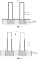
- FIG. 1 to FIG. 11 are schematic structural diagrams corresponding to various steps of a manufacturing method of a semiconductor structure according to an embodiment of the present disclosure.
- a method for reducing the parasitic capacitance may include: forming a sacrificial layer between a conducting layer and an insulating layer which are adjacent, removing the sacrificial layer to form a gap, and sealing the gap. Since there is air in the gap and a dielectric constant of the air is low, the parasitic capacitance can be reduced. In a process step of sealing the gap, part of reaction gas can enter the gap and form a deposition layer at a bottom of the gap, thereby reducing the size of the gap.
- the above method has a poor effect of reducing parasitic capacitance, and may also affect the yield of the semiconductor structure.
- the manufacturing method of a semiconductor structure includes: providing a base with an electrical contact layer therein; forming an insulating layer on the base, the insulating layer having a through hole penetrating the insulating layer, and the through hole exposing a surface of the electrical contact layer; forming a sidewall layer on a sidewall of the through hole; forming a first isolation layer, the first isolation layer covering a surface of the sidewall layer and an exposed surface of the insulating layer; removing the sidewall layer to form a gap between the first isolation layer and the insulating layer; and forming a conducting layer filling the through hole, the conducting layer being electrically connected to the electrical contact layer.
- the first isolation layer covers the entire surface of the sidewall layer, the gap formed after the removal of the sidewall layer is completely surrounded by the first isolation layer and does not need to be sealed, thereby ensuring that the parasitic capacitance can be reduced to a great extent and improving the yield of the semiconductor structure.
- FIG. 1 to FIG. 11 are schematic structural diagrams corresponding to various steps of a manufacturing method of a semiconductor structure according to a first embodiment of the present disclosure. A detailed description will be given below in conjunction with the drawings.
- a base 100 with an electrical contact layer 101 therein is provided.
- the base 100 may include structures such as wordlines, bitlines, sources, drains and the like.
- the base 100 may be made of silicon, sapphire, silicon carbide, gallium arsenide, aluminum nitride, zinc silicon oxide, or the like.
- the electrical contact layer 101 is configured to achieve electrical connection between an internal structure of the base 100 and a conducting layer formed subsequently.
- the subsequently-formed conducting layer may be electrically connected to the bitlines in the base 100 through the electrical contact layer.
- the electrical contact layer 101 is made of copper.
- the electrical contact layer 101 may also be made of a conducting material, such as polysilicon, tungsten, titanium, or the like.
- the base 100 further has isolation structures 102 therein, and the isolation structure 102 is configured to isolate adjacent electrical contact layers 101.
- the isolation structure 102 is made of silicon oxide.
- the isolation structure 102 may also be made of an insulating material such as silicon carbide, silicon nitride, or the like.
- an insulating layer 103 is formed on the base 100.
- the insulating layer 103 has a through hole 110 penetrating the insulating layer 103, and the through hole 110 exposes a surface of the electrical contact layer 101.
- the insulating layer 103 is configured to isolate the conducting layer formed in the through hole 110 subsequently.
- the insulating layer 103 is located on the isolation structure 102, and in a direction parallel to a surface of the base 100, the isolation structure 102 is wider than the insulating layer 103 for the following reason: a gap, a first isolation layer and a second isolation layer will be formed subsequently on a sidewall of the insulating layer 103, the isolation structure 102 is wider than the insulating layer 103, and when a width difference meets a certain value range, the gap, the first isolation layer and the second isolation layer can directly face the isolation structure 102, so that the entire surface of the electrical contact layer 101 is exposed to increase a contact area between the subsequently-formed conducting layer and the electrical contact layer 101, thereby reducing contact resistance.
- a width of the insulating layer 103 is greater than or equal to one-half of a width of the isolation structure 102 and less than or equal to the width of the isolation structure 102.
- the width of the insulating layer 103 is within the above range, the first and second isolation layers to be formed subsequently can be well supported and the stability of the semiconductor structure can be improved; and moreover enough space can also be reserved for the gap, the first isolation layer and the second isolation layer to be formed subsequently, so that the gap, the first isolation layer and the second isolation layer can be located on the isolation structure 102, and the entire surface of the electrical contact layer 101 can be exposed to increase the contact area between the subsequently-formed conducting layer and the electrical contact layer 101.
- the insulating layer 103 and the isolation structure 102 are made of a same material, which can improve the tightness of adhesion between the insulating layer 103 and the isolation structure 102, thereby improving the stability of the semiconductor structure.
- the insulating layer 103 and the isolation structure 102 are both made of silicon dioxide.
- the insulating layer 103 may also be made of a different material from the isolation layer; for example, the insulating layer 103 may be made of an insulating material such as silicon carbide, silicon nitride, or the like.
- the process step for forming the insulating layer 103 and the through hole 110 is as follows. Referring to FIG. 1 , an initial insulating layer 103a is formed on the base 100, and a patterned photoresist layer 104 is formed on the initial insulating layer 103a; referring to FIG. 2 , using the patterned photoresist layer 104 (see FIG. 1 ) as a mask, the initial insulating layer 103a (see FIG. 1 ) is etched to form the insulating layer 103.
- a chemical vapor deposition process is carried out to form the initial insulating layer 103a.
- the chemical vapor deposition process has a high deposition rate and can shorten a process time.
- a dry etching method is carried out to etch the initial insulating layer 103a until the electrical contact layer 101 is exposed, thus forming the insulating layer 103 and the through hole 110 exposing the electrical contact layer 101.
- a sidewall layer 105 is formed on the sidewall of the through hole 110.
- the sidewall layer 105 is configured to occupy a spatial position for the subsequent formation of the gap; that is, the position of the sidewall layer 105 is the position of the subsequently-formed gap.
- the sidewall layer 105 should be made of a material which can be decomposed easily. In this way, during the subsequent removal of the sidewall layer 105 to form the gap, under the action of oxygen plasma, the sidewall layer 105 can be discharged as a gas after being decomposed.
- the sidewall layer 105 is made of amorphous carbon, hydrocarbon or a polymer, for example, C x H y .
- a ratio of a height of the sidewall layer 105 to a height of the insulating layer 103 is greater than or equal to 0.3. That is, a top surface of the sidewall layer 105 may be flush with a top surface of the insulating layer 103 or may be lower than the top surface of the insulating layer 103.
- the ratio of the height of the sidewall layer 105 to the height of the insulating layer 103 is greater than or equal to 0.3, the greater the height of the sidewall layer 105, the greater the height of the gap to be formed subsequently, so that the parasitic capacitance can be reduced to a great extent.
- the top surface of the sidewall layer 105 is lower than the top surface of the insulating layer 103, and the ratio of the height of the sidewall layer 105 to the height of the insulating layer 103 is less than or equal to 0.8.
- the subsequently-formed first isolation layer can be located on the sidewall of the insulating layer 103 exposed by the sidewall layer 105; that is, the subsequently-formed first isolation layer can be well supported by the sidewall of the insulating layer 103, so that the first isolation layer is not likely to collapse and has a good stability.
- the step of forming the sidewall layer 105 will be described in detail below.
- an initial sidewall layer 105a is formed on a surface of the insulating layer 103 and a bottom of the through hole 110.
- an atomic layer deposition process is carried out to form the initial sidewall layer 105a.
- the initial sidewall layer 105a formed by the atomic layer deposition process has a relatively even thickness.
- a chemical vapor deposition process or a physical vapor deposition process may also be carried out to form the initial sidewall layer 105a.
- the initial sidewall layer 105a located at the bottom of the through hole 110 and the top surface of the insulating layer 103 is removed (see FIG. 3 ), and part of the initial sidewall layer 105a located on the sidewall of the through hole 110 is also removed; the remaining initial sidewall layer 105a serves as the sidewall layer 105a.
- the top surface of the sidewall layer 105 is lower than the top surface of the insulating layer 103, so that the first isolation layer formed subsequently also covers the sidewall of the insulating layer 103 exposed by the sidewall layer 105. In this way, after the sidewall layer 105 is removed, since the first isolation layer is still supported by the sidewall of the insulating layer 103, the first isolation layer has the good stability.
- the initial sidewall layer 105a located on the sidewall of the through hole 110 may not be removed; that is, the top surface of the formed sidewall layer 105 is flush with the top surface of the insulating layer 103, and the first isolation layer formed subsequently can not cover the sidewall of the insulating layer 103.
- part of the initial insulating layer 105a is removed by dry etching (see FIG. 3 ).
- a first isolation layer 106 is formed, and the first isolation layer 106 covers the surface of the sidewall layer 105 and an exposed surface of the insulating layer 103.
- the first isolation layer 106 is required to be decomposed hardly. Therefore, the first isolation layer 106 is unlikely to be damaged during the subsequent removal of the sidewall layer 105 and thus achieves a better stability.
- the first isolation layer 106 is relatively thin; for example, the thickness thereof may be less than 3 nm, so that an ion beam can more easily pass through the first isolation layer 106 and remove the sidewall layer 105.
- the first isolation layer 106 has holes, so that the ion beam can directly pass through the holes, and therefore the sidewall layer 105 can be removed more thoroughly.
- the first isolation layer 106 is made of silicon dioxide. In other embodiments, the first isolation layer 106 may also be made of a silicon-oxyhydrocarbon. The silicon dioxide or silicon-oxyhydrocarbon is hardly decomposed under the action of oxygen plasma and has the good stability.
- the first isolation layer 106 is formed by a low-temperature atomic layer deposition process. In this way, a thin first isolation layer 106 can be formed, so that the sidewall layer 105 completely covered by the first isolation layer 106 can be more easily removed later.
- a temperature range of the low-temperature atomic layer deposition process is in a low-temperature range of 50 °C to 135 °C. Through the low-temperature atomic layer deposition process, the thickness of the first isolation layer 106 can be more accurately controlled to obtain a homogeneous thin first isolation layer 106, and the first isolation layer 106 can have the characteristics of a flatter surface.
- the sidewall layer 105 is removed (see FIG. 5 ) to form a gap 107 between the first isolation layer 106 and the insulating layer 103.
- a method for removing the sidewall layer 105 includes: providing a plasma source, causing an ion beam generated by the plasma source to react with the sidewall layer 105 after passing through the first isolation layer 106 and form reaction byproducts, and discharging at least part of the reaction byproducts through the first isolation layer 106.
- the above method has the advantages of fewer residues and higher cleanliness when used for removing the sidewall layer 105.
- oxygen is used as the plasma source
- the process steps for removing the sidewall layer 105 include: generating an ion beam based on the oxygen plasma source, and causing the ion beam to pass through the first isolation layer 106 through the holes in the first isolation layer 106 and react with the sidewall layer 105 (see FIG. 5 ), so that the sidewall layer 105 is thermally decomposed to produce reaction byproducts such as carbon dioxide, carbon monoxide, water, methane and the like. Gases such as carbon dioxide, carbon monoxide, water and methane can pass through the holes in the first isolation layer 106 to be discharged.
- a flow rate of oxygen is within a range of 100 sccm to 600 sccm.
- oxygen can react sufficiently with the material of the sidewall layer 105, so that the sidewall layer 105 can be more completely removed; and the first isolation layer 106 can be prevented from major damage, thus ensuring that the first isolation layer 106 has a high stability.
- a radio frequency power is within a range of 500W to 1000W.
- the ion beam has sufficient energy to completely remove the sidewall layer 105; and major damage to the first isolation layer 106 can also be prevented, ensuring that the first isolation layer 106 has a high stability.
- a second isolation layer 108 is formed on the surface of the first isolation layer 106.
- a density of the second isolation layer 108 is greater than that of the first isolation layer 106.
- the first isolation layer 106 in order to make more ion beams pass through the first isolation layer 106, so that the sidewall layer 105 is removed more completely, and the first isolation layer 106 has a lower density; after the removal of the sidewall layer 105, formation of the denser second isolation layer 108 on the surface of the first isolation layer 106 can increase the density of the first isolation layer 106, thereby improving the firmness and stability of the first isolation layer 106.
- the thickness of the second isolation layer 108 is greater than the thickness of the first isolation layer 106, which can further improve the firmness of the first isolation layer 106.
- a ratio of the thickness of the second isolation layer 108 to the thickness of the first isolation layer 106 is within a range of 1.5:1 to 3:1.
- the second isolation layer 108 can well reinforce the first isolation layer 106.
- the second isolation layer 108 can occupy a reasonable area on the isolation structure 102, so that the second isolation layer 108 can completely expose the surface of the electrical contact layer 101, so as to increase the contact area between the electrical contact layer 101 and the subsequently-formed conducting layer.
- the second isolation layer 108 and the first isolation layer 106 are made of a same material, which can ensure that the second isolation layer 108 and the first isolation layer 106 can be more closely attached, thereby further improving the reinforcement effect of the second isolation layer 108.
- the second isolation layer 108 and the first isolation layer 106 are both made of silicon dioxide.
- the second isolation layer 108 may also be made of a different material from the first isolation layer 106; for example, the second isolation layer 108 may be made of silicon nitride.
- the second isolation layer 108 is formed by an atomic layer deposition process or a chemical vapor deposition process with better step coverage.
- the first isolation layer 106 and the second isolation layer 108 located at the bottom of the through hole 110 and the top surface of the insulating layer 103 are removed.
- a dry etching method is carried out to remove part of the first isolation layer 106 and part of the second isolation layer 108.
- the remaining first isolation layer 106 and the remaining second isolation layer 108 expose the entire surface of the electrical contact layer 101, thereby increasing the contact area between the subsequently-formed conducting layer and the electrical contact layer 101 and reducing the contact resistance.
- the remaining first isolation layer 106 and the remaining second isolation layer 108 may also expose only part of the surface of the electrical contact layer 101.
- a barrier layer 109 covering the sidewall of the through hole 110 is deposited.
- the barrier layer 109 is configured to block mutual diffusion between atoms in the subsequently-formed conducting layer and atoms in the second isolation layer 108, and meanwhile can also increase the adhesion between the conducting layer and the second isolation layer 108, thereby improving the stability and firmness of the subsequently-formed conducting layer.
- the barrier layer 109 is also located at the bottom of the through hole 110.
- the barrier layer 109 can also block the mutual diffusion between the atoms in the subsequently-formed conducting layer and atoms in the electrical contact layer 101, and meanwhile can also increase the adhesion between the conducting layer and the electrical contact layer 101.
- the barrier layer 109 is made of tantalum, tantalum nitride, ruthenium, or rhenium.
- the barrier layer 109 is formed by an atomic layer deposition process.
- a conducting layer 111 filling the through hole 110 (see FIG. 9 ) is formed, and the conducting layer 111 is electrically connected to the electrical contact layer 101.
- the conducting layer 111 is also higher than the top of the insulating layer 103.
- the conducting layer 111 connects the structures in the base 100 together according to design requirements to achieve specific functions.
- the conducting layer 111 is made of copper, gold, silver, titanium or tungsten.
- the conducting layer 111 is formed by a chemical vapor deposition process. In other embodiments, a physical vapor deposition process may also be carried out to form the conducting layer 111.
- planarization is performed to remove part of the conducting layer 111, part of the insulating layer 103, part of the first isolation layer 106 and part of the second isolation layer 108 which are higher than the gap 107.
- the process should be stopped at a position higher than the gap 107, so as to ensure that the gap 107 is still in a sealed state.
- the planarization is performed by chemical mechanical polishing.
- the gap formed is located on the entire sidewall of the insulating layer 103; that is, in a direction perpendicular to the surface of the base 100, the gap is as high as the insulating layer 103; then, during the planarization, in order to ensure the tightness of the gap, only the conducting layer 111 higher than the gap may be removed, while the insulating layer 103, the first isolation layer 106, the second isolation layer 108, and the barrier layer 109 are retained.
- the sidewall layer covered by the first isolation layer is removed by a plasma process, thereby forming a gap.
- a process step of sealing the gap is not required, so that the gap has a larger size and high stability, which can effectively reduce the parasitic capacitance of the semiconductor structure.
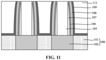
- FIG. 11 is a schematic diagram of the semiconductor structure according to the second embodiment of the present disclosure.
- the semiconductor structure includes: a base 100 with an electrical contact layer 101 therein; an insulating layer 103 located on the base 100, the insulating layer 103 having a conducting layer 111 therein, and the conducting layer 111 being electrically connected to the electrical contact layer 101; and a first isolation layer 106, the first isolation layer being located between the insulating layer 103 and the conducting layer 111, the first isolation layer 106 being also located on part of sidewalls of the insulating layer 103, a gap 107 existing between the insulating layer 103 and the first isolation layer 106, and the gap 107 being sealed by the first isolation layer 106.
- the base 100 may include structures such as wordlines, bitlines, sources, drains and the like.
- the base 100 may be made of silicon, sapphire, silicon carbide, gallium arsenide, aluminum nitride, zinc silicon oxide, or the like.
- the electrical contact layer 101 is configured to achieve electrical connection between an internal structure of the base 100 and the conducting layer 111.
- the conducting layer 111 may be electrically connected to the bitlines in the base 100 through the electrical contact layer 101.
- the electrical contact layer 101 is made of copper.
- the electrical contact layer 101 may also be made of a conducting material, such as polysilicon, tungsten, titanium, or the like.
- the base 100 further has isolation structures 102 therein, and the isolation structure 102 is configured to isolate adjacent electrical contact layers 101.
- the isolation structure 102 is made of silicon oxide.
- the isolation structure 102 may also be made of an insulating material such as silicon carbide, silicon nitride, or the like.
- the insulating layer 103 is configured to isolate adjacent conducting layers 111.
- the insulating layer 103 is located on the isolation structure 102, and in a direction parallel to a surface of the base 100, the isolation structure 102 is wider than the insulating layer 103 for the following reason: a gap, a first isolation layer and a second isolation layer will be formed subsequently on a sidewall of the insulating layer 103, the isolation structure 102 is wider than the insulating layer 103, and when a width difference meets a certain value range, the gap, the first isolation layer and the second isolation layer can directly face the isolation structure 102, so that the entire surface of the electrical contact layer 101 is exposed to increase a contact area between the subsequently-formed conducting layer and the electrical contact layer 101, thereby reducing contact resistance.
- a width of the insulating layer 103 is greater than or equal to one-half of a width of the isolation structure 102 and less than or equal to the width of the isolation structure 102.
- the width of the insulating layer 103 is within the above range, the first isolation layer 106 and the second isolation layer 108 can be well supported and the stability of the semiconductor structure can be improved; and moreover enough space can also be reserved for the gap 107, the first isolation layer 106 and the second isolation layer 108, so that the gap 107, the first isolation layer 106 and the second isolation layer 108 can be located on the isolation structure 102, and the entire surface of the electrical contact layer 101 can be exposed to increase the contact area between the conducting layer 111 and the electrical contact layer 101.
- the insulating layer 103 is made of silicon dioxide, silicon nitride, or silicon carbide.
- the conducting layer 111 connects the structures in the base 100 together according to design requirements to achieve specific functions.
- the conducting layer 111 is made of copper, gold, silver, titanium, or tin.
- the first isolation layer 106 is configured to seal the gap 107. Since the first isolation layer 106 is also located on the top of the gap 107, the gap 107 does not need other isolation layers for sealing.
- the first isolation layer 106 is also located on the isolation structure 102 and exposes the entire surface of the electrical contact layer 101 to increase the contact area between the electrical contact layer 101 and the conducting layer 111 and reduce the contact resistance.
- the second isolation layer 108 covers the surface of the first isolation layer 106, and a density of the second isolation layer 108 is greater than that of the first isolation layer 106.
- the denser second isolation layer 108 can increase the density of the first isolation layer 106, thereby improving the firmness and stability of the first isolation layer 106.
- the thickness of the second isolation layer 108 is greater than the thickness of the first isolation layer 106. In this way, the stability of the first isolation layer 106 can be improved, and problems such as collapse of the first isolation layer 106 can be avoided.
- a ratio of the thickness of second isolation layer 108 to the thickness of the first isolation layer 106 is within a range of 1.5:1 to 3:1.
- the second isolation layer 108 can well reinforce the first isolation layer 106.
- the second isolation layer 108 can occupy a reasonable area on the isolation structure 102, so that the second isolation layer 108 can completely expose the surface of the electrical contact layer 101, so as to increase the contact area between the electrical contact layer 101 and the conducting layer 111.
- the first isolation layer 106 and the second isolation layer 108 are both located on the base 100 other than the electrical contact layer 101 and expose the entire surface of the electrical contact layer 101. In this way, the contact area between the conducting layer 111 and the electrical contact layer 101 can be increased, thereby reducing the contact resistance and increasing the operating speed of the semiconductor structure.
- the first isolation layer 106 is made of silicon dioxide. In other embodiments, the first isolation layer 106 may also be made of a silicon-oxyhydrocarbon. The silicon dioxide or silicon-oxyhydrocarbon is hardly decomposed under the action of oxygen plasma and has good stability.
- the second isolation layer 108 and the first isolation layer 106 are made of a same material, which can ensure that the second isolation layer 108 and the first isolation layer 106 can be more closely attached, thereby further improving the reinforcement effect of the second isolation layer 108.
- the second isolation layer 108 and the first isolation layer 106 are both made of silicon dioxide.
- the second isolation layer 108 may also be made of a different material from the first isolation layer 106; for example, the second isolation layer 108 may be made of silicon nitride.
- a width of the gap 107 may be within a range of 1 nm to 5 nm.
- the width of the gap 107 is within the above range, the parasitic capacitance can be effectively reduced, and the stability of the first isolation layer 106 and the second isolation layer 108 can be ensured.
- a ratio of a height of the gap 107 to a height of the insulating layer 103 is greater than or equal to 0.3.
- the height of the gap 107 is within the above range; that is, the gap 107 occupies a large space and can reduce the parasitic capacitance to a great extent.
- the ratio of the height of the gap 107 to the height of the insulating layer 103 is greater than or equal to 0.9. That is, the contact area between the first isolation layer 106 and the insulating layer 103 is greater than or equal to 0.1 of a total area of the sidewall of the insulating layer 103. If the contact area is within the above range, the first isolation layer 106 can be more closely attached to the sidewall of the insulating layer 103, thereby ensuring that the first isolation layer 106 can completely seal the top of the gap 107, so that the gap 107 has good airtightness and stability. In this way, the parasitic capacitance can be reduced effectively.
- the semiconductor structure further includes a barrier layer 109 located between the first isolation layer 106 and the conducting layer 111.
- the barrier layer 109 covers the surface of the second isolation layer 108.
- the barrier layer 109 is configured to block mutual diffusion between atoms of the conducting layer 111 and atoms in the second isolation layer 108 and increase the adhesion between the barrier layer 109 and the second isolation layer 108.
- the barrier layer 109 also covers the surface of the electrical contact layer 101.
- the barrier layer 109 is also configured to block the mutual diffusion between the atoms in the conducting layer 111 and atoms in the electrical contact layer 101 and increase the adhesion between the barrier layer 109 and the electrical contact layer 101.
- the barrier layer 109 is made of tantalum, tantalum nitride, ruthenium, or rhenium.
- the first isolation layer 106 completely seals the gap 107, so that the gap 107 has good airtightness and stability, which can effectively reduce the parasitic capacitance.
Landscapes
- Internal Circuitry In Semiconductor Integrated Circuit Devices (AREA)
Abstract
Description
- This application is based on
Chinese Patent Application No. 202110003495.3, filed on January 4, 2021 - Embodiments of the present disclosure relate to the field of semiconductors, and in particular to a manufacturing method of a semiconductor structure and a semiconductor structure.
- With the development of semiconductor manufacturing technologies, the critical dimension of the semiconductor process has shrunk to the order of deep submicron. Due to the continuous shrinking of the critical dimension, a distance between interconnection lines in a semiconductor structure is getting closer, and parasitic capacitance is getting larger and larger. The parasitic capacitance can seriously affect the performance of the semiconductor structure, and especially reduce the operating speed and reliability of the semiconductor structure.
- Therefore, how to reduce the parasitic capacitance in the semiconductor structure is currently an urgent technical problem to be solved.
- The embodiments of the present disclosure provide a manufacturing method of a semiconductor structure and a semiconductor structure to reduce parasitic capacitance in the semiconductor structure.
- In order to solve the above problem, an embodiment of the present disclosure provides a manufacturing method of a semiconductor structure, including: providing a base with an electrical contact layer therein; forming an insulating layer on the base, the insulating layer having a through hole penetrating the insulating layer, and the through hole exposing a surface of the electrical contact layer; forming a sidewall layer on a sidewall of the through hole; forming a first isolation layer, the first isolation layer covering a surface of the sidewall layer and an exposed surface of the insulating layer; removing the sidewall layer to form a gap between the first isolation layer and the insulating layer; and forming a conducting layer filling the through hole, the conducting layer being electrically connected to the electrical contact layer.
- An embodiment of the present disclosure further provides a semiconductor structure, including: a base with an electrical contact layer therein; an insulating layer located on the base, the insulating layer having a conducting layer therein, and the conducting layer being electrically connected to the electrical contact layer; and a first isolation layer located between the insulating layer and the conducting layer, the first isolation layer being also located on part of the sidewall of the insulating layer, a gap existing between the insulating layer and the first isolation layer, and the first isolation layer sealing the gap.
- Compared with a prior art, the technical solution according to the embodiments of the present disclosure has the following advantages.
- In the manufacturing method of a semiconductor structure according to the embodiment of the present disclosure, the first isolation layer covering the surface of the sidewall layer is formed, that is, also covers a top of the sidewall layer; after the sidewall layer is removed to form the gap, the first isolation layer completely seals the gap, and a step of sealing the gap is no longer required, thereby avoiding the formation of a deposition layer in the gap during the sealing process, or situations such as improper sealing, and then effectively reducing the parasitic capacitance of the semiconductor structure.
- In addition, the method for removing the sidewall layer includes: providing a plasma source, causing an ion beam generated by the plasma source to react with the sidewall layer after passing through the first isolation layer and form reaction byproducts, and discharging at least part of the reaction byproducts through the first isolation layer. Compared with a wet process, in this method, fewer residues are generated, and the sidewall layer can be removed more thoroughly.
- One or more embodiments are exemplified by pictures in the corresponding drawings. These exemplified descriptions do not constitute a limitation on the embodiments. Elements with the same reference numerals in the drawings are denoted as similar elements. Unless otherwise stated, the figures in the accompanying drawings do not constitute a scale limitation.
-
FIG. 1 to FIG. 11 are schematic structural diagrams corresponding to various steps of a manufacturing method of a semiconductor structure according to an embodiment of the present disclosure. - It can be seen from the Background section that the parasitic capacitance in a semiconductor structure needs to be further reduced. A method for reducing the parasitic capacitance may include: forming a sacrificial layer between a conducting layer and an insulating layer which are adjacent, removing the sacrificial layer to form a gap, and sealing the gap. Since there is air in the gap and a dielectric constant of the air is low, the parasitic capacitance can be reduced. In a process step of sealing the gap, part of reaction gas can enter the gap and form a deposition layer at a bottom of the gap, thereby reducing the size of the gap. In addition, if improper sealing occurs, during subsequent deposition of a conducting material, the conducting material is likely to enter the gap, thereby causing electrical conduction between interconnection lines that should be isolated from each other. Therefore, the above method has a poor effect of reducing parasitic capacitance, and may also affect the yield of the semiconductor structure.
- In order to solve the above problem, embodiments of the present disclosure provide a manufacturing method of a semiconductor structure and a semiconductor structure. The manufacturing method of a semiconductor structure includes: providing a base with an electrical contact layer therein; forming an insulating layer on the base, the insulating layer having a through hole penetrating the insulating layer, and the through hole exposing a surface of the electrical contact layer; forming a sidewall layer on a sidewall of the through hole; forming a first isolation layer, the first isolation layer covering a surface of the sidewall layer and an exposed surface of the insulating layer; removing the sidewall layer to form a gap between the first isolation layer and the insulating layer; and forming a conducting layer filling the through hole, the conducting layer being electrically connected to the electrical contact layer. Since the first isolation layer covers the entire surface of the sidewall layer, the gap formed after the removal of the sidewall layer is completely surrounded by the first isolation layer and does not need to be sealed, thereby ensuring that the parasitic capacitance can be reduced to a great extent and improving the yield of the semiconductor structure.
- In order to make the objectives, technical solutions, and advantages of the embodiments of the present disclosure more clear, various embodiments of the present disclosure will be detailed below in combination with the accompanying drawings. However, a person of ordinary skill in the art can understand that in each embodiment of the present disclosure, many technical details are provided for readers to better understand the present disclosure. However, even if these technical details are not provided and based on variations and modifications of the following embodiments, the technical solutions sought for protection in the present disclosure can also be implemented.
-
FIG. 1 to FIG. 11 are schematic structural diagrams corresponding to various steps of a manufacturing method of a semiconductor structure according to a first embodiment of the present disclosure. A detailed description will be given below in conjunction with the drawings. - Referring to
FIG. 1 , abase 100 with anelectrical contact layer 101 therein is provided. Thebase 100 may include structures such as wordlines, bitlines, sources, drains and the like. Thebase 100 may be made of silicon, sapphire, silicon carbide, gallium arsenide, aluminum nitride, zinc silicon oxide, or the like. - The
electrical contact layer 101 is configured to achieve electrical connection between an internal structure of thebase 100 and a conducting layer formed subsequently. In an example, the subsequently-formed conducting layer may be electrically connected to the bitlines in thebase 100 through the electrical contact layer. In the present embodiment, theelectrical contact layer 101 is made of copper. In other embodiments, theelectrical contact layer 101 may also be made of a conducting material, such as polysilicon, tungsten, titanium, or the like. - In the present embodiment, the
base 100 further hasisolation structures 102 therein, and theisolation structure 102 is configured to isolate adjacentelectrical contact layers 101. In the present embodiment, theisolation structure 102 is made of silicon oxide. In other embodiments, theisolation structure 102 may also be made of an insulating material such as silicon carbide, silicon nitride, or the like. - Referring to
FIG. 1 to FIG. 2 , aninsulating layer 103 is formed on thebase 100. Theinsulating layer 103 has a throughhole 110 penetrating theinsulating layer 103, and the throughhole 110 exposes a surface of theelectrical contact layer 101. - The
insulating layer 103 is configured to isolate the conducting layer formed in the throughhole 110 subsequently. - The
insulating layer 103 is located on theisolation structure 102, and in a direction parallel to a surface of thebase 100, theisolation structure 102 is wider than theinsulating layer 103 for the following reason: a gap, a first isolation layer and a second isolation layer will be formed subsequently on a sidewall of theinsulating layer 103, theisolation structure 102 is wider than theinsulating layer 103, and when a width difference meets a certain value range, the gap, the first isolation layer and the second isolation layer can directly face theisolation structure 102, so that the entire surface of theelectrical contact layer 101 is exposed to increase a contact area between the subsequently-formed conducting layer and theelectrical contact layer 101, thereby reducing contact resistance. - A width of the
insulating layer 103 is greater than or equal to one-half of a width of theisolation structure 102 and less than or equal to the width of theisolation structure 102. When the width of theinsulating layer 103 is within the above range, the first and second isolation layers to be formed subsequently can be well supported and the stability of the semiconductor structure can be improved; and moreover enough space can also be reserved for the gap, the first isolation layer and the second isolation layer to be formed subsequently, so that the gap, the first isolation layer and the second isolation layer can be located on theisolation structure 102, and the entire surface of theelectrical contact layer 101 can be exposed to increase the contact area between the subsequently-formed conducting layer and theelectrical contact layer 101. - In the present embodiment, the
insulating layer 103 and theisolation structure 102 are made of a same material, which can improve the tightness of adhesion between theinsulating layer 103 and theisolation structure 102, thereby improving the stability of the semiconductor structure. For example, theinsulating layer 103 and theisolation structure 102 are both made of silicon dioxide. In other embodiments, theinsulating layer 103 may also be made of a different material from the isolation layer; for example, theinsulating layer 103 may be made of an insulating material such as silicon carbide, silicon nitride, or the like. - Specifically, the process step for forming the
insulating layer 103 and the throughhole 110 is as follows. Referring toFIG. 1 , aninitial insulating layer 103a is formed on thebase 100, and a patternedphotoresist layer 104 is formed on theinitial insulating layer 103a; referring toFIG. 2 , using the patterned photoresist layer 104 (seeFIG. 1 ) as a mask, theinitial insulating layer 103a (seeFIG. 1 ) is etched to form theinsulating layer 103. - In the present embodiment, a chemical vapor deposition process is carried out to form the initial
insulating layer 103a. The chemical vapor deposition process has a high deposition rate and can shorten a process time. - In the present embodiment, a dry etching method is carried out to etch the
initial insulating layer 103a until theelectrical contact layer 101 is exposed, thus forming theinsulating layer 103 and the throughhole 110 exposing theelectrical contact layer 101. - Referring to
FIG. 3 to FIG. 4 , asidewall layer 105 is formed on the sidewall of thethrough hole 110. - The
sidewall layer 105 is configured to occupy a spatial position for the subsequent formation of the gap; that is, the position of thesidewall layer 105 is the position of the subsequently-formed gap. - The
sidewall layer 105 should be made of a material which can be decomposed easily. In this way, during the subsequent removal of thesidewall layer 105 to form the gap, under the action of oxygen plasma, thesidewall layer 105 can be discharged as a gas after being decomposed. Thesidewall layer 105 is made of amorphous carbon, hydrocarbon or a polymer, for example, CxHy. - In the present embodiment, in a direction perpendicular to the surface of the
base 100, a ratio of a height of thesidewall layer 105 to a height of the insulatinglayer 103 is greater than or equal to 0.3. That is, a top surface of thesidewall layer 105 may be flush with a top surface of the insulatinglayer 103 or may be lower than the top surface of the insulatinglayer 103. - When the ratio of the height of the
sidewall layer 105 to the height of the insulatinglayer 103 is greater than or equal to 0.3, the greater the height of thesidewall layer 105, the greater the height of the gap to be formed subsequently, so that the parasitic capacitance can be reduced to a great extent. - Preferably, the top surface of the
sidewall layer 105 is lower than the top surface of the insulatinglayer 103, and the ratio of the height of thesidewall layer 105 to the height of the insulatinglayer 103 is less than or equal to 0.8. In this way, the subsequently-formed first isolation layer can be located on the sidewall of the insulatinglayer 103 exposed by thesidewall layer 105; that is, the subsequently-formed first isolation layer can be well supported by the sidewall of the insulatinglayer 103, so that the first isolation layer is not likely to collapse and has a good stability. - The step of forming the
sidewall layer 105 will be described in detail below. - Referring to
FIG. 3 , aninitial sidewall layer 105a is formed on a surface of the insulatinglayer 103 and a bottom of the throughhole 110. In the present embodiment, an atomic layer deposition process is carried out to form theinitial sidewall layer 105a. Theinitial sidewall layer 105a formed by the atomic layer deposition process has a relatively even thickness. In other embodiments, a chemical vapor deposition process or a physical vapor deposition process may also be carried out to form theinitial sidewall layer 105a. - Referring to
FIG. 4 , theinitial sidewall layer 105a located at the bottom of the throughhole 110 and the top surface of the insulatinglayer 103 is removed (seeFIG. 3 ), and part of theinitial sidewall layer 105a located on the sidewall of the throughhole 110 is also removed; the remaininginitial sidewall layer 105a serves as thesidewall layer 105a. - That is, the top surface of the
sidewall layer 105 is lower than the top surface of the insulatinglayer 103, so that the first isolation layer formed subsequently also covers the sidewall of the insulatinglayer 103 exposed by thesidewall layer 105. In this way, after thesidewall layer 105 is removed, since the first isolation layer is still supported by the sidewall of the insulatinglayer 103, the first isolation layer has the good stability. - In other embodiments, the
initial sidewall layer 105a located on the sidewall of the throughhole 110 may not be removed; that is, the top surface of the formedsidewall layer 105 is flush with the top surface of the insulatinglayer 103, and the first isolation layer formed subsequently can not cover the sidewall of the insulatinglayer 103. - In the present embodiment, part of the initial insulating
layer 105a is removed by dry etching (seeFIG. 3 ). - Referring to
FIG. 5 , afirst isolation layer 106 is formed, and thefirst isolation layer 106 covers the surface of thesidewall layer 105 and an exposed surface of the insulatinglayer 103. - Compared with the
sidewall layer 105, thefirst isolation layer 106 is required to be decomposed hardly. Therefore, thefirst isolation layer 106 is unlikely to be damaged during the subsequent removal of thesidewall layer 105 and thus achieves a better stability. - In addition, the
first isolation layer 106 is relatively thin; for example, the thickness thereof may be less than 3 nm, so that an ion beam can more easily pass through thefirst isolation layer 106 and remove thesidewall layer 105. - In addition, the
first isolation layer 106 has holes, so that the ion beam can directly pass through the holes, and therefore thesidewall layer 105 can be removed more thoroughly. - In the present embodiment, the
first isolation layer 106 is made of silicon dioxide. In other embodiments, thefirst isolation layer 106 may also be made of a silicon-oxyhydrocarbon. The silicon dioxide or silicon-oxyhydrocarbon is hardly decomposed under the action of oxygen plasma and has the good stability. - In the present embodiment, the
first isolation layer 106 is formed by a low-temperature atomic layer deposition process. In this way, a thinfirst isolation layer 106 can be formed, so that thesidewall layer 105 completely covered by thefirst isolation layer 106 can be more easily removed later. A temperature range of the low-temperature atomic layer deposition process is in a low-temperature range of 50 °C to 135 °C. Through the low-temperature atomic layer deposition process, the thickness of thefirst isolation layer 106 can be more accurately controlled to obtain a homogeneous thinfirst isolation layer 106, and thefirst isolation layer 106 can have the characteristics of a flatter surface. - Referring to
FIG. 6 , thesidewall layer 105 is removed (seeFIG. 5 ) to form agap 107 between thefirst isolation layer 106 and the insulatinglayer 103. - A method for removing the sidewall layer 105 (see
FIG. 5 ) includes: providing a plasma source, causing an ion beam generated by the plasma source to react with thesidewall layer 105 after passing through thefirst isolation layer 106 and form reaction byproducts, and discharging at least part of the reaction byproducts through thefirst isolation layer 106. Compared with a wet process, the above method has the advantages of fewer residues and higher cleanliness when used for removing thesidewall layer 105. - In the present embodiment, oxygen is used as the plasma source, and the process steps for removing the
sidewall layer 105 include: generating an ion beam based on the oxygen plasma source, and causing the ion beam to pass through thefirst isolation layer 106 through the holes in thefirst isolation layer 106 and react with the sidewall layer 105 (seeFIG. 5 ), so that thesidewall layer 105 is thermally decomposed to produce reaction byproducts such as carbon dioxide, carbon monoxide, water, methane and the like. Gases such as carbon dioxide, carbon monoxide, water and methane can pass through the holes in thefirst isolation layer 106 to be discharged. - A flow rate of oxygen is within a range of 100 sccm to 600 sccm. When the flow rate of oxygen is within the above range, oxygen can react sufficiently with the material of the
sidewall layer 105, so that thesidewall layer 105 can be more completely removed; and thefirst isolation layer 106 can be prevented from major damage, thus ensuring that thefirst isolation layer 106 has a high stability. - A radio frequency power is within a range of 500W to 1000W. When the radio frequency power is within the above range, the ion beam has sufficient energy to completely remove the
sidewall layer 105; and major damage to thefirst isolation layer 106 can also be prevented, ensuring that thefirst isolation layer 106 has a high stability. - Referring to
FIG. 7 , asecond isolation layer 108 is formed on the surface of thefirst isolation layer 106. A density of thesecond isolation layer 108 is greater than that of thefirst isolation layer 106. - It can be understood that, in order to make more ion beams pass through the
first isolation layer 106, so that thesidewall layer 105 is removed more completely, and thefirst isolation layer 106 has a lower density; after the removal of thesidewall layer 105, formation of the densersecond isolation layer 108 on the surface of thefirst isolation layer 106 can increase the density of thefirst isolation layer 106, thereby improving the firmness and stability of thefirst isolation layer 106. - The thickness of the
second isolation layer 108 is greater than the thickness of thefirst isolation layer 106, which can further improve the firmness of thefirst isolation layer 106. Preferably, a ratio of the thickness of thesecond isolation layer 108 to the thickness of thefirst isolation layer 106 is within a range of 1.5:1 to 3:1. When the ratio of the thickness of thesecond isolation layer 108 to the thickness of thefirst isolation layer 106 is within the above range, thesecond isolation layer 108 can well reinforce thefirst isolation layer 106. In addition, thesecond isolation layer 108 can occupy a reasonable area on theisolation structure 102, so that thesecond isolation layer 108 can completely expose the surface of theelectrical contact layer 101, so as to increase the contact area between theelectrical contact layer 101 and the subsequently-formed conducting layer. - In the present embodiment, the
second isolation layer 108 and thefirst isolation layer 106 are made of a same material, which can ensure that thesecond isolation layer 108 and thefirst isolation layer 106 can be more closely attached, thereby further improving the reinforcement effect of thesecond isolation layer 108. For example, thesecond isolation layer 108 and thefirst isolation layer 106 are both made of silicon dioxide. In other embodiments, thesecond isolation layer 108 may also be made of a different material from thefirst isolation layer 106; for example, thesecond isolation layer 108 may be made of silicon nitride. - The
second isolation layer 108 is formed by an atomic layer deposition process or a chemical vapor deposition process with better step coverage. - Referring to
FIG. 8 , thefirst isolation layer 106 and thesecond isolation layer 108 located at the bottom of the throughhole 110 and the top surface of the insulatinglayer 103 are removed. - In the present embodiment, a dry etching method is carried out to remove part of the
first isolation layer 106 and part of thesecond isolation layer 108. - After the removal of the part of the
first isolation layer 106 and the part of thesecond isolation layer 108, the remainingfirst isolation layer 106 and the remainingsecond isolation layer 108 expose the entire surface of theelectrical contact layer 101, thereby increasing the contact area between the subsequently-formed conducting layer and theelectrical contact layer 101 and reducing the contact resistance. - In other embodiments, the remaining
first isolation layer 106 and the remainingsecond isolation layer 108 may also expose only part of the surface of theelectrical contact layer 101. - Referring to
FIG. 9 , abarrier layer 109 covering the sidewall of the throughhole 110 is deposited. - The
barrier layer 109 is configured to block mutual diffusion between atoms in the subsequently-formed conducting layer and atoms in thesecond isolation layer 108, and meanwhile can also increase the adhesion between the conducting layer and thesecond isolation layer 108, thereby improving the stability and firmness of the subsequently-formed conducting layer. - In the present embodiment, the
barrier layer 109 is also located at the bottom of the throughhole 110. Thebarrier layer 109 can also block the mutual diffusion between the atoms in the subsequently-formed conducting layer and atoms in theelectrical contact layer 101, and meanwhile can also increase the adhesion between the conducting layer and theelectrical contact layer 101. - The
barrier layer 109 is made of tantalum, tantalum nitride, ruthenium, or rhenium. - In the present embodiment, the
barrier layer 109 is formed by an atomic layer deposition process. - Referring to
FIG. 10 , aconducting layer 111 filling the through hole 110 (seeFIG. 9 ) is formed, and theconducting layer 111 is electrically connected to theelectrical contact layer 101. Theconducting layer 111 is also higher than the top of the insulatinglayer 103. - As an interconnection line in the semiconductor structure, the
conducting layer 111 connects the structures in the base 100 together according to design requirements to achieve specific functions. - In the present embodiment, the
conducting layer 111 is made of copper, gold, silver, titanium or tungsten. - In the present embodiment, the
conducting layer 111 is formed by a chemical vapor deposition process. In other embodiments, a physical vapor deposition process may also be carried out to form theconducting layer 111. - Referring to
FIG. 11 , planarization is performed to remove part of theconducting layer 111, part of the insulatinglayer 103, part of thefirst isolation layer 106 and part of thesecond isolation layer 108 which are higher than thegap 107. - It should be noted that during the planarization, the process should be stopped at a position higher than the
gap 107, so as to ensure that thegap 107 is still in a sealed state. - In the present embodiment, the planarization is performed by chemical mechanical polishing.
- In other embodiments, if the gap formed is located on the entire sidewall of the insulating
layer 103; that is, in a direction perpendicular to the surface of thebase 100, the gap is as high as the insulatinglayer 103; then, during the planarization, in order to ensure the tightness of the gap, only theconducting layer 111 higher than the gap may be removed, while the insulatinglayer 103, thefirst isolation layer 106, thesecond isolation layer 108, and thebarrier layer 109 are retained. - In summary, in the present embodiment, the sidewall layer covered by the first isolation layer is removed by a plasma process, thereby forming a gap. A process step of sealing the gap is not required, so that the gap has a larger size and high stability, which can effectively reduce the parasitic capacitance of the semiconductor structure.
- A second embodiment of the present disclosure provides a semiconductor structure.
FIG. 11 is a schematic diagram of the semiconductor structure according to the second embodiment of the present disclosure. Referring toFIG. 11 , the semiconductor structure includes: a base 100 with anelectrical contact layer 101 therein; an insulatinglayer 103 located on thebase 100, the insulatinglayer 103 having aconducting layer 111 therein, and theconducting layer 111 being electrically connected to theelectrical contact layer 101; and afirst isolation layer 106, the first isolation layer being located between the insulatinglayer 103 and theconducting layer 111, thefirst isolation layer 106 being also located on part of sidewalls of the insulatinglayer 103, agap 107 existing between the insulatinglayer 103 and thefirst isolation layer 106, and thegap 107 being sealed by thefirst isolation layer 106. - A detailed description will be given below in conjunction with the drawings.
- Referring to
FIG. 11 , thebase 100 may include structures such as wordlines, bitlines, sources, drains and the like. The base 100 may be made of silicon, sapphire, silicon carbide, gallium arsenide, aluminum nitride, zinc silicon oxide, or the like. - The
electrical contact layer 101 is configured to achieve electrical connection between an internal structure of thebase 100 and theconducting layer 111. In an example, theconducting layer 111 may be electrically connected to the bitlines in the base 100 through theelectrical contact layer 101. In the present embodiment, theelectrical contact layer 101 is made of copper. In other embodiments, theelectrical contact layer 101 may also be made of a conducting material, such as polysilicon, tungsten, titanium, or the like. - The base 100 further has
isolation structures 102 therein, and theisolation structure 102 is configured to isolate adjacent electrical contact layers 101. In the present embodiment, theisolation structure 102 is made of silicon oxide. In other embodiments, theisolation structure 102 may also be made of an insulating material such as silicon carbide, silicon nitride, or the like. - The insulating
layer 103 is configured to isolate adjacent conducting layers 111. - The insulating
layer 103 is located on theisolation structure 102, and in a direction parallel to a surface of thebase 100, theisolation structure 102 is wider than the insulatinglayer 103 for the following reason: a gap, a first isolation layer and a second isolation layer will be formed subsequently on a sidewall of the insulatinglayer 103, theisolation structure 102 is wider than the insulatinglayer 103, and when a width difference meets a certain value range, the gap, the first isolation layer and the second isolation layer can directly face theisolation structure 102, so that the entire surface of theelectrical contact layer 101 is exposed to increase a contact area between the subsequently-formed conducting layer and theelectrical contact layer 101, thereby reducing contact resistance. - A width of the insulating
layer 103 is greater than or equal to one-half of a width of theisolation structure 102 and less than or equal to the width of theisolation structure 102. When the width of the insulatinglayer 103 is within the above range, thefirst isolation layer 106 and thesecond isolation layer 108 can be well supported and the stability of the semiconductor structure can be improved; and moreover enough space can also be reserved for thegap 107, thefirst isolation layer 106 and thesecond isolation layer 108, so that thegap 107, thefirst isolation layer 106 and thesecond isolation layer 108 can be located on theisolation structure 102, and the entire surface of theelectrical contact layer 101 can be exposed to increase the contact area between the conductinglayer 111 and theelectrical contact layer 101. - The insulating
layer 103 is made of silicon dioxide, silicon nitride, or silicon carbide. - As an interconnection line in the semiconductor structure, the
conducting layer 111 connects the structures in the base 100 together according to design requirements to achieve specific functions. - The
conducting layer 111 is made of copper, gold, silver, titanium, or tin. - The
first isolation layer 106 is configured to seal thegap 107. Since thefirst isolation layer 106 is also located on the top of thegap 107, thegap 107 does not need other isolation layers for sealing. - The
first isolation layer 106 is also located on theisolation structure 102 and exposes the entire surface of theelectrical contact layer 101 to increase the contact area between theelectrical contact layer 101 and theconducting layer 111 and reduce the contact resistance. - The
second isolation layer 108 covers the surface of thefirst isolation layer 106, and a density of thesecond isolation layer 108 is greater than that of thefirst isolation layer 106. - It can be understood that, during the formation of the
gap 107, in order to make more ion beams pass through thefirst isolation layer 106, so that thefirst isolation layer 106 has a lower density; after the formation of thegap 107, the densersecond isolation layer 108 can increase the density of thefirst isolation layer 106, thereby improving the firmness and stability of thefirst isolation layer 106. - In a direction parallel to the surface of the
base 100, the thickness of thesecond isolation layer 108 is greater than the thickness of thefirst isolation layer 106. In this way, the stability of thefirst isolation layer 106 can be improved, and problems such as collapse of thefirst isolation layer 106 can be avoided. Preferably, a ratio of the thickness ofsecond isolation layer 108 to the thickness of thefirst isolation layer 106 is within a range of 1.5:1 to 3:1. When the ratio of the thickness of thesecond isolation layer 108 to the thickness of thefirst isolation layer 106 is within the above range, thesecond isolation layer 108 can well reinforce thefirst isolation layer 106. In addition, thesecond isolation layer 108 can occupy a reasonable area on theisolation structure 102, so that thesecond isolation layer 108 can completely expose the surface of theelectrical contact layer 101, so as to increase the contact area between theelectrical contact layer 101 and theconducting layer 111. - The
first isolation layer 106 and thesecond isolation layer 108 are both located on the base 100 other than theelectrical contact layer 101 and expose the entire surface of theelectrical contact layer 101. In this way, the contact area between the conductinglayer 111 and theelectrical contact layer 101 can be increased, thereby reducing the contact resistance and increasing the operating speed of the semiconductor structure. - In the present embodiment, the
first isolation layer 106 is made of silicon dioxide. In other embodiments, thefirst isolation layer 106 may also be made of a silicon-oxyhydrocarbon. The silicon dioxide or silicon-oxyhydrocarbon is hardly decomposed under the action of oxygen plasma and has good stability. - In the present embodiment, the
second isolation layer 108 and thefirst isolation layer 106 are made of a same material, which can ensure that thesecond isolation layer 108 and thefirst isolation layer 106 can be more closely attached, thereby further improving the reinforcement effect of thesecond isolation layer 108. For example, thesecond isolation layer 108 and thefirst isolation layer 106 are both made of silicon dioxide. In other embodiments, thesecond isolation layer 108 may also be made of a different material from thefirst isolation layer 106; for example, thesecond isolation layer 108 may be made of silicon nitride. - In the present embodiment, a width of the
gap 107 may be within a range of 1 nm to 5 nm. When the width of thegap 107 is within the above range, the parasitic capacitance can be effectively reduced, and the stability of thefirst isolation layer 106 and thesecond isolation layer 108 can be ensured. - In a direction perpendicular to the surface of the
base 100, a ratio of a height of thegap 107 to a height of the insulatinglayer 103 is greater than or equal to 0.3. The height of thegap 107 is within the above range; that is, thegap 107 occupies a large space and can reduce the parasitic capacitance to a great extent. - Further, in the direction perpendicular to the surface of the
base 100, the ratio of the height of thegap 107 to the height of the insulatinglayer 103 is greater than or equal to 0.9. That is, the contact area between thefirst isolation layer 106 and the insulatinglayer 103 is greater than or equal to 0.1 of a total area of the sidewall of the insulatinglayer 103. If the contact area is within the above range, thefirst isolation layer 106 can be more closely attached to the sidewall of the insulatinglayer 103, thereby ensuring that thefirst isolation layer 106 can completely seal the top of thegap 107, so that thegap 107 has good airtightness and stability. In this way, the parasitic capacitance can be reduced effectively. - The semiconductor structure further includes a
barrier layer 109 located between thefirst isolation layer 106 and theconducting layer 111. In the present embodiment, thebarrier layer 109 covers the surface of thesecond isolation layer 108. Thebarrier layer 109 is configured to block mutual diffusion between atoms of theconducting layer 111 and atoms in thesecond isolation layer 108 and increase the adhesion between thebarrier layer 109 and thesecond isolation layer 108. - In the present embodiment, the
barrier layer 109 also covers the surface of theelectrical contact layer 101. Thebarrier layer 109 is also configured to block the mutual diffusion between the atoms in theconducting layer 111 and atoms in theelectrical contact layer 101 and increase the adhesion between thebarrier layer 109 and theelectrical contact layer 101. - The
barrier layer 109 is made of tantalum, tantalum nitride, ruthenium, or rhenium. - In summary, in the present embodiment, the
first isolation layer 106 completely seals thegap 107, so that thegap 107 has good airtightness and stability, which can effectively reduce the parasitic capacitance. - The ordinary skills in the art can understand that the implementations described above are particular embodiments for implementing the present disclosure. In practical uses, various changes in forms and details may be made to the implementations without departing from the spirit and scope of the present disclosure. Any person skilled in the art may make their own changes and modifications without departing from the spirit and scope of the present disclosure. Therefore, the protection scope of the present disclosure shall be subject to the protection scope of the claims.
Claims (18)
- A manufacturing method of a semiconductor structure, comprising:providing a base with an electrical contact layer therein;forming an insulating layer on the base, the insulating layer having a through hole penetrating the insulating layer, and the through hole exposing a surface of the electrical contact layer;forming a sidewall layer on a sidewall of the through hole;forming a first isolation layer, the first isolation layer covering a surface of the sidewall layer and an exposed surface of the insulating layer;removing the sidewall layer to form a gap between the first isolation layer and the insulating layer; andforming a conducting layer filling the through hole, the conducting layer being electrically connected to the electrical contact layer.
- The manufacturing method of a semiconductor structure according to claim 1, wherein a method for removing the sidewall layer comprises:
providing a plasma source, causing an ion beam generated by the plasma source to react with the sidewall layer after passing through the first isolation layer and form reaction byproducts, and discharging at least part of the reaction byproducts through the first isolation layer. - The manufacturing method of a semiconductor structure according to claim 2, wherein the process step of removing the sidewall layer comprises: generating the ion beam based on an oxygen plasma source, wherein a flow rate of the oxygen is within a range of 100 sccm to 600 sccm, and a radio frequency power is within a range of 500 W to 1000W.
- The manufacturing method of a semiconductor structure according to claim 1, wherein the sidewall layer is made of amorphous carbon, hydrocarbon or a polymer.
- The manufacturing method of a semiconductor structure according to claim 1, wherein a top surface of the sidewall layer is lower than a top surface of the insulating layer, and the step of forming the sidewall layer comprises: forming an initial sidewall layer on a surface of the insulating layer and a bottom of the through hole; and removing the initial sidewall layer located at the bottom of the through hole and the top surface of the insulating layer, and further removing a part of the initial sidewall layer located on the sidewall of the through hole, the remaining initial sidewall layer serving as the sidewall layer.
- The manufacturing method of a semiconductor structure according to claim 5, wherein in a direction perpendicular to a surface of the base, a ratio of a height of the sidewall layer to a height of the insulating layer is greater than or equal to 0.3.
- The manufacturing method of a semiconductor structure according to claim 1, subsequent to removal of the sidewall layer and prior to formation of the conducting layer, further comprising: forming a second isolation layer on a surface of the first isolation layer, a density of the second isolation layer being greater than that of the first isolation layer.
- The manufacturing method of a semiconductor structure according to claim 7, wherein the second isolation layer is made of silicon dioxide or silicon nitride.
- The manufacturing method of a semiconductor structure according to claim 7, subsequent to the formation of the conducting layer, further comprising a step of planarization to remove part of the conducting layer, part of the insulating layer, part of the first isolation layer and part of the second isolation layer which are higher than the gap.
- The manufacturing method of a semiconductor structure according to claim 1, wherein a method for forming the first isolation layer comprises: a low-temperature atomic layer deposition process.
- The manufacturing method of a semiconductor structure according to claim 1, wherein the first isolation layer is made of silicon dioxide or silicon-oxyhydrocarbon.
- The manufacturing method of a semiconductor structure according to claim 7, prior to the step of forming the conducting layer filling the through hole, further comprising a step of removing the first isolation layer and the second isolation layer located at the bottom of the through hole and the top surface of the insulating layer; and depositing a barrier layer covering the sidewall of the through hole.
- A semiconductor structure, comprising:a base with an electrical contact layer therein;an insulating layer located on the base, the insulating layer having a conducting layer therein, and the conducting layer being electrically connected to the electrical contact layer; anda first isolation layer located between the insulating layer and the conducting layer, the first isolation layer being also located on a part of a sidewall of the insulating layer, a gap existing between the insulating layer and the first isolation layer, and the first isolation layer sealing the gap.
- The semiconductor structure according to claim 13, further comprising: a second isolation layer located between the first isolation layer and the conducting layer, a density of the second isolation layer being greater than that of the first isolation layer.
- The semiconductor structure according to claim 13, further comprising: a barrier layer located between the first isolation layer and the conducting layer, the barrier layer also covering a surface of the electrical contact layer.
- The semiconductor structure according to claim 14, wherein the first isolation layer and the second isolation layer are both located on the base other than the electrical contact layer and expose the entire surface of the electrical contact layer.
- The semiconductor structure according to claim 13, wherein in a direction perpendicular to a surface of the base, a ratio of a height of the gap to a height of the insulating layer is greater than or equal to 0.3.
- The semiconductor structure according to claim 14, wherein in a direction parallel to the surface of the substrate, a ratio of a thickness of the second isolation layer to a thickness of the first isolation layer is within a range of 1.5:1 to 3:1.
Applications Claiming Priority (2)
| Application Number | Priority Date | Filing Date | Title |
|---|---|---|---|
| CN202110003495.3A CN114725005B (en) | 2021-01-04 | 2021-01-04 | Semiconductor structure manufacturing method and semiconductor structure |
| PCT/CN2021/112770 WO2022142367A1 (en) | 2021-01-04 | 2021-08-16 | Manufacturing method for semiconductor structure and semiconductor structure |
Publications (3)
| Publication Number | Publication Date |
|---|---|
| EP4254475A1 true EP4254475A1 (en) | 2023-10-04 |
| EP4254475A4 EP4254475A4 (en) | 2024-06-19 |
| EP4254475B1 EP4254475B1 (en) | 2025-05-14 |
Family
ID=82218812
Family Applications (1)
| Application Number | Title | Priority Date | Filing Date |
|---|---|---|---|
| EP21913115.8A Active EP4254475B1 (en) | 2021-01-04 | 2021-08-16 | Manufacturing method for semiconductor structure and semiconductor structure |
Country Status (2)
| Country | Link |
|---|---|
| US (1) | US12368074B2 (en) |
| EP (1) | EP4254475B1 (en) |
Family Cites Families (15)
| Publication number | Priority date | Publication date | Assignee | Title |
|---|---|---|---|---|
| US20080124912A1 (en) * | 2006-08-01 | 2008-05-29 | Taiwan Semiconductor Manufacturing Co., Ltd. | Semiconductor methods |
| US7868455B2 (en) | 2007-11-01 | 2011-01-11 | Taiwan Semiconductor Manufacturing Company, Ltd. | Solving via-misalignment issues in interconnect structures having air-gaps |
| KR20120067525A (en) * | 2010-12-16 | 2012-06-26 | 삼성전자주식회사 | Semiconductor device and method of manufacturing the same |
| KR20120121795A (en) | 2011-04-27 | 2012-11-06 | 에스케이하이닉스 주식회사 | Method for manufacturing of semiconductor device having spacer with air gap |
| CN103094190B (en) | 2011-11-01 | 2015-04-29 | 中芯国际集成电路制造(上海)有限公司 | Forming method of air gap in interconnection layer |
| KR102021988B1 (en) * | 2013-03-12 | 2019-09-17 | 삼성전자주식회사 | Semiconductor device and method for fabricating the same |
| KR102001493B1 (en) * | 2013-04-16 | 2019-07-18 | 에스케이하이닉스 주식회사 | Semiconductor device with air gap and method for fabricating the same |
| KR102044275B1 (en) * | 2013-07-31 | 2019-11-14 | 에스케이하이닉스 주식회사 | Semiconductor device with air gap and method for fabricating the same |
| KR102154085B1 (en) | 2014-02-12 | 2020-09-09 | 에스케이하이닉스 주식회사 | Semiconductor device with air gap and method for fabricating the same |
| CN109390402A (en) | 2017-08-10 | 2019-02-26 | 长鑫存储技术有限公司 | A kind of semiconductor transistor structure and preparation method thereof |
| KR102557400B1 (en) * | 2018-01-17 | 2023-07-20 | 삼성전자주식회사 | Semiconductor device |
| US10505111B1 (en) | 2018-07-20 | 2019-12-10 | International Business Machines Corporation | Confined phase change memory with double air gap |
| CN110880476A (en) | 2018-09-05 | 2020-03-13 | 长鑫存储技术有限公司 | Interconnection structure, manufacturing method thereof and semiconductor device |
| CN110911370B (en) | 2018-09-14 | 2025-02-07 | 长鑫存储技术有限公司 | Through silicon via structure and forming method thereof, and semiconductor device |
| US11978661B2 (en) * | 2020-12-11 | 2024-05-07 | Globalfoundries U.S. Inc. | Ultralow-K dielectric-gap wrapped contacts and method |
-
2021
- 2021-08-16 EP EP21913115.8A patent/EP4254475B1/en active Active
-
2022
- 2022-01-26 US US17/648,952 patent/US12368074B2/en active Active
Also Published As
| Publication number | Publication date |
|---|---|
| US20220216100A1 (en) | 2022-07-07 |
| EP4254475B1 (en) | 2025-05-14 |
| US12368074B2 (en) | 2025-07-22 |
| EP4254475A4 (en) | 2024-06-19 |
Similar Documents
| Publication | Publication Date | Title |
|---|---|---|
| US10014316B2 (en) | Three-dimensional memory device with leakage reducing support pillar structures and method of making thereof | |
| US11011416B2 (en) | Semiconductor structure and method for forming a semiconductor structure | |
| CN114446931A (en) | Transistor structure with air gap and manufacturing method thereof | |
| CN119650518B (en) | Method for preparing semiconductor structure and semiconductor structure | |
| KR100366622B1 (en) | Method for manufacturing conductive contact of semiconductor device | |
| TWI403235B (en) | Buried circuit structure manufacturing method | |
| US6165840A (en) | Method for fabricating a DRAM cell capacitor including forming first multilayer insulator, forming conductive plug, forming second insulator, and etching second and first insulators to form the storage node | |
| US11515250B2 (en) | Three dimensional semiconductor device containing composite contact via structures and methods of making the same | |
| US20220093509A1 (en) | Contact window structure, metal plug and forming method thereof, and semiconductor structure | |
| CN118676054A (en) | Metal filling method and semiconductor structure | |
| EP4254475B1 (en) | Manufacturing method for semiconductor structure and semiconductor structure | |
| WO2020125515A1 (en) | Semiconductor structure and forming method therefor | |
| CN114725005B (en) | Semiconductor structure manufacturing method and semiconductor structure | |
| CN113097127B (en) | Method for forming semiconductor structure | |
| CN115483159A (en) | Fabrication method of semiconductor structure | |
| JP3666560B2 (en) | Manufacturing method of semiconductor device | |
| CN118943127B (en) | Stacked capacitor structure and method for forming the same | |
| US12453094B2 (en) | Method for removing sacrificial layers of a stack of a three-dimensional semiconductor structure in two steps | |
| US20230282572A1 (en) | Method for manufacturing semiconductor device and semiconductor device | |
| CN114649415B (en) | Semiconductor structure and forming method thereof | |
| US20250300017A1 (en) | Method for forming semiconductor structure | |
| CN113707719B (en) | Semiconductor structure and method for forming the same | |
| CN114068482B (en) | Semiconductor structure and method for forming semiconductor structure | |
| CN117276188A (en) | Semiconductor structures and methods of forming them | |
| CN118973266A (en) | A semiconductor structure and a method for preparing the same |
Legal Events
| Date | Code | Title | Description |
|---|---|---|---|
| STAA | Information on the status of an ep patent application or granted ep patent |
Free format text: STATUS: THE INTERNATIONAL PUBLICATION HAS BEEN MADE |
|
| PUAI | Public reference made under article 153(3) epc to a published international application that has entered the european phase |
Free format text: ORIGINAL CODE: 0009012 |
|
| STAA | Information on the status of an ep patent application or granted ep patent |
Free format text: STATUS: REQUEST FOR EXAMINATION WAS MADE |
|
| 17P | Request for examination filed |
Effective date: 20230628 |
|
| AK | Designated contracting states |
Kind code of ref document: A1 Designated state(s): AL AT BE BG CH CY CZ DE DK EE ES FI FR GB GR HR HU IE IS IT LI LT LU LV MC MK MT NL NO PL PT RO RS SE SI SK SM TR |
|
| DAV | Request for validation of the european patent (deleted) | ||
| DAX | Request for extension of the european patent (deleted) | ||
| A4 | Supplementary search report drawn up and despatched |
Effective date: 20240523 |
|
| RIC1 | Information provided on ipc code assigned before grant |
Ipc: H01L 29/06 20060101ALI20240516BHEP Ipc: H01L 23/485 20060101ALI20240516BHEP Ipc: H01L 21/311 20060101ALI20240516BHEP Ipc: H01L 21/02 20060101ALI20240516BHEP Ipc: H01L 23/532 20060101ALI20240516BHEP Ipc: H01L 23/48 20060101ALI20240516BHEP Ipc: H01L 21/768 20060101ALI20240516BHEP Ipc: H01L 21/764 20060101AFI20240516BHEP |
|
| REG | Reference to a national code |
Ref country code: DE Ref legal event code: R079 Free format text: PREVIOUS MAIN CLASS: H01L0021764000 Ipc: H10D0062100000 Ref document number: 602021030951 Country of ref document: DE |
|
| GRAP | Despatch of communication of intention to grant a patent |
Free format text: ORIGINAL CODE: EPIDOSNIGR1 |
|
| STAA | Information on the status of an ep patent application or granted ep patent |
Free format text: STATUS: GRANT OF PATENT IS INTENDED |
|
| RIC1 | Information provided on ipc code assigned before grant |
Ipc: H01L 23/532 20060101ALI20250214BHEP Ipc: H01L 23/485 20060101ALI20250214BHEP Ipc: H01L 23/48 20060101ALI20250214BHEP Ipc: H01L 21/768 20060101ALI20250214BHEP Ipc: H01L 21/764 20060101ALI20250214BHEP Ipc: H01L 21/02 20060101ALI20250214BHEP Ipc: H01L 21/311 20060101ALI20250214BHEP Ipc: H10D 62/10 20250101AFI20250214BHEP |
|
| GRAS | Grant fee paid |
Free format text: ORIGINAL CODE: EPIDOSNIGR3 |
|
| INTG | Intention to grant announced |
Effective date: 20250305 |
|
| GRAA | (expected) grant |
Free format text: ORIGINAL CODE: 0009210 |
|
| STAA | Information on the status of an ep patent application or granted ep patent |
Free format text: STATUS: THE PATENT HAS BEEN GRANTED |
|
| AK | Designated contracting states |
Kind code of ref document: B1 Designated state(s): AL AT BE BG CH CY CZ DE DK EE ES FI FR GB GR HR HU IE IS IT LI LT LU LV MC MK MT NL NO PL PT RO RS SE SI SK SM TR |
|
| REG | Reference to a national code |
Ref country code: GB Ref legal event code: FG4D |
|
| REG | Reference to a national code |
Ref country code: CH Ref legal event code: EP |
|
| P01 | Opt-out of the competence of the unified patent court (upc) registered |
Free format text: CASE NUMBER: APP_18157/2025 Effective date: 20250415 |
|
| REG | Reference to a national code |
Ref country code: DE Ref legal event code: R096 Ref document number: 602021030951 Country of ref document: DE |
|
| REG | Reference to a national code |
Ref country code: IE Ref legal event code: FG4D |
|
| REG | Reference to a national code |
Ref country code: NL Ref legal event code: MP Effective date: 20250514 |
|
| PG25 | Lapsed in a contracting state [announced via postgrant information from national office to epo] |
Ref country code: PT Free format text: LAPSE BECAUSE OF FAILURE TO SUBMIT A TRANSLATION OF THE DESCRIPTION OR TO PAY THE FEE WITHIN THE PRESCRIBED TIME-LIMIT Effective date: 20250915 Ref country code: FI Free format text: LAPSE BECAUSE OF FAILURE TO SUBMIT A TRANSLATION OF THE DESCRIPTION OR TO PAY THE FEE WITHIN THE PRESCRIBED TIME-LIMIT Effective date: 20250514 Ref country code: ES Free format text: LAPSE BECAUSE OF FAILURE TO SUBMIT A TRANSLATION OF THE DESCRIPTION OR TO PAY THE FEE WITHIN THE PRESCRIBED TIME-LIMIT Effective date: 20250514 |
|
| PGFP | Annual fee paid to national office [announced via postgrant information from national office to epo] |
Ref country code: DE Payment date: 20250820 Year of fee payment: 5 |
|
| REG | Reference to a national code |
Ref country code: LT Ref legal event code: MG9D |
|
| PG25 | Lapsed in a contracting state [announced via postgrant information from national office to epo] |
Ref country code: GR Free format text: LAPSE BECAUSE OF FAILURE TO SUBMIT A TRANSLATION OF THE DESCRIPTION OR TO PAY THE FEE WITHIN THE PRESCRIBED TIME-LIMIT Effective date: 20250815 Ref country code: NO Free format text: LAPSE BECAUSE OF FAILURE TO SUBMIT A TRANSLATION OF THE DESCRIPTION OR TO PAY THE FEE WITHIN THE PRESCRIBED TIME-LIMIT Effective date: 20250814 |
|
| PG25 | Lapsed in a contracting state [announced via postgrant information from national office to epo] |
Ref country code: NL Free format text: LAPSE BECAUSE OF FAILURE TO SUBMIT A TRANSLATION OF THE DESCRIPTION OR TO PAY THE FEE WITHIN THE PRESCRIBED TIME-LIMIT Effective date: 20250514 Ref country code: PL Free format text: LAPSE BECAUSE OF FAILURE TO SUBMIT A TRANSLATION OF THE DESCRIPTION OR TO PAY THE FEE WITHIN THE PRESCRIBED TIME-LIMIT Effective date: 20250514 |
|
| REG | Reference to a national code |
Ref country code: AT Ref legal event code: MK05 Ref document number: 1795919 Country of ref document: AT Kind code of ref document: T Effective date: 20250514 |
|
| PG25 | Lapsed in a contracting state [announced via postgrant information from national office to epo] |
Ref country code: BG Free format text: LAPSE BECAUSE OF FAILURE TO SUBMIT A TRANSLATION OF THE DESCRIPTION OR TO PAY THE FEE WITHIN THE PRESCRIBED TIME-LIMIT Effective date: 20250514 |
|
| PG25 | Lapsed in a contracting state [announced via postgrant information from national office to epo] |
Ref country code: HR Free format text: LAPSE BECAUSE OF FAILURE TO SUBMIT A TRANSLATION OF THE DESCRIPTION OR TO PAY THE FEE WITHIN THE PRESCRIBED TIME-LIMIT Effective date: 20250514 |
|
| PG25 | Lapsed in a contracting state [announced via postgrant information from national office to epo] |
Ref country code: AT Free format text: LAPSE BECAUSE OF FAILURE TO SUBMIT A TRANSLATION OF THE DESCRIPTION OR TO PAY THE FEE WITHIN THE PRESCRIBED TIME-LIMIT Effective date: 20250514 |
|
| PG25 | Lapsed in a contracting state [announced via postgrant information from national office to epo] |
Ref country code: RS Free format text: LAPSE BECAUSE OF FAILURE TO SUBMIT A TRANSLATION OF THE DESCRIPTION OR TO PAY THE FEE WITHIN THE PRESCRIBED TIME-LIMIT Effective date: 20250814 |
|
| PG25 | Lapsed in a contracting state [announced via postgrant information from national office to epo] |
Ref country code: IS Free format text: LAPSE BECAUSE OF FAILURE TO SUBMIT A TRANSLATION OF THE DESCRIPTION OR TO PAY THE FEE WITHIN THE PRESCRIBED TIME-LIMIT Effective date: 20250914 |
|
| PG25 | Lapsed in a contracting state [announced via postgrant information from national office to epo] |
Ref country code: LV Free format text: LAPSE BECAUSE OF FAILURE TO SUBMIT A TRANSLATION OF THE DESCRIPTION OR TO PAY THE FEE WITHIN THE PRESCRIBED TIME-LIMIT Effective date: 20250514 |
|
| PG25 | Lapsed in a contracting state [announced via postgrant information from national office to epo] |
Ref country code: DK Free format text: LAPSE BECAUSE OF FAILURE TO SUBMIT A TRANSLATION OF THE DESCRIPTION OR TO PAY THE FEE WITHIN THE PRESCRIBED TIME-LIMIT Effective date: 20250514 Ref country code: SM Free format text: LAPSE BECAUSE OF FAILURE TO SUBMIT A TRANSLATION OF THE DESCRIPTION OR TO PAY THE FEE WITHIN THE PRESCRIBED TIME-LIMIT Effective date: 20250514 |
|
| PG25 | Lapsed in a contracting state [announced via postgrant information from national office to epo] |
Ref country code: CZ Free format text: LAPSE BECAUSE OF FAILURE TO SUBMIT A TRANSLATION OF THE DESCRIPTION OR TO PAY THE FEE WITHIN THE PRESCRIBED TIME-LIMIT Effective date: 20250514 |
|
| PG25 | Lapsed in a contracting state [announced via postgrant information from national office to epo] |
Ref country code: EE Free format text: LAPSE BECAUSE OF FAILURE TO SUBMIT A TRANSLATION OF THE DESCRIPTION OR TO PAY THE FEE WITHIN THE PRESCRIBED TIME-LIMIT Effective date: 20250514 |
|
| PG25 | Lapsed in a contracting state [announced via postgrant information from national office to epo] |
Ref country code: SK Free format text: LAPSE BECAUSE OF FAILURE TO SUBMIT A TRANSLATION OF THE DESCRIPTION OR TO PAY THE FEE WITHIN THE PRESCRIBED TIME-LIMIT Effective date: 20250514 |
|
| PG25 | Lapsed in a contracting state [announced via postgrant information from national office to epo] |
Ref country code: IT Free format text: LAPSE BECAUSE OF FAILURE TO SUBMIT A TRANSLATION OF THE DESCRIPTION OR TO PAY THE FEE WITHIN THE PRESCRIBED TIME-LIMIT Effective date: 20250514 |
|
| REG | Reference to a national code |
Ref country code: DE Ref legal event code: R097 Ref document number: 602021030951 Country of ref document: DE |
|
| PG25 | Lapsed in a contracting state [announced via postgrant information from national office to epo] |
Ref country code: RO Free format text: LAPSE BECAUSE OF FAILURE TO SUBMIT A TRANSLATION OF THE DESCRIPTION OR TO PAY THE FEE WITHIN THE PRESCRIBED TIME-LIMIT Effective date: 20250514 |
|
| PLBE | No opposition filed within time limit |
Free format text: ORIGINAL CODE: 0009261 |
|
| STAA | Information on the status of an ep patent application or granted ep patent |
Free format text: STATUS: NO OPPOSITION FILED WITHIN TIME LIMIT |
|
| REG | Reference to a national code |
Ref country code: CH Ref legal event code: H13 Free format text: ST27 STATUS EVENT CODE: U-0-0-H10-H13 (AS PROVIDED BY THE NATIONAL OFFICE) Effective date: 20260324 |
|
| REG | Reference to a national code |
Ref country code: CH Ref legal event code: L10 Free format text: ST27 STATUS EVENT CODE: U-0-0-L10-L00 (AS PROVIDED BY THE NATIONAL OFFICE) Effective date: 20260325 |
|
| PG25 | Lapsed in a contracting state [announced via postgrant information from national office to epo] |
Ref country code: MC Free format text: LAPSE BECAUSE OF FAILURE TO SUBMIT A TRANSLATION OF THE DESCRIPTION OR TO PAY THE FEE WITHIN THE PRESCRIBED TIME-LIMIT Effective date: 20250514 |
|
| PG25 | Lapsed in a contracting state [announced via postgrant information from national office to epo] |
Ref country code: LU Free format text: LAPSE BECAUSE OF NON-PAYMENT OF DUE FEES Effective date: 20250816 |
|
| 26N | No opposition filed |
Effective date: 20260217 |
|
| PG25 | Lapsed in a contracting state [announced via postgrant information from national office to epo] |
Ref country code: CH Free format text: LAPSE BECAUSE OF NON-PAYMENT OF DUE FEES Effective date: 20250831 |
|
| GBPC | Gb: european patent ceased through non-payment of renewal fee |
Effective date: 20250816 |