EP4254130A1 - Processing system, related integrated circuit, device and method - Google Patents
Processing system, related integrated circuit, device and method Download PDFInfo
- Publication number
- EP4254130A1 EP4254130A1 EP23158857.5A EP23158857A EP4254130A1 EP 4254130 A1 EP4254130 A1 EP 4254130A1 EP 23158857 A EP23158857 A EP 23158857A EP 4254130 A1 EP4254130 A1 EP 4254130A1
- Authority
- EP
- European Patent Office
- Prior art keywords
- reset
- circuit
- signal
- processing system
- request
- Prior art date
- Legal status (The legal status is an assumption and is not a legal conclusion. Google has not performed a legal analysis and makes no representation as to the accuracy of the status listed.)
- Granted
Links
Images


Classifications
-
- G—PHYSICS
- G01—MEASURING; TESTING
- G01R—MEASURING ELECTRIC VARIABLES; MEASURING MAGNETIC VARIABLES
- G01R31/00—Arrangements for testing electric properties; Arrangements for locating electric faults; Arrangements for electrical testing characterised by what is being tested not provided for elsewhere
- G01R31/28—Testing of electronic circuits, e.g. by signal tracer
- G01R31/317—Testing of digital circuits
- G01R31/31721—Power aspects, e.g. power supplies for test circuits, power saving during test
-
- G—PHYSICS
- G01—MEASURING; TESTING
- G01R—MEASURING ELECTRIC VARIABLES; MEASURING MAGNETIC VARIABLES
- G01R31/00—Arrangements for testing electric properties; Arrangements for locating electric faults; Arrangements for electrical testing characterised by what is being tested not provided for elsewhere
- G01R31/28—Testing of electronic circuits, e.g. by signal tracer
- G01R31/317—Testing of digital circuits
- G01R31/31724—Test controller, e.g. BIST state machine
-
- G—PHYSICS
- G01—MEASURING; TESTING
- G01R—MEASURING ELECTRIC VARIABLES; MEASURING MAGNETIC VARIABLES
- G01R31/00—Arrangements for testing electric properties; Arrangements for locating electric faults; Arrangements for electrical testing characterised by what is being tested not provided for elsewhere
- G01R31/28—Testing of electronic circuits, e.g. by signal tracer
- G01R31/317—Testing of digital circuits
- G01R31/3181—Functional testing
- G01R31/3185—Reconfiguring for testing, e.g. LSSD, partitioning
- G01R31/318533—Reconfiguring for testing, e.g. LSSD, partitioning using scanning techniques, e.g. LSSD, Boundary Scan, JTAG
- G01R31/318566—Comparators; Diagnosing the device under test
-
- G—PHYSICS
- G06—COMPUTING OR CALCULATING; COUNTING
- G06F—ELECTRIC DIGITAL DATA PROCESSING
- G06F1/00—Details not covered by groups G06F3/00 - G06F13/00 and G06F21/00
- G06F1/24—Resetting means
-
- G—PHYSICS
- G06—COMPUTING OR CALCULATING; COUNTING
- G06F—ELECTRIC DIGITAL DATA PROCESSING
- G06F1/00—Details not covered by groups G06F3/00 - G06F13/00 and G06F21/00
- G06F1/26—Power supply means, e.g. regulation thereof
- G06F1/28—Supervision thereof, e.g. detecting power-supply failure by out of limits supervision
-
- G—PHYSICS
- G06—COMPUTING OR CALCULATING; COUNTING
- G06F—ELECTRIC DIGITAL DATA PROCESSING
- G06F11/00—Error detection; Error correction; Monitoring
- G06F11/07—Responding to the occurrence of a fault, e.g. fault tolerance
- G06F11/14—Error detection or correction of the data by redundancy in operations
- G06F11/1402—Saving, restoring, recovering or retrying
- G06F11/1415—Saving, restoring, recovering or retrying at system level
- G06F11/1441—Resetting or repowering
-
- G—PHYSICS
- G06—COMPUTING OR CALCULATING; COUNTING
- G06F—ELECTRIC DIGITAL DATA PROCESSING
- G06F11/00—Error detection; Error correction; Monitoring
- G06F11/22—Detection or location of defective computer hardware by testing during standby operation or during idle time, e.g. start-up testing
- G06F11/2205—Detection or location of defective computer hardware by testing during standby operation or during idle time, e.g. start-up testing using arrangements specific to the hardware being tested
-
- G—PHYSICS
- G06—COMPUTING OR CALCULATING; COUNTING
- G06F—ELECTRIC DIGITAL DATA PROCESSING
- G06F11/00—Error detection; Error correction; Monitoring
- G06F11/22—Detection or location of defective computer hardware by testing during standby operation or during idle time, e.g. start-up testing
- G06F11/2273—Test methods
-
- H—ELECTRICITY
- H03—ELECTRONIC CIRCUITRY
- H03K—PULSE TECHNIQUE
- H03K17/00—Electronic switching or gating, i.e. not by contact-making and –breaking
- H03K17/22—Modifications for ensuring a predetermined initial state when the supply voltage has been applied
Definitions
- Embodiments of the present disclosure relate to the error management within processing systems, such as micro-controllers.
- FIG. 1 shows a typical electronic system, such as the electronic system of a vehicle, comprising a plurality of processing systems 10, such as embedded systems or integrated circuits, e.g., a Field Programmable Gate Array (FPGA), a Digital Signal Processor (DSP) or a micro-controller (e.g., dedicated to the automotive market).
- processing systems 10 such as embedded systems or integrated circuits, e.g., a Field Programmable Gate Array (FPGA), a Digital Signal Processor (DSP) or a micro-controller (e.g., dedicated to the automotive market).
- FPGA Field Programmable Gate Array
- DSP Digital Signal Processor
- micro-controller e.g., dedicated to the automotive market.
- the communication system may include a vehicle control bus, such as a Controller Area Network (CAN) bus, and possibly a multimedia bus, such as a Media Oriented Systems Transport (MOST) bus, connected to vehicle control bus via a gateway.
- vehicle control bus such as a Controller Area Network (CAN) bus
- multimedia bus such as a Media Oriented Systems Transport (MOST) bus
- the processing systems 10 are located at different positions of the vehicle and may include, e.g., an Engine Control Unit, a Transmission Control Unit (TCU), an Anti-lock Braking System (ABS), a Body Control Module (BCM), and/or a navigation and/or multimedia audio system.
- TCU Transmission Control Unit
- ABS Anti-lock Braking System
- BCM Body Control Module
- one or more of the processing systems 10 may also implement real-time control and regulation functions.
- These processing systems are usually identified as Electronic Control Units.
- processing systems 10 e.g., micro-controllers adapted to be used in automotive applications
- multi-core processing systems 10 may be used to execute (in parallel) several of the processing systems 10 shown in Figure 1 , such as several ECUs of a vehicle.
- FIG 2 shows an example of a processing system 10, such as a multi-core processing system.
- the processing system 10 comprises one or more processing cores 102, such as a plurality of n processing cores 102 1 ...102 n , connected to a (on-chip) communication system 114.
- the processing cores 102 1 ...102 n may be ARM Cortex ® -R52 cores.
- the communication system 114 may comprise one or more bus systems, e.g., based on the Advanced eXtensible Interface (AXI) bus architecture, and/or a Network-on-Chip (NoC).
- AXI Advanced eXtensible Interface
- NoC Network-on-Chip
- each processing core 102 may comprise a microprocessor 1020 and a communication interface 1022 configured to manage the communication between the microprocessor 1020 and the communication system 114.
- the interface 1022 is a master interface configured to forward a given (read or write) request from the microprocessor 1020 to the communication system 114, and forward an optional response from the communication system 114 to the microprocessor 1020.
- the communication interface 1022 may also comprise a slave interface.
- a first microprocessor 1020 may send a request to a second microprocessor 1020 (via the communication interface 1022 of the first microprocessor, the communication system 114 and the communication interface 1022 of the second microprocessor).
- each processing core 102 1 ...102 n may also comprise further local resources, such as one or more local memories 1026, usually identified as Tightly Coupled Memory (TCM).
- TCM Tightly Coupled Memory
- the processing cores 102 are arranged to exchange data with one or more non-volatile memories 104 and/or one or more volatile memories 104b.
- the memories 104 and/or 104b may be integrated with the processing cores 102 in a single integrated circuit, or the memories 104 and/or 104b may be in the form of a separate integrated circuit and connected to the processing cores 102, e.g., via the traces of a printed circuit board.
- each processing cores 102 may, however, comprise one or more additional local memories 1026.
- the software executed by the microprocessor(s) 1020 is usually stored in a non-volatile program memory 104, such as a Flash memory or EEPROM, i.e., the memory 104 is configured to store the firmware of the processing unit 102, wherein the firmware includes the software instructions to be executed by the microprocessor 102.
- the non-volatile memory 104 may also be used to store other data, such as configuration data, e.g., calibration data.
- a volatile memory 104b such as a Random-Access-Memory (RAM), may be used to store temporary data.
- RAM Random-Access-Memory
- the processing system 10 comprises also one or more (hardware) resources/peripherals 106, e.g., selected from the group of:
- a dedicated digital component may also correspond to a FPGA integrated in the processing system 10.
- the memory 104 may also comprise the program data for such a FPGA.
- the resources 106 are usually connected to the communication system 114 via a respective communication interface 1062, such as a peripheral bridge.
- the communication system 114 may indeed comprise an Advanced Microcontroller Bus Architecture (AMBA) High-performance Bus (AHB), and an Advanced Peripheral Bus (APB) used to connect the resources/peripherals 106 to the AMBA AHB bus.
- the communication interface 1062 comprises at least a slave interface.
- a processing core 102 may send a request to a resource 106 and the resource returns given data.
- one or more of the communication interfaces 1062 may also comprise a respective master interface.
- such a master interface often identified as integrated Direct Memory Access (DMA) controller, may be useful in case the resource has to start a communication in order to exchange data via (read and/or write) request with another circuit connected to the communication system 114, such as a resource 106 or a processing core 102.
- DMA Direct Memory Access
- a DMA controller 110 may be used to directly exchange data with a memory, e.g., the memory 104b, based on requests received from a resource 106.
- a communication interface may directly read data (via the DMA controller 110) from the memory 104b and transmit these data, without having to exchange further data with a processing unit 102.
- a DMA controller 110 may communicate with the memory or memories via the communication system 114 or via one or more dedicated communication channels.
- a typical processing system comprises also a reset circuit 116.
- reset circuit 116 may be configured to receive one or more reset-request signals RT, such as signal RT 1 , ..., RT m , indicating a given event.
- each of the reset-request signals RT may be selected from the group of:
- one or more reset-request signals RT 120 may also be provided by a fault collection and error management circuit 120.
- a fault collection and error management circuit 120 may received one or more error signal ERR, such as error signals ERR 1 , ..., ERR k , and selectively assert a reset-request signals RT 120 as a function of the error signals ERR 1 , ..., ERR k .
- each error signals ERR may correspond to an error signal ERR 100 provided by a memory controller 100, an error signal ERR 102 provided by a processing core 102, an error signal ERR 106 provided by a resource 106 and/or an error signal ERR 110 provided by a DMA controller.
- European patent application n. EP 3 534 261 A1 or Italian patent application n. 102021000009683 disclose possible embodiments of a fault collection and error management circuit 120, which are incorporated herein by reference for this purpose.
- the reset circuit 116 In response to the reset-request signals RT, the reset circuit 116 asserts then one or more reset signals RST, such as reset signal RST 1 , ..., RST p .
- reset signal RST 1 For example:
- the reset may be applied to the whole processing system 10 or individual circuits of the processing system, so called IPs.
- the reset circuit 116 may assert all reset signals RST contemporaneously or according to a given sequence.
- the reset circuit 116 may assert the respective reset signals RST.
- the respective circuit in response to the reset signal RST, the respective circuit usually resets one or more (and typically all) registers of the respective circuit, thereby bringing the respective circuit in a predetermined condition.
- the inventors have observed that for both cases it is particularly relevant to ensure that the reset is properly applied with time coherency, e.g., in order to avoid that the reset logic and associated signals have some malfunction causing no reset to be generated.
- the ISO26262 specification dictates that, in case of error (as managed by the fault collection and error management circuit 120), within a certain scheduled time the processing system 10, such as a microcontroller, shall be able to enter a safe state.
- the concept and definition of safe state usually depend on the safety architecture of the processing system 10, but at least one case of safe state is usually always applicable: when the processing system 10 is under reset, it should be in a safe state. Therefore, one way, compliant with ISO26262 specification, to resolve a critical error is to trigger a reset as reaction upon an error, because in this way the processing system 10 should enter a safe state.
- one or more of the above objectives is achieved by means of a processing system having the features specifically set forth in the claims that follow.
- Embodiments moreover concern a related integrated circuit, device and method.
- the processing system comprises at least one processing core comprising a microprocessor configured to execute software instructions, a memory controller configured to read the software instructions from a non-volatile memory and a communication system for connecting the memory controller to the processing core.
- the processing system comprises a power-supply monitoring circuit configured to generate a reset-request signal when the processing system is switched on and the voltage is above a certain power-on voltage threshold, which ensures the correct functionality of the reset start-up phase of the processing system.
- a reset circuit may receive the reset-request signal and generate a reset of the processing system in response to the reset-request signal.
- the processing core is configured to be reset in response to a reset signal.
- the processing system comprises also one or more further circuits configured to be reset in response to a respective further reset signal, and the reset circuit receives also one or more further reset-request signals provided by the processing core, the one or more further circuits and/or a terminal of the processing system.
- the one or more further circuits configured to be reset in response to a respective reset signal may comprise one or more resources or peripherals, wherein each resource or peripherals is configured to be reset in response to a respective reset signal.
- the one or more further reset-request signals may comprise at least one of: a reset-request signal generated by the microprocessor via software instructions; a reset-request signal generated by a fault collection and error management circuit as a function of one or more error signals received from the memory controller, the processing core and/or a resource or peripherals of the processing system; and a reset-request signal received via a terminal of the processing system.
- the reset circuit may thus generate a combined reset-request signal by combining the various reset-request signals and activate the reset procedure in response to the combined reset-request signal. For example, the reset circuit may assert the combined reset-request signal when at least one of the reset-request signals is asserted, and de-assert the combined reset-request signal when the reset-request signals are de-asserted.
- the processing system in response to the combined reset-request signal, is configured to execute the following phases in sequence:
- the reset circuit may be configured to, in response to the combined reset-request signal, execute the reset of the processing system by asserting the reset signal for the processing core and the further reset signals for the one or more further circuits.
- the reset circuit may also de-assert one or more reset signals.
- at least the reset signal of the processing core is maintained asserted.
- the reset circuit may then generate a signal indicating the start of the diagnostic phase. Accordingly, in response to the signal indicating the start of the diagnostic phase, the diagnostic circuit may execute the one or more tests of the processing system, and generate a signal indicating the end of the diagnostic phase. Accordingly, in response to the signal indicating the end of the diagnostic phase, the reset circuit may start the software runtime phase. For example, for this purpose the reset circuit may de-assert the reset signals according to a predetermined sequence, thereby starting the microprocessor and the further circuit.
- the reset circuit may comprise for each further reset-request signals a respective masking circuit configured to mask the respective further reset-request signals as a function of a respective masking signal.
- the masking signals may be provided by a register interface connected to the communication system.
- the processing system comprises a hardware test circuit.
- the test circuit comprises for each of the one or more further reset-request signals a respective first combinational circuit configured to selectively assert the respective further reset-request signal, preferably prior to its transmission within the processing system, i.e., the distance between the first combinational circuit and the respective processing core or further circuit is smaller than the distance between the first combinational circuit and the reset circuit.
- the test circuit comprises a second combinational logic circuit configured to selectively mask the combined reset-request signal, and a control circuit.
- the control circuit is configured to repeat during the diagnostic phase a sequence of operations for each of the further reset-request signals.
- the control circuit masks the combined reset-request signal via the second combinational logic circuit, asserts the respective further reset-request signal and de-asserts all other further reset-request signals.
- the control circuit determines whether the combined reset-request signal provided to the second combinational logic circuit ( i.e., prior to the masking operation) is asserted. Accordingly, in response to determining that the combined reset-request signal is de-asserted, the control circuit may generate a signal indicating a failure of the reset circuit. For example, this signal may be provided to the diagnostic circuit.
- the control circuit may also test the connectivity of the reset signals. Specifically, as mentioned before, during the diagnostic phase may still be asserted one or more of the reset signals. Accordingly, by using a processing core and further circuits configured to assert a respective reset-status signal when the circuit is under reset, the control circuit may be configured to monitor the reset-status signals of the circuit, which should be under reset during the diagnostic phase. For example, for this purpose, the control circuit may generate a combined reset-status signal by combining (at least a sub-set of) the reset-status signals, determine whether the combined reset-status signal is asserted, and generate an error signal when the combined reset-status signal is de-asserted.
- various embodiments of the present disclosure provide solutions for validating the operation of a reset circuit, in particularly with respect to the functionality of the reset generation logic and also the connection of the reset-request signals RT, with the target to avoid that a reset-request might be lost because of a possible malfunction.
- the solution may not only verify each reset-request signal RT generated within the processing system, but also the connection of the reset signals RST to the individual circuits.
- Various embodiments of the present disclosure may thus be used to provide a coverage according the ASIL-D level of the ISO26262 specification.
- FIG. 3 shows an embodiment of a reset circuit 116a, also called reset generator circuit.
- the reset circuit 116a is configured to receive at least one reset-request signal RT, such as signals RT 1 , ..., RT m , and generates at least one reset signal RST, such as signals RST 1 , ..., RST p .
- the reset-request signals RT and/or reset signals RST may be trigger signals, i.e., a signal wherein an event is signaled via a pulse of a given number of clock cycles.
- the reset circuit 116a may be configured to generate a single system reset signal, which is provided to all circuits receiving a reset signal.
- one or more of the circuits may receive individual reset signals as shown in Figure 2 .
- the reset circuit 116a may be implemented with a sequential logic circuit/finite state machine (FSM) configured to generate a system reset by selectively asserting and de-asserting the individual reset signals in sequence.
- FSM sequential logic circuit/finite state machine
- the reset process of a system reset may comprise a sequence of states, wherein each state is dedicated to a different task, such as an initialization phase for initializing the NVM memory 104, the configuration phase for reading configuration data from the NVM memory 104 and storing these configuration data to registers of the processing system, etc.
- an initialization phase for initializing the NVM memory 104
- the configuration phase for reading configuration data from the NVM memory 104 and storing these configuration data to registers of the processing system, etc.
- Italian Patent Application n. 102021000007871 which is incorporated herein by reference for this purpose.
- the use of individual reset signal RST has the advantage that the reset signals RST may be used to activate or de-activate the reset of several IPs at precise moments during the evolution of the reset sequence.
- one or more of the circuits may also be reset during the run-time of the processing system, e.g., a resource 106 may be reset while the processing core(s) 102 are not reset. Accordingly, in order to resolve local malfunctions of a given circuit without the need of a global system reset, the respective circuit may be reset while the micro-processor(s) 1020 are still executing software instruction.
- the following solutions for testing the reset circuit 116a could be used in both cases, i.e., when the reset signal or the reset signals RST generated by the reset circuit 116a comprise a common system reset signal and/or a plurality of individual reset signals.
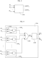
- Figure 4 shows an embodiment of the implementation of the reset circuit 116a.
- the reset circuit 116a receives again a plurality of reset-request signals RT, which are generated by various circuits, such as a processing core 102 or a fault collection and error management circuit 120.
- the reset circuit 116a is configured to generate one or more combined reset-request signals CRT as a function of the reset-request signals RT.
- a combined reset-request signal CRT is generated via a combinational logic circuit 1166 configured to:
- the combinational logic circuit 1166 may be implemented with a logic OR gate.
- the reset circuit 116a is configured to selectively enable or disable one or more (and possibly all) reset-request signals RT.
- a reset-request signal RT may be provided to a logic gate 1162 configured to mask or unmask the respective reset-request signal RT when a respective masking signal TE has a given logic level.
- the combinational logic circuit 1162 may be implemented with a logic AND gate receiving at input a given reset-request signal RT and the respective masking signal TE.
- one or more (and possibly all) reset-request signals RT may be synchronized via a respective synchronization circuit 1164, e.g., implemented via a flip-flop or a plurality of flip-flops connected in cascade.
- a synchronization circuit 1164 is often preferable, because a trigger in a reset-request signal RT may be generated by a circuit, which might be running with a different clock with respect to the clock used by the reset circuit 116a, which preferably is a safe internal oscillator clock.
- one or more of the reset-request signals RT 1 , ... RT m may be provided to a respective sub-circuit 1160, such as 1160 1 , ... 1160 m , wherein each sub-circuit 1160 may comprise a masking circuit 1162 receiving a respective masking signal, such as masking signal TE 1 , ... TE m , and/or a synchronization circuit 1164.
- each sub-circuit 1160 may comprise a masking circuit 1162 receiving a respective masking signal, such as masking signal TE 1 , ... TE m , and/or a synchronization circuit 1164.
- the position of the masking circuit 1162 and the synchronization circuit 1164 may also be inverted, i.e., the synchronization circuit may synchronize a reset-request signal RT and the masking circuit 1162 may selectively mask the synchronized reset-request signal.
- the reset circuit 116a may be configured to generated a plurality of combined reset-request signal CRT by repeating the sub-circuits 1160 and the combinational logic circuit 1166.
- each reset-request signal RT may have associated a plurality of sub-circuits 1160 wherein each sub-circuits receives a respective masking signal TE.
- the one or more combined reset-request signals CRT are provided to a reset management circuit 1168 configured to generate one or more reset signal RST as a function of the one or more combined reset-request signals CRT.
- the reset management circuit 1168 may be activated when anyone of the (unmasked) reset-request signals RT is asserted, e.g., is set to high.
- the system reset signal RST may correspond to a combined reset-request signal CRT, or the reset management circuit 1168 may be implemented with a combinational logic circuit configured to generate the system reset signal RST as a function of one or more of the combined reset-request signals CRT.
- the reset circuit 116a and in particularly the reset management circuit 1168, is configured to generate a plurality of reset signals RST 1 , ..., RST p , wherein the reset circuit selectively asserts and de-asserts one or more of the reset signals RST 1 , ..., RST p according to a given and usually predetermined sequence.
- the reset management circuit 1168 may be implemented with a sequential logic circuit implementing a finite state machine configured to control a sequence of operations.
- the processing system in order to verify the operation of the reset circuit 116a, is configured to verify one or more of (and preferably all):
- the processing system is also configured to verify at least one of:
- processing system may be configured to remain after a power-on in a wait state until a reset is received. Accordingly, in this case, the processing system, in particular the processing cores 102, would not be started when the reset management circuit 1168 of the connectivity to the circuits to be reset is not working correctly.
- test of the reset management circuit 1168 and of the connectivity to the circuits to be reset may be considered covered implicitly by testing the connection to the reset circuit 116a, the operation of the combinational logic circuit 1166 and optionally the sub-circuits 1160.
- the operation of the processing system may be monitored via an external watchdog timer, e.g., forming part of a further processing system configured to monitor the operation of an electronic system comprising a plurality of processing systems (see also Figure 1 ).
- the processing system would not signal the completion of the initialization of the processing system to the watchdog timer (e.g., by asserting a given signal provided to the watchdog timer via software instructions executed by a processing core 102). Accordingly, the external watchdog timer will detect the malfunction of the processing system. For example, in this case, the further processing system may deactivate one or more functionalities at system level and/or may report a malfunction of the processing system.
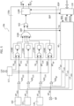
- FIG. 5 shows an embodiment of a processing system 10a according to the present disclosure.
- the processing system 10a comprises again a reset circuit 116a configured to receive a plurality of reset-request signals RT.
- a first reset-request signal RT 115 is generated by a power supply monitoring circuit 115 configured to monitor a supply voltage of the processing system 10a.
- the power supply monitoring circuit 115 may comprise for this purpose a comparator, e.g., a comparator with hysteresis, i.e., a Schmitt trigger, configured to compare the supply voltage with one or more threshold values. Accordingly, in this way, the signal RT 115 may request a reset of the processing system 10a when the processing system 10a is switched on.
- further reset-request signals RT may be provided by other circuits, such as IP cores, of the processing system 10a.
- one or more second reset-request signals RT 102 may be provided by each processing core 102 of the processing system 10a.
- a reset-request signal RT 102 may be asserted via software instructions executed by the respective microprocessor 1020.
- one or more reset-request signals RT 120 may be provided by fault collection and error management circuit 120.
- a reset-request signal RT 120 may be asserted in case of a malfunction signaled via one or more error signals ERR (see the description of Figure 2 ).
- one or more reset-request signals RT RP may be provided by one or more respective terminals RP of the processing system 10a, such as pins or pads of a respective integrated circuit comprising the processing system, in particular the circuits 102, 115, 116a, 120.
- the reset circuit 116a receives thus the signals RT, e.g., the signals RT 102 , RT 115 , RT 120 and RT RP .
- each reset signal RT is then provided to a respective sub-circuit 1160 of the reset circuit 116a.
- the sub-circuits, and the respective masking circuit 1162 and/or synchronization circuit 1164 are purely optional.
- each of the reset-request signals RT 102 , RT 120 and RT RP may be provided to a respective sub-circuit 1160 comprising at least the synchronization circuit 1160, and preferably also the masking circuit 1162.
- the sub-circuit 1160 for the reset-request signal RT 115 generated by the power supply monitoring circuit 115 may be omitted or may only comprise the synchronization circuit 1164, i.e., the reset-request signal RT 115 may not be masked, because usually such a reset in response to a power-on of the processing system 10a is necessary.
- the masking signals TE such as signals TE 102 , TE 120 and TE RP , may be provided by a circuit 117.
- the circuit may be a register interface connected to the communication system 114, which thus permits that the logic levels of the masking signals TE (or at least a subset thereof) may be programmable, e.g., via software instructions executed by a processing core 102.
- the processing system 10a is configured to test the whole chain from the generation of the reset-request signals RT till the output of the combinational logic circuit 1166 configured to generate a combined reset-request signal CRT.
- the processing system 10a comprises for this purpose a test circuit, configured to execute a Reset Built-In Self-Test, also identified as R-BIST in the following.
- the test circuit comprises a control circuit 40, e.g., a hardware sequential logic circuit implementing an FSM, which sequentially asserts one reset-request signals RT at a time and validates the correctness of the combined reset-request signal(s) CRT after the combinational logic circuit(s) 1166.
- a respective combinational logic circuit 420 configured to selectively assert the respective reset-request signal RT as a function of a respective (connectivity) test signal CT.
- a respective (connectivity) test signal CT For example, in Figure 5 are shown combinational logic circuits 420 102 , 420 115 , 420 120 and 420 RP and respective test signals CT 102 , CT 115 , CT 120 and CT RP for the reset quests signal RT 102 , RT 115 , RT 120 and RT RP .
- each combinational logic circuit 420 may be implemented with a logic OR gate, whereby the reset-request signal is asserted when the respective test signal CT is set to high.
- the combinational logic circuit 420 may not be provided for all reset-request signals RT.
- the combinational logic circuit 420 115 for the reset-request signal RT 115 may be omitted, because the processing system 10a would never be started when this reset-request signal RT 115 would not work correctly.
- the modified reset-request signal RT' is generated prior to the transmission via the lines within the integrated circuit, i.e., the distance between the circuit 420 and the respective circuit generating the reset-request signal RT is smaller than the distance between the circuit 4200 and the reset circuit 116a.
- the reset circuit 116a is configured to receive the reset-request signals RT' (instead of the original reset-request signals RT).
- each combinational logic circuit 420 is provided at the output of the respective circuit generating respective the reset-request signal RT and may also be integrated within the respective circuit, e.g .:
- the circuits 420 may be used to generate a modified reset-request signal RT', e.g., modified reset-request signals RT' 102 , RT' 115 , RT' 120 and RT' RP , by selectively asserting the original reset-request signals RT 102 , RT 115 , RT 120 and RT RP via the test signals CT 102 , CT 115 , CT 120 and CT RP .
- the combinational logic circuit 420 may also not be provided for all reset-request signals RT.
- the reset circuit 116a comprises also an additional masking circuit 422 configured to selectively mask or unmask the combined reset-request signal(s) CRT when a test mode signal TM is asserted.
- additional masking circuit 422 may be implemented with a logic AND gate.
- the test signals CT such as CT 102 , CT 115 , CT 120 and CT RP , and the test mode signal TM are generated/provided by the control circuit 40. Moreover, the control circuit 40 monitors the combine reset-request signal(s) CRT.
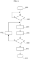
- Figure 6 shows an embodiment of the operation of the test circuit, in particular the control circuit 40.
- control circuit 40 waits at a step 1002 until a test of the reset circuit 116a is requested.
- the test may be requested via software and/or via hardware.
- the control circuit 40 may be connected to the communication system 114.
- a microprocessor 1020 of a processing core 102 may generate the respective test request via software instructions, wherein the test request is then transmitted to the control circuit 40 via the communication system 114.
- the test request is then transmitted to the control circuit 40 via the communication system 114.
- the control circuit 40 may be requested one or more tests with different values for the masking signals TE, which thus permits to verify also the operation of the masking circuits 1162.
- the inventors have observed that such a software-controlled test is usually not advisable.
- the combined reset-request signal(s) CRT are masked during the test. Accordingly, this masking would also mask a real reset-request occurring during the test.
- the test is requested directly in hardware as part of a Build-In Self-Test (BIST) of the processing system 10a, which is executed while the microprocessor(s) 1020 are not started yet.
- BIST Build-In Self-Test
- the processing system 10a may comprise a diagnostic circuit 118 implementing a BIST control circuit.
- the processing system 10a in response to switching on the processing system 10a, i.e., in response to one or more of the reset-request signals RT, the processing system 10a may be configured to execute the following phases in sequence during a (complex) reset procedure:
- a microprocessor 1020 may be reset by asserting the respective reset signal RST 102 and the microprocessor 1020 may be started by de-asserting the respective reset signal RST 102 . Accordingly, in this case, the reset signal RST 102 may be asserted during the first reset phase, the diagnostic phase, and the optional second reset phase.
- one or more circuits of the processing system 10a may be kept under reset (by asserting the respective reset signal RST) during the diagnostic phase, such as the processing core(s) 102 and most (or all) of the resources/peripherals 106, while one or more other circuits may be active ( e.g ., with the respective reset signal RST being de-asserted) during the diagnostic phase, such as the memory controller 110, the diagnostic circuit 118 and the fault collection and error management circuit 120.
- a state control circuit e.g., implemented within the FSM 1168, may thus automatically request the execution of one or more build-in self-test operations during the reset procedure. Accordingly, in this case, the test may be requested as part of these BIST operation.
- the reset management circuit 1168 is configured to provide a signal SDP to the diagnostic circuit 118, wherein the reset management circuit 1168 asserts the signal SDP in order to start the diagnostic phase, i. e., request the execution of the BIST.
- the diagnostic circuit 118 starts then one or more tests.
- the diagnostic circuit 118 provides a signal SRD to the control circuit 40, wherein the diagnostic circuit 118 asserts the signal SRD in order to request the start of the test of the reset circuit 116a, i.e., the control circuit 40 determines at the step 1002 whether the signal SRD is asserted.
- the control circuit 40 may assert a signal ERD in order to indicate the completion of the test, and provide a signal STATE indicating the result of the tests. Accordingly, once all tests have been executed, e.g., in response to the signal ERD, the diagnostic circuit 118 may assert a signal EDP in order to indicate the end of the diagnostic phase. In response to the signal EDP, the reset management circuit 1168 may thus execute the second reset phase and/or start the microprocessor(s) 1020.
- the diagnostic circuit 118 does not provide the result of the test to the reset management circuit 1168, but the result (such as the signal STATE) is used to generate an error signal provided to the fault collection and error management circuit 120 and/or the diagnostic circuit 118 is connected to the communication system 114, whereby a microprocessor 1020 may read the result(s) of the diagnostic phase by sending read requests to the communication system 114.
- the operation of the diagnostic circuit 118 could also be implemented directly within the reset circuit 116a, e.g., within the reset management circuit 1168.
- control circuit 40 returns to the step 1002. Conversely, in case a test has been requested (output "Y” of the verification step 1002), the control circuit 40 proceeds to a step 1004 where the control circuit 40 sets the signal TM ( e.g ., to low) in order to mask the combined reset-request signal(s) CRT and asserts one of the test signals CT, thereby asserting the respective reset-request signals RT'.
- TM e.g ., to low
- control circuit 40 evaluates then the logic level of the combined reset-request signal(s) CRT.
- the control circuit 40 may be configured to compare at the step 1006 each combined reset-request signal CRT with a respective expected value. For example, assuming that a combined reset-request signal CRT is generated by combining all reset-request signals RT (or more specifically the received reset-requests signals RT'), the combined reset-request signal CRT should be asserted at the step 1006.
- the control circuit 40 may set the signal STATE to indicate a (general) failure of the reset circuit 116a and/or a (specific) failure of the currently asserted test signal CT, and thus the respect reset-request signal RT.
- the control circuit 40 may then verify whether all test signals CT have been tested. In case not all test signals CT have been tested (output "N" of the verification step 1008), the control circuit 40 selects at a step 1010 a next test signal CT and returns to the step 1004, where the control circuit 40 asserts then the selected test signal CT, and de-asserts all other test signals CT, thereby asserting only the respective reset-request signal RT'.
- control circuit 40 sets the signal TM (e.g., to high) in order to unmask the combined reset-request signal(s) CRT, and the operation stops at a stop step 1014.
- control circuit 40 may also signal the completion of the test at the step 1012, e.g., by asserting the completion signal ERD for the diagnostic circuit 118.
- the test circuit 40, 420, 422 sequentially asserts one of the reset-request signal RT'.
- the control circuit 40 waits for one or more clock cycles, in order to ensure that the logic level of the reset-request signal RT' may be propagated to the combined reset-request signal(s) CRT.
- the control circuit 40 may acquire and/or verify the logic level of the combined reset-request signal(s) CRT, e.g., in order to verify whether the reset event has been propagated correctly to the output of the combinational logic circuit 1166.
- the reset event does not generate an actual reset, because the combined reset-request signal(s) CRT are masked via the masking circuit 422 and the test-mode signal TM.
- no additional circuits may be provided in order to test the correct functionality of the masking circuit 422.
- the correct functionality of this masking gate 422 is implicitly granted by two facts:
- control circuit 40 may be used to also verify the reset signals RST used to reset individual circuits/IPs.
- Figure 7 shows an embodiment of the connection of the reset circuit 116a, in particular the reset management circuit 1168, to a plurality of circuits.
- the reset management circuit 1168 generates a plurality of p reset signals, wherein:
- RST may be provided to other circuits of the processing system 10a, such as a DMA controller 110 and the fault collection and error management circuit 120.
- each reset signal RST is provided to the respective circuit via an optional synchronization circuit 1170, such as synchronization circuit 1170 1 , ..., 1170 p , e . g ., implemented via one or more flip-flops connected in cascade.
- an optional synchronization circuit 1170 such as synchronization circuit 1170 1 , ..., 1170 p , e . g ., implemented via one or more flip-flops connected in cascade.
- each circuit provides one or more reset-status signal RSTAT, e.g., reset-status signal RSTAT 1 , ..., RSTAT p , which indicate whether the respective device has received the reset-requests and/or is executing a reset.
- RSTAT reset-status signal
- the processing system 10a may monitor the respective reset-status signals RSTAT.
- the reset circuit 116 in particular the reset management circuit 1168 may be configured to assert the reset signals RST in response to the reset-request signals RT.
- these signals RT may signal system reset-requests, wherein the reset management circuit 1168 asserts and de-asserts the reset signals RST according to a predetermined sequence.
- the reset management circuit 1168 may assert the reset signals RST almost contemporaneously and then de-assert the reset signals RST according to a given sequency, whereby the respective circuits are started in sequence.
- reset management circuit 1168 may assert and de-assert a respective sub-set of the reset signals RST according to a respective predetermined sequence.
- control circuit 40 may be configured to automatically monitor the signals RSTAT during the reset procedure, e.g., in response to a power-on reset RST 115 of the processing system 10a, because in this case, all status signals RSTAT should signal that the respective circuit has received the reset-request signaled via the respective reset signal RST.
- circuits such as the processing core(s) 102 and the peripherals 106
- the processing core(s) 102 and the peripherals 106 are under reset also during the diagnostic/BIST phase.
- other circuits may not be under reset during the diagnostic phase.
- these circuits such as the memory controller 100, the BIST controller 118, and the fault collection and error management circuit 120, are essential for the operation of the processing system 10a, i.e., the microprocessor(s) 1020 would not start if these circuits do not operate correctly, and/or these circuits may be tested separately.
- the control circuit 40 may also verify whether the reset-status signals RSTAT of these circuits are asserted, e.g., by generating a combined reset-status signal CRSTAT, e.g., via a logic AND gate 1072, indicating whether all the respective reset-status signals RSTAT are asserted. Accordingly, in various embodiments, the control circuit 40 may be configured to just verify the logic level of the combined reset-status signal CRSTAT associated with the circuits, which should be under reset during the diagnostic phase, i.e., the circuits for which the respective reset signal RST is asserted during the diagnostic phase.
- reset operations of individual circuits are typically not managed via reset-request signals RT, but by selectively asserting one or more of the reset signals RST via software instructions executed by a micro-processor 1020.
- the reset management circuit 1168 may comprise or have associated a register interface, e.g., the register interface 117, used to set the logic level of one or more (and preferably all) reset signals RST, and optionally in order to read the logic level of the reset-status signals RSTAT.
- a micro-processor 1020 may verify the connectivity of a given reset signal RST by asserting the respective reset signal RST and verifying the respective reset-status signals RSTAT. Additionally or alternatively, the reset-status signals RSTAT may also in this case be provided to the control circuit 40. For example, the control circuit 40 may monitor the reset signals RST, determine whether one or more of these reset signals RST are asserted, and then determine whether the one or more reset-status signals RSTAT provided by the circuits having the reset signal asserted is also asserted.
- the control circuit 40 may signal a failure, e.g., via an error signal ERR provided to the fault collection and error management circuit 120 and/or an interrupt provided to the processing core(s) 102.
- one or more of the embodiments disclosed herein provide solutions for testing the logic and associated signals used to request and generate a reset, covering both system resets reset and individual reset signals.
- the described solution may be executed in hardware, with a minimal execution time, minimal area overhead, and no software intervention.
- the reset generation logic can be at ASIL-D level.
Landscapes
- Engineering & Computer Science (AREA)
- Theoretical Computer Science (AREA)
- General Engineering & Computer Science (AREA)
- Physics & Mathematics (AREA)
- General Physics & Mathematics (AREA)
- Quality & Reliability (AREA)
- Computer Hardware Design (AREA)
- Debugging And Monitoring (AREA)
Abstract
Description
- Embodiments of the present disclosure relate to the error management within processing systems, such as micro-controllers.
-
Figure 1 shows a typical electronic system, such as the electronic system of a vehicle, comprising a plurality ofprocessing systems 10, such as embedded systems or integrated circuits, e.g., a Field Programmable Gate Array (FPGA), a Digital Signal Processor (DSP) or a micro-controller (e.g., dedicated to the automotive market). - For example, in
Figure 1 are shown threeprocessing systems suitable communication system 20. For example, the communication system may include a vehicle control bus, such as a Controller Area Network (CAN) bus, and possibly a multimedia bus, such as a Media Oriented Systems Transport (MOST) bus, connected to vehicle control bus via a gateway. Typically, theprocessing systems 10 are located at different positions of the vehicle and may include, e.g., an Engine Control Unit, a Transmission Control Unit (TCU), an Anti-lock Braking System (ABS), a Body Control Module (BCM), and/or a navigation and/or multimedia audio system. Accordingly, one or more of theprocessing systems 10 may also implement real-time control and regulation functions. These processing systems are usually identified as Electronic Control Units. - In this respect, future generation of
such processing systems 10, e.g., micro-controllers adapted to be used in automotive applications, are expected to exhibit an increase in complexity, mainly due to the increasing number of requested functionalities (new protocols, new features, etc.) and to the tight constraints of execution conditions (e.g., lower power consumption, increased calculation power and speed, etc.). For example, recently more complexmulti-core processing systems 10 have been proposed. For example, such multi-core processing systems may be used to execute (in parallel) several of theprocessing systems 10 shown inFigure 1 , such as several ECUs of a vehicle. -
Figure 2 shows an example of aprocessing system 10, such as a multi-core processing system. Specifically, in the example considered, theprocessing system 10 comprises one ormore processing cores 102, such as a plurality ofn processing cores 1021...102n, connected to a (on-chip)communication system 114. For example, in the context of real-time control systems, theprocessing cores 1021...102n may be ARM Cortex®-R52 cores. Generally, thecommunication system 114 may comprise one or more bus systems, e.g., based on the Advanced eXtensible Interface (AXI) bus architecture, and/or a Network-on-Chip (NoC). - For example, as shown at the example of the
processing core 1021, eachprocessing core 102 may comprise amicroprocessor 1020 and acommunication interface 1022 configured to manage the communication between themicroprocessor 1020 and thecommunication system 114. Typically, theinterface 1022 is a master interface configured to forward a given (read or write) request from themicroprocessor 1020 to thecommunication system 114, and forward an optional response from thecommunication system 114 to themicroprocessor 1020. However, thecommunication interface 1022 may also comprise a slave interface. For example, in this way, afirst microprocessor 1020 may send a request to a second microprocessor 1020 (via thecommunication interface 1022 of the first microprocessor, thecommunication system 114 and thecommunication interface 1022 of the second microprocessor). Generally, each processingcore 1021...102n may also comprise further local resources, such as one or morelocal memories 1026, usually identified as Tightly Coupled Memory (TCM). - Typically, the
processing cores 102 are arranged to exchange data with one or morenon-volatile memories 104 and/or one or morevolatile memories 104b. Generally, thememories 104 and/or 104b may be integrated with theprocessing cores 102 in a single integrated circuit, or thememories 104 and/or 104b may be in the form of a separate integrated circuit and connected to theprocessing cores 102, e.g., via the traces of a printed circuit board. - Specifically, in a
multi-core processing system 10 these memories are often system memories, i.e., shared for theprocessing cores 1021...102n. For example, for this purpose, the communication with thememories 104 and/or 104b may be performed via one ormore memory controllers 100 connected to thecommunication system 114. As mentioned before, eachprocessing cores 102 may, however, comprise one or more additionallocal memories 1026. - For example, the software executed by the microprocessor(s) 1020 is usually stored in a
non-volatile program memory 104, such as a Flash memory or EEPROM, i.e., thememory 104 is configured to store the firmware of theprocessing unit 102, wherein the firmware includes the software instructions to be executed by themicroprocessor 102. Generally, thenon-volatile memory 104 may also be used to store other data, such as configuration data, e.g., calibration data. Conversely, avolatile memory 104b, such as a Random-Access-Memory (RAM), may be used to store temporary data. - Often, the
processing system 10 comprises also one or more (hardware) resources/peripherals 106, e.g., selected from the group of: - one or more communication interfaces, e.g., for exchanging data via the
communication system 20, such as a Universal asynchronous receiver/transmitter (UART), Serial Peripheral Interface Bus (SPI), Inter-Integrated Circuit (I2C), Controller Area Network (CAN) bus, and/or Ethernet interface, and/or a debug interface; and/or - one or more analog-to-digital converters and/or digital-to-analog converters; and/or
- one or more dedicated digital components, such as hardware timers and/or counters, or a cryptographic co-processor; and/or
- one or more analog components, such as comparators, sensors, such as a temperature sensor, etc.; and/or
- one or more mixed signal components, such as a PWM (Pulse-Width Modulation) driver.
- Generally, a dedicated digital component may also correspond to a FPGA integrated in the
processing system 10. For example, in this case, thememory 104 may also comprise the program data for such a FPGA. - The
resources 106 are usually connected to thecommunication system 114 via arespective communication interface 1062, such as a peripheral bridge. For example, for this purpose, thecommunication system 114 may indeed comprise an Advanced Microcontroller Bus Architecture (AMBA) High-performance Bus (AHB), and an Advanced Peripheral Bus (APB) used to connect the resources/peripherals 106 to the AMBA AHB bus. In general, thecommunication interface 1062 comprises at least a slave interface. For example, in this way, aprocessing core 102 may send a request to aresource 106 and the resource returns given data. Generally, one or more of thecommunication interfaces 1062 may also comprise a respective master interface. For example, such a master interface, often identified as integrated Direct Memory Access (DMA) controller, may be useful in case the resource has to start a communication in order to exchange data via (read and/or write) request with another circuit connected to thecommunication system 114, such as aresource 106 or aprocessing core 102. - Often
such processing systems 10 comprise also one or more general-purpose DMA controllers 110. For example, as shown inFigure 2 , aDMA controller 110 may be used to directly exchange data with a memory, e.g., thememory 104b, based on requests received from aresource 106. For example, in this way, a communication interface may directly read data (via the DMA controller 110) from thememory 104b and transmit these data, without having to exchange further data with aprocessing unit 102. Generally, aDMA controller 110 may communicate with the memory or memories via thecommunication system 114 or via one or more dedicated communication channels. - In this respect, irrespective of the complexity of the processing system 10 (e.g., with respect to the number of
processing cores 102 and/or number and type of the resources 106), a typical processing system comprises also areset circuit 116. - For example, such as
reset circuit 116 may be configured to receive one or more reset-request signals RT, such as signal RT1, ..., RTm, indicating a given event. For example, each of the reset-request signals RT may be selected from the group of: - a reset-request signal provided by a power supply monitoring circuit of the
processing system 10, wherein the power supply monitoring circuit asserts the reset-request signal RT when the supply voltage of theprocessing system 10a has been switched on; - a reset-request signal provided by a respective reset terminal, such as pins or pads of a respective integrated circuit comprising the
processing system 10; - a reset-request signal RT102 provided by a
processing core 102, in particular arespective microprocessor 1020 configured to assert the respective reset-request signal RT102 via software instructions. - Often one or more reset-request signals RT120 may also be provided by a fault collection and
error management circuit 120. For example, such a fault collection anderror management circuit 120 may received one or more error signal ERR, such as error signals ERR1, ..., ERRk, and selectively assert a reset-request signals RT120 as a function of the error signals ERR1, ..., ERRk. For example, each error signals ERR may correspond to an error signal ERR100 provided by amemory controller 100, an error signal ERR102 provided by aprocessing core 102, an error signal ERR106 provided by aresource 106 and/or an error signal ERR110 provided by a DMA controller. For example, European patent application n.EP 3 534 261 A1 orItalian patent application n. 102021000009683 error management circuit 120, which are incorporated herein by reference for this purpose. - In response to the reset-request signals RT, the
reset circuit 116 asserts then one or more reset signals RST, such as reset signal RST1, ..., RSTp. For example: - each
memory controller 100 may receive a respective reset signal RST100; and/or - each
processing core 102 may receive a respective reset signal RST102; and/or - each
resource 106 may receive a respective reset signal RST106; and/or - each
DMA controller 110 may receive a respective reset signal RST110; and/or - the fault collection and
error management circuit 120 may receive a reset signal RST120. - Generally, the reset may be applied to the
whole processing system 10 or individual circuits of the processing system, so called IPs. For example, in order to generate a system reset of the processing system, thereset circuit 116 may assert all reset signals RST contemporaneously or according to a given sequence. Conversely, in order to generate a reset of an individual circuit or a group of circuits, thereset circuit 116 may assert the respective reset signals RST. For example, in response to the reset signal RST, the respective circuit usually resets one or more (and typically all) registers of the respective circuit, thereby bringing the respective circuit in a predetermined condition. - The inventors have observed that for both cases it is particularly relevant to ensure that the reset is properly applied with time coherency, e.g., in order to avoid that the reset logic and associated signals have some malfunction causing no reset to be generated.
- For example, in the context of the ISO26262 specification for safety in automotive products, a missed reset generation could be catastrophic. In fact, the ISO26262 specification dictates that, in case of error (as managed by the fault collection and error management circuit 120), within a certain scheduled time the
processing system 10, such as a microcontroller, shall be able to enter a safe state. The concept and definition of safe state usually depend on the safety architecture of theprocessing system 10, but at least one case of safe state is usually always applicable: when theprocessing system 10 is under reset, it should be in a safe state. Therefore, one way, compliant with ISO26262 specification, to resolve a critical error is to trigger a reset as reaction upon an error, because in this way theprocessing system 10 should enter a safe state. - The inventors have observed that the above operation implies that that also the proper functionality of the
circuit 116 that intercepts the reset-requests RT and consequently generates one or more reset signals RST should be ensured. - In view of the above, various embodiments of the present disclosure provide solutions for verifying the correct operation of a reset circuit of a processing system.
- According to one or more embodiments, one or more of the above objectives is achieved by means of a processing system having the features specifically set forth in the claims that follow. Embodiments moreover concern a related integrated circuit, device and method.
- The claims are an integral part of the technical teaching of the disclosure provided herein.
- As mentioned before, various embodiments of the present disclosure relate to a processing system, in particular a micro-controller. Specifically, the processing system comprises at least one processing core comprising a microprocessor configured to execute software instructions, a memory controller configured to read the software instructions from a non-volatile memory and a communication system for connecting the memory controller to the processing core. In order to start the processing system, the processing system comprises a power-supply monitoring circuit configured to generate a reset-request signal when the processing system is switched on and the voltage is above a certain power-on voltage threshold, which ensures the correct functionality of the reset start-up phase of the processing system. Accordingly, a reset circuit may receive the reset-request signal and generate a reset of the processing system in response to the reset-request signal.
- For example, in various embodiments, the processing core is configured to be reset in response to a reset signal. However, in various embodiments, the processing system comprises also one or more further circuits configured to be reset in response to a respective further reset signal, and the reset circuit receives also one or more further reset-request signals provided by the processing core, the one or more further circuits and/or a terminal of the processing system. For example, the one or more further circuits configured to be reset in response to a respective reset signal may comprise one or more resources or peripherals, wherein each resource or peripherals is configured to be reset in response to a respective reset signal. Conversely, the one or more further reset-request signals may comprise at least one of: a reset-request signal generated by the microprocessor via software instructions; a reset-request signal generated by a fault collection and error management circuit as a function of one or more error signals received from the memory controller, the processing core and/or a resource or peripherals of the processing system; and a reset-request signal received via a terminal of the processing system.
- In various embodiments, the reset circuit may thus generate a combined reset-request signal by combining the various reset-request signals and activate the reset procedure in response to the combined reset-request signal. For example, the reset circuit may assert the combined reset-request signal when at least one of the reset-request signals is asserted, and de-assert the combined reset-request signal when the reset-request signals are de-asserted.
- Specifically, in various embodiments, in response to the combined reset-request signal, the processing system is configured to execute the following phases in sequence:
- a reset phase, where the reset circuit executes a reset of the processing system by generating the reset signal for the processing core and the further reset signals for the one or more further circuits;
- a diagnostic phase, where a diagnostic circuit executes one or more tests of the processing system; and
- a software runtime phase, where the microprocessor is started and executes the software instruction.
- For example, for this purpose, the reset circuit may be configured to, in response to the combined reset-request signal, execute the reset of the processing system by asserting the reset signal for the processing core and the further reset signals for the one or more further circuits. Generally, during this phase, the reset circuit may also de-assert one or more reset signals. However, in various embodiments, at least the reset signal of the processing core is maintained asserted.
- Once having completed the reset phase, the reset circuit may then generate a signal indicating the start of the diagnostic phase. Accordingly, in response to the signal indicating the start of the diagnostic phase, the diagnostic circuit may execute the one or more tests of the processing system, and generate a signal indicating the end of the diagnostic phase. Accordingly, in response to the signal indicating the end of the diagnostic phase, the reset circuit may start the software runtime phase. For example, for this purpose the reset circuit may de-assert the reset signals according to a predetermined sequence, thereby starting the microprocessor and the further circuit.
- In various embodiments, the reset circuit may comprise for each further reset-request signals a respective masking circuit configured to mask the respective further reset-request signals as a function of a respective masking signal. For example, the masking signals may be provided by a register interface connected to the communication system.
- In particularly, as mentioned before, various embodiments of the present disclosure relate to solutions for testing the operation of the reset circuit. For this purpose, the processing system comprises a hardware test circuit.
- Specifically, in order to test the connection of the reset-request signals to the reset circuit, the optional masking of the reset-request signals and the generation of the combined reset-request signal, the test circuit comprises for each of the one or more further reset-request signals a respective first combinational circuit configured to selectively assert the respective further reset-request signal, preferably prior to its transmission within the processing system, i.e., the distance between the first combinational circuit and the respective processing core or further circuit is smaller than the distance between the first combinational circuit and the reset circuit.
- Moreover, in various embodiments, the test circuit comprises a second combinational logic circuit configured to selectively mask the combined reset-request signal, and a control circuit.
- Specifically, in various embodiments, the control circuit is configured to repeat during the diagnostic phase a sequence of operations for each of the further reset-request signals. In particular, in various embodiments, the control circuit masks the combined reset-request signal via the second combinational logic circuit, asserts the respective further reset-request signal and de-asserts all other further reset-request signals. Next, the control circuit determines whether the combined reset-request signal provided to the second combinational logic circuit (i.e., prior to the masking operation) is asserted. Accordingly, in response to determining that the combined reset-request signal is de-asserted, the control circuit may generate a signal indicating a failure of the reset circuit. For example, this signal may be provided to the diagnostic circuit.
- In various embodiments, the control circuit may also test the connectivity of the reset signals. Specifically, as mentioned before, during the diagnostic phase may still be asserted one or more of the reset signals. Accordingly, by using a processing core and further circuits configured to assert a respective reset-status signal when the circuit is under reset, the control circuit may be configured to monitor the reset-status signals of the circuit, which should be under reset during the diagnostic phase. For example, for this purpose, the control circuit may generate a combined reset-status signal by combining (at least a sub-set of) the reset-status signals, determine whether the combined reset-status signal is asserted, and generate an error signal when the combined reset-status signal is de-asserted.
- Embodiments of the present disclosure will now be described with reference to the annexed drawings, which are provided purely by way of non-limiting example and in which:
-
Figure 1 shows an example of an electronic system comprising a plurality of processing systems; -
Figure 2 shows an examples of processing systems; -
Figure 3 shows a block diagram of a reset circuit; -
Figure 4 shows an embodiment of the reset circuit ofFigure 3 ; -
Figure 5 shows an embodiment of a processing system comprising a reset circuit and a test circuit; -
Figure 6 shows an embodiment of the operation of the test circuit; and -
Figure 7 shows an embodiment of the connection of the reset circuit ofFigure 5 to a plurality of circuits. - In the following description, numerous specific details are given to provide a thorough understanding of embodiments. The embodiments can be practiced without one or several specific details, or with other methods, components, materials, etc. In other instances, well-known structures, materials, or operations are not shown or described in detail to avoid obscuring aspects of the embodiments.
- Reference throughout this specification to "one embodiment" or "an embodiment" means that a particular feature, structure, or characteristic described in connection with the embodiment is included in at least one embodiment. Thus, the appearances of the phrases "in one embodiment" or "in an embodiment" in various places throughout this specification are not necessarily all referring to the same embodiment. Furthermore, the particular features, structures, or characteristics may be combined in any suitable manner in one or more embodiments.
- The headings provided herein are for convenience only and do not interpret the scope or meaning of the embodiments.
- In the following
Figures 3 to 7 parts, elements or components which have already been described with reference toFigures 1 to 2 are denoted by the same references previously used in such Figure; the description of such previously described elements will not be repeated in the following in order not to overburden the present detailed description. - As mentioned before, various embodiments of the present disclosure provide solutions for verifying the correct operation of a reset circuit of a processing system. For a general description of a processing system comprising such a reset circuit may thus be made reference to the previous description of
Figures 1 to 2 . - Accordingly, various embodiments of the present disclosure provide solutions for validating the operation of a reset circuit, in particularly with respect to the functionality of the reset generation logic and also the connection of the reset-request signals RT, with the target to avoid that a reset-request might be lost because of a possible malfunction.
- Moreover, in various embodiments, the solution may not only verify each reset-request signal RT generated within the processing system, but also the connection of the reset signals RST to the individual circuits.
- Various embodiments of the present disclosure may thus be used to provide a coverage according the ASIL-D level of the ISO26262 specification.
-
Figure 3 shows an embodiment of areset circuit 116a, also called reset generator circuit. Specifically, in the embodiment considered, and as described in the foregoing, thereset circuit 116a is configured to receive at least one reset-request signal RT, such as signals RT1, ..., RTm, and generates at least one reset signal RST, such as signals RST1, ..., RSTp. For example, the reset-request signals RT and/or reset signals RST may be trigger signals, i.e., a signal wherein an event is signaled via a pulse of a given number of clock cycles. - For example, in various embodiments, the
reset circuit 116a may be configured to generate a single system reset signal, which is provided to all circuits receiving a reset signal. - Alternatively, one or more of the circuits, such as the
circuits Figure 2 . For example, in this case, thereset circuit 116a may be implemented with a sequential logic circuit/finite state machine (FSM) configured to generate a system reset by selectively asserting and de-asserting the individual reset signals in sequence. In fact, the reset process of a system reset may comprise a sequence of states, wherein each state is dedicated to a different task, such as an initialization phase for initializing theNVM memory 104, the configuration phase for reading configuration data from theNVM memory 104 and storing these configuration data to registers of the processing system, etc. For example, in this context may be citedItalian Patent Application n. 102021000007871 - Accordingly, the use of individual reset signal RST has the advantage that the reset signals RST may be used to activate or de-activate the reset of several IPs at precise moments during the evolution of the reset sequence.
- Moreover, by using individual reset signals RST one or more of the circuits may also be reset during the run-time of the processing system, e.g., a
resource 106 may be reset while the processing core(s) 102 are not reset. Accordingly, in order to resolve local malfunctions of a given circuit without the need of a global system reset, the respective circuit may be reset while the micro-processor(s) 1020 are still executing software instruction. - Generally, the following solutions for testing the
reset circuit 116a could be used in both cases, i.e., when the reset signal or the reset signals RST generated by thereset circuit 116a comprise a common system reset signal and/or a plurality of individual reset signals. -
Figure 4 shows an embodiment of the implementation of thereset circuit 116a. - In the embodiment considered, the
reset circuit 116a receives again a plurality of reset-request signals RT, which are generated by various circuits, such as aprocessing core 102 or a fault collection anderror management circuit 120. - In the embodiment considered, the
reset circuit 116a is configured to generate one or more combined reset-request signals CRT as a function of the reset-request signals RT. For example, in various embodiments, a combined reset-request signal CRT is generated via acombinational logic circuit 1166 configured to: - assert the combined reset-request signal CRT when at least one of the reset-request signal RT is asserted; and
- de-assert the combined reset-request signal CRT when all reset-request signals RT are de-asserted.
- For example, assuming that the reset-request signals RT and the combined reset-request signal CRT are asserted when the respective signal is set to high, the
combinational logic circuit 1166 may be implemented with a logic OR gate. - In various embodiments, the
reset circuit 116a is configured to selectively enable or disable one or more (and possibly all) reset-request signals RT. For example, for this purpose, a reset-request signal RT may be provided to alogic gate 1162 configured to mask or unmask the respective reset-request signal RT when a respective masking signal TE has a given logic level. For example, assuming that a reset-request signal RT is asserted when the signal is set to high and the signal should be masked when the masking signal TE is set to low, thecombinational logic circuit 1162 may be implemented with a logic AND gate receiving at input a given reset-request signal RT and the respective masking signal TE. - In various embodiments, one or more (and possibly all) reset-request signals RT may be synchronized via a
respective synchronization circuit 1164, e.g., implemented via a flip-flop or a plurality of flip-flops connected in cascade. Such asynchronization circuit 1164 is often preferable, because a trigger in a reset-request signal RT may be generated by a circuit, which might be running with a different clock with respect to the clock used by thereset circuit 116a, which preferably is a safe internal oscillator clock. - Accordingly, in various embodiments, one or more of the reset-request signals RT1, ... RTm, may be provided to a respective sub-circuit 1160, such as 11601, ... 1160m, wherein each sub-circuit 1160 may comprise a
masking circuit 1162 receiving a respective masking signal, such as masking signal TE1, ... TEm, and/or asynchronization circuit 1164. Generally, the position of themasking circuit 1162 and thesynchronization circuit 1164 may also be inverted, i.e., the synchronization circuit may synchronize a reset-request signal RT and themasking circuit 1162 may selectively mask the synchronized reset-request signal. - In various embodiments, the
reset circuit 116a may be configured to generated a plurality of combined reset-request signal CRT by repeating the sub-circuits 1160 and thecombinational logic circuit 1166. Specifically, in this case, each reset-request signal RT may have associated a plurality of sub-circuits 1160 wherein each sub-circuits receives a respective masking signal TE. - In the embodiment considered, the one or more combined reset-request signals CRT are provided to a
reset management circuit 1168 configured to generate one or more reset signal RST as a function of the one or more combined reset-request signals CRT. For example, in this way, thereset management circuit 1168 may be activated when anyone of the (unmasked) reset-request signals RT is asserted, e.g., is set to high. - For example, when only a single system reset signal RST is used, the system reset signal RST may correspond to a combined reset-request signal CRT, or the
reset management circuit 1168 may be implemented with a combinational logic circuit configured to generate the system reset signal RST as a function of one or more of the combined reset-request signals CRT. - However, as mentioned before, usually, the
reset circuit 116a, and in particularly thereset management circuit 1168, is configured to generate a plurality of reset signals RST1, ..., RSTp, wherein the reset circuit selectively asserts and de-asserts one or more of the reset signals RST1, ..., RSTp according to a given and usually predetermined sequence. Accordingly, in this case, thereset management circuit 1168 may be implemented with a sequential logic circuit implementing a finite state machine configured to control a sequence of operations. - Accordingly, in various embodiments, in order to verify the operation of the
reset circuit 116a, the processing system is configured to verify one or more of (and preferably all): - the connectivity/connection between the circuit generating a reset-request signal RT and the
reset circuit 116a; - the operation of the optional sub-circuits 1160, i.e.:
- a) the masking of the respective reset-request signal RT via the
masking circuit 1162, and/or - b) the synchronization of the respective reset-request signal RT or the respective signal at the output of the
masking circuit 1162 via thesynchronization circuit 1164, and the respective storage of the synchronized signal to a flip-flop; and
- a) the masking of the respective reset-request signal RT via the
- the operation of the
combinational logic circuit 1166 used to generate the combined reset signal CRT. - In various embodiments, the processing system is also configured to verify at least one of:
- the operation of the
reset management circuit 1168; and - the connectivity of the reset signals RST to the respective circuits receiving the reset signals RST.
- However, these additional verifications are purely optional, because the processing system may be configured to remain after a power-on in a wait state until a reset is received. Accordingly, in this case, the processing system, in particular the
processing cores 102, would not be started when thereset management circuit 1168 of the connectivity to the circuits to be reset is not working correctly. - Accordingly, the test of the
reset management circuit 1168 and of the connectivity to the circuits to be reset may be considered covered implicitly by testing the connection to thereset circuit 116a, the operation of thecombinational logic circuit 1166 and optionally the sub-circuits 1160. For example, in case of safety critical applications, the operation of the processing system may be monitored via an external watchdog timer, e.g., forming part of a further processing system configured to monitor the operation of an electronic system comprising a plurality of processing systems (see alsoFigure 1 ). Accordingly, in case the initial reset phase after a power-on would not be started or would not be completed, the processing system would not signal the completion of the initialization of the processing system to the watchdog timer (e.g., by asserting a given signal provided to the watchdog timer via software instructions executed by a processing core 102). Accordingly, the external watchdog timer will detect the malfunction of the processing system. For example, in this case, the further processing system may deactivate one or more functionalities at system level and/or may report a malfunction of the processing system. -
Figure 5 shows an embodiment of aprocessing system 10a according to the present disclosure. - In the embodiment considered, the
processing system 10a comprises again areset circuit 116a configured to receive a plurality of reset-request signals RT. For example, in the embodiment considered, a first reset-request signal RT115 is generated by a powersupply monitoring circuit 115 configured to monitor a supply voltage of theprocessing system 10a. For example, the powersupply monitoring circuit 115 may comprise for this purpose a comparator, e.g., a comparator with hysteresis, i.e., a Schmitt trigger, configured to compare the supply voltage with one or more threshold values. Accordingly, in this way, the signal RT115 may request a reset of theprocessing system 10a when theprocessing system 10a is switched on. - As described in the foregoing, further reset-request signals RT may be provided by other circuits, such as IP cores, of the
processing system 10a. For example, in various embodiments, one or more second reset-request signals RT102 may be provided by eachprocessing core 102 of theprocessing system 10a. For example, in this way, a reset-request signal RT102 may be asserted via software instructions executed by therespective microprocessor 1020. Additionally or alternatively, one or more reset-request signals RT120 may be provided by fault collection anderror management circuit 120. For example, in this case, a reset-request signal RT120 may be asserted in case of a malfunction signaled via one or more error signals ERR (see the description ofFigure 2 ). Additionally or alternatively, one or more reset-request signals RTRP may be provided by one or more respective terminals RP of theprocessing system 10a, such as pins or pads of a respective integrated circuit comprising the processing system, in particular thecircuits - In the embodiment considered, the
reset circuit 116a receives thus the signals RT, e.g., the signals RT102, RT115, RT120 and RTRP. In the embodiment considered, each reset signal RT is then provided to arespective sub-circuit 1160 of thereset circuit 116a. As mentioned before, the sub-circuits, and therespective masking circuit 1162 and/orsynchronization circuit 1164, are purely optional. For example, each of the reset-request signals RT102, RT120 and RTRP may be provided to a respective sub-circuit 1160 comprising at least thesynchronization circuit 1160, and preferably also themasking circuit 1162. Conversely, the sub-circuit 1160 for the reset-request signal RT115 generated by the powersupply monitoring circuit 115 may be omitted or may only comprise thesynchronization circuit 1164, i.e., the reset-request signal RT115 may not be masked, because usually such a reset in response to a power-on of theprocessing system 10a is necessary. - For example, in the embodiment considered, the masking signals TE, such as signals TE102, TE120 and TERP, may be provided by a
circuit 117. For example, the circuit may be a register interface connected to thecommunication system 114, which thus permits that the logic levels of the masking signals TE (or at least a subset thereof) may be programmable, e.g., via software instructions executed by aprocessing core 102. - As described in the foregoing, in various embodiments, the
processing system 10a is configured to test the whole chain from the generation of the reset-request signals RT till the output of thecombinational logic circuit 1166 configured to generate a combined reset-request signal CRT. - In various embodiments, the
processing system 10a comprises for this purpose a test circuit, configured to execute a Reset Built-In Self-Test, also identified as R-BIST in the following. Specifically, as will be described in greater detail in the following the test circuit comprises acontrol circuit 40, e.g., a hardware sequential logic circuit implementing an FSM, which sequentially asserts one reset-request signals RT at a time and validates the correctness of the combined reset-request signal(s) CRT after the combinational logic circuit(s) 1166. - Specifically, in various embodiments, with one or more reset-request signals RT is associated a respective
combinational logic circuit 420 configured to selectively assert the respective reset-request signal RT as a function of a respective (connectivity) test signal CT. For example, inFigure 5 are showncombinational logic circuits combinational logic circuit 420 may be implemented with a logic OR gate, whereby the reset-request signal is asserted when the respective test signal CT is set to high. Generally, thecombinational logic circuit 420 may not be provided for all reset-request signals RT. For example, thecombinational logic circuit 420115 for the reset-request signal RT115 may be omitted, because theprocessing system 10a would never be started when this reset-request signal RT115 would not work correctly. - Specifically, in various embodiments, the modified reset-request signal RT' is generated prior to the transmission via the lines within the integrated circuit, i.e., the distance between the
circuit 420 and the respective circuit generating the reset-request signal RT is smaller than the distance between the circuit 4200 and thereset circuit 116a. Accordingly, in the embodiment considered, thereset circuit 116a is configured to receive the reset-request signals RT' (instead of the original reset-request signals RT). Accordingly, in various embodiments, eachcombinational logic circuit 420 is provided at the output of the respective circuit generating respective the reset-request signal RT and may also be integrated within the respective circuit, e.g.: - the
combinational logic circuit 420102 is provided at the output of (or is integrated in) therespective processing core 102; - the
combinational logic circuit 420115 is provided at the output of (or is integrated in) the powersupply monitoring circuit 115; - the
combinational logic circuit 420120 is provided at the output of (or is integrated in) the fault collection anderror management circuit 120; and - the
combinational logic circuit 420RP is provided at the output of (or is integrated in) the input circuit of the pin or pad RP. - Accordingly, the
circuits 420 may be used to generate a modified reset-request signal RT', e.g., modified reset-request signals RT'102, RT'115, RT'120 and RT'RP, by selectively asserting the original reset-request signals RT102, RT115, RT120 and RTRP via the test signals CT102, CT115, CT120 and CTRP. As mentioned before, thecombinational logic circuit 420 may also not be provided for all reset-request signals RT. - In the embodiment, the
reset circuit 116a comprises also anadditional masking circuit 422 configured to selectively mask or unmask the combined reset-request signal(s) CRT when a test mode signal TM is asserted. For example, assuming that the combined reset-request signa(s) CRT are asserted by setting the signal to high and the combined reset-request signa(s) CRT should be masked when the signal TM is set to low, theadditional masking circuit 422 may be implemented with a logic AND gate. - Accordingly, in the embodiment considered, the test signals CT, such as CT102, CT115, CT120 and CTRP, and the test mode signal TM are generated/provided by the
control circuit 40. Moreover, thecontrol circuit 40 monitors the combine reset-request signal(s) CRT. -
Figure 6 shows an embodiment of the operation of the test circuit, in particular thecontrol circuit 40. - Specifically, after a
start step 1000, thecontrol circuit 40 waits at astep 1002 until a test of thereset circuit 116a is requested. - Generally, the test may be requested via software and/or via hardware. For example, for this purpose, the
control circuit 40 may be connected to thecommunication system 114. For example, in this case, amicroprocessor 1020 of aprocessing core 102 may generate the respective test request via software instructions, wherein the test request is then transmitted to thecontrol circuit 40 via thecommunication system 114. For example, in this way may be requested one or more tests with different values for the masking signals TE, which thus permits to verify also the operation of the maskingcircuits 1162. - However, the inventors have observed that such a software-controlled test is usually not advisable. In fact, as mentioned before, the combined reset-request signal(s) CRT are masked during the test. Accordingly, this masking would also mask a real reset-request occurring during the test. For this reason, in various embodiments, the test is requested directly in hardware as part of a Build-In Self-Test (BIST) of the
processing system 10a, which is executed while the microprocessor(s) 1020 are not started yet. For example, as shown inFigure 5 , in this case, theprocessing system 10a may comprise adiagnostic circuit 118 implementing a BIST control circuit. For example, as described in the previously cited document102021000007871 processing system 10a, i.e., in response to one or more of the reset-request signals RT, theprocessing system 10a may be configured to execute the following phases in sequence during a (complex) reset procedure: - a first reset step, where the
reset circuit 116a executes a first (system) reset of theprocessing system 10a; - a diagnostic phase, where the
diagnostic circuit 118 executes the one or more tests of theprocessing system 10a; - an optional second reset phase, where the
reset circuit 116a executes a second (system) reset of theprocessing system 10a; and - a software runtime phase, where the one or
more microprocessors 1020 are started and execute software instruction. - For example, a
microprocessor 1020 may be reset by asserting the respective reset signal RST102 and themicroprocessor 1020 may be started by de-asserting the respective reset signal RST102. Accordingly, in this case, the reset signal RST102 may be asserted during the first reset phase, the diagnostic phase, and the optional second reset phase. Accordingly, in general, one or more circuits of theprocessing system 10a may be kept under reset (by asserting the respective reset signal RST) during the diagnostic phase, such as the processing core(s) 102 and most (or all) of the resources/peripherals 106, while one or more other circuits may be active (e.g., with the respective reset signal RST being de-asserted) during the diagnostic phase, such as thememory controller 110, thediagnostic circuit 118 and the fault collection anderror management circuit 120. - In various embodiments, a state control circuit, e.g., implemented within the
FSM 1168, may thus automatically request the execution of one or more build-in self-test operations during the reset procedure. Accordingly, in this case, the test may be requested as part of these BIST operation. - For example, this is also shown in
Figure 5 , where thereset management circuit 1168 is configured to provide a signal SDP to thediagnostic circuit 118, wherein thereset management circuit 1168 asserts the signal SDP in order to start the diagnostic phase, i. e., request the execution of the BIST. In response to the signal SDP, thediagnostic circuit 118 starts then one or more tests. For example, in various embodiments, thediagnostic circuit 118 provides a signal SRD to thecontrol circuit 40, wherein thediagnostic circuit 118 asserts the signal SRD in order to request the start of the test of thereset circuit 116a, i.e., thecontrol circuit 40 determines at thestep 1002 whether the signal SRD is asserted. Once thecontrol circuit 40 has executed the test, thecontrol circuit 40 may assert a signal ERD in order to indicate the completion of the test, and provide a signal STATE indicating the result of the tests. Accordingly, once all tests have been executed, e.g., in response to the signal ERD, thediagnostic circuit 118 may assert a signal EDP in order to indicate the end of the diagnostic phase. In response to the signal EDP, thereset management circuit 1168 may thus execute the second reset phase and/or start the microprocessor(s) 1020. Usually, thediagnostic circuit 118 does not provide the result of the test to thereset management circuit 1168, but the result (such as the signal STATE) is used to generate an error signal provided to the fault collection anderror management circuit 120 and/or thediagnostic circuit 118 is connected to thecommunication system 114, whereby amicroprocessor 1020 may read the result(s) of the diagnostic phase by sending read requests to thecommunication system 114. Generally, the operation of thediagnostic circuit 118 could also be implemented directly within thereset circuit 116a, e.g., within thereset management circuit 1168. - Accordingly, in case no test has been requested (output "N" of the verification step 1002), the
control circuit 40 returns to thestep 1002. Conversely, in case a test has been requested (output "Y" of the verification step 1002), thecontrol circuit 40 proceeds to astep 1004 where thecontrol circuit 40 sets the signal TM (e.g., to low) in order to mask the combined reset-request signal(s) CRT and asserts one of the test signals CT, thereby asserting the respective reset-request signals RT'. - At a following
step 1006, thecontrol circuit 40 evaluates then the logic level of the combined reset-request signal(s) CRT. - For example, in case the test has been requested via hardware as part of a BIST, after the (first) reset phase, the masking signals TE are usually set to not mask the reset-request signals RT, e.g., the signals TE are set to high. Accordingly, in this case, the
control circuit 40 may be configured to compare at thestep 1006 each combined reset-request signal CRT with a respective expected value. For example, assuming that a combined reset-request signal CRT is generated by combining all reset-request signals RT (or more specifically the received reset-requests signals RT'), the combined reset-request signal CRT should be asserted at thestep 1006. Accordingly, in case the combined reset-request signal CRT does not have the expected value, e.g., is set to low, thecontrol circuit 40 may set the signal STATE to indicate a (general) failure of thereset circuit 116a and/or a (specific) failure of the currently asserted test signal CT, and thus the respect reset-request signal RT. - At a
step 1008, thecontrol circuit 40 may then verify whether all test signals CT have been tested. In case not all test signals CT have been tested (output "N" of the verification step 1008), thecontrol circuit 40 selects at a step 1010 a next test signal CT and returns to thestep 1004, where thecontrol circuit 40 asserts then the selected test signal CT, and de-asserts all other test signals CT, thereby asserting only the respective reset-request signal RT'. - Conversely, in case all test signals CT have been tested (output "Y" of the verification step 1008), the
control circuit 40 sets the signal TM (e.g., to high) in order to unmask the combined reset-request signal(s) CRT, and the operation stops at astop step 1014. Optionally, thecontrol circuit 40 may also signal the completion of the test at thestep 1012, e.g., by asserting the completion signal ERD for thediagnostic circuit 118. - Accordingly, in the embodiment considered, the
test circuit control circuit 40 waits for one or more clock cycles, in order to ensure that the logic level of the reset-request signal RT' may be propagated to the combined reset-request signal(s) CRT. Accordingly, in this way, thecontrol circuit 40 may acquire and/or verify the logic level of the combined reset-request signal(s) CRT, e.g., in order to verify whether the reset event has been propagated correctly to the output of thecombinational logic circuit 1166. During the test mode, the reset event does not generate an actual reset, because the combined reset-request signal(s) CRT are masked via themasking circuit 422 and the test-mode signal TM. - In various embodiments, no additional circuits may be provided in order to test the correct functionality of the
masking circuit 422. In fact, the correct functionality of this maskinggate 422 is implicitly granted by two facts: - in case the output of the masking
gate 422 would be stuck at a level that prevents any reset to be propagated correctly to thereset management circuit 1168, then theprocessing system 10a, in particular the processing core(s) 102, would never be started after a power-on reset-request RT115 and an external watchdog may be used to detect this malfunction; and - in case the output of the masking
gate 422 would be stuck at a level that generates a reset-request, theprocessing system 10a would stay under reset, and an external watchdog may again be used to detect this malfunction. - As mentioned before, in various embodiments, the control circuit 40 (or a further test circuit) may be used to also verify the reset signals RST used to reset individual circuits/IPs.
-
Figure 7 shows an embodiment of the connection of thereset circuit 116a, in particular thereset management circuit 1168, to a plurality of circuits. For example, inFigure 7 , thereset management circuit 1168 generates a plurality of p reset signals, wherein: - the first reset signal RST1 is provided to a
memory controller 100; - the second reset signal RSTz is provided to a
processing core 102; - the last reset signal RSTp is provided to a
resource 106. - As mentioned before, other individual reset signals RST may be provided to other circuits of the
processing system 10a, such as aDMA controller 110 and the fault collection anderror management circuit 120. - In the embodiment considered, each reset signal RST is provided to the respective circuit via an optional synchronization circuit 1170, such as synchronization circuit 11701, ..., 1170p, e.g., implemented via one or more flip-flops connected in cascade.
- Moreover, in the embodiment considered, each circuit provides one or more reset-status signal RSTAT, e.g., reset-status signal RSTAT1, ..., RSTATp, which indicate whether the respective device has received the reset-requests and/or is executing a reset.
- Accordingly, in order to determine whether a reset signaled via a given reset signal RST has been correctly propagated to the respective circuit, the
processing system 10a may monitor the respective reset-status signals RSTAT. - Specifically, as mentioned before, the
reset circuit 116, in particular thereset management circuit 1168 may be configured to assert the reset signals RST in response to the reset-request signals RT. For example, these signals RT may signal system reset-requests, wherein thereset management circuit 1168 asserts and de-asserts the reset signals RST according to a predetermined sequence. For example, in order to implement a system reset, thereset management circuit 1168 may assert the reset signals RST almost contemporaneously and then de-assert the reset signals RST according to a given sequency, whereby the respective circuits are started in sequence. In general, by using a plurality of combined reset-request signals CRT (and optionally respective masking signals TE), different types of resets may be supported, wherein thereset management circuit 1168 may assert and de-assert a respective sub-set of the reset signals RST according to a respective predetermined sequence. - For example, in this case, the
control circuit 40 may be configured to automatically monitor the signals RSTAT during the reset procedure, e.g., in response to a power-on reset RST115 of theprocessing system 10a, because in this case, all status signals RSTAT should signal that the respective circuit has received the reset-request signaled via the respective reset signal RST. - Specifically, during a reset procedure happening in response to a power-on, usually most circuits, such as the processing core(s) 102 and the
peripherals 106, are under reset also during the diagnostic/BIST phase. Conversely, other circuits may not be under reset during the diagnostic phase. However, usually these circuits, such as thememory controller 100, theBIST controller 118, and the fault collection anderror management circuit 120, are essential for the operation of theprocessing system 10a, i.e., the microprocessor(s) 1020 would not start if these circuits do not operate correctly, and/or these circuits may be tested separately. - Accordingly, once the test has been requested, e.g., via the signal SRD, the
control circuit 40 may also verify whether the reset-status signals RSTAT of these circuits are asserted, e.g., by generating a combined reset-status signal CRSTAT, e.g., via a logic ANDgate 1072, indicating whether all the respective reset-status signals RSTAT are asserted. Accordingly, in various embodiments, thecontrol circuit 40 may be configured to just verify the logic level of the combined reset-status signal CRSTAT associated with the circuits, which should be under reset during the diagnostic phase, i.e., the circuits for which the respective reset signal RST is asserted during the diagnostic phase. - Additionally or alternatively, reset operations of individual circuits are typically not managed via reset-request signals RT, but by selectively asserting one or more of the reset signals RST via software instructions executed by a micro-processor 1020. For example, in this case, the
reset management circuit 1168 may comprise or have associated a register interface, e.g., theregister interface 117, used to set the logic level of one or more (and preferably all) reset signals RST, and optionally in order to read the logic level of the reset-status signals RSTAT. - Accordingly, in this case, a micro-processor 1020 may verify the connectivity of a given reset signal RST by asserting the respective reset signal RST and verifying the respective reset-status signals RSTAT. Additionally or alternatively, the reset-status signals RSTAT may also in this case be provided to the
control circuit 40. For example, thecontrol circuit 40 may monitor the reset signals RST, determine whether one or more of these reset signals RST are asserted, and then determine whether the one or more reset-status signals RSTAT provided by the circuits having the reset signal asserted is also asserted. Accordingly, in case the reset signal RST of a circuit is asserted and the respective reset-status signal RSTAT provided by the same circuit is not asserted, thecontrol circuit 40 may signal a failure, e.g., via an error signal ERR provided to the fault collection anderror management circuit 120 and/or an interrupt provided to the processing core(s) 102. - Accordingly, one or more of the embodiments disclosed herein provide solutions for testing the logic and associated signals used to request and generate a reset, covering both system resets reset and individual reset signals.
- The described solution may be executed in hardware, with a minimal execution time, minimal area overhead, and no software intervention.
- By applying the proposed scheme, the reset generation logic can be at ASIL-D level.
- Of course, without prejudice to the principle of the invention, the details of construction and the embodiments may vary widely with respect to what has been described and illustrated herein purely by way of example, without thereby departing from the scope of the present invention, as defined by the ensuing claims.
Claims (13)
- A processing system (10a) comprising:- a power-supply monitoring circuit (115) configured to generate a reset-request signal (RT115) when said processing system (10a) is switched on;- a processing core (102) comprising a microprocessor (1020) configured to execute software instructions, wherein said processing core (102) is configured to be reset in response to a respective reset signal (RST102);- a memory controller (100) configured to read said software instructions from a non-volatile memory (104);- a communication system (114) for connecting said memory controller (100) to said processing core (102);- one or more further circuits (106, 110, 120) configured to be reset in response to a respective further reset signal (RST106, RST110, RST120);- a diagnostic circuit (118) configured to selectively (SDP) execute one or more tests of said processing system (10a); and- a reset circuit (116a) configured to:wherein, in response to said combined reset-request signal (CRT), said processing system (10a) is configured (116a, 118) to execute the following phases in sequence:- receive said reset-request signal (RT'115) and one or more further reset-request signals (RT'102, RT'120, RT'RP), wherein said one or more further reset-request signals (RT'102, RT'120, RT'RP) are provided by said processing core (102), said one or more further circuits (106, 110, 120) and/or a terminal (RP) of said processing system (10a),- generate a combined reset-request signal (CRT) by combining (1162, 1166) said reset-request signal (RT'115) and said one or more further reset-request signals (RT'102, RT'120, RT'RP);- a reset phase, where said reset circuit (116a) executes a reset of said processing system (10a) by generating (1168) the reset signal (RST102) for said processing core (102) and the further reset signals (RST106, RST110, RST120) for said one or more further circuits (106, 110, 120),- a diagnostic phase, where said diagnostic circuit (118) executes said one or more tests of said processing system (10a), and- a software runtime phase, where said microprocessor (1020) is started and executes said software instruction;wherein said processing system (10a) comprises a hardware test circuit (40, 420, 422) comprising:- for each of said one or more further reset-request signals (RT'102, RT'120, RT'RP) a respective first combinational circuit (420102, 420120, 420RP) configured to selectively assert the respective further reset-request signal (RT'102, RT'120, RT'RP);- a second combinational logic circuit (422) configured to selectively mask said combined reset-request signal (CRT); and- a control circuit (40) configured to repeat the following operations during said diagnostic phase for each of said further reset-request signals (RT'102, RT'120, RT'RP):- mask (1004) said combined reset-request signal (CRT) via said second combinational logic circuit (422),- assert the respective further reset-request signal (RT'102, RT'120, RT'RP) and de-assert all other further reset-request signals (RT'102, RT'120, RT'RP), and- determine (1006) whether said combined reset-request signal (CRT) provided to said second combinational logic circuit (422) is asserted and, in response to determining that said combined reset-request signal (CRT) is de-asserted, generate a signal (STATE) indicating a failure of said reset circuit (116a).
- The processing system (10a) according to Claim 1, wherein said reset circuit (116a) is configured to:- in response to said combined reset-request signal (CRT) execute said reset of said processing system (10a) by asserting (1168) the reset signal (RST102) for said processing core (102) and the further reset signals (RST106, RST110, RST120) for said one or more further circuits (106, 110), and- once said diagnostic circuit (118) has executed said one or more tests of said processing system (10a), de-assert the reset signal (RST102) for said processing core (102) and the further reset signals (RST106, RST110, RST120) for said one or more further circuits (106, 110) according to a predetermined sequence, thereby starting said microprocessor (1020).
- The processing system (10a) according to Claim 2, wherein said diagnostic circuit (118) is configured to execute said one or more tests of said processing system (10a) in response to a signal (SDP) indicating the start of said diagnostic phase and, once having executed said one or more tests of said processing system (10a), generate a signal (EDP) indicating the end of said diagnostic phase, and wherein said reset circuit (116a) is configured to:- once having completed said reset phase, generate said signal (SDP) indicating the start of said diagnostic phase; and- in response to said signal (EDP) indicating the end of said diagnostic phase, start said software runtime phase.
- The processing system (10a) according to Claim 2 of Claim 3, wherein each of said processing core (102) and said one or more further circuits (106, 110, 120) is configured to assert a respective reset-status signal (RSTAT) when said processing core (102) or said one or more further circuits (106, 110, 120) is under reset, and wherein said control circuit (40) is configured to:- generate a combined reset-status signal (CRSTAT) by combining said reset-status signals (RSTAT),- determine whether said combined reset-status signal (CRSTAT) is asserted, and- generate an error signal (ERR40) when said combined reset-status signal (CRSTAT) is de-asserted.
- The processing system (10a) according to any of the previous claims, wherein said one or more further circuits (106, 110, 120) configured to be reset in response to a respective reset signal (RST106, RST110, RST120) comprise at least one of:- one or more resources or peripherals (106), wherein each resource or peripherals (106) is configured to be reset in response to a respective reset signal (RST106); and- a Direct Memory Access Controller (110) configured to be reset in response to a respective reset signal (RST110).
- The processing system (10a) according to any of the previous claims, wherein said one or more further reset-request signals (RT'102, RT'120, RT'RP) comprise at least one of:- a first further reset-request signal (RT'102) generated by said microprocessor (1020) via software instructions;- a second further reset-request signal (RT'120) generated by a fault collection and error management circuit (120) as a function of one or more error signals (ERR) received from said memory controller (100), said processing core (102), and/or a resource or peripherals (106) of said processing system (10a); and- a third further reset-request signal (RT'RP) received via a terminal of said processing system (10a).
- The processing system (10a) according to any of the previous claims, wherein said reset circuit (116a) is configured to (1166):- assert said combined reset-request signal (CRT) when at least one of said reset-request signal (RT'115) and said one or more further reset-request signals (RT'102, RT'120, RT'RP) is asserted, and- de-assert said combined reset-request signal (CRT) when said reset-request signal (RT'115) and said one or more further reset-request signals (RT'102, RT'120, RT'RP) are de-asserted.
- The processing system (10a) according to any of the previous claims, wherein said reset circuit (116a) comprises for each further reset-request signals (RT'102, RT'120, RT'RP) a respective masking circuit (1162) configured to mask the respective further reset-request signals (RT'102, RT'120, RT'RP) as a function of a respective masking signal (TE102, TE120, TERP).
- The processing system (10a) according to Claim 8, comprising:- a register interface (117) connected to said communication system (114) and providing said masking signals (TE102, TE120, TERP).
- The processing system (10a) according to any of the previous claims, wherein said processing core (102), said one or more further circuits (106, 110, 120) and said reset circuit (117a) are arranged at respective positions within said processing system (10a), and wherein, for each first combinational circuit (420102, 420120, 420RP), the distance between the first combinational circuit (420102, 420120, 420RP) and the respective processing core (102) or further circuit (106, 110, 120) is smaller than the distance between the first combinational circuit (420102, 420120, 420RP) and the reset circuit (116a).
- An integrated circuit comprising a processing system (10a) according to any of the previous claims.
- A device, such as a vehicle, comprising a plurality of processing systems (10a) according to any of the previous claims 1 to 10, wherein said processing system (10a) are connected via a further communication system (20).
- A method of operating a processing system (10a) according to any of the previous Claims 1 to 10, comprising repeating the following operations during said diagnostic phase for each of said further reset-request signals (RT'102, RT'120, RT'RP):- masking (1004) said combined reset-request signal (CRT) via said second combinational logic circuit (422),- asserting the respective further reset-request signal (RT'102, RT'120, RT'RP) and de-assert all other further reset-request signals (RT'102, RT'120, RT'RP), and- determining (1006) whether said combined reset-request signal (CRT) is asserted, andin response to determining that said combined reset-request signal (CRT) is de-asserted, generating a signal (STATE) indicating a failure of said reset circuit (116a).
Applications Claiming Priority (1)
| Application Number | Priority Date | Filing Date | Title |
|---|---|---|---|
| IT102022000006458A IT202200006458A1 (en) | 2022-04-01 | 2022-04-01 | Processing system, related integrated circuit, device and process |
Publications (2)
| Publication Number | Publication Date |
|---|---|
| EP4254130A1 true EP4254130A1 (en) | 2023-10-04 |
| EP4254130B1 EP4254130B1 (en) | 2025-08-27 |
Family
ID=82019323
Family Applications (1)
| Application Number | Title | Priority Date | Filing Date |
|---|---|---|---|
| EP23158857.5A Active EP4254130B1 (en) | 2022-04-01 | 2023-02-27 | Processing system, related integrated circuit, device and method |
Country Status (4)
| Country | Link |
|---|---|
| US (1) | US12253562B2 (en) |
| EP (1) | EP4254130B1 (en) |
| CN (1) | CN116893930A (en) |
| IT (1) | IT202200006458A1 (en) |
Cited By (1)
| Publication number | Priority date | Publication date | Assignee | Title |
|---|---|---|---|---|
| IT202400007039A1 (en) | 2024-03-28 | 2025-09-28 | St Microelectronics Int Nv | COMPUTER SYSTEM, RELATED INTEGRATED CIRCUIT, DEVICE AND PROCEDURE |
Families Citing this family (2)
| Publication number | Priority date | Publication date | Assignee | Title |
|---|---|---|---|---|
| US12332737B2 (en) * | 2023-03-08 | 2025-06-17 | Nxp B.V. | Method and apparatus for fault indication propagation and fault masking in a hierarchical arrangement of systems |
| CN118228276A (en) * | 2024-04-09 | 2024-06-21 | 苏州旗芯微半导体有限公司 | System and method for safely starting micro-controller chip |
Citations (10)
| Publication number | Priority date | Publication date | Assignee | Title |
|---|---|---|---|---|
| JPH10320080A (en) * | 1997-05-21 | 1998-12-04 | Nec Shizuoka Ltd | Reset circuit for information processor and resetting method |
| WO2007049162A2 (en) * | 2005-10-25 | 2007-05-03 | Nxp B.V. | Data processing arrangement comprising a reset facility. |
| US20120166131A1 (en) * | 2010-12-28 | 2012-06-28 | Stmicroelectronics Pvt. Ltd. | Integrated device test circuits and methods |
| WO2013076530A1 (en) * | 2011-11-23 | 2013-05-30 | Freescale Semiconductor, Inc. | Microprocessor device, and method of managing reset events therefor |
| US20160085279A1 (en) * | 2014-09-22 | 2016-03-24 | Freescale Semiconductor, Inc. | Method for resetting an electronic device having independent device domains |
| EP3343373A1 (en) * | 2016-12-27 | 2018-07-04 | Renesas Electronics Corporation | Semiconductor device comprising watchdog timer |
| EP3534261A1 (en) | 2018-03-02 | 2019-09-04 | STMicroelectronics Application GmbH | Processing system, related integrated circuit and method |
| US20200143090A1 (en) * | 2018-11-01 | 2020-05-07 | Nvidia Corporation | Protecting circuits from hacking using a digital reset detector |
| EP3719636A1 (en) * | 2019-04-03 | 2020-10-07 | STMicroelectronics Application GmbH | Processing system, related integrated circuit, device and method |
| CN111880634A (en) * | 2020-06-29 | 2020-11-03 | 中国人民解放军战略支援部队信息工程大学 | Reset structure of SRIO exchange chip and reset state monitoring method thereof |
-
2022
- 2022-04-01 IT IT102022000006458A patent/IT202200006458A1/en unknown
-
2023
- 2023-02-27 EP EP23158857.5A patent/EP4254130B1/en active Active
- 2023-03-20 US US18/186,624 patent/US12253562B2/en active Active
- 2023-03-31 CN CN202310334747.XA patent/CN116893930A/en active Pending
Patent Citations (10)
| Publication number | Priority date | Publication date | Assignee | Title |
|---|---|---|---|---|
| JPH10320080A (en) * | 1997-05-21 | 1998-12-04 | Nec Shizuoka Ltd | Reset circuit for information processor and resetting method |
| WO2007049162A2 (en) * | 2005-10-25 | 2007-05-03 | Nxp B.V. | Data processing arrangement comprising a reset facility. |
| US20120166131A1 (en) * | 2010-12-28 | 2012-06-28 | Stmicroelectronics Pvt. Ltd. | Integrated device test circuits and methods |
| WO2013076530A1 (en) * | 2011-11-23 | 2013-05-30 | Freescale Semiconductor, Inc. | Microprocessor device, and method of managing reset events therefor |
| US20160085279A1 (en) * | 2014-09-22 | 2016-03-24 | Freescale Semiconductor, Inc. | Method for resetting an electronic device having independent device domains |
| EP3343373A1 (en) * | 2016-12-27 | 2018-07-04 | Renesas Electronics Corporation | Semiconductor device comprising watchdog timer |
| EP3534261A1 (en) | 2018-03-02 | 2019-09-04 | STMicroelectronics Application GmbH | Processing system, related integrated circuit and method |
| US20200143090A1 (en) * | 2018-11-01 | 2020-05-07 | Nvidia Corporation | Protecting circuits from hacking using a digital reset detector |
| EP3719636A1 (en) * | 2019-04-03 | 2020-10-07 | STMicroelectronics Application GmbH | Processing system, related integrated circuit, device and method |
| CN111880634A (en) * | 2020-06-29 | 2020-11-03 | 中国人民解放军战略支援部队信息工程大学 | Reset structure of SRIO exchange chip and reset state monitoring method thereof |
Cited By (2)
| Publication number | Priority date | Publication date | Assignee | Title |
|---|---|---|---|---|
| IT202400007039A1 (en) | 2024-03-28 | 2025-09-28 | St Microelectronics Int Nv | COMPUTER SYSTEM, RELATED INTEGRATED CIRCUIT, DEVICE AND PROCEDURE |
| EP4625174A1 (en) | 2024-03-28 | 2025-10-01 | STMicroelectronics International N.V. | Processing system, related integrated circuit, device and method |
Also Published As
| Publication number | Publication date |
|---|---|
| IT202200006458A1 (en) | 2023-10-01 |
| US20230314506A1 (en) | 2023-10-05 |
| CN116893930A (en) | 2023-10-17 |
| EP4254130B1 (en) | 2025-08-27 |
| US12253562B2 (en) | 2025-03-18 |
Similar Documents
| Publication | Publication Date | Title |
|---|---|---|
| EP4254130B1 (en) | Processing system, related integrated circuit, device and method | |
| KR102914332B1 (en) | system on chips and methods of controlling resett of system on chips | |
| EP4068101B1 (en) | Processing system, related integrated circuit, device and method | |
| US6625688B1 (en) | Method and circuit for analysis of the operation of a microcontroller using signature analysis of memory | |
| US6421790B1 (en) | Method and circuit for analysis of the operation of a microcontroller using signature analysis of data and instructions | |
| US6415394B1 (en) | Method and circuit for analysis of the operation of a microcontroller using signature analysis during operation | |
| EP2824573A2 (en) | Microcomputer test | |
| JP2013026827A (en) | Microcontroller, control device and discrimination method | |
| US10078113B1 (en) | Methods and circuits for debugging data bus communications | |
| EP3401183B1 (en) | Processing system, related integrated circuit, device and method | |
| US9222976B1 (en) | Methods and circuits for debugging multiple IC packages | |
| US9529686B1 (en) | Error protection for bus interconnect circuits | |
| CN115221084B (en) | Processing system, related integrated circuit, device and method | |
| EP4141677B1 (en) | Processing system, related integrated circuit, device and method | |
| US9954534B2 (en) | Methods and circuits for preventing hold time violations | |
| GB2506826A (en) | System on chip with debug unit for functional testing | |
| EP4064100B1 (en) | Processing system, related integrated circuit, device and method | |
| US12019118B2 (en) | Processing system, related integrated circuit, device and method | |
| US20040172233A1 (en) | Semiconductor integrated circuit device and microcomputer development assisting apparatus | |
| US9581643B1 (en) | Methods and circuits for testing partial circuit designs | |
| JP2004234530A (en) | Logic development apparatus for microcomputer | |
| US20250307046A1 (en) | Processing system, related integrated circuit, device and method | |
| De Carvalho et al. | Increasing fault coverage during functional test in the operational phase | |
| CN120724930A (en) | Processing system, related integrated circuit, device and method | |
| EP4582962B1 (en) | Processing system, and related method |
Legal Events
| Date | Code | Title | Description |
|---|---|---|---|
| PUAI | Public reference made under article 153(3) epc to a published international application that has entered the european phase |
Free format text: ORIGINAL CODE: 0009012 |
|
| STAA | Information on the status of an ep patent application or granted ep patent |
Free format text: STATUS: THE APPLICATION HAS BEEN PUBLISHED |
|
| AK | Designated contracting states |
Kind code of ref document: A1 Designated state(s): AL AT BE BG CH CY CZ DE DK EE ES FI FR GB GR HR HU IE IS IT LI LT LU LV MC ME MK MT NL NO PL PT RO RS SE SI SK SM TR |
|
| STAA | Information on the status of an ep patent application or granted ep patent |
Free format text: STATUS: REQUEST FOR EXAMINATION WAS MADE |
|
| 17P | Request for examination filed |
Effective date: 20240301 |
|
| RBV | Designated contracting states (corrected) |
Designated state(s): AL AT BE BG CH CY CZ DE DK EE ES FI FR GB GR HR HU IE IS IT LI LT LU LV MC ME MK MT NL NO PL PT RO RS SE SI SK SM TR |
|
| GRAP | Despatch of communication of intention to grant a patent |
Free format text: ORIGINAL CODE: EPIDOSNIGR1 |
|
| STAA | Information on the status of an ep patent application or granted ep patent |
Free format text: STATUS: GRANT OF PATENT IS INTENDED |
|
| INTG | Intention to grant announced |
Effective date: 20250522 |
|
| RIN1 | Information on inventor provided before grant (corrected) |
Inventor name: SHARMA, VIVEK MOHAN Inventor name: COLOMBO, ROBERTO |
|
| GRAS | Grant fee paid |
Free format text: ORIGINAL CODE: EPIDOSNIGR3 |
|
| GRAA | (expected) grant |
Free format text: ORIGINAL CODE: 0009210 |
|
| STAA | Information on the status of an ep patent application or granted ep patent |
Free format text: STATUS: THE PATENT HAS BEEN GRANTED |
|
| AK | Designated contracting states |
Kind code of ref document: B1 Designated state(s): AL AT BE BG CH CY CZ DE DK EE ES FI FR GB GR HR HU IE IS IT LI LT LU LV MC ME MK MT NL NO PL PT RO RS SE SI SK SM TR |
|
| REG | Reference to a national code |
Ref country code: CH Ref legal event code: EP |
|
| REG | Reference to a national code |
Ref country code: DE Ref legal event code: R096 Ref document number: 602023005976 Country of ref document: DE |
|
| REG | Reference to a national code |
Ref country code: IE Ref legal event code: FG4D |
|
| REG | Reference to a national code |
Ref country code: NL Ref legal event code: MP Effective date: 20250827 |
|
| PG25 | Lapsed in a contracting state [announced via postgrant information from national office to epo] |
Ref country code: IS Free format text: LAPSE BECAUSE OF FAILURE TO SUBMIT A TRANSLATION OF THE DESCRIPTION OR TO PAY THE FEE WITHIN THE PRESCRIBED TIME-LIMIT Effective date: 20251227 |
|
| PG25 | Lapsed in a contracting state [announced via postgrant information from national office to epo] |
Ref country code: NO Free format text: LAPSE BECAUSE OF FAILURE TO SUBMIT A TRANSLATION OF THE DESCRIPTION OR TO PAY THE FEE WITHIN THE PRESCRIBED TIME-LIMIT Effective date: 20251127 |
|
| REG | Reference to a national code |
Ref country code: LT Ref legal event code: MG9D |
|
| PG25 | Lapsed in a contracting state [announced via postgrant information from national office to epo] |
Ref country code: PT Free format text: LAPSE BECAUSE OF FAILURE TO SUBMIT A TRANSLATION OF THE DESCRIPTION OR TO PAY THE FEE WITHIN THE PRESCRIBED TIME-LIMIT Effective date: 20251229 |
|
| PG25 | Lapsed in a contracting state [announced via postgrant information from national office to epo] |
Ref country code: FI Free format text: LAPSE BECAUSE OF FAILURE TO SUBMIT A TRANSLATION OF THE DESCRIPTION OR TO PAY THE FEE WITHIN THE PRESCRIBED TIME-LIMIT Effective date: 20250827 |
|
| PG25 | Lapsed in a contracting state [announced via postgrant information from national office to epo] |
Ref country code: HR Free format text: LAPSE BECAUSE OF FAILURE TO SUBMIT A TRANSLATION OF THE DESCRIPTION OR TO PAY THE FEE WITHIN THE PRESCRIBED TIME-LIMIT Effective date: 20250827 Ref country code: NL Free format text: LAPSE BECAUSE OF FAILURE TO SUBMIT A TRANSLATION OF THE DESCRIPTION OR TO PAY THE FEE WITHIN THE PRESCRIBED TIME-LIMIT Effective date: 20250827 |
|
| PG25 | Lapsed in a contracting state [announced via postgrant information from national office to epo] |
Ref country code: GR Free format text: LAPSE BECAUSE OF FAILURE TO SUBMIT A TRANSLATION OF THE DESCRIPTION OR TO PAY THE FEE WITHIN THE PRESCRIBED TIME-LIMIT Effective date: 20251128 |
|
| PG25 | Lapsed in a contracting state [announced via postgrant information from national office to epo] |
Ref country code: SE Free format text: LAPSE BECAUSE OF FAILURE TO SUBMIT A TRANSLATION OF THE DESCRIPTION OR TO PAY THE FEE WITHIN THE PRESCRIBED TIME-LIMIT Effective date: 20250827 |
|
| PG25 | Lapsed in a contracting state [announced via postgrant information from national office to epo] |
Ref country code: LV Free format text: LAPSE BECAUSE OF FAILURE TO SUBMIT A TRANSLATION OF THE DESCRIPTION OR TO PAY THE FEE WITHIN THE PRESCRIBED TIME-LIMIT Effective date: 20250827 |
|
| PG25 | Lapsed in a contracting state [announced via postgrant information from national office to epo] |
Ref country code: BG Free format text: LAPSE BECAUSE OF FAILURE TO SUBMIT A TRANSLATION OF THE DESCRIPTION OR TO PAY THE FEE WITHIN THE PRESCRIBED TIME-LIMIT Effective date: 20250827 Ref country code: PL Free format text: LAPSE BECAUSE OF FAILURE TO SUBMIT A TRANSLATION OF THE DESCRIPTION OR TO PAY THE FEE WITHIN THE PRESCRIBED TIME-LIMIT Effective date: 20250827 |
|
| PG25 | Lapsed in a contracting state [announced via postgrant information from national office to epo] |
Ref country code: RS Free format text: LAPSE BECAUSE OF FAILURE TO SUBMIT A TRANSLATION OF THE DESCRIPTION OR TO PAY THE FEE WITHIN THE PRESCRIBED TIME-LIMIT Effective date: 20251127 |
|
| PG25 | Lapsed in a contracting state [announced via postgrant information from national office to epo] |
Ref country code: ES Free format text: LAPSE BECAUSE OF FAILURE TO SUBMIT A TRANSLATION OF THE DESCRIPTION OR TO PAY THE FEE WITHIN THE PRESCRIBED TIME-LIMIT Effective date: 20250827 |
|
| REG | Reference to a national code |
Ref country code: AT Ref legal event code: MK05 Ref document number: 1830682 Country of ref document: AT Kind code of ref document: T Effective date: 20250827 |
|
| PG25 | Lapsed in a contracting state [announced via postgrant information from national office to epo] |
Ref country code: SM Free format text: LAPSE BECAUSE OF FAILURE TO SUBMIT A TRANSLATION OF THE DESCRIPTION OR TO PAY THE FEE WITHIN THE PRESCRIBED TIME-LIMIT Effective date: 20250827 |
|
| PG25 | Lapsed in a contracting state [announced via postgrant information from national office to epo] |
Ref country code: DK Free format text: LAPSE BECAUSE OF FAILURE TO SUBMIT A TRANSLATION OF THE DESCRIPTION OR TO PAY THE FEE WITHIN THE PRESCRIBED TIME-LIMIT Effective date: 20250827 |
|
| PGFP | Annual fee paid to national office [announced via postgrant information from national office to epo] |
Ref country code: DE Payment date: 20260121 Year of fee payment: 4 |
|
| PG25 | Lapsed in a contracting state [announced via postgrant information from national office to epo] |
Ref country code: AT Free format text: LAPSE BECAUSE OF FAILURE TO SUBMIT A TRANSLATION OF THE DESCRIPTION OR TO PAY THE FEE WITHIN THE PRESCRIBED TIME-LIMIT Effective date: 20250827 |
|
| PG25 | Lapsed in a contracting state [announced via postgrant information from national office to epo] |
Ref country code: IT Free format text: LAPSE BECAUSE OF FAILURE TO SUBMIT A TRANSLATION OF THE DESCRIPTION OR TO PAY THE FEE WITHIN THE PRESCRIBED TIME-LIMIT Effective date: 20250827 |
|
| PG25 | Lapsed in a contracting state [announced via postgrant information from national office to epo] |
Ref country code: CZ Free format text: LAPSE BECAUSE OF FAILURE TO SUBMIT A TRANSLATION OF THE DESCRIPTION OR TO PAY THE FEE WITHIN THE PRESCRIBED TIME-LIMIT Effective date: 20250827 |
|
| PG25 | Lapsed in a contracting state [announced via postgrant information from national office to epo] |
Ref country code: EE Free format text: LAPSE BECAUSE OF FAILURE TO SUBMIT A TRANSLATION OF THE DESCRIPTION OR TO PAY THE FEE WITHIN THE PRESCRIBED TIME-LIMIT Effective date: 20250827 Ref country code: SK Free format text: LAPSE BECAUSE OF FAILURE TO SUBMIT A TRANSLATION OF THE DESCRIPTION OR TO PAY THE FEE WITHIN THE PRESCRIBED TIME-LIMIT Effective date: 20250827 |