EP4250891A1 - Designed electromagnetic wave suppressor, construction material equipped with same, electromagnetic wave suppression chamber, and system - Google Patents
Designed electromagnetic wave suppressor, construction material equipped with same, electromagnetic wave suppression chamber, and system Download PDFInfo
- Publication number
- EP4250891A1 EP4250891A1 EP21894671.3A EP21894671A EP4250891A1 EP 4250891 A1 EP4250891 A1 EP 4250891A1 EP 21894671 A EP21894671 A EP 21894671A EP 4250891 A1 EP4250891 A1 EP 4250891A1
- Authority
- EP
- European Patent Office
- Prior art keywords
- electromagnetic wave
- layer
- designed
- wave suppressor
- suppressor
- Prior art date
- Legal status (The legal status is an assumption and is not a legal conclusion. Google has not performed a legal analysis and makes no representation as to the accuracy of the status listed.)
- Pending
Links
Images


Classifications
-
- H—ELECTRICITY
- H05—ELECTRIC TECHNIQUES NOT OTHERWISE PROVIDED FOR
- H05K—PRINTED CIRCUITS; CASINGS OR CONSTRUCTIONAL DETAILS OF ELECTRIC APPARATUS; MANUFACTURE OF ASSEMBLAGES OF ELECTRICAL COMPONENTS
- H05K9/00—Screening of apparatus or components against electric or magnetic fields
- H05K9/0001—Rooms or chambers
- H05K9/0003—Shielded walls, floors, ceilings, e.g. wallpaper, wall panel, electro-conductive plaster, concrete, cement, mortar
-
- H—ELECTRICITY
- H05—ELECTRIC TECHNIQUES NOT OTHERWISE PROVIDED FOR
- H05K—PRINTED CIRCUITS; CASINGS OR CONSTRUCTIONAL DETAILS OF ELECTRIC APPARATUS; MANUFACTURE OF ASSEMBLAGES OF ELECTRICAL COMPONENTS
- H05K9/00—Screening of apparatus or components against electric or magnetic fields
- H05K9/0073—Shielding materials
- H05K9/0081—Electromagnetic shielding materials, e.g. EMI, RFI shielding
-
- B—PERFORMING OPERATIONS; TRANSPORTING
- B32—LAYERED PRODUCTS
- B32B—LAYERED PRODUCTS, i.e. PRODUCTS BUILT-UP OF STRATA OF FLAT OR NON-FLAT, e.g. CELLULAR OR HONEYCOMB, FORM
- B32B15/00—Layered products comprising a layer of metal
- B32B15/16—Layered products comprising a layer of metal next to a particulate layer
-
- B—PERFORMING OPERATIONS; TRANSPORTING
- B32—LAYERED PRODUCTS
- B32B—LAYERED PRODUCTS, i.e. PRODUCTS BUILT-UP OF STRATA OF FLAT OR NON-FLAT, e.g. CELLULAR OR HONEYCOMB, FORM
- B32B15/00—Layered products comprising a layer of metal
- B32B15/20—Layered products comprising a layer of metal comprising aluminium or copper
-
- B—PERFORMING OPERATIONS; TRANSPORTING
- B32—LAYERED PRODUCTS
- B32B—LAYERED PRODUCTS, i.e. PRODUCTS BUILT-UP OF STRATA OF FLAT OR NON-FLAT, e.g. CELLULAR OR HONEYCOMB, FORM
- B32B27/00—Layered products comprising a layer of synthetic resin
- B32B27/06—Layered products comprising a layer of synthetic resin as the main or only constituent of a layer, which is next to another layer of the same or of a different material
- B32B27/08—Layered products comprising a layer of synthetic resin as the main or only constituent of a layer, which is next to another layer of the same or of a different material of synthetic resin
-
- B—PERFORMING OPERATIONS; TRANSPORTING
- B32—LAYERED PRODUCTS
- B32B—LAYERED PRODUCTS, i.e. PRODUCTS BUILT-UP OF STRATA OF FLAT OR NON-FLAT, e.g. CELLULAR OR HONEYCOMB, FORM
- B32B27/00—Layered products comprising a layer of synthetic resin
- B32B27/14—Layered products comprising a layer of synthetic resin next to a particulate layer
-
- B—PERFORMING OPERATIONS; TRANSPORTING
- B32—LAYERED PRODUCTS
- B32B—LAYERED PRODUCTS, i.e. PRODUCTS BUILT-UP OF STRATA OF FLAT OR NON-FLAT, e.g. CELLULAR OR HONEYCOMB, FORM
- B32B27/00—Layered products comprising a layer of synthetic resin
- B32B27/28—Layered products comprising a layer of synthetic resin comprising synthetic resins not wholly covered by any one of the sub-groups B32B27/30 - B32B27/42
-
- B—PERFORMING OPERATIONS; TRANSPORTING
- B32—LAYERED PRODUCTS
- B32B—LAYERED PRODUCTS, i.e. PRODUCTS BUILT-UP OF STRATA OF FLAT OR NON-FLAT, e.g. CELLULAR OR HONEYCOMB, FORM
- B32B27/00—Layered products comprising a layer of synthetic resin
- B32B27/32—Layered products comprising a layer of synthetic resin comprising polyolefins
-
- B—PERFORMING OPERATIONS; TRANSPORTING
- B32—LAYERED PRODUCTS
- B32B—LAYERED PRODUCTS, i.e. PRODUCTS BUILT-UP OF STRATA OF FLAT OR NON-FLAT, e.g. CELLULAR OR HONEYCOMB, FORM
- B32B27/00—Layered products comprising a layer of synthetic resin
- B32B27/36—Layered products comprising a layer of synthetic resin comprising polyesters
-
- B—PERFORMING OPERATIONS; TRANSPORTING
- B32—LAYERED PRODUCTS
- B32B—LAYERED PRODUCTS, i.e. PRODUCTS BUILT-UP OF STRATA OF FLAT OR NON-FLAT, e.g. CELLULAR OR HONEYCOMB, FORM
- B32B5/00—Layered products characterised by the non- homogeneity or physical structure, i.e. comprising a fibrous, filamentary, particulate or foam layer; Layered products characterised by having a layer differing constitutionally or physically in different parts
- B32B5/02—Layered products characterised by the non- homogeneity or physical structure, i.e. comprising a fibrous, filamentary, particulate or foam layer; Layered products characterised by having a layer differing constitutionally or physically in different parts characterised by structural features of a fibrous or filamentary layer
-
- B—PERFORMING OPERATIONS; TRANSPORTING
- B32—LAYERED PRODUCTS
- B32B—LAYERED PRODUCTS, i.e. PRODUCTS BUILT-UP OF STRATA OF FLAT OR NON-FLAT, e.g. CELLULAR OR HONEYCOMB, FORM
- B32B5/00—Layered products characterised by the non- homogeneity or physical structure, i.e. comprising a fibrous, filamentary, particulate or foam layer; Layered products characterised by having a layer differing constitutionally or physically in different parts
- B32B5/16—Layered products characterised by the non- homogeneity or physical structure, i.e. comprising a fibrous, filamentary, particulate or foam layer; Layered products characterised by having a layer differing constitutionally or physically in different parts characterised by features of a layer formed of particles, e.g. chips, powder or granules
-
- B—PERFORMING OPERATIONS; TRANSPORTING
- B32—LAYERED PRODUCTS
- B32B—LAYERED PRODUCTS, i.e. PRODUCTS BUILT-UP OF STRATA OF FLAT OR NON-FLAT, e.g. CELLULAR OR HONEYCOMB, FORM
- B32B5/00—Layered products characterised by the non- homogeneity or physical structure, i.e. comprising a fibrous, filamentary, particulate or foam layer; Layered products characterised by having a layer differing constitutionally or physically in different parts
- B32B5/22—Layered products characterised by the non- homogeneity or physical structure, i.e. comprising a fibrous, filamentary, particulate or foam layer; Layered products characterised by having a layer differing constitutionally or physically in different parts characterised by the presence of two or more layers which are next to each other and are fibrous, filamentary, formed of particles or foamed
- B32B5/30—Layered products characterised by the non- homogeneity or physical structure, i.e. comprising a fibrous, filamentary, particulate or foam layer; Layered products characterised by having a layer differing constitutionally or physically in different parts characterised by the presence of two or more layers which are next to each other and are fibrous, filamentary, formed of particles or foamed one layer being formed of particles, e.g. chips, granules, powder
-
- B—PERFORMING OPERATIONS; TRANSPORTING
- B32—LAYERED PRODUCTS
- B32B—LAYERED PRODUCTS, i.e. PRODUCTS BUILT-UP OF STRATA OF FLAT OR NON-FLAT, e.g. CELLULAR OR HONEYCOMB, FORM
- B32B7/00—Layered products characterised by the relation between layers; Layered products characterised by the relative orientation of features between layers, or by the relative values of a measurable parameter between layers, i.e. products comprising layers having different physical, chemical or physicochemical properties; Layered products characterised by the interconnection of layers
- B32B7/02—Physical, chemical or physicochemical properties
- B32B7/025—Electric or magnetic properties
-
- B—PERFORMING OPERATIONS; TRANSPORTING
- B32—LAYERED PRODUCTS
- B32B—LAYERED PRODUCTS, i.e. PRODUCTS BUILT-UP OF STRATA OF FLAT OR NON-FLAT, e.g. CELLULAR OR HONEYCOMB, FORM
- B32B9/00—Layered products comprising a layer of a particular substance not covered by groups B32B11/00 - B32B29/00
- B32B9/005—Layered products comprising a layer of a particular substance not covered by groups B32B11/00 - B32B29/00 comprising one layer of ceramic material, e.g. porcelain, ceramic tile
- B32B9/007—Layered products comprising a layer of a particular substance not covered by groups B32B11/00 - B32B29/00 comprising one layer of ceramic material, e.g. porcelain, ceramic tile comprising carbon, e.g. graphite, composite carbon
-
- B—PERFORMING OPERATIONS; TRANSPORTING
- B32—LAYERED PRODUCTS
- B32B—LAYERED PRODUCTS, i.e. PRODUCTS BUILT-UP OF STRATA OF FLAT OR NON-FLAT, e.g. CELLULAR OR HONEYCOMB, FORM
- B32B9/00—Layered products comprising a layer of a particular substance not covered by groups B32B11/00 - B32B29/00
- B32B9/04—Layered products comprising a layer of a particular substance not covered by groups B32B11/00 - B32B29/00 comprising such particular substance as the main or only constituent of a layer, which is next to another layer of the same or of a different material
- B32B9/048—Layered products comprising a layer of a particular substance not covered by groups B32B11/00 - B32B29/00 comprising such particular substance as the main or only constituent of a layer, which is next to another layer of the same or of a different material made of particles
-
- E—FIXED CONSTRUCTIONS
- E04—BUILDING
- E04B—GENERAL BUILDING CONSTRUCTIONS; WALLS, e.g. PARTITIONS; ROOFS; FLOORS; CEILINGS; INSULATION OR OTHER PROTECTION OF BUILDINGS
- E04B1/00—Constructions in general; Structures which are not restricted either to walls, e.g. partitions, or floors or ceilings or roofs
- E04B1/62—Insulation or other protection; Elements or use of specified material therefor
- E04B1/92—Protection against other undesired influences or dangers
-
- H—ELECTRICITY
- H05—ELECTRIC TECHNIQUES NOT OTHERWISE PROVIDED FOR
- H05K—PRINTED CIRCUITS; CASINGS OR CONSTRUCTIONAL DETAILS OF ELECTRIC APPARATUS; MANUFACTURE OF ASSEMBLAGES OF ELECTRICAL COMPONENTS
- H05K9/00—Screening of apparatus or components against electric or magnetic fields
- H05K9/0073—Shielding materials
- H05K9/0081—Electromagnetic shielding materials, e.g. EMI, RFI shielding
- H05K9/0088—Electromagnetic shielding materials, e.g. EMI, RFI shielding comprising a plurality of shielding layers; combining different shielding material structure
-
- B—PERFORMING OPERATIONS; TRANSPORTING
- B32—LAYERED PRODUCTS
- B32B—LAYERED PRODUCTS, i.e. PRODUCTS BUILT-UP OF STRATA OF FLAT OR NON-FLAT, e.g. CELLULAR OR HONEYCOMB, FORM
- B32B2255/00—Coating on the layer surface
- B32B2255/06—Coating on the layer surface on metal layer
-
- B—PERFORMING OPERATIONS; TRANSPORTING
- B32—LAYERED PRODUCTS
- B32B—LAYERED PRODUCTS, i.e. PRODUCTS BUILT-UP OF STRATA OF FLAT OR NON-FLAT, e.g. CELLULAR OR HONEYCOMB, FORM
- B32B2255/00—Coating on the layer surface
- B32B2255/10—Coating on the layer surface on synthetic resin layer or on natural or synthetic rubber layer
-
- B—PERFORMING OPERATIONS; TRANSPORTING
- B32—LAYERED PRODUCTS
- B32B—LAYERED PRODUCTS, i.e. PRODUCTS BUILT-UP OF STRATA OF FLAT OR NON-FLAT, e.g. CELLULAR OR HONEYCOMB, FORM
- B32B2255/00—Coating on the layer surface
- B32B2255/20—Inorganic coating
- B32B2255/205—Metallic coating
-
- B—PERFORMING OPERATIONS; TRANSPORTING
- B32—LAYERED PRODUCTS
- B32B—LAYERED PRODUCTS, i.e. PRODUCTS BUILT-UP OF STRATA OF FLAT OR NON-FLAT, e.g. CELLULAR OR HONEYCOMB, FORM
- B32B2255/00—Coating on the layer surface
- B32B2255/26—Polymeric coating
-
- B—PERFORMING OPERATIONS; TRANSPORTING
- B32—LAYERED PRODUCTS
- B32B—LAYERED PRODUCTS, i.e. PRODUCTS BUILT-UP OF STRATA OF FLAT OR NON-FLAT, e.g. CELLULAR OR HONEYCOMB, FORM
- B32B2255/00—Coating on the layer surface
- B32B2255/28—Multiple coating on one surface
-
- B—PERFORMING OPERATIONS; TRANSPORTING
- B32—LAYERED PRODUCTS
- B32B—LAYERED PRODUCTS, i.e. PRODUCTS BUILT-UP OF STRATA OF FLAT OR NON-FLAT, e.g. CELLULAR OR HONEYCOMB, FORM
- B32B2262/00—Composition or structural features of fibres which form a fibrous or filamentary layer or are present as additives
- B32B2262/10—Inorganic fibres
- B32B2262/106—Carbon fibres, e.g. graphite fibres
-
- B—PERFORMING OPERATIONS; TRANSPORTING
- B32—LAYERED PRODUCTS
- B32B—LAYERED PRODUCTS, i.e. PRODUCTS BUILT-UP OF STRATA OF FLAT OR NON-FLAT, e.g. CELLULAR OR HONEYCOMB, FORM
- B32B2264/00—Composition or properties of particles which form a particulate layer or are present as additives
- B32B2264/10—Inorganic particles
- B32B2264/102—Oxide or hydroxide
-
- B—PERFORMING OPERATIONS; TRANSPORTING
- B32—LAYERED PRODUCTS
- B32B—LAYERED PRODUCTS, i.e. PRODUCTS BUILT-UP OF STRATA OF FLAT OR NON-FLAT, e.g. CELLULAR OR HONEYCOMB, FORM
- B32B2307/00—Properties of the layers or laminate
- B32B2307/20—Properties of the layers or laminate having particular electrical or magnetic properties, e.g. piezoelectric
- B32B2307/206—Insulating
-
- B—PERFORMING OPERATIONS; TRANSPORTING
- B32—LAYERED PRODUCTS
- B32B—LAYERED PRODUCTS, i.e. PRODUCTS BUILT-UP OF STRATA OF FLAT OR NON-FLAT, e.g. CELLULAR OR HONEYCOMB, FORM
- B32B2307/00—Properties of the layers or laminate
- B32B2307/20—Properties of the layers or laminate having particular electrical or magnetic properties, e.g. piezoelectric
- B32B2307/212—Electromagnetic interference shielding
-
- B—PERFORMING OPERATIONS; TRANSPORTING
- B32—LAYERED PRODUCTS
- B32B—LAYERED PRODUCTS, i.e. PRODUCTS BUILT-UP OF STRATA OF FLAT OR NON-FLAT, e.g. CELLULAR OR HONEYCOMB, FORM
- B32B2419/00—Buildings or parts thereof
-
- B—PERFORMING OPERATIONS; TRANSPORTING
- B32—LAYERED PRODUCTS
- B32B—LAYERED PRODUCTS, i.e. PRODUCTS BUILT-UP OF STRATA OF FLAT OR NON-FLAT, e.g. CELLULAR OR HONEYCOMB, FORM
- B32B2607/00—Walls, panels
Definitions
- the present disclosure relates to designed electromagnetic wave suppressors, and building materials, electromagnetic wave suppression chambers, and systems provided with the suppressors.
- An electromagnetic wave suppression sheet and a coating agent used therefor have been proposed (see PTLs 1 to 3).
- Types of electromagnetic wave suppression sheets are roughly classified into transmissive type and reflective type.
- the transmissive type uses magnetic materials having the ability to absorb electromagnetic waves to reduce electromagnetic waves by allowing them to pass through the layer containing the magnetic materials.
- the reflective type reduces electromagnetic waves by causing interference between incident electromagnetic waves and reflected electromagnetic waves.
- the electromagnetic wave suppression sheets of the conventional art have given no consideration to aesthetic properties and, therefore, it has been difficult to use these sheets for interior wallpaper, for example.
- the present disclosure provides a designed electromagnetic wave suppressor having aesthetic properties, while having a function of suppressing electromagnetic waves.
- the present disclosure provides a building material, an electromagnetic wave suppression chamber, and a system to which the designed electromagnetic wave suppressor is applied.
- a designed electromagnetic wave suppressor includes a design layer, and an electromagnetic wave suppressor having an electromagnetic wave return attenuation of 10 dB or more. With the electromagnetic wave suppressor having a return attenuation of 10 dB or more, scattering or noise of the electromagnetic waves in the space where the designed electromagnetic wave suppressor is disposed can be sufficiently reduced.
- the electromagnetic wave suppressor may be a laminate including either of a dielectric layer and a magnetic layer, and a reflective layer, or may be a laminate including a resistance layer, either of a dielectric layer and a magnetic layer, and a reflective layer in this order.
- the real part of the complex permittivity of the design layer is preferred to be 5 or less.
- the imaginary part of the complex permittivity of the design layer is preferred to be 0.5 or less.
- the influence of the designed electromagnetic wave suppressor on the return attenuation can be reduced, thereby providing an advantage of stably producing the designed electromagnetic wave suppressor achieving a large return attenuation.
- the real part of the complex permittivity of the design layer can be controlled according to the material forming the design layer, and thus can be controlled by the materials (e.g., inorganic filler) contained in the design layer.
- the resistance layer is preferred to have a sheet resistance in the range of 270 S2/sq to 500Q/sq . With the sheet resistance of the resistance layer being in this range, a larger return attenuation (e.g., 20 dB or more) can be achieved. With the sheet resistance of the resistance layer being controlled, the return attenuation of the designed electromagnetic wave suppressor can be controlled.
- the designed electromagnetic wave suppressor may further include a surface protective layer on the outermost surface, the surface protective layer containing at least one of an antiviral agent and an antibacterial agent.
- the surface protective layer is a layer for imparting stain resistance, abrasion resistance, or water resistance to the surface of the design layer. With the surface protective layer containing at least one of an antiviral agent and an antibacterial agent, the electromagnetic wave suppression performance can be maintained for a long period of time even when dirt such as oil becomes adhered to the outermost surface.
- a building material according to the present disclosure includes the above designed electromagnetic wave suppressor.
- An electromagnetic wave suppression chamber according to the present disclosure includes a room in which at least part of the inner walls is covered with the above building material, and a transmitter disposed in the room.
- a system according to the present disclosure includes the electromagnetic wave suppression chamber, and a wireless communication device disposed in the electromagnetic wave suppression chamber.
- a virtual reality theater VR theater
- a designed electromagnetic wave suppressor having aesthetic properties and having a function of suppressing electromagnetic waves can be provided.
- a building material, an electromagnetic wave suppression chamber, and a system to which the designed electromagnetic wave suppressor is applied can be provided.
- the designed electromagnetic wave suppressor of the present disclosure to, for example, industrial materials such as road surface materials, guardrails, road signs, and soundproof walls used in a road environment, scattering or noise of electromagnetic waves can be suppressed and thus, for example, the suppressor can contribute to improving safety of autonomous driving.
- Fig. 1 is a schematic cross-sectional view illustrating a designed electromagnetic wave suppressor according to the present embodiment.
- a designed electromagnetic wave suppressor 10 shown in the figure has a film- or sheet-like shape and has a laminated structure including a design layer 1, a resistance layer 2, an electromagnetic wave suppression layer 3, and a reflective layer 4 in this order.
- the thickness of the designed electromagnetic wave suppressor 10 is preferred to be, for example, 12 ⁇ m to 50,000 ⁇ m, more preferred to be 25 ⁇ m to 5,000 ⁇ m, and even more preferred to be 50 ⁇ m to 1,500 ⁇ m.
- the electromagnetic wave suppressor is formed of the resistance layer 2, the electromagnetic wave suppression layer 3, and the reflective layer 4.
- This electromagnetic wave suppressor forms a ⁇ /4 type electromagnetic wave absorber so that a large return attenuation can be achieved.
- the return attenuation of the electromagnetic wave suppressor is preferred to be 10 dB or more, more preferred to be 15 dB or more, and even more preferred to be 20 dB or more.
- the return attenuation of the electromagnetic wave suppressor is most preferred to be 40 dB or more.
- the upper limit of the return attenuation of the electromagnetic wave suppressor may be, for example, 67 dB.
- the design layer 1 is a layer that imparts aesthetic properties to the electromagnetic wave suppressor.
- the design layer 1 is provided with a printed pattern, such as a wood grain pattern suitable for living spaces, a pattern of signs suitable for road traffic networks, or white and gray patterns such as tiled patterns.
- the design layer 1 is required not to hinder the performance of the electromagnetic wave suppressor, as much as possible.
- the thickness of the design layer 1 is preferred to be, for example, 1 ⁇ m to 1,000 ⁇ m, more preferred to be 25 ⁇ m to 500 ⁇ m, and even more preferred to be 100 ⁇ m to 200 ⁇ m.
- the real part of the complex permittivity of the design layer 1 is preferred to be 5 or less, more preferred to be 2.0 to 5.0, and even more preferred to be 2.0 to 3.0, from the perspective of suppressing variation in reflection attenuation frequency with respect to the variation in thickness of the design layer 1.
- the imaginary part of the complex permittivity of the design layer 1 is preferred to be 0.5 or less, more preferred to be 0 to 0.3, and even more preferred to be 0 to 0.1, from the perspective of achieving a return attenuation suitable for practical use.
- the influence of the design layer 1 on the return attenuation of the electromagnetic wave suppressor can be reduced even when the design layer 1 has a thickness of, for example 50 ⁇ m or more.
- the influence of the designed electromagnetic wave suppressor 10 on the return attenuation can be reduced, thereby providing an advantage of stably producing the designed electromagnetic wave suppressor 10 achieving a large return attenuation.
- the complex permittivity can be expressed by the following formula.
- i represents an imaginary unit
- ⁇ ' represents the real part of the complex permittivity
- ⁇ " represents the imaginary part of the complex permittivity.
- Complex permittivity ⁇ ⁇ ′ ⁇ i ⁇ "
- the real part of the complex permittivity is a relative permittivity (ratio of vacuum to permittivity ⁇ 0 ).
- the relative permittivity and the dielectric tangent can be obtained using a permittivity measurement device.
- Figs. 2(a), 2(b) , 3(a) and 3(b) are the results of simulations each showing a relationship between electromagnetic wave frequency (horizontal axis), design layer thickness (vertical axis), and return attenuation (return loss).
- the real part and imaginary part of the complex permittivity of the design layer were determined as follows.
- the design layer 1 may have a multilayer structure.
- the design layer 1 having a multilayer structure may include, for example, a top coat, clear resin layer, printed layer, colored layer, and primer layer.
- the top coat is a layer for protecting the design layer 1 from dirt or for improving scratch resistance.
- the clear resin layer is a layer for enhancing adhesion between the top coat and the printed layer or improving scratch resistance.
- the printed layer is a layer for imparting aesthetic properties to the design layer 1.
- the colored layer is a layer for emphasizing the color of the printed layer.
- the primer layer is a layer for enhancing adhesion to the electromagnetic wave suppressor.
- the resistance layer 2 is a layer for guiding the electromagnetic waves incident from outside to the electromagnetic wave suppression layer 3.
- the resistance layer 2 is a layer for performing impedance matching according to the environment where the designed electromagnetic wave suppressor 10 is used or the characteristics of the design layer 1. For example, if the designed electromagnetic wave suppressor 10 is used in air (impedance: 377 ⁇ /sq), and if the real part of the complex permittivity (relative permittivity) of the electromagnetic wave suppression layer 3 is 2.9, and the thickness of the layer 3 is 500 ⁇ m, a large return attenuation can be achieved by determining the sheet resistance of the resistance layer 2 to be in the range of 270 to 500 ⁇ /sq (more preferably 350 to 430 ⁇ /sq).
- the resistance layer 2 is formed of a material having electrical conductivity.
- a material may be an inorganic or organic material.
- the inorganic material having electrical conductivity include nanoparticles and/or nanowires containing one or more materials selected from the group consisting of indium tin oxide (ITO), indium zinc oxide (IZO), zinc aluminum oxide (AZO), carbon nanotubes, graphene, Ag, Al, Au, Pt, Pd, Cu, Co, Cr, In, Ag-Cu, Cu-Au, and Ni.
- the organic material having electrical conductivity include polythiophene derivatives, polyacetylene derivatives, polyaniline derivatives, and polypyrrole derivatives.
- the resistance layer 2 is preferred to be formed of a conductive polymer containing polyethylenedioxythiophene (PEDOT).
- PEDOT polyethylenedioxythiophene
- the resistance layer 2 may be formed of a mixture (PEDOT/PSS) of polyethylenedioxythiophene (PEDOT) and polystyrene sulfonate (PSS).
- the sheet resistance of the resistance layer 2 can be adequately determined, for example, by selecting the material having electrical conductivity, and controlling the thickness of the resistance layer 2.
- the thickness of the resistance layer 2 is preferred to be in the range of 0.1 ⁇ m to 2.0 ⁇ m, and more preferred to be in the range of 0.1 ⁇ m to 0.4 ⁇ m. If the thickness is 0.1 ⁇ m or more, a uniform film can be easily formed, and there is a tendency that the function as a resistance layer 2 can be more sufficiently achieved. If the thickness is 2.0 ⁇ m or less, there is a tendency that sufficient flexibility can be maintained, and the resultant thin film is more reliably prevented from being cracked due to external factors, such as bending or stretching, after being formed.
- the sheet resistance can be measured using, for example, a Loresta-GP MCP-T610 (trade name, manufactured by Mitsubishi Chemical Analytech Co.,Ltd.).
- the electromagnetic wave suppression layer 3 is a dielectric layer for causing interference between incident electromagnetic waves and reflected electromagnetic waves.
- ⁇ represents the wavelength (unit: m) of the electromagnetic waves to be suppressed
- ⁇ r represents the real part of the complex permittivity (relative permittivity) of the material forming the electromagnetic wave suppression layer 3
- d represents the thickness (unit: m) of the electromagnetic wave suppression layer 3.
- the electromagnetic wave suppression layer 3 may be formulated by adding a dielectric material and/or magnetic material to increase the real part of the complex permittivity of the electromagnetic wave suppression layer 3. Thus, the thickness of the electromagnetic suppression layer 3 can be reduced, and at least part of the electromagnetic waves can be absorbed in the electromagnetic suppression layer 3.
- the dielectric material may be an inorganic or organic material. Examples of the inorganic material include barium titanate, titanium oxide, zinc oxide, and nanoparticles thereof. Examples of the organic material include polycarbonate, epoxy resins, glyptal, polyvinyl chloride, polyvinyl formal, methacrylic resins, phenolic resins, urea resins, and polychloroprene resins.
- the above inorganic materials may be dispersed in any desired organic materials. If nanoparticles of the above inorganic materials are dispersed in the above organic materials, high dispersibility is achieved and thus a film with a uniform surface can be obtained.
- the magnetic material include metals or compounds containing at least one element selected from iron, nickel and cobalt.
- the thickness of the electromagnetic wave suppression layer 3 is preferred to be, for example, 50 ⁇ m to 80 ⁇ m for the terahertz 300 GHz band, or 200 ⁇ m to 400 ⁇ m for the millimeter-wave band of 60 to 79 GHz, or 500 ⁇ m to 7,000 ⁇ m for 3 GHz to 30 GHz.
- the electromagnetic wave suppression layer 3 may be formed of an adhesive or cohesive resin material.
- the electromagnetic wave suppression layer 3 can be efficiently bonded to a surface 4a of the reflective layer 4.
- examples of such a material include silicone adhesives, acrylic adhesives, and urethane adhesives.
- any high-dielectric inorganic materials may be dispersed in these materials. If a silicone adhesive whose real part of the complex permittivity (relative permittivity) is 3.0 is used, for example, as a material for forming the electromagnetic wave suppression layer 3, the thickness of the electromagnetic wave suppression layer 3 may be determined as follows according to the wavelength of the electromagnetic waves to be suppressed.
- the thickness of the electromagnetic wave suppression layer 3 may be around 0.144 mm to 1.4 mm. If the electromagnetic waves of a suppression target are submillimeter waves (terahertz waves) and have a wavelength of 100 ⁇ m to 1,000 ⁇ m (frequency of 3.0 to 0.3 THz), the thickness of the electromagnetic wave suppression layer 3 may be around 14.4 ⁇ m to 144 ⁇ m.
- the reflective layer 4 is a layer for reflecting the electromagnetic waves incident from the electromagnetic wave suppression layer 3 and guiding them to the electromagnetic wave suppression layer 3.
- the thickness of the reflective layer 4 is preferred to be, for example, 0.05 ⁇ m to 100 ⁇ m, and more preferred to be 12 ⁇ m or more (e.g., 12 ⁇ m to 80 ⁇ m).
- the reflective layer 4 is formed of, for example, a material having electrical conductivity with a sheet resistance of 100 ⁇ /sq or less.
- a material may be an inorganic or organic material.
- the inorganic material having electrical conductivity include nanoparticles and/or nanowires containing one or more materials selected from the group consisting of indium tin oxide (ITO), indium zinc oxide (IZO), zinc aluminum oxide (AZO), carbon nanotubes, graphene, Ag, Al, Au, Pt, Pd, Cu, Co, Cr, In, Ag-Cu, Cu-Au, and Ni.
- the organic material having electrical conductivity include polythiophene derivatives, polyacetylene derivatives, polyaniline derivatives, and polypyrrole derivatives.
- a film of an inorganic or organic material having electrical conductivity may be formed on a substrate.
- a laminate film including a PET film and an aluminum layer deposited on the PET film Al-deposited PET film is preferred to be used as a reflective layer.
- FIG. 4 is a schematic cross-sectional view illustrating an electromagnetic wave suppressor according to the present embodiment.
- a designed electromagnetic wave suppressor 20 shown in the figure has a film- or sheet-like shape and has a laminated structure including a design layer 1, and an electromagnetic wave absorption layer 5 (electromagnetic wave suppressor). Electromagnetic waves passed through the design layer 1 reaches the electromagnetic wave absorption layer 5 where at least part of the electromagnetic waves is absorbed. In other words, the designed electromagnetic wave suppressor 20 is classified into the transmissive type.
- the electromagnetic wave absorption layer 5 will be described.
- the electromagnetic wave absorption layer 5 is a layer that absorbs at least part of the electromagnetic waves passed through the design layer 1 to reduce electromagnetic waves.
- the electromagnetic wave absorption layer 5 may only need to contain a dielectric material and/or magnetic material.
- the thickness of the electromagnetic wave absorption layer 5 may be determined according to the frequency to be absorbed or the return attenuation.
- the thickness of the electromagnetic wave absorption layer 5 is preferred to be, for example, 5 ⁇ m to 500 ⁇ m, more preferred to be 500 ⁇ m to 1,500 ⁇ m, and even more preferred to be 1,500 ⁇ m to 20,000 ⁇ m.
- the electromagnetic wave absorption layer 5 contains a dielectric material
- the electromagnetic wave absorption layer 5 is a dielectric layer.
- the material forming the electromagnetic wave absorption layer 5 is preferred to achieve a dielectric loss (tan ⁇ ) of 1 ⁇ 10 -2 or more for the frequency to be reduced.
- ⁇ ' represents the real part of the complex permittivity
- ⁇ " represents the imaginary part of the complex permittivity
- the dielectric material contained in the electromagnetic wave absorption layer 5 may be an inorganic or organic material.
- the inorganic material include barium titanate, titanium oxide, zinc oxide, and nanoparticles thereof.
- the organic material include polycarbonate, epoxy resins, glyptal, polyvinyl chloride, polyvinyl formal, methacrylic resins, phenolic resins, urea resins, and polychloroprene resins.
- the above inorganic materials may be dispersed in any desired organic materials. If nanoparticles of the above inorganic materials are dispersed in the above organic materials, high dispersibility is achieved and thus a film with a uniform surface can be obtained.
- the electromagnetic wave absorption layer 5 contains a magnetic material
- the electromagnetic wave absorption layer 5 is a magnetic layer.
- the material forming the electromagnetic wave absorption layer 5 is preferred to achieve a magnetic loss (tan ⁇ ) of 1 ⁇ 10 -2 or more for the frequency to be reduced.
- ⁇ ' represents the real part of the complex magnetic permeability
- ⁇ " represents the imaginary part of the complex magnetic permeability
- Examples of the magnetic material contained in the magnetic wave absorption layer 5 include metals or compounds containing at least one element selected from iron, nickel and cobalt.
- the designed magnetic wave suppressor 10, 20 can be applied to articles required to have aesthetic properties.
- the articles include building materials (e.g., mirror surface decorative plates, floor sheets, and decorative films), and industrial materials (e.g., road surface materials, guardrails, road signs, soundproof walls).
- An adhesive layer may be provided to the surface of the designed magnetic wave suppressor 10, 20 facing away from the surface provided with the design layer 1, so that the designed magnetic wave suppressor 10, 20 can be easily installed by being bonded at a desired position.
- a separator film may be attached to the surface of the adhesive layer so that the adhesive layer can be protected until use.
- Building materials formed of the designed magnetic wave suppressor 10, 20 can be applied to electromagnetic wave suppression chambers.
- Such an electromagnetic wave suppression chamber includes, for example, a room in which at least part of the inner walls is covered with the above building materials, and a transmitter disposed in the room.
- a wireless communication device may be disposed in the electromagnetic wave suppression chamber, and, for example, a system such as a high-definition VR theater using high-speed communication may be constructed.
- a mode including the resistance layer 2 for performing impedance matching has been exemplified as the designed electromagnetic wave suppressor 10; however, the resistance layer 2 does not have to be provided if no impedance matching is required to be performed.
- a designed electromagnetic wave suppressor 30 shown in Fig. 5 has a laminated structure including a design layer 1, an electromagnetic wave suppression layer 3, and a reflective layer 4 in this order.
- the above embodiments have exemplified the designed electromagnetic wave suppressor 10, 20, 30 having a sheet- or film-like shape; however, the shape of the electromagnetic wave suppressor should not be limited to this.
- a non-layered reflector may be used instead of the reflective layer 4.
- a non-layered absorber may be used instead of the electromagnetic wave absorption layer 5.
- the above embodiments have exemplified the designed electromagnetic wave suppressor 10, 20, 30 including the design layer 1 on the outermost surface; however, as shown in Figs. 6(a) to 6(c) , a surface protective layer 8 covering the design layer 1 may be further provided.
- the surface protective layer 8 imparts stain resistance, abrasion resistance, or water resistance to the surface of the designed electromagnetic wave suppressor.
- the resin forming the surface protective layer 8 is preferred to be a urethane resin, and from the perspective of improving surface hardness, it is more preferred to be a urethane resin with isocyanate added to acrylic polyol.
- the surface protective layer 8 may be a layer that imparts antiviral or antibacterial properties to the surface of the designed electromagnetic wave suppressor.
- the surface protective layer 8 may contain a binder resin (e.g., the above urethane resins), and an antiviral agent and/or antibacterial agent.
- the total mass of the antiviral and antibacterial agents in the surface protective layer 8 is preferred to be, for example, 0.2 to 20 parts by mass, more preferred to be 0.2 to 10 parts by mass, and even more preferred to be 3 to 7 parts by mass, with respect to 100 parts by mass of the binder resin.
- the design layer 1 may be imparted with antiviral and/or antibacterial properties by adding an antiviral agent and/or antibacterial agent to the design layer 1.
- the total mass of the antiviral and antibacterial agents in the design layer 1 is preferred to be, for example, 0.2 to 20 parts by mass, more preferred to be 0.2 to 10 parts by mass, and even more preferred to be 3 to 7 parts by mass, with respect to 100 parts by mass of the design layer 1.
- Imparting antiviral properties refers to that 2 log 10 or more antiviral activity is indicated in the antiviral test according to ISO 21702.
- the antiviral agent refers to a substance having the above antiviral properties.
- examples of the antiviral agent that can be used include inorganic antibacterial agents such as antibacterial zeolite, antibacterial apatite, and antibacterial zirconia formed by incorporating metal ions such as silver ions, copper ions, and zinc ions into substances such as zeolite, apatite, zirconia, etc., that are inorganic compounds.
- the antiviral agent may include organic antibacterial agents such as zinc pyridine, 2-(4-thiazolyl)-benzimidazole, 10,10-oxybisphenoxazine, organic nitrogen sulfur halogen-based substances, and pyridine-2-thiol-oxide.
- organic antibacterial agents such as zinc pyridine, 2-(4-thiazolyl)-benzimidazole, 10,10-oxybisphenoxazine, organic nitrogen sulfur halogen-based substances, and pyridine-2-thiol-oxide.
- the antibacterial agent includes silver-based antibacterial agents, inorganic antibacterial agents, organic antibacterial agents, etc., and may be selected according to usage.
- the thickness of the surface protective layer 8 is preferred to be, for example, 10 ⁇ m to 50 ⁇ m, more preferred to be 10 ⁇ m to 40 ⁇ m, and even more preferred to be 10 ⁇ m to 25 ⁇ m. If the thickness is 10 ⁇ m or more, a uniform layer can be easily formed by coating, while securing sufficient surface strength, and there is a tendency that functions as a surface protective layer 8 can be sufficiently achieved. On the other hand, if the thickness is 50 ⁇ m or less, there is a tendency that sufficient flexibility can be maintained.
- the real part of the complex permittivity of the surface protective layer 8 is preferred to be 7 or less, more preferred to be 2.0 to 5.0, and even more preferred to be 2.0 to 3.0, from the perspective of suppressing variation in reflection attenuation frequency with respect to the variation in thickness of the surface protective layer 8.
- the imaginary part of the complex permittivity of the surface protective layer 8 is preferred to be 0.5 or less, more preferred to be 0 to 0.3, and even more preferred to be 0 to 0.1, from the perspective of achieving the return attenuation suitable for practical use.
- the influence of the surface protective layer 8 on the return attenuation of the electromagnetic wave suppressor can be reduced even when the surface protective layer 8 has a thickness of, for example 50 ⁇ m.
- Electromagnetic wave suppressors related to examples and comparative examples were prepared using the following materials.
- the real part of the complex permittivity (relative permittivity) and dielectric tangent of the design layer (interior decorative sheet) or the electromagnetic wave suppression layer were measured using Model No. u (manufactured by KEYCOM Corporation).
- the value of the imaginary part of the complex permittivity was calculated from these measured values.
- Interior decorative sheet 101 ECO SHEET (manufactured by Toppan Inc., thickness: 140 ⁇ m, real part of complex permittivity: 2.85, imaginary part of complex permittivity: 0)
- PEDOT/PSS polyethylenedioxythiophene
- PSS polystyrene sulfonate
- a transmissive type electromagnetic wave suppressor whose layers were formed of the materials shown in Table 1 was prepared as follows. Specifically, an electromagnetic wave suppression layer (thickness: 2.5 ⁇ 10 3 ⁇ m) was formed using a coating liquid containing 30 parts by mass of binder resin with respect to 100 parts by mass of magnetic material. The real part of the complex permittivity of the electromagnetic wave suppression layer was 0.8 and the imaginary part of the complex permittivity thereof was 0.3. An interior decorative sheet as a design layer was bonded to the surface of the electromagnetic wave suppression layer.
- a reflective type electromagnetic wave suppressor whose layers were formed of the materials shown in Table 1 was prepared as follows. Specifically, an electromagnetic wave suppression layer (thickness: 1,990 ⁇ m) was formed using a coating liquid containing 70 parts by mass of acrylic adhesive with respect to 100 parts by mass of barium titanate (BaTiO 4 ). The real part of the complex permittivity of the electromagnetic wave suppression layer was 10.8 and the imaginary part of the complex permittivity thereof was 0.74. An interior decorative sheet as a design layer was bonded to the surface of the electromagnetic wave suppression layer. A reflective layer was provided to the surface of the electromagnetic wave suppression layer facing away from the surface provided with the design layer.
- a reflective type electromagnetic wave suppressor whose layers were formed of the materials shown in Table 1 was prepared as follows. Specifically, an electromagnetic wave suppression layer (thickness: 260 ⁇ m) was formed using a coating liquid containing 70 parts by mass of acrylic adhesive with respect to 100 parts by mass of barium titanate (BaTiO 4 ). The real part of the complex permittivity of the electromagnetic wave suppression layer was 10.8 and the imaginary part of the complex permittivity thereof was 0.74.
- a resistance layer containing PEDOT/PSS sheet resistance: 430 ⁇ /sq
- An interior decorative sheet as a design layer was bonded to the surface of the resistance layer.
- a reflective layer was provided to the surface of the electromagnetic wave suppression layer facing away from the surface provided with the resistance layer. The sheet resistance of the resistance layer was measured using a high-resistance low-efficiency meter (manufactured by Mitsubishi Chemical Analytic Tech Corporation).
- a sample for comparison was prepared as in Example 1 except that no design layer was provided.
- a millimeter radio wave absorber with multiple square pyramids arranged side by side (manufactured by Iwatani Corporation) was prepared.
- Millimeter waves were applied to each sample from a transmission antenna, and the intensity of the millimeter waves reflected by the sample and incident on a reception antenna was measured to calculate a return attenuation (dB).
- the maximum value of the return attenuation in the range of 60 GHz to 90 GHz, and the frequency achieving this maximum value were listed on Tables 1 and 2. [Table 1] Ex. 1 Ex. 2 Ex.
- a reflective type electromagnetic wave suppressor was prepared as in Example 3 except that a surface protective layer having a thickness of 10 ⁇ m was provided by coating so as to cover the design layer. Composition of the surface protective layer was as shown below.
- a reflective type electromagnetic wave suppressor was prepared as in Example 3 except that a surface protective layer having a thickness of 10 ⁇ m was provided by coating so as to cover the design layer. Composition of the surface protective layer was as shown below.
- Table 3 shows evaluations for Examples 3 to 5.
- the "initial maximum value of return attenuation” and the “initial frequency” are values measured similarly to the above. These values indicated in “after contamination” are values measured after immersing each sample in ammonium water (10% concentration) for 24 hours and contaminating the design layer (Example 3) or the surface protective layer (Examples 4 and 5) according to JIS K6902:2007. [Table 3] Ex. 3 Ex. 4 Ex.
Landscapes
- Engineering & Computer Science (AREA)
- Microelectronics & Electronic Packaging (AREA)
- Electromagnetism (AREA)
- Physics & Mathematics (AREA)
- Architecture (AREA)
- Ceramic Engineering (AREA)
- Civil Engineering (AREA)
- Structural Engineering (AREA)
- Wood Science & Technology (AREA)
- Life Sciences & Earth Sciences (AREA)
- Chemical & Material Sciences (AREA)
- Shielding Devices Or Components To Electric Or Magnetic Fields (AREA)
- Laminated Bodies (AREA)
- Building Environments (AREA)
- Buildings Adapted To Withstand Abnormal External Influences (AREA)
Abstract
Description
- The present disclosure relates to designed electromagnetic wave suppressors, and building materials, electromagnetic wave suppression chambers, and systems provided with the suppressors.
- In recent years, the need for communication, radar, and security scanners, and the like is increasing in order to cope with the rapid increase in information volume, speeding up of mobile vehicles, autonomous driving, and the practical use of IoT (Internet of Things). Along with this, technologies related to 5G, or high-speed wireless communication systems using next-generation electromagnetic waves, such as millimeter waves, and terahertz waves, are progressing rapidly.
- Products that use electromagnetic waves may interfere with electromagnetic waves generated by other electronic devices and cause malfunctions. As a technique for preventing this, for example, an electromagnetic wave suppression sheet and a coating agent used therefor have been proposed (see
PTLs 1 to 3). Types of electromagnetic wave suppression sheets are roughly classified into transmissive type and reflective type. The transmissive type uses magnetic materials having the ability to absorb electromagnetic waves to reduce electromagnetic waves by allowing them to pass through the layer containing the magnetic materials. The reflective type reduces electromagnetic waves by causing interference between incident electromagnetic waves and reflected electromagnetic waves. -
- PTL 1:
JP 2010-153542 A - PTL 2:
JP 2017-112253 A - PTL 3:
JP 2017-216337 A - The electromagnetic wave suppression sheets of the conventional art have given no consideration to aesthetic properties and, therefore, it has been difficult to use these sheets for interior wallpaper, for example. The present disclosure provides a designed electromagnetic wave suppressor having aesthetic properties, while having a function of suppressing electromagnetic waves. The present disclosure provides a building material, an electromagnetic wave suppression chamber, and a system to which the designed electromagnetic wave suppressor is applied.
- A designed electromagnetic wave suppressor according to the present disclosure includes a design layer, and an electromagnetic wave suppressor having an electromagnetic wave return attenuation of 10 dB or more. With the electromagnetic wave suppressor having a return attenuation of 10 dB or more, scattering or noise of the electromagnetic waves in the space where the designed electromagnetic wave suppressor is disposed can be sufficiently reduced.
- The electromagnetic wave suppressor may be a laminate including either of a dielectric layer and a magnetic layer, and a reflective layer, or may be a laminate including a resistance layer, either of a dielectric layer and a magnetic layer, and a reflective layer in this order. The real part of the complex permittivity of the design layer is preferred to be 5 or less. The imaginary part of the complex permittivity of the design layer is preferred to be 0.5 or less. With the complex permittivity of the design layer satisfying the above conditions, the influence of the design layer on the return attenuation of the electromagnetic wave suppressor can be reduced even when the design layer has a thickness of, for example 50 µm or more. In addition, even when the resistance layer has variation in sheet resistance, the influence of the designed electromagnetic wave suppressor on the return attenuation can be reduced, thereby providing an advantage of stably producing the designed electromagnetic wave suppressor achieving a large return attenuation. As the real part of the complex permittivity of the design layer becomes larger and as the thickness of the design layer increases, the reflection attenuation frequency changes to the lower frequency side. The real part of the complex permittivity of the design layer can be controlled according to the material forming the design layer, and thus can be controlled by the materials (e.g., inorganic filler) contained in the design layer.
- The resistance layer is preferred to have a sheet resistance in the range of 270 S2/sq to 500Q/sq . With the sheet resistance of the resistance layer being in this range, a larger return attenuation (e.g., 20 dB or more) can be achieved. With the sheet resistance of the resistance layer being controlled, the return attenuation of the designed electromagnetic wave suppressor can be controlled.
- The designed electromagnetic wave suppressor may further include a surface protective layer on the outermost surface, the surface protective layer containing at least one of an antiviral agent and an antibacterial agent. The surface protective layer is a layer for imparting stain resistance, abrasion resistance, or water resistance to the surface of the design layer. With the surface protective layer containing at least one of an antiviral agent and an antibacterial agent, the electromagnetic wave suppression performance can be maintained for a long period of time even when dirt such as oil becomes adhered to the outermost surface.
- A building material according to the present disclosure includes the above designed electromagnetic wave suppressor. An electromagnetic wave suppression chamber according to the present disclosure includes a room in which at least part of the inner walls is covered with the above building material, and a transmitter disposed in the room. A system according to the present disclosure includes the electromagnetic wave suppression chamber, and a wireless communication device disposed in the electromagnetic wave suppression chamber. As an example of the system, a virtual reality theater (VR theater) can be mentioned.
- According to the present disclosure, a designed electromagnetic wave suppressor having aesthetic properties and having a function of suppressing electromagnetic waves can be provided. According to the present disclosure, a building material, an electromagnetic wave suppression chamber, and a system to which the designed electromagnetic wave suppressor is applied can be provided. By applying the designed electromagnetic wave suppressor of the present disclosure to, for example, industrial materials such as road surface materials, guardrails, road signs, and soundproof walls used in a road environment, scattering or noise of electromagnetic waves can be suppressed and thus, for example, the suppressor can contribute to improving safety of autonomous driving.
-
-
Fig. 1 is a schematic cross-sectional view illustrating a designed electromagnetic wave suppressor according to a first embodiment of the present disclosure. -
Figs. 2(a) and 2(b) are graphs showing the results of simulations. -
Figs. 3(a) and 3(b) are graphs showing the results of simulations. -
Fig. 4 is a schematic cross-sectional view illustrating a designed electromagnetic wave suppressor according to a second embodiment of the present disclosure. -
Fig. 5 is a schematic cross-sectional view illustrating a modification of the designed electromagnetic wave suppressor shown inFig. 1 . -
Figs. 6(a) to 6(c) are schematic cross-sectional views illustrating designed electromagnetic wave suppressors including surface protective layers. - With reference to the drawings, some embodiments of the present disclosure will be described in detail. It should be noted that, in the drawings, like or corresponding parts are designated with like reference signs to avoid duplicate description. The positional relationship between left, right, top and bottom is based on the positional relationship shown in the drawings unless otherwise specified. The dimensional ratios in the drawings are not limited to those shown therein.
-
Fig. 1 is a schematic cross-sectional view illustrating a designed electromagnetic wave suppressor according to the present embodiment. A designedelectromagnetic wave suppressor 10 shown in the figure has a film- or sheet-like shape and has a laminated structure including adesign layer 1, aresistance layer 2, an electromagneticwave suppression layer 3, and areflective layer 4 in this order. The thickness of the designedelectromagnetic wave suppressor 10 is preferred to be, for example, 12 µm to 50,000 µm, more preferred to be 25 µm to 5,000 µm, and even more preferred to be 50 µm to 1,500 µm. In the present embodiment, the electromagnetic wave suppressor is formed of theresistance layer 2, the electromagneticwave suppression layer 3, and thereflective layer 4. This electromagnetic wave suppressor forms a λ/4 type electromagnetic wave absorber so that a large return attenuation can be achieved. The return attenuation of the electromagnetic wave suppressor is preferred to be 10 dB or more, more preferred to be 15 dB or more, and even more preferred to be 20 dB or more. For strict measurement environment application conforming to anechoic chamber standards, the return attenuation of the electromagnetic wave suppressor is most preferred to be 40 dB or more. The upper limit of the return attenuation of the electromagnetic wave suppressor may be, for example, 67 dB. The individual layers will be described below. - The
design layer 1 is a layer that imparts aesthetic properties to the electromagnetic wave suppressor. Thedesign layer 1 is provided with a printed pattern, such as a wood grain pattern suitable for living spaces, a pattern of signs suitable for road traffic networks, or white and gray patterns such as tiled patterns. Thedesign layer 1 is required not to hinder the performance of the electromagnetic wave suppressor, as much as possible. The thickness of thedesign layer 1 is preferred to be, for example, 1 µm to 1,000 µm, more preferred to be 25 µm to 500 µm, and even more preferred to be 100 µm to 200 µm. - The real part of the complex permittivity of the
design layer 1 is preferred to be 5 or less, more preferred to be 2.0 to 5.0, and even more preferred to be 2.0 to 3.0, from the perspective of suppressing variation in reflection attenuation frequency with respect to the variation in thickness of thedesign layer 1. The imaginary part of the complex permittivity of thedesign layer 1 is preferred to be 0.5 or less, more preferred to be 0 to 0.3, and even more preferred to be 0 to 0.1, from the perspective of achieving a return attenuation suitable for practical use. If the real part and/or imaginary part of the complex permittivity of thedesign layer 1 are in the above ranges, the influence of thedesign layer 1 on the return attenuation of the electromagnetic wave suppressor can be reduced even when thedesign layer 1 has a thickness of, for example 50 µm or more. In addition, even when theresistance layer 2 has variation in sheet resistance, the influence of the designedelectromagnetic wave suppressor 10 on the return attenuation can be reduced, thereby providing an advantage of stably producing the designedelectromagnetic wave suppressor 10 achieving a large return attenuation. - The complex permittivity can be expressed by the following formula. In the formula, i represents an imaginary unit, ε' represents the real part of the complex permittivity, and ε" represents the imaginary part of the complex permittivity.

- The real part of the complex permittivity is a relative permittivity (ratio of vacuum to permittivity ε0). The imaginary part ε" of the complex permittivity is derived from a dielectric tangent tan δ (= ε"/ε'). The relative permittivity and the dielectric tangent can be obtained using a permittivity measurement device.
-
Figs. 2(a), 2(b) ,3(a) and 3(b) are the results of simulations each showing a relationship between electromagnetic wave frequency (horizontal axis), design layer thickness (vertical axis), and return attenuation (return loss). Using in-house simulation software, the real part and imaginary part of the complex permittivity of the design layer were determined as follows. -
Fig. 2(a) ... Real part: 5, imaginary part: 0 -
Fig. 2(b) ... Real part: 2.87, imaginary part: 0 -
Fig. 3(a) ... Real part: 5, imaginary part: 0.5 -
Fig. 3(b) ... Real part: 2.87, imaginary part: 0.5 - Comparisons between
Figs. 2(a) and 2(b) and betweenFigs. 3(a) and 3(b) show that the thickness margin of the design layer that can achieve a large return attenuation (e.g., 20 dB or more) tends to increase as the real part of the complex permittivity of the design layer decreases. In other words, the inclinations of the dashed lines (absolute values) indicated in the graphs tend to become larger. However, comparisons betweenFigs. 2(a) and3(a) and betweenFigs. 2(b) and3(b) show that the return attenuation tends to increase in relatively thin design layers as the imaginary part of the complex permittivity of the design layer decreases. In other words, the areas where the return attenuation is large (bright areas) tend to be shifted to the lower parts of the graphs. It should be noted that the vertical axis range is the same betweenFigs. 2(a) and3(a) , and the vertical axis range is the same betweenFigs. 2(b) and3(b) . - The
design layer 1 may have a multilayer structure. Thedesign layer 1 having a multilayer structure may include, for example, a top coat, clear resin layer, printed layer, colored layer, and primer layer. The top coat is a layer for protecting thedesign layer 1 from dirt or for improving scratch resistance. The clear resin layer is a layer for enhancing adhesion between the top coat and the printed layer or improving scratch resistance. The printed layer is a layer for imparting aesthetic properties to thedesign layer 1. The colored layer is a layer for emphasizing the color of the printed layer. The primer layer is a layer for enhancing adhesion to the electromagnetic wave suppressor. - The
resistance layer 2 is a layer for guiding the electromagnetic waves incident from outside to the electromagneticwave suppression layer 3. In other words, theresistance layer 2 is a layer for performing impedance matching according to the environment where the designedelectromagnetic wave suppressor 10 is used or the characteristics of thedesign layer 1. For example, if the designedelectromagnetic wave suppressor 10 is used in air (impedance: 377 Ω/sq), and if the real part of the complex permittivity (relative permittivity) of the electromagneticwave suppression layer 3 is 2.9, and the thickness of thelayer 3 is 500 µm, a large return attenuation can be achieved by determining the sheet resistance of theresistance layer 2 to be in the range of 270 to 500 Ω/sq (more preferably 350 to 430 Ω/sq). - The
resistance layer 2 is formed of a material having electrical conductivity. Such a material may be an inorganic or organic material. Examples of the inorganic material having electrical conductivity include nanoparticles and/or nanowires containing one or more materials selected from the group consisting of indium tin oxide (ITO), indium zinc oxide (IZO), zinc aluminum oxide (AZO), carbon nanotubes, graphene, Ag, Al, Au, Pt, Pd, Cu, Co, Cr, In, Ag-Cu, Cu-Au, and Ni. Examples of the organic material having electrical conductivity include polythiophene derivatives, polyacetylene derivatives, polyaniline derivatives, and polypyrrole derivatives. From the perspective of flexibility, film formability, stability, and seat resistance, theresistance layer 2 is preferred to be formed of a conductive polymer containing polyethylenedioxythiophene (PEDOT). For example, theresistance layer 2 may be formed of a mixture (PEDOT/PSS) of polyethylenedioxythiophene (PEDOT) and polystyrene sulfonate (PSS). - The sheet resistance of the
resistance layer 2 can be adequately determined, for example, by selecting the material having electrical conductivity, and controlling the thickness of theresistance layer 2. The thickness of theresistance layer 2 is preferred to be in the range of 0.1 µm to 2.0 µm, and more preferred to be in the range of 0.1 µm to 0.4 µm. If the thickness is 0.1 µm or more, a uniform film can be easily formed, and there is a tendency that the function as aresistance layer 2 can be more sufficiently achieved. If the thickness is 2.0 µm or less, there is a tendency that sufficient flexibility can be maintained, and the resultant thin film is more reliably prevented from being cracked due to external factors, such as bending or stretching, after being formed. The sheet resistance can be measured using, for example, a Loresta-GP MCP-T610 (trade name, manufactured by Mitsubishi Chemical Analytech Co.,Ltd.). - The electromagnetic
wave suppression layer 3 is a dielectric layer for causing interference between incident electromagnetic waves and reflected electromagnetic waves. The thickness or other factors are determined so as to satisfy the conditions expressed by the following formula when the imaginary part of the complex permittivity of the electromagneticwave suppression layer 3 is 0.
- In the formula, λ represents the wavelength (unit: m) of the electromagnetic waves to be suppressed, εr represents the real part of the complex permittivity (relative permittivity) of the material forming the electromagnetic
wave suppression layer 3, and d represents the thickness (unit: m) of the electromagneticwave suppression layer 3. A return attenuation can be obtained when the phase of the incident electromagnetic waves is shifted by π from the phase of the reflected electromagnetic waves. - The electromagnetic
wave suppression layer 3 may be formulated by adding a dielectric material and/or magnetic material to increase the real part of the complex permittivity of the electromagneticwave suppression layer 3. Thus, the thickness of theelectromagnetic suppression layer 3 can be reduced, and at least part of the electromagnetic waves can be absorbed in theelectromagnetic suppression layer 3. The dielectric material may be an inorganic or organic material. Examples of the inorganic material include barium titanate, titanium oxide, zinc oxide, and nanoparticles thereof. Examples of the organic material include polycarbonate, epoxy resins, glyptal, polyvinyl chloride, polyvinyl formal, methacrylic resins, phenolic resins, urea resins, and polychloroprene resins. According to the specification, the above inorganic materials may be dispersed in any desired organic materials. If nanoparticles of the above inorganic materials are dispersed in the above organic materials, high dispersibility is achieved and thus a film with a uniform surface can be obtained. Examples of the magnetic material include metals or compounds containing at least one element selected from iron, nickel and cobalt. - The thickness of the electromagnetic
wave suppression layer 3 is preferred to be, for example, 50 µm to 80 µm for theterahertz 300 GHz band, or 200 µm to 400 µm for the millimeter-wave band of 60 to 79 GHz, or 500 µm to 7,000 µm for 3 GHz to 30 GHz. - The electromagnetic
wave suppression layer 3 may be formed of an adhesive or cohesive resin material. Thus, the electromagneticwave suppression layer 3 can be efficiently bonded to asurface 4a of thereflective layer 4. Examples of such a material include silicone adhesives, acrylic adhesives, and urethane adhesives. According to the specification, any high-dielectric inorganic materials may be dispersed in these materials. If a silicone adhesive whose real part of the complex permittivity (relative permittivity) is 3.0 is used, for example, as a material for forming the electromagneticwave suppression layer 3, the thickness of the electromagneticwave suppression layer 3 may be determined as follows according to the wavelength of the electromagnetic waves to be suppressed. For example, if the electromagnetic waves of a suppression target are millimeter waves and have a wavelength of 1 mm to 10 mm, the thickness of the electromagneticwave suppression layer 3 may be around 0.144 mm to 1.4 mm. If the electromagnetic waves of a suppression target are submillimeter waves (terahertz waves) and have a wavelength of 100 µm to 1,000 µm (frequency of 3.0 to 0.3 THz), the thickness of the electromagneticwave suppression layer 3 may be around 14.4 µm to 144 µm. - The
reflective layer 4 is a layer for reflecting the electromagnetic waves incident from the electromagneticwave suppression layer 3 and guiding them to the electromagneticwave suppression layer 3. The thickness of thereflective layer 4 is preferred to be, for example, 0.05 µm to 100 µm, and more preferred to be 12 µm or more (e.g., 12 µm to 80 µm). - The
reflective layer 4 is formed of, for example, a material having electrical conductivity with a sheet resistance of 100 Ω/sq or less. Such a material may be an inorganic or organic material. Examples of the inorganic material having electrical conductivity include nanoparticles and/or nanowires containing one or more materials selected from the group consisting of indium tin oxide (ITO), indium zinc oxide (IZO), zinc aluminum oxide (AZO), carbon nanotubes, graphene, Ag, Al, Au, Pt, Pd, Cu, Co, Cr, In, Ag-Cu, Cu-Au, and Ni. Examples of the organic material having electrical conductivity include polythiophene derivatives, polyacetylene derivatives, polyaniline derivatives, and polypyrrole derivatives. A film of an inorganic or organic material having electrical conductivity may be formed on a substrate. From the perspective flexibility, film formability, stability, sheet resistance, and cost reduction, a laminate film including a PET film and an aluminum layer deposited on the PET film (Al-deposited PET film) is preferred to be used as a reflective layer. - <Second Embodiment>
-
Fig. 4 is a schematic cross-sectional view illustrating an electromagnetic wave suppressor according to the present embodiment. A designedelectromagnetic wave suppressor 20 shown in the figure has a film- or sheet-like shape and has a laminated structure including adesign layer 1, and an electromagnetic wave absorption layer 5 (electromagnetic wave suppressor). Electromagnetic waves passed through thedesign layer 1 reaches the electromagneticwave absorption layer 5 where at least part of the electromagnetic waves is absorbed. In other words, the designedelectromagnetic wave suppressor 20 is classified into the transmissive type. The electromagneticwave absorption layer 5 will be described. - The electromagnetic
wave absorption layer 5 is a layer that absorbs at least part of the electromagnetic waves passed through thedesign layer 1 to reduce electromagnetic waves. The electromagneticwave absorption layer 5 may only need to contain a dielectric material and/or magnetic material. The thickness of the electromagneticwave absorption layer 5 may be determined according to the frequency to be absorbed or the return attenuation. The thickness of the electromagneticwave absorption layer 5 is preferred to be, for example, 5 µm to 500 µm, more preferred to be 500 µm to 1,500 µm, and even more preferred to be 1,500 µm to 20,000 µm. - If the electromagnetic
wave absorption layer 5 contains a dielectric material, the electromagneticwave absorption layer 5 is a dielectric layer. The material forming the electromagneticwave absorption layer 5 is preferred to achieve a dielectric loss (tan δ) of 1 × 10⁻² or more for the frequency to be reduced. The dielectric loss (tan δ) can be expressed by the following formula.
- In the formula, ε' represents the real part of the complex permittivity, and ε" represents the imaginary part of the complex permittivity.
- The dielectric material contained in the electromagnetic
wave absorption layer 5 may be an inorganic or organic material. Examples of the inorganic material include barium titanate, titanium oxide, zinc oxide, and nanoparticles thereof. Examples of the organic material include polycarbonate, epoxy resins, glyptal, polyvinyl chloride, polyvinyl formal, methacrylic resins, phenolic resins, urea resins, and polychloroprene resins. According to the specification, the above inorganic materials may be dispersed in any desired organic materials. If nanoparticles of the above inorganic materials are dispersed in the above organic materials, high dispersibility is achieved and thus a film with a uniform surface can be obtained. - If the electromagnetic
wave absorption layer 5 contains a magnetic material, the electromagneticwave absorption layer 5 is a magnetic layer. The material forming the electromagneticwave absorption layer 5 is preferred to achieve a magnetic loss (tan δ) of 1×10⁻² or more for the frequency to be reduced. The magnetic loss (tan δ) can be expressed by the following formula.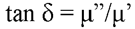
- In the formula, µ' represents the real part of the complex magnetic permeability, and µ" represents the imaginary part of the complex magnetic permeability.
- Examples of the magnetic material contained in the magnetic
wave absorption layer 5 include metals or compounds containing at least one element selected from iron, nickel and cobalt. - The designed
magnetic wave suppressor magnetic wave suppressor design layer 1, so that the designedmagnetic wave suppressor - Building materials formed of the designed
magnetic wave suppressor - The embodiments of the present disclosure have been described so far; however, the present invention should not be construed as being limited to the above embodiments. For example, a mode including the
resistance layer 2 for performing impedance matching has been exemplified as the designedelectromagnetic wave suppressor 10; however, theresistance layer 2 does not have to be provided if no impedance matching is required to be performed. A designedelectromagnetic wave suppressor 30 shown inFig. 5 has a laminated structure including adesign layer 1, an electromagneticwave suppression layer 3, and areflective layer 4 in this order. - The above embodiments have exemplified the designed
electromagnetic wave suppressor reflective layer 4. A non-layered absorber may be used instead of the electromagneticwave absorption layer 5. - The above embodiments have exemplified the designed
electromagnetic wave suppressor design layer 1 on the outermost surface; however, as shown inFigs. 6(a) to 6(c) , a surfaceprotective layer 8 covering thedesign layer 1 may be further provided. The surfaceprotective layer 8 imparts stain resistance, abrasion resistance, or water resistance to the surface of the designed electromagnetic wave suppressor. From the perspective of abrasion resistance and solvent resistance, the resin forming the surfaceprotective layer 8 is preferred to be a urethane resin, and from the perspective of improving surface hardness, it is more preferred to be a urethane resin with isocyanate added to acrylic polyol. - The surface
protective layer 8 may be a layer that imparts antiviral or antibacterial properties to the surface of the designed electromagnetic wave suppressor. In other words, the surfaceprotective layer 8 may contain a binder resin (e.g., the above urethane resins), and an antiviral agent and/or antibacterial agent. The total mass of the antiviral and antibacterial agents in the surfaceprotective layer 8 is preferred to be, for example, 0.2 to 20 parts by mass, more preferred to be 0.2 to 10 parts by mass, and even more preferred to be 3 to 7 parts by mass, with respect to 100 parts by mass of the binder resin. If the surfaceprotective layer 8 contains an antiviral agent and/or antibacterial agent, the design layer is prevented from being deteriorated by, for example, the growth of microbes even when dirt such as oil has adhered to the outermost surface of the designed electromagnetic wave suppressor, so that the electromagnetic wave suppression performance can be maintained for a long period of time. Thedesign layer 1 may be imparted with antiviral and/or antibacterial properties by adding an antiviral agent and/or antibacterial agent to thedesign layer 1. The total mass of the antiviral and antibacterial agents in thedesign layer 1 is preferred to be, for example, 0.2 to 20 parts by mass, more preferred to be 0.2 to 10 parts by mass, and even more preferred to be 3 to 7 parts by mass, with respect to 100 parts by mass of thedesign layer 1. - Imparting antiviral properties refers to that 2 log10 or more antiviral activity is indicated in the antiviral test according to ISO 21702. The antiviral agent refers to a substance having the above antiviral properties. Examples of the antiviral agent that can be used include inorganic antibacterial agents such as antibacterial zeolite, antibacterial apatite, and antibacterial zirconia formed by incorporating metal ions such as silver ions, copper ions, and zinc ions into substances such as zeolite, apatite, zirconia, etc., that are inorganic compounds. Examples of the antiviral agent may include organic antibacterial agents such as zinc pyridine, 2-(4-thiazolyl)-benzimidazole, 10,10-oxybisphenoxazine, organic nitrogen sulfur halogen-based substances, and pyridine-2-thiol-oxide. The antibacterial agent includes silver-based antibacterial agents, inorganic antibacterial agents, organic antibacterial agents, etc., and may be selected according to usage.
- The thickness of the surface
protective layer 8 is preferred to be, for example, 10 µm to 50 µm, more preferred to be 10 µm to 40 µm, and even more preferred to be 10 µm to 25 µm. If the thickness is 10 µm or more, a uniform layer can be easily formed by coating, while securing sufficient surface strength, and there is a tendency that functions as a surfaceprotective layer 8 can be sufficiently achieved. On the other hand, if the thickness is 50 µm or less, there is a tendency that sufficient flexibility can be maintained. - The real part of the complex permittivity of the surface
protective layer 8 is preferred to be 7 or less, more preferred to be 2.0 to 5.0, and even more preferred to be 2.0 to 3.0, from the perspective of suppressing variation in reflection attenuation frequency with respect to the variation in thickness of the surfaceprotective layer 8. The imaginary part of the complex permittivity of the surfaceprotective layer 8 is preferred to be 0.5 or less, more preferred to be 0 to 0.3, and even more preferred to be 0 to 0.1, from the perspective of achieving the return attenuation suitable for practical use. If the real part and/or imaginary part of the complex permittivity of the surfaceprotective layer 8 are in the above ranges, the influence of the surfaceprotective layer 8 on the return attenuation of the electromagnetic wave suppressor can be reduced even when the surfaceprotective layer 8 has a thickness of, for example 50 µm. - Examples and comparative examples of the present disclosure will be described. The present invention should not be construed as being limited to the following examples.
- Electromagnetic wave suppressors related to examples and comparative examples were prepared using the following materials. The real part of the complex permittivity (relative permittivity) and dielectric tangent of the design layer (interior decorative sheet) or the electromagnetic wave suppression layer were measured using Model No. u (manufactured by KEYCOM Corporation). The value of the imaginary part of the complex permittivity was calculated from these measured values.
- Interior decorative sheet: 101 ECO SHEET (manufactured by Toppan Inc., thickness: 140 µm, real part of complex permittivity: 2.85, imaginary part of complex permittivity: 0)
- Mixture (PEDOT/PSS) of polyethylenedioxythiophene (PEDOT) and polystyrene sulfonate (PSS) (manufactured by Nagase ChemteX Corporation).
-
- Magnetic material: Epsilon nano-iron oxide particles (manufactured by Iwatani Corporation)
- Binder resin: Butadiene resin (manufactured by Asahi Kasei Corporation)
- Acrylic adhesive: OC-3405 (trade name, manufactured by Saiden Chemical Industry Co.,Ltd.)
- Nanoparticles of barium titanate (manufactured by Sakai Chemical Industry Co., Ltd., average particle size: 100 nm)
- Al deposited PET film
- A transmissive type electromagnetic wave suppressor whose layers were formed of the materials shown in Table 1 was prepared as follows. Specifically, an electromagnetic wave suppression layer (thickness: 2.5 × 103 µm) was formed using a coating liquid containing 30 parts by mass of binder resin with respect to 100 parts by mass of magnetic material. The real part of the complex permittivity of the electromagnetic wave suppression layer was 0.8 and the imaginary part of the complex permittivity thereof was 0.3. An interior decorative sheet as a design layer was bonded to the surface of the electromagnetic wave suppression layer.
- A reflective type electromagnetic wave suppressor whose layers were formed of the materials shown in Table 1 was prepared as follows. Specifically, an electromagnetic wave suppression layer (thickness: 1,990 µm) was formed using a coating liquid containing 70 parts by mass of acrylic adhesive with respect to 100 parts by mass of barium titanate (BaTiO4). The real part of the complex permittivity of the electromagnetic wave suppression layer was 10.8 and the imaginary part of the complex permittivity thereof was 0.74. An interior decorative sheet as a design layer was bonded to the surface of the electromagnetic wave suppression layer. A reflective layer was provided to the surface of the electromagnetic wave suppression layer facing away from the surface provided with the design layer.
- A reflective type electromagnetic wave suppressor whose layers were formed of the materials shown in Table 1 was prepared as follows. Specifically, an electromagnetic wave suppression layer (thickness: 260 µm) was formed using a coating liquid containing 70 parts by mass of acrylic adhesive with respect to 100 parts by mass of barium titanate (BaTiO4). The real part of the complex permittivity of the electromagnetic wave suppression layer was 10.8 and the imaginary part of the complex permittivity thereof was 0.74. A resistance layer containing PEDOT/PSS (sheet resistance: 430 Ω/sq) was provided to the surface of the electromagnetic wave suppression layer. An interior decorative sheet as a design layer was bonded to the surface of the resistance layer. A reflective layer was provided to the surface of the electromagnetic wave suppression layer facing away from the surface provided with the resistance layer. The sheet resistance of the resistance layer was measured using a high-resistance low-efficiency meter (manufactured by Mitsubishi Chemical Analytic Tech Corporation).
- For comparison with the examples, an Al deposited PET film (reflective layer) that was the same as those used in Examples 1 and 2 was prepared.
- A sample for comparison was prepared as in Example 1 except that no design layer was provided.
- For comparison, a millimeter radio wave absorber with multiple square pyramids arranged side by side (manufactured by Iwatani Corporation) was prepared.
- The effect of suppressing electromagnetic waves was evaluated for the examples and the comparative examples using a free space type S-parameter measurement method. Measurements were performed using the following devices.
Vector network analyzer (Keysight PNA N5222B 10 MHz - 26.5 GHz, manufactured by Virginia Diodes Inc., WR12 55 - 95 GHz)
High frequency network analyzer (E8362C manufactured by Agilent Technologies Inc.) - Millimeter waves were applied to each sample from a transmission antenna, and the intensity of the millimeter waves reflected by the sample and incident on a reception antenna was measured to calculate a return attenuation (dB). The maximum value of the return attenuation in the range of 60 GHz to 90 GHz, and the frequency achieving this maximum value were listed on Tables 1 and 2.
[Table 1] Ex. 1 Ex. 2 Ex. 3 Structure Designed layer Complex permittivity Real part 2.85 2.85 2.85 Imaginary part 0 0 0 Resistance layer Material - - PEDOT/PSS Sheet resistance [Ω/sq] - - 430 Electromagnetic wave suppression layer Material Magnetic material Acrylic adhesive / Ba2TiO4 nano particles Acrylic adhesive / Ba2TiO4 nano particles Complex magnetic permeability / complex permittivity/ 0.8-0.3j 10.8-0.74j 10.8-0.74j Thickness [µm] 2.5×10³ 1990 260 Reflective layer Material - Al/PET Al/PET Evaluation Maximum value of return attenuation [dB] 30 20 40 Frequency [GHz] 76.0 79.0 79.0 [Table 2] Comp. Ex. 1 Comp. Ex. 2 Comp. Ex. 3 Structure Designed layer Permittivity - - - Complex permittivity Real part - - - Imaginary part - - - Resistance layer Material - - - Sheet resistance [Ω/sq] - - - Electromagnetic wave suppression layer Material - Magnetic material Urethane Complex magnetic permeability / complex permittivity/ - 0.8-0.3j - Thickness [µm] - 2.5×10³ 83×103 (Top-bottom distance) Reflective layer Material Al/PET - - Evaluation Maximum value of return attenuation [dB] 0 30 50 Frequency [GHz] - 76.0 76.0 - A reflective type electromagnetic wave suppressor was prepared as in Example 3 except that a surface protective layer having a thickness of 10 µm was provided by coating so as to cover the design layer. Composition of the surface protective layer was as shown below.
- Acrylic resin: ATC-354 (manufactured by DIC Corporation) 100 parts by mass
- Antibacterial agent A: Apacider AW (manufactured by Sangi Co., Ltd., antibacterial material in which metallic silver (silver component) was supported on calcium phosphate)
- 2 parts by mass
- A reflective type electromagnetic wave suppressor was prepared as in Example 3 except that a surface protective layer having a thickness of 10 µm was provided by coating so as to cover the design layer. Composition of the surface protective layer was as shown below.
- Urethan resin: URV283 gloss varnish (manufactured by Toyo Ink Co., Ltd.) 100 parts by mass
- Curing agent: UR150B varnish (manufactured by Toyo Ink Co., Ltd.) 10 parts by mass
- Antibacterial agent B: RASAP QB-2500G (manufactured by RASA Industries, Ltd., inorganic-organic hybrid antibacterial agent in which an organic antibacterial agent was intercalated with a sparingly soluble phosphate) 2 parts by mass
- Table 3 shows evaluations for Examples 3 to 5. In the table, the "initial maximum value of return attenuation" and the "initial frequency" are values measured similarly to the above. These values indicated in "after contamination" are values measured after immersing each sample in ammonium water (10% concentration) for 24 hours and contaminating the design layer (Example 3) or the surface protective layer (Examples 4 and 5) according to JIS K6902:2007.
[Table 3] Ex. 3 Ex. 4 Ex. 5 Structure Surface protective layer - Containing antibacterial agent A Containing antibacterial agent B Designed layer Complex permittivity Real part 2.85 2.85 2.85 Imaginary part 0 0 0 Resistance layer Material PEDOT/PSS PEDOT/PSS PEDOT/PSS Sheet resistance [Ω/sq] 430 430 430 Electromagnetic wave suppression layer Material Acrylic adhesive / Ba2TiO4 nano particles Acrylic adhesive / Ba2TiO4 nano particles Acrylic adhesive / Ba2TiO4 nano particles Complex magnetic permeability / complex permittivity/ 10.8-0.74j 10.8-0.74j 10.8-0.74j Thickness [µm] 260 260 260 Reflective layer Material Al/PET Al/PET Al/PET Evaluation Initial Maximum value of return attenuation [dB] 40 84 46 Frequency [GHz] 79.0 79.0 79.0 After contamination Maximum value of return attenuation [dB] 26 84 46 Frequency [GHz] 72.7 79.0 79.0 -
- 1 ... Design layer
- 2 ... Resistance layer
- 3 ... Electromagnetic wave suppression layer (electromagnetic wave suppressor)
- 4 ... Reflective layer
- 4a ... Surface
- 8 ... Surface protective layer
- 10, 20, 30 ... Designed electromagnetic wave suppressor
Claims (14)
- A designed electromagnetic wave suppressor comprisinga design layer; andan electromagnetic wave suppressor having an electromagnetic wave return attenuation of 10 dB or more.
- The designed electromagnetic wave suppressor according to claim 1, wherein a real part of a complex permittivity of the design layer is 5 or less.
- The designed electromagnetic wave suppressor according to claim 1 or 2, wherein an imaginary part of a complex permittivity of the design layer is 0.5 or less.
- The designed electromagnetic wave suppressor according to any one of claims 1 to 3, wherein the electromagnetic wave suppressor is a laminate including either of a dielectric layer and a magnetic layer, and a reflective layer.
- The designed electromagnetic wave suppressor according to any one of claims 1 to 3, wherein the electromagnetic wave suppressor is a laminate including a resistance layer, either of a dielectric layer and a magnetic layer, and a reflective layer in this order.
- The designed electromagnetic wave suppressor according to claim 5, wherein the resistance layer has a sheet resistance of 270 S2/sq to 500Q/sq .
- The designed electromagnetic wave suppressor according to any one of claims 1 to 6, further comprising a surface protective layer on an outermost surface, the surface protective layer containing at least one of an antiviral agent and an antibacterial agent.
- The designed electromagnetic wave suppressor according to claim 7, wherein the surface protective layer has a thickness of 10 µm to 50 µm.
- The designed electromagnetic wave suppressor according to claim 7 or 8, wherein a real part of a complex permittivity of the surface protective layer is 7 or less.
- The designed electromagnetic wave suppressor according to any one of claims 7 to 9, wherein the antiviral agent contains a silver component.
- The designed electromagnetic wave suppressor according to any one of claims 7 to 10, wherein the antibacterial agent is at least one selected from a group consisting of silver-based antibacterial agents, inorganic antibacterial agents, and organic antibacterial agents.
- A building material comprising the designed electromagnetic wave suppressor according to any one of claims 1 to 11.
- An electromagnetic wave suppression chamber comprisinga room in which at least part of inner walls is covered with the building material according to claim 12; anda transmitter disposed in the room.
- A system comprisingthe electromagnetic wave suppression chamber according to claim 13; anda wireless communication device disposed in the electromagnetic wave suppression chamber.
Applications Claiming Priority (2)
| Application Number | Priority Date | Filing Date | Title |
|---|---|---|---|
| JP2020193306 | 2020-11-20 | ||
| PCT/JP2021/042204 WO2022107797A1 (en) | 2020-11-20 | 2021-11-17 | Designed electromagnetic wave suppressor, construction material equipped with same, electromagnetic wave suppression chamber, and system |
Publications (2)
| Publication Number | Publication Date |
|---|---|
| EP4250891A1 true EP4250891A1 (en) | 2023-09-27 |
| EP4250891A4 EP4250891A4 (en) | 2024-05-29 |
Family
ID=81708019
Family Applications (1)
| Application Number | Title | Priority Date | Filing Date |
|---|---|---|---|
| EP21894671.3A Pending EP4250891A4 (en) | 2020-11-20 | 2021-11-17 | ELECTROMAGNETIC WAVE SUPPRESSOR, CONSTRUCTION MATERIAL EQUIPPED THEREWITH, ELECTROMAGNETIC WAVE SUPPRESSION CHAMBER AND SYSTEM |
Country Status (7)
| Country | Link |
|---|---|
| US (1) | US20240040758A1 (en) |
| EP (1) | EP4250891A4 (en) |
| JP (1) | JPWO2022107797A1 (en) |
| KR (1) | KR20230109698A (en) |
| CN (1) | CN116457197A (en) |
| TW (1) | TW202241249A (en) |
| WO (1) | WO2022107797A1 (en) |
Families Citing this family (3)
| Publication number | Priority date | Publication date | Assignee | Title |
|---|---|---|---|---|
| WO2022125360A1 (en) * | 2020-12-11 | 2022-06-16 | Dow Global Technologies Llc | Preparation of a sound dampened flooring with improved acoustic performance and sound dampened flooring |
| CN114108857B (en) * | 2021-11-22 | 2023-03-28 | 广州新莱福新材料股份有限公司 | Electromagnetic shielding module, electromagnetic shielding structure and construction method of electromagnetic shielding structure |
| WO2023243485A1 (en) * | 2022-06-16 | 2023-12-21 | Toppanホールディングス株式会社 | Electromagnetic wave absorber |
Family Cites Families (15)
| Publication number | Priority date | Publication date | Assignee | Title |
|---|---|---|---|---|
| JP4111565B2 (en) * | 1997-02-06 | 2008-07-02 | リンテック株式会社 | EMI shielding sheet |
| CN101032198B (en) * | 2004-09-29 | 2010-05-12 | 新田株式会社 | Electromagnetic wave absorber |
| JP4176082B2 (en) * | 2005-01-20 | 2008-11-05 | 株式会社ウッドワン | Wood interior finishing material with radio wave absorption performance |
| JP2010157696A (en) * | 2008-12-05 | 2010-07-15 | Toray Ind Inc | Radiowave absorber |
| JP2010153542A (en) | 2008-12-25 | 2010-07-08 | Ado Union Kenkyusho:Kk | Electromagnetic wave suppression sheet and method of manufacturing the same |
| JP5138623B2 (en) * | 2009-03-17 | 2013-02-06 | デクセリアルズ株式会社 | Magnetic sheet and manufacturing method thereof |
| JP6795300B2 (en) | 2015-12-17 | 2020-12-02 | 東洋インキScホールディングス株式会社 | Electromagnetic wave suppression sheet and electromagnetic wave suppression adhesive sheet using it, electromagnetic wave suppression resin composition, electromagnetic wave suppression layer |
| JP2017216337A (en) | 2016-05-31 | 2017-12-07 | Jnc株式会社 | Electromagnetic wave suppression coating agent, electromagnetic wave suppression sheet, electromagnetic wave shield component, and electronic apparatus |
| JP6437168B2 (en) * | 2016-12-27 | 2018-12-12 | 関西ペイント株式会社 | Radio wave absorption sheet for millimeter wave band and millimeter wave radio wave absorption method |
| KR102123392B1 (en) * | 2017-04-13 | 2020-06-29 | 헨켈 아이피 앤드 홀딩 게엠베하 | Thermally conductive emi suppression compositions |
| JP6657479B2 (en) * | 2017-10-12 | 2020-03-04 | イビデン株式会社 | Antiviral substrate, antiviral composition, method for producing antiviral substrate, antimicrobial substrate, antimicrobial composition, and method for producing antimicrobial substrate |
| JP2019102665A (en) * | 2017-12-04 | 2019-06-24 | 国立大学法人北海道大学 | Electromagnetic wave absorber |
| JP7123347B2 (en) * | 2018-03-30 | 2022-08-23 | 住化エンバイロメンタルサイエンス株式会社 | Antiviral composition or method for imparting antiviral function |
| CN109705686A (en) * | 2018-12-13 | 2019-05-03 | 南通蛇类治疗研究所 | The multi-functional green inner wall paint of nano silver system |
| CN111902036B (en) * | 2020-08-12 | 2023-09-22 | 宁波磁性材料应用技术创新中心有限公司 | An electromagnetic wave noise suppression sheet and high-frequency electronic equipment |
-
2021
- 2021-11-17 JP JP2022563792A patent/JPWO2022107797A1/ja active Pending
- 2021-11-17 WO PCT/JP2021/042204 patent/WO2022107797A1/en not_active Ceased
- 2021-11-17 CN CN202180077133.7A patent/CN116457197A/en active Pending
- 2021-11-17 KR KR1020237020357A patent/KR20230109698A/en active Pending
- 2021-11-17 EP EP21894671.3A patent/EP4250891A4/en active Pending
- 2021-11-19 TW TW110143119A patent/TW202241249A/en unknown
-
2023
- 2023-05-18 US US18/199,338 patent/US20240040758A1/en active Pending
Also Published As
| Publication number | Publication date |
|---|---|
| KR20230109698A (en) | 2023-07-20 |
| JPWO2022107797A1 (en) | 2022-05-27 |
| EP4250891A4 (en) | 2024-05-29 |
| WO2022107797A1 (en) | 2022-05-27 |
| CN116457197A (en) | 2023-07-18 |
| US20240040758A1 (en) | 2024-02-01 |
| TW202241249A (en) | 2022-10-16 |
Similar Documents
| Publication | Publication Date | Title |
|---|---|---|
| US20240040758A1 (en) | Designed electromagnetic wave suppressor, and building material, electromagnetic wave suppression chamber, and system provided with the suppressor | |
| KR102041426B1 (en) | Electromagnetic wave absorber and molded article with electromagnetic wave absorber | |
| EP2833478A1 (en) | Electromagnetic radiation attenuator | |
| EP2381756A2 (en) | Electromagnetic wave absorber | |
| US11978959B2 (en) | λ/4 type radio wave absorber | |
| JP7554146B2 (en) | Radio wave absorber | |
| EP2246313B1 (en) | Window glass with conductive ceramic fired body | |
| KR100990154B1 (en) | Electron wave shielding material and manufacturing method of the same | |
| US20230356500A1 (en) | Electromagnetic wave absorber and electromagnetic wave absorber-attached molded article | |
| EP3641519A1 (en) | Electromagnetic-wave absorber and molded article provided with electromagnetic-wave absorber | |
| CA2615343A1 (en) | Wireless network shielding system and method | |
| EP2238207B1 (en) | Paint composition | |
| EP3641518A1 (en) | Electromagnetic-wave absorber and molded article provided with electromagnetic-wave absorber | |
| TW202233050A (en) | Electromagnetic wave shielding body | |
| JP7534997B2 (en) | Radio wave absorber | |
| JP2023183509A (en) | electromagnetic wave absorber | |
| JP3209453B2 (en) | Radio wave antireflective body and radio wave antireflection method | |
| JP2023167269A (en) | Electromagnetic wave absorber, manufacturing method thereof, and stable communication space | |
| EP2367234B1 (en) | Paint with metallic microwires, process for integrating metallic microwires in paint and process for applying said paint on metallic surfaces | |
| JP2023182308A (en) | electromagnetic wave absorber | |
| WO2023243485A1 (en) | Electromagnetic wave absorber |
Legal Events
| Date | Code | Title | Description |
|---|---|---|---|
| STAA | Information on the status of an ep patent application or granted ep patent |
Free format text: STATUS: THE INTERNATIONAL PUBLICATION HAS BEEN MADE |
|
| PUAI | Public reference made under article 153(3) epc to a published international application that has entered the european phase |
Free format text: ORIGINAL CODE: 0009012 |
|
| STAA | Information on the status of an ep patent application or granted ep patent |
Free format text: STATUS: REQUEST FOR EXAMINATION WAS MADE |
|
| 17P | Request for examination filed |
Effective date: 20230324 |
|
| AK | Designated contracting states |
Kind code of ref document: A1 Designated state(s): AL AT BE BG CH CY CZ DE DK EE ES FI FR GB GR HR HU IE IS IT LI LT LU LV MC MK MT NL NO PL PT RO RS SE SI SK SM TR |
|
| DAV | Request for validation of the european patent (deleted) | ||
| DAX | Request for extension of the european patent (deleted) | ||
| A4 | Supplementary search report drawn up and despatched |
Effective date: 20240425 |
|
| RIC1 | Information provided on ipc code assigned before grant |
Ipc: B32B 27/28 20060101ALI20240419BHEP Ipc: B32B 27/14 20060101ALI20240419BHEP Ipc: B32B 15/20 20060101ALI20240419BHEP Ipc: B32B 15/16 20060101ALI20240419BHEP Ipc: B32B 9/04 20060101ALI20240419BHEP Ipc: B32B 9/00 20060101ALI20240419BHEP Ipc: B32B 5/30 20060101ALI20240419BHEP Ipc: B32B 5/16 20060101ALI20240419BHEP Ipc: B32B 5/02 20060101ALI20240419BHEP Ipc: B32B 7/025 20190101ALI20240419BHEP Ipc: H05K 9/00 20060101AFI20240419BHEP |