EP4250725B1 - Systems and methods for aligning imaging devices - Google Patents
Systems and methods for aligning imaging devices Download PDFInfo
- Publication number
- EP4250725B1 EP4250725B1 EP23164190.3A EP23164190A EP4250725B1 EP 4250725 B1 EP4250725 B1 EP 4250725B1 EP 23164190 A EP23164190 A EP 23164190A EP 4250725 B1 EP4250725 B1 EP 4250725B1
- Authority
- EP
- European Patent Office
- Prior art keywords
- test
- lens
- fpa
- imaging device
- test elements
- Prior art date
- Legal status (The legal status is an assumption and is not a legal conclusion. Google has not performed a legal analysis and makes no representation as to the accuracy of the status listed.)
- Active
Links
Images


Classifications
-
- H—ELECTRICITY
- H04—ELECTRIC COMMUNICATION TECHNIQUE
- H04N—PICTORIAL COMMUNICATION, e.g. TELEVISION
- H04N17/00—Diagnosis, testing or measuring for television systems or their details
- H04N17/002—Diagnosis, testing or measuring for television systems or their details for television cameras
-
- G—PHYSICS
- G02—OPTICS
- G02B—OPTICAL ELEMENTS, SYSTEMS OR APPARATUS
- G02B7/00—Mountings, adjusting means, or light-tight connections, for optical elements
- G02B7/003—Alignment of optical elements
- G02B7/004—Manual alignment, e.g. micromanipulators
-
- G—PHYSICS
- G01—MEASURING; TESTING
- G01B—MEASURING LENGTH, THICKNESS OR SIMILAR LINEAR DIMENSIONS; MEASURING ANGLES; MEASURING AREAS; MEASURING IRREGULARITIES OF SURFACES OR CONTOURS
- G01B11/00—Measuring arrangements characterised by the use of optical techniques
- G01B11/26—Measuring arrangements characterised by the use of optical techniques for measuring angles or tapers; for testing the alignment of axes
- G01B11/27—Measuring arrangements characterised by the use of optical techniques for measuring angles or tapers; for testing the alignment of axes for testing the alignment of axes
-
- G—PHYSICS
- G01—MEASURING; TESTING
- G01M—TESTING STATIC OR DYNAMIC BALANCE OF MACHINES OR STRUCTURES; TESTING OF STRUCTURES OR APPARATUS, NOT OTHERWISE PROVIDED FOR
- G01M11/00—Testing of optical apparatus; Testing structures by optical methods not otherwise provided for
- G01M11/02—Testing optical properties
- G01M11/0207—Details of measuring devices
-
- G—PHYSICS
- G01—MEASURING; TESTING
- G01M—TESTING STATIC OR DYNAMIC BALANCE OF MACHINES OR STRUCTURES; TESTING OF STRUCTURES OR APPARATUS, NOT OTHERWISE PROVIDED FOR
- G01M11/00—Testing of optical apparatus; Testing structures by optical methods not otherwise provided for
- G01M11/02—Testing optical properties
- G01M11/0221—Testing optical properties by determining the optical axis or position of lenses
-
- G—PHYSICS
- G02—OPTICS
- G02B—OPTICAL ELEMENTS, SYSTEMS OR APPARATUS
- G02B27/00—Optical systems or apparatus not provided for by any of the groups G02B1/00 - G02B26/00, G02B30/00
- G02B27/62—Optical apparatus specially adapted for adjusting optical elements during the assembly of optical systems
-
- H—ELECTRICITY
- H04—ELECTRIC COMMUNICATION TECHNIQUE
- H04N—PICTORIAL COMMUNICATION, e.g. TELEVISION
- H04N23/00—Cameras or camera modules comprising electronic image sensors; Control thereof
- H04N23/50—Constructional details
- H04N23/55—Optical parts specially adapted for electronic image sensors; Mounting thereof
-
- H—ELECTRICITY
- H04—ELECTRIC COMMUNICATION TECHNIQUE
- H04N—PICTORIAL COMMUNICATION, e.g. TELEVISION
- H04N23/00—Cameras or camera modules comprising electronic image sensors; Control thereof
- H04N23/56—Cameras or camera modules comprising electronic image sensors; Control thereof provided with illuminating means
-
- H—ELECTRICITY
- H10—SEMICONDUCTOR DEVICES; ELECTRIC SOLID-STATE DEVICES NOT OTHERWISE PROVIDED FOR
- H10F—INORGANIC SEMICONDUCTOR DEVICES SENSITIVE TO INFRARED RADIATION, LIGHT, ELECTROMAGNETIC RADIATION OF SHORTER WAVELENGTH OR CORPUSCULAR RADIATION
- H10F39/00—Integrated devices, or assemblies of multiple devices, comprising at least one element covered by group H10F30/00, e.g. radiation detectors comprising photodiode arrays
- H10F39/80—Constructional details of image sensors
- H10F39/802—Geometry or disposition of elements in pixels, e.g. address-lines or gate electrodes
- H10F39/8023—Disposition of the elements in pixels, e.g. smaller elements in the centre of the imager compared to larger elements at the periphery
-
- H—ELECTRICITY
- H10—SEMICONDUCTOR DEVICES; ELECTRIC SOLID-STATE DEVICES NOT OTHERWISE PROVIDED FOR
- H10H—INORGANIC LIGHT-EMITTING SEMICONDUCTOR DEVICES HAVING POTENTIAL BARRIERS
- H10H20/00—Individual inorganic light-emitting semiconductor devices having potential barriers, e.g. light-emitting diodes [LED]
- H10H20/80—Constructional details
- H10H20/81—Bodies
- H10H20/822—Materials of the light-emitting regions
- H10H20/824—Materials of the light-emitting regions comprising only Group III-V materials, e.g. GaP
Definitions
- the present disclosure relates to imaging devices, and more particularly to testing the alignment of components of the imaging devices.
- FPA Focal Plane Array
- This typically requires specialized equipment in order to assure consistent mounting of the camera to the alignment test fixture, and then the imaging of a test card or other suitable pattern so that the optics positioning can be adjusted to bring the test image to the required location.
- Multiple individual items (camera, test card, and lens mount) must be well-controlled in order to achieve an accurate, repeatable alignment outcome.
- the outcome may vary due to physical differences (manufacturing tolerances etc.) between the fixtures.
- US 2018/262662 A1 discloses a system for aligning components of an imaging device including a board on which the imaging device is mounted.
- the board includes light emitting devices and light receiving devices to receive reflected light from the light emitting devices which is used to align the components of the imaging device.
- WO 2018/005063 A1 discloses an alignment system configured to sense a state of alignment between a lens and a sensor of an imaging device, the system comprises alignment markers that are self-illuminating and may include a light-emitting diode.
- the present invention provides a system for aligning components of an imaging device as claimed in claim 1.
- the FPA includes imaging pixels defining a pixel area, guard pixels defining a guard pixel area positioned around a perimeter of the pixel area, and test pixels defining a test pixel area positioned around a perimeter of the guard pixel area.
- Each of the at least two test elements can include a cluster of forward biased diodes positioned in the test pixel area.
- Each of the at least two test elements can be configured and adapted to emit alignment reference light through the lens of the imaging device.
- the forward biased diodes of each cluster can be arranged in at least one of a square shape, a round shape, a diamond shape, and/or an "L" shape.
- the at least two test elements can include four test elements.
- the FPA can define a rectangular imaging area.
- the rectangular imaging area can be a square imaging area.
- the at least two test elements can be positioned proximate to respective corners of the rectangular imaging area.
- the at least two test elements can be positioned at respective mid-points of respective sides of the rectangular imaging
- Each test element can include a cluster of forward biased InGaAs diodes configured and adapted to emit alignment reference light through the lens of the imaging device.
- the at least two test elements can be configured and adapted to emit light in a wavelength ranging from 1650-1700 nm.
- the at least two additional test elements can be configured and adapted to emit light in a wavelength ranging from 1650-1700 nm, 100 - 400 nm, and/or 380 - 700 nm.
- Each cluster of forward biased diodes are configured and adapted to emit alignment reference light through the lens of the imaging device.
- the test elements can be forward biased InGaAs diodes configured and adapted to emit alignment reference light through the lens of the imaging device.
- the present invention also provides a method of testing and aligning a lens of an imaging device as claimed in claim 10.
- the method can include mounting the test camera to the lens of the imaging device so that a test camera FPA is rotated ninety degrees relative to the FPA of the imaging device.
- the method can include mounting the test camera to the lens of the imaging device so that a test camera FPA is rotated forty five degrees relative to the FPA of the imaging device.
- Adjusting the lens of the imaging device can include at least one of moving the lens along a horizontal and/or a vertical axis, and/or rotation about the FPA.
- the method can include focusing the lens of the imaging device to infinity such that the light emitted from the at least two test elements will be collimated and rays emerging from the lens will be parallel to the optical axis.
- the method can include focusing a test camera lens to the at least two test elements.
- Fig. 1 a schematic view of an exemplary embodiment of the system for aligning components of an imaging device in accordance with the disclosure is shown in Fig. 1 and is designated generally by reference character 100.
- the systems and methods described herein can be used to simplify the testing process for imaging devices by using test features on the FPA of the imaging device itself as the source of the test image, instead of a traditional test card. This eliminates the test card and its associated alignment process.
- a system 100 for aligning components of an imaging device 102 includes imaging device 102, and a test camera 104.
- Imaging device 102 includes a lens 106 and a focal plane array (FPA) 108.
- FPA 108 defines an optical axis A and four test elements 112a-112d configured and adapted to emit a light through lens 106.
- the wavelength of the emission from test elements 112a-112d is at an upper end of the SWIR (shortwave infrared) spectrum, ranging from about 1650 - 1700 nm.
- Test elements 112a-112d can be forward biased InGaAs diodes.
- Test camera 104 is configured and adapted to be mounted to and pre-aligned with lens 106 of imaging device 102 to receive a light from test elements 112a-112d.
- Test camera 104 includes a test camera lens 105. Because test camera 104 mounts directly to lens 106, the position of test camera 104 is not independent (as the test card was) and therefore it is, in essence, pre-aligned. This pre-alignment results in a more accurate alignment of lens 106, a simpler set up and faster alignment process, all of which result in reduced cost due to reduced labor hours needed to align lens 106 with the optical axis A.
- a variety of mechanical attachment devices can be used, for example existing alignment test fixtures.
- a threaded adaptor 111 is configured and adapted to thread into threads 113 on lens 106 and threads 115 of test camera lens 105, thereby attaching the test camera 104 to imaging device 102.
- lens 106 is of custom design, said design may incorporate suitable mounting or alignment details (threaded adapters similar to above, pegs/locating holes, mechanical guides etc.) which will serve to affix the test camera 104 to lens 106.
- Test camera 104 will respond to the light emitted by test elements 112a-112d, and their relative positions can therefore be determined by test camera 104.
- Lens 106 alignment is achieved by adjusting the position of lens 106 until the detected positions of the test features 112a-112d matches the desired (pre-calculated) positions expected to be seen by test camera 104.
- Embodiments of the present disclosure can be used to eliminate offsets in both the horizontal axis X (schematically shown to be extending in and out of the page in Fig. 1 ) direction and the vertical axis Y direction (shown perpendicular to horizontal axis X), as well as rotation about the FPA optical axis A.
- FPA 108 is positioned on a printed circuit board assembly (PCBA) 114 of imaging device 102.
- Test elements 112a-112d are electrically coupled to control circuitry 132 positioned on the PCBA 114 to drive the light emission.
- Control circuitry 132 can be positioned in a variety of suitable places, such as off-chip, meaning it does not need to be incorporated into the PCBA or readout integrated circuit (ROIC).
- These test elements 112a-112d are positioned within FPA diode arrays 116.
- These FPA diode arrays 116 typically surround a rectangular imaging area 118, where rectangular includes a square shape.
- Diode arrays 116 around the imaging area 118 are generally used to test for dark current and other parameters to ensure FPA 108 meets specifications. In testing for dark current and/or other parameters (and in normal operation of the imaging area 118 of the array), the diodes of diode array 116 of the present disclosure are reverse biased. In embodiments of the present disclosure, test elements 112a-112d are forward biased diodes such that they will emit light in the same manner as a standard light-emitting diode (LED).
- LED standard light-emitting diode
- the imaging area 118 of FPA 108 includes imaging pixels 110 defining a pixel area 120, and guard pixels 122 defining a guard pixel area 124 positioned around a perimeter of the pixel area 120.
- Guard pixels 122 are contiguous with the imaging pixels 110 and extend out for several rows and columns along each edge. Guard pixels 122 act to mitigate any 'edge effects' that might occur at the periphery of pixel area 120.
- Test diode array 116 includes test diodes 126 positioned around a perimeter of guard pixel area 124. Test diodes 126 are located just beyond guard pixels 122 and act to check dark current, as described above.
- Each test element 112a-112d includes a cluster of forward biased diodes 128 (which are test diodes 126 in a forward biased position) positioned in the test diode array 116 (test element 112b is shown in Fig. 2B and test elements 112a, 112c and 112d are all similar).
- test diodes 126 are fabricated from InGaAs and when forward biased, like forward biased diodes 128, they will emit SWIR light in the same manner of a standard LED.
- test elements 112a-112d may be used for to make up suitable test elements 112a-112d and that a variety of wavelengths can be emitted. It is contemplated that light with other wavelengths in the electromagnetic spectrum can also be emitted by test elements 112a-112d, such as, visible light (380-700 nm), UltraViolet light (100-400nm), and the like. Those skilled in the art will readily appreciate that as long as test diodes 126 are capable of emitting light when they are forward biased, they will provide suitable diodes to make up test elements 112a-112d.
- Forward biased diodes 128 are configured and adapted to emit alignment reference light through lens 106 of imaging device 102.
- Forward biased diodes 128 of test element 112b are shown arranged in a diamond shape, but those skilled in the art will readily appreciate that a variety of suitable shapes may be used, such as a square shape, a round shape, and/or an "L" shape.
- test elements 112a-112d may be needed to provide proper alignment, e.g. test elements 112a and 112b.
- Two test elements 112b and 112c are positioned adjacent to opposite corners of FPA 108.
- only two of test elements 112a-112d may be needed to provide proper alignment of lens 106.
- the two elements used could be test elements 112a and 112c, or 112a and 112d.
- the test camera 104 is set up so that a test camera FPA 130, shown in Fig. 1 , is rotated 90° from FPA 108.
- test elements 112a-112d are test elements 112a-112d to fall within an imaging area of FPA 130 of test camera 104 so that the position of the test elements 112a-112d can be determined.
- test elements 112a-112d should be close to the edges of FPA 108 so they can be as far apart as possible (while still falling within the detecting area of FPA 130 of test camera 104. Having test elements 112a-112d as far apart as possible, while still falling within the detecting area of FPA 130, provides for the best possible accuracy in measurement, as any measurement error will result in smallest angular distortion.
- FPA 208 is the same as FPA 108 except that FPA 208 has a square shape where two test elements 212 are positioned at the midpoints of respective edges, instead of being toward the corners of FPA 208.
- FPA 208 includes an imaging area 218, similar to imaging area 118. Imaging area 218 defines a pixel area 220 and a guard pixel area 224, which are the same as pixel area 120 and guard pixel area 124, except for the square shape.
- Test elements 212 are positioned within a test diode array 216.
- Test diode array 216 is the same as test diode array 116, except that the four edges of test diode array 216 are the same length and test elements 212 are positioned at the mid-points of respective edges.
- Each test element 212 includes a cluster of forward biased diodes and is positioned in the test diode array 216.
- a square test camera FPA 230 can be rotated 45 degrees relative to the edges of FPA 208 or a rectangle test camera FPA 130 can be rotated 45 degrees relative to the edges of FPA 208 and the test elements 212 will fall within the imaging area of the test camera defined by the test camera FPA 230.
- Test camera FPA 230 can be used in test camera 204.
- test camera should be rotated.
- test camera should be rotated.
- a method of testing and aligning a lens, e.g., lens 106, of an imaging device, e.g., imaging device 102 includes mounting a test camera, e.g. the test camera 104, to the lens of the imaging device so that a test camera FPA, e.g. FPA 130, is rotated ninety degrees relative to an FPA, e.g. FPA 108, of the imaging device.
- Mounting the test camera to the lens of the imaging device includes mounting a first side of a threaded adaptor, e.g. threaded adaptor 111, to the lens of the imaging device and then mounting the test camera lens to a second side of the threaded adaptor.
- mounting the test camera to the lens of the imaging device includes mounting the test camera such that a test camera FPA, e.g. test camera FPA 130, is rotated at 45 degrees relative to the square FPA.
- the method includes emitting light with at least two test elements, e.g., test elements 112a-112d, or 212, positioned within a diode array, e.g. diode array 116 or 216, of the FPA of the imaging device.
- the FPA defines an optical axis, e.g., optical axis A.
- the method includes focusing the lens of the imaging device to infinity such that the light emitted from the test elements will be collimated and rays emerging from the lens will be parallel to the optical axis.
- the method includes focusing a test camera lens, e.g., test camera lens 105, to the test elements. The focus of the lens should be adjusted for sharpest detail on the test elements.
- the method includes detecting the light with the test camera mounted to the lens of the imaging device to determine if the light emitted is in a desired position. To determine this, the test camera will respond to the light emitted by the test elements (e.g. the SWIR light), and their relative positions can therefore be determined.
- the test camera will respond to the light emitted by the test elements (e.g. the SWIR light), and their relative positions can therefore be determined.
- the method includes adjusting the lens of the imaging device until the light emitted by these test features is detected by the test camera in the desired position.
- the lens alignment is achieved by adjusting the position of the lens until the detected positions of the test elements matches the desired (pre-calculated) positions.
- Adjusting the lens of the imaging device includes moving the lens along a horizontal and/or a vertical axis, e.g., horizontal axis X and vertical axis Y, and/or rotation about the FPA about optical axis A. This method can be used to eliminate offsets in both horizontal and vertical axes, as well as rotation about the optical axis.
- Embodiments of the present disclosure include manufacturing and/or retrofitting a Readout Integrated Circuit (ROIC) or Photodiode Array (PDA) to include metallization to allow the test elements to be operated in LED mode.
- ROIC Readout Integrated Circuit
- PDA Photodiode Array
- Embodiments of system 100 provide for more accurate alignment as compared with the traditional test card approach, simpler set-up, and quicker test procedures.
- the faster set-up and quicker test procedure results in reduced labor hours and costs savings.
- the simpler set up stems from not having to align a test card with the FPA optical axis A. Instead, the test camera 104 and lens 105 attach directly to the lens 106 to be aligned.
- the faster alignment process results from the four, widely-separated test elements as the references, misalignment is magnified to the greatest extent possible, and the operator can see the effects of the alignment adjustment in real time.
Landscapes
- Physics & Mathematics (AREA)
- General Physics & Mathematics (AREA)
- Engineering & Computer Science (AREA)
- Optics & Photonics (AREA)
- Multimedia (AREA)
- Signal Processing (AREA)
- Analytical Chemistry (AREA)
- Chemical & Material Sciences (AREA)
- General Health & Medical Sciences (AREA)
- Biomedical Technology (AREA)
- Health & Medical Sciences (AREA)
- Studio Devices (AREA)
- Cameras In General (AREA)
Description
- The present disclosure relates to imaging devices, and more particularly to testing the alignment of components of the imaging devices.
- In many camera applications, it is necessary to align the optical elements of the system lens with the center of the active area of the Focal Plane Array (FPA), also known as the optical axis. This typically requires specialized equipment in order to assure consistent mounting of the camera to the alignment test fixture, and then the imaging of a test card or other suitable pattern so that the optics positioning can be adjusted to bring the test image to the required location. Multiple individual items (camera, test card, and lens mount) must be well-controlled in order to achieve an accurate, repeatable alignment outcome. In addition, if different test fixtures are used, the outcome may vary due to physical differences (manufacturing tolerances etc.) between the fixtures.
-
US 2018/262662 A1 discloses a system for aligning components of an imaging device including a board on which the imaging device is mounted. The board includes light emitting devices and light receiving devices to receive reflected light from the light emitting devices which is used to align the components of the imaging device. -
WO 2018/005063 A1 discloses an alignment system configured to sense a state of alignment between a lens and a sensor of an imaging device, the system comprises alignment markers that are self-illuminating and may include a light-emitting diode. - The conventional techniques have been considered satisfactory for their intended purpose. However, there is a need for improved systems and methods for aligning components of an imaging device. This disclosure provides a solution for this need.
- The present invention provides a system for aligning components of an imaging device as claimed in claim 1.
- In accordance with some embodiments, the FPA includes imaging pixels defining a pixel area, guard pixels defining a guard pixel area positioned around a perimeter of the pixel area, and test pixels defining a test pixel area positioned around a perimeter of the guard pixel area. Each of the at least two test elements can include a cluster of forward biased diodes positioned in the test pixel area. Each of the at least two test elements can be configured and adapted to emit alignment reference light through the lens of the imaging device. The forward biased diodes of each cluster can be arranged in at least one of a square shape, a round shape, a diamond shape, and/or an "L" shape. The at least two test elements can include four test elements. The FPA can define a rectangular imaging area. The rectangular imaging area can be a square imaging area. The at least two test elements can be positioned proximate to respective corners of the rectangular imaging area. The at least two test elements can be positioned at respective mid-points of respective sides of the rectangular imaging area.
- Two test elements can define an axis. Each test element can include a cluster of forward biased InGaAs diodes configured and adapted to emit alignment reference light through the lens of the imaging device. The at least two test elements can be configured and adapted to emit light in a wavelength ranging from 1650-1700 nm. The at least two additional test elements can be configured and adapted to emit light in a wavelength ranging from 1650-1700 nm, 100 - 400 nm, and/or 380 - 700 nm. Each cluster of forward biased diodes are configured and adapted to emit alignment reference light through the lens of the imaging device. The test elements can be forward biased InGaAs diodes configured and adapted to emit alignment reference light through the lens of the imaging device.
- The present invention also provides a method of testing and aligning a lens of an imaging device as claimed in claim 10.
- The method can include mounting the test camera to the lens of the imaging device so that a test camera FPA is rotated ninety degrees relative to the FPA of the imaging device. The method can include mounting the test camera to the lens of the imaging device so that a test camera FPA is rotated forty five degrees relative to the FPA of the imaging device. Adjusting the lens of the imaging device can include at least one of moving the lens along a horizontal and/or a vertical axis, and/or rotation about the FPA. The method can include focusing the lens of the imaging device to infinity such that the light emitted from the at least two test elements will be collimated and rays emerging from the lens will be parallel to the optical axis. The method can include focusing a test camera lens to the at least two test elements.
- These and other features of the systems and methods of the subject disclosure will become more readily apparent to those skilled in the art from the following detailed description of the preferred embodiments taken in conjunction with the drawings.
- So that those skilled in the art to which the subject disclosure appertains will readily understand how to make and use the devices and methods of the subject disclosure without undue experimentation, preferred embodiments thereof will be described in detail herein below with reference to certain figures, wherein:
-
Fig. 1 is a schematic view of a system for aligning components of an imaging device constructed in accordance with an embodiment of the present disclosure, showing an imaging device having an FPA and a lens and a test camera; -
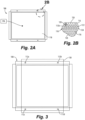
Fig. 2A is a schematic top plan view of the FPA of the imaging device ofFig. 1 , showing four test elements; -
Fig. 2B is an enlarged schematic top plan view of the FPA ofFig. 2B , showing the pixel area and the guard pixel area; -
Fig. 3 is a schematic top plan view of the FPA of the imaging device ofFig. 1 , schematically showing the rotated overlay of the FPA of the test camera; and -
Fig. 4 is a schematic top plan view of another embodiment of an FPA constructed in accordance with an embodiment of the present disclosure, schematically showing the rotated overlay of the FPA of the test camera. - Reference will now be made to the drawings wherein like reference numerals identify similar structural features or aspects of the subject disclosure. For purposes of explanation and illustration, and not limitation, a schematic view of an exemplary embodiment of the system for aligning components of an imaging device in accordance with the disclosure is shown in
Fig. 1 and is designated generally by reference character 100. Other embodiments of the system for aligning components of an imaging device in accordance with the disclosure, or aspects thereof, are provided inFigs. 2A-4 , as will be described. The systems and methods described herein can be used to simplify the testing process for imaging devices by using test features on the FPA of the imaging device itself as the source of the test image, instead of a traditional test card. This eliminates the test card and its associated alignment process. - As shown in
Fig. 1 , a system 100 for aligning components of animaging device 102 includesimaging device 102, and atest camera 104.Imaging device 102 includes alens 106 and a focal plane array (FPA) 108. FPA 108 defines an optical axis A and fourtest elements 112a-112d configured and adapted to emit a light throughlens 106. In the embodiment ofFig. 1 , the wavelength of the emission fromtest elements 112a-112d is at an upper end of the SWIR (shortwave infrared) spectrum, ranging from about 1650 - 1700 nm.Test elements 112a-112d can be forward biased InGaAs diodes.Test camera 104 is configured and adapted to be mounted to and pre-aligned withlens 106 ofimaging device 102 to receive a light fromtest elements 112a-112d.Test camera 104 includes atest camera lens 105. Becausetest camera 104 mounts directly tolens 106, the position oftest camera 104 is not independent (as the test card was) and therefore it is, in essence, pre-aligned. This pre-alignment results in a more accurate alignment oflens 106, a simpler set up and faster alignment process, all of which result in reduced cost due to reduced labor hours needed to alignlens 106 with the optical axis A. - With continued reference to
Fig. 1 , a variety of mechanical attachment devices can be used, for example existing alignment test fixtures. Those skilled in the art will readily appreciate that there are a variety of commercially available lenses equipped with a cylindrical threaded receptacle used to mount filters or other optical elements. In the embodiment ofFig. 1 , a threadedadaptor 111 is configured and adapted to thread intothreads 113 onlens 106 andthreads 115 oftest camera lens 105, thereby attaching thetest camera 104 toimaging device 102. Alternatively, if thelens 106 is of custom design, said design may incorporate suitable mounting or alignment details (threaded adapters similar to above, pegs/locating holes, mechanical guides etc.) which will serve to affix thetest camera 104 tolens 106.Test camera 104 will respond to the light emitted bytest elements 112a-112d, and their relative positions can therefore be determined bytest camera 104.Lens 106 alignment is achieved by adjusting the position oflens 106 until the detected positions of thetest features 112a-112d matches the desired (pre-calculated) positions expected to be seen bytest camera 104. Embodiments of the present disclosure can be used to eliminate offsets in both the horizontal axis X (schematically shown to be extending in and out of the page inFig. 1 ) direction and the vertical axis Y direction (shown perpendicular to horizontal axis X), as well as rotation about the FPA optical axis A. - With continued reference to
Fig. 1 ,FPA 108 is positioned on a printed circuit board assembly (PCBA) 114 ofimaging device 102.Test elements 112a-112d are electrically coupled to controlcircuitry 132 positioned on thePCBA 114 to drive the light emission.Control circuitry 132 can be positioned in a variety of suitable places, such as off-chip, meaning it does not need to be incorporated into the PCBA or readout integrated circuit (ROIC). Thesetest elements 112a-112d are positioned withinFPA diode arrays 116. TheseFPA diode arrays 116 typically surround arectangular imaging area 118, where rectangular includes a square shape.Diode arrays 116 around theimaging area 118 are generally used to test for dark current and other parameters to ensureFPA 108 meets specifications. In testing for dark current and/or other parameters (and in normal operation of theimaging area 118 of the array), the diodes ofdiode array 116 of the present disclosure are reverse biased. In embodiments of the present disclosure,test elements 112a-112d are forward biased diodes such that they will emit light in the same manner as a standard light-emitting diode (LED). - As shown in
Figs. 2A-2B , theimaging area 118 ofFPA 108 includes imagingpixels 110 defining apixel area 120, andguard pixels 122 defining aguard pixel area 124 positioned around a perimeter of thepixel area 120.Guard pixels 122 are contiguous with theimaging pixels 110 and extend out for several rows and columns along each edge.Guard pixels 122 act to mitigate any 'edge effects' that might occur at the periphery ofpixel area 120.Test diode array 116 includestest diodes 126 positioned around a perimeter ofguard pixel area 124.Test diodes 126 are located just beyondguard pixels 122 and act to check dark current, as described above. Eachtest element 112a-112d includes a cluster of forward biased diodes 128 (which aretest diodes 126 in a forward biased position) positioned in the test diode array 116 (test element 112b is shown inFig. 2B andtest elements Figs. 2A-2B ,test diodes 126 are fabricated from InGaAs and when forward biased, like forwardbiased diodes 128, they will emit SWIR light in the same manner of a standard LED. Those skilled in the art will readily appreciate that a variety of light-emitting diodes may be used for to make upsuitable test elements 112a-112d and that a variety of wavelengths can be emitted. It is contemplated that light with other wavelengths in the electromagnetic spectrum can also be emitted bytest elements 112a-112d, such as, visible light (380-700 nm), UltraViolet light (100-400nm), and the like. Those skilled in the art will readily appreciate that as long astest diodes 126 are capable of emitting light when they are forward biased, they will provide suitable diodes to make uptest elements 112a-112d. By forward-biasing already existingtest diodes 126 intest diode array 116, the forwardbiased diodes 128 that make uptest elements 112a-112d are allowed to be fabricated on the detector material as part of the existing processing - so thetest elements 112a-112d incur no additional cost. Forward biaseddiodes 128 are configured and adapted to emit alignment reference light throughlens 106 ofimaging device 102. Forward biaseddiodes 128 oftest element 112b are shown arranged in a diamond shape, but those skilled in the art will readily appreciate that a variety of suitable shapes may be used, such as a square shape, a round shape, and/or an "L" shape. - With reference to
Fig. 3 , it is contemplated that only two oftest elements 112a-112d may be needed to provide proper alignment,e.g. test elements test elements FPA 108. In this way, in some embodiments of the invention, only two oftest elements 112a-112d may be needed to provide proper alignment oflens 106. Those skilled in the art will readily appreciate that the two elements used could betest elements test camera 104 is set up so that atest camera FPA 130, shown inFig. 1 , is rotated 90° fromFPA 108.Fig. 3 schematically shows the area of thetest camera FPA 130 overlaid on theFPA 108. The rotation oftest camera 104 allows fortest elements 112a-112d to fall within an imaging area ofFPA 130 oftest camera 104 so that the position of thetest elements 112a-112d can be determined. In general,test elements 112a-112d should be close to the edges ofFPA 108 so they can be as far apart as possible (while still falling within the detecting area ofFPA 130 oftest camera 104. Havingtest elements 112a-112d as far apart as possible, while still falling within the detecting area ofFPA 130, provides for the best possible accuracy in measurement, as any measurement error will result in smallest angular distortion. - As shown in
Fig. 4 , another embodiment of anFPA 208 for use inimaging device 102 of system 100 is shown.FPA 208 is the same asFPA 108 except thatFPA 208 has a square shape where twotest elements 212 are positioned at the midpoints of respective edges, instead of being toward the corners ofFPA 208.FPA 208 includes animaging area 218, similar toimaging area 118.Imaging area 218 defines apixel area 220 and aguard pixel area 224, which are the same aspixel area 120 andguard pixel area 124, except for the square shape.Test elements 212 are positioned within atest diode array 216.Test diode array 216 is the same astest diode array 116, except that the four edges oftest diode array 216 are the same length and testelements 212 are positioned at the mid-points of respective edges. Eachtest element 212 includes a cluster of forward biased diodes and is positioned in thetest diode array 216. By having eachtest element 212 positioned at the mid-point of a respective edge, a squaretest camera FPA 230 can be rotated 45 degrees relative to the edges ofFPA 208 or a rectangletest camera FPA 130 can be rotated 45 degrees relative to the edges ofFPA 208 and thetest elements 212 will fall within the imaging area of the test camera defined by thetest camera FPA 230.Test camera FPA 230 can be used in test camera 204. Those skilled in the art will readily appreciate that if the original FPA is square, such asFPA 208, and the test camera has a squaretest camera FPA 230, the test camera should be rotated. Those skilled in the art will appreciate that you can use any test camera with a given FPA shape, as long as in the un-aligned state, the test features will be within the imaging area defined by the FPA of the test camera. - In accordance with another aspect, a method of testing and aligning a lens, e.g.,
lens 106, of an imaging device, e.g.,imaging device 102, includes mounting a test camera, e.g. thetest camera 104, to the lens of the imaging device so that a test camera FPA, e.g.FPA 130, is rotated ninety degrees relative to an FPA, e.g.FPA 108, of the imaging device. Mounting the test camera to the lens of the imaging device includes mounting a first side of a threaded adaptor, e.g. threadedadaptor 111, to the lens of the imaging device and then mounting the test camera lens to a second side of the threaded adaptor. Where a square FPA, e.g.square FPA 208, is used, those skilled in the art will readily appreciate that mounting the test camera to the lens of the imaging device includes mounting the test camera such that a test camera FPA, e.g.test camera FPA 130, is rotated at 45 degrees relative to the square FPA. - The method includes emitting light with at least two test elements, e.g.,
test elements 112a-112d, or 212, positioned within a diode array,e.g. diode array test camera lens 105, to the test elements. The focus of the lens should be adjusted for sharpest detail on the test elements. The method includes detecting the light with the test camera mounted to the lens of the imaging device to determine if the light emitted is in a desired position. To determine this, the test camera will respond to the light emitted by the test elements (e.g. the SWIR light), and their relative positions can therefore be determined. - The method includes adjusting the lens of the imaging device until the light emitted by these test features is detected by the test camera in the desired position. The lens alignment is achieved by adjusting the position of the lens until the detected positions of the test elements matches the desired (pre-calculated) positions. Adjusting the lens of the imaging device includes moving the lens along a horizontal and/or a vertical axis, e.g., horizontal axis X and vertical axis Y, and/or rotation about the FPA about optical axis A. This method can be used to eliminate offsets in both horizontal and vertical axes, as well as rotation about the optical axis. Embodiments of the present disclosure include manufacturing and/or retrofitting a Readout Integrated Circuit (ROIC) or Photodiode Array (PDA) to include metallization to allow the test elements to be operated in LED mode.
- Embodiments of system 100 provide for more accurate alignment as compared with the traditional test card approach, simpler set-up, and quicker test procedures. The faster set-up and quicker test procedure results in reduced labor hours and costs savings. The simpler set up stems from not having to align a test card with the FPA optical axis A. Instead, the
test camera 104 andlens 105 attach directly to thelens 106 to be aligned. The faster alignment process results from the four, widely-separated test elements as the references, misalignment is magnified to the greatest extent possible, and the operator can see the effects of the alignment adjustment in real time. - The methods and systems of the present disclosure, as described above and shown in the drawings, provide for systems and methods for aligning components of an imaging device with superior properties including simpler set-up, faster alignment process and lower cost. The systems and methods of the present invention can apply to a variety of imaging devices, or the like. While the apparatus and methods of the subject disclosure have been shown and described with reference to preferred embodiments, those skilled in the art will readily appreciate that changes and/or modifications may be made thereto without departing from the scope of the invention defined in the appended claims.
Claims (15)
- A system (100) for aligning components of an imaging device, the system comprising:an imaging device (102) including a lens (106) and a focal plane array (108), FPA, wherein the FPA defines an optical axis (A) and includes at least two test elements (112a-112d) configured and adapted to emit a light through the lens; and characterized in that the system further comprisesa test camera (104) configured and adapted to be mounted to and pre-aligned with the lens of the imaging device to receive the light from the at least two test elements.
- The system as recited in claim 1, wherein the FPA includes imaging pixels (110) defining a pixel area (120), guard pixels defining a guard pixel area (124) positioned around a perimeter of the pixel area, and test pixels (126) defining a test pixel area positioned around a perimeter of the guard pixel area.
- The system as recited in claim 2, wherein each of the at least two test elements (112a-112d) includes a cluster of forward biased diodes (128) positioned in the test pixel area, wherein each of the at least two test elements is configured and adapted to emit alignment reference light through the lens of the imaging device, optionally
wherein the forward biased diodes of each cluster can be arranged in at least one of a square shape, a round shape, a diamond shape, and/or an "L" shape. - The system as recited in any preceding claim, wherein each test element includes a cluster of forward biased diodes configured and adapted to emit alignment reference light through the lens of the imaging device, optionally wherein the forward biased diodes are InGaAs diodes; or
wherein the at least two test elements are forward biased InGaAs diodes configured and adapted to emit alignment reference light through the lens of the imaging device. - The system as recited in any preceding claim, wherein the at least two test elements are configured and adapted to emit light in a wavelength ranging from 1650 - 1700 nm; and/or wherein the at least two test elements are configured and adapted to emit light in a wavelength ranging from 100 - 400 nm; and/or wherein the at least two test elements are configured and adapted to emit light in a wavelength ranging from 380 - 700 nm.
- The system as recited in any preceding claim, wherein the at least two test elements includes four test elements.
- The system as recited in any preceding claim, wherein the FPA defines a rectangular imaging area (118), and wherein the at least two test elements are positioned proximate to respective corners of the rectangular imaging area.
- The system as recited in any of claims 1-6, wherein the FPA defines a rectangular imaging area (118), and wherein the at least two test elements are positioned at respective mid-points of respective sides of the rectangular imaging area.
- The system as recited in any preceding claim, wherein the FPA defines a square imaging area.
- A method of testing and aligning a lens (106) of an imaging device (102), the method including:emitting light with at least two test elements (112a-112d) positioned within a focal plane array (108), FPA, of the imaging device, wherein the FPA defines an optical axis (A);detecting the light with a test camera (104) mounted to and pre-aligned with the lens of the imaging device to determine if the light emitted is in a desired position; andadjusting the lens of the imaging device until the light emitted by the at least two test elements is detected by the test camera in the desired position.
- The method as recited in claim 10, further comprising mounting the test camera to the lens of the imaging device so that a test camera FPA is rotated ninety degrees relative to the FPA of the imaging device.
- The method as recited in claim 10, further comprising mounting the test camera to the lens of the imaging device so that a test camera FPA is rotated forty five degrees relative to the FPA of the imaging device.
- The method as recited in any of claims 10-12, wherein adjusting the lens of the imaging device includes at least one of moving the lens along a horizontal axis and/or a vertical axis, and/or rotation about the FPA.
- The method as recited in any of claims 10-13, further comprising focusing the lens of the imaging device to infinity such that the light emitted from the at least two test elements will be collimated and rays emerging from the lens will be parallel to the optical axis.
- The method as recited in any of claims 10-14, further comprising focusing a test camera lens to the at least two test elements.
Applications Claiming Priority (1)
| Application Number | Priority Date | Filing Date | Title |
|---|---|---|---|
| US17/704,761 US12339514B2 (en) | 2022-03-25 | 2022-03-25 | Systems and methods for aligning imaging devices |
Publications (2)
| Publication Number | Publication Date |
|---|---|
| EP4250725A1 EP4250725A1 (en) | 2023-09-27 |
| EP4250725B1 true EP4250725B1 (en) | 2025-04-23 |
Family
ID=85772639
Family Applications (1)
| Application Number | Title | Priority Date | Filing Date |
|---|---|---|---|
| EP23164190.3A Active EP4250725B1 (en) | 2022-03-25 | 2023-03-24 | Systems and methods for aligning imaging devices |
Country Status (3)
| Country | Link |
|---|---|
| US (1) | US12339514B2 (en) |
| EP (1) | EP4250725B1 (en) |
| IL (1) | IL301652B2 (en) |
Family Cites Families (10)
| Publication number | Priority date | Publication date | Assignee | Title |
|---|---|---|---|---|
| JP3793365B2 (en) | 1999-04-12 | 2006-07-05 | ペンタックス株式会社 | Camera body |
| US20090225162A1 (en) | 2008-03-06 | 2009-09-10 | Lustrous International Technology Ltd. | Monitoring apparatus |
| US9167161B1 (en) * | 2013-08-30 | 2015-10-20 | Amazon Technologies, Inc. | Camera module package with a folded substrate and laterally positioned components |
| US9210306B1 (en) | 2014-05-31 | 2015-12-08 | Apple Inc. | Method and system for a single frame camera module active alignment tilt correction |
| US9651658B2 (en) | 2015-03-27 | 2017-05-16 | Google Inc. | Methods and systems for LIDAR optics alignment |
| WO2017094078A1 (en) * | 2015-11-30 | 2017-06-08 | 富士通フロンテック株式会社 | Image pickup device and method for manufacturing image pickup device |
| US10542201B2 (en) | 2016-06-29 | 2020-01-21 | Microsoft Technology Licensing, Llc | Split-camera autoalignment |
| US10094916B1 (en) | 2017-06-09 | 2018-10-09 | Waymo Llc | LIDAR optics alignment systems and methods |
| CN112904171A (en) | 2021-01-19 | 2021-06-04 | 中国兵器工业集团第二一四研究所苏州研发中心 | Four-quadrant photoelectric detector test system and test method |
| TWI768923B (en) * | 2021-05-24 | 2022-06-21 | 致伸科技股份有限公司 | Alignment method of camera lens and light source |
-
2022
- 2022-03-25 US US17/704,761 patent/US12339514B2/en active Active
-
2023
- 2023-03-24 EP EP23164190.3A patent/EP4250725B1/en active Active
- 2023-03-26 IL IL301652A patent/IL301652B2/en unknown
Also Published As
| Publication number | Publication date |
|---|---|
| US12339514B2 (en) | 2025-06-24 |
| IL301652B2 (en) | 2026-05-01 |
| EP4250725A1 (en) | 2023-09-27 |
| IL301652A (en) | 2023-10-01 |
| US20230305259A1 (en) | 2023-09-28 |
| IL301652B1 (en) | 2026-01-01 |
Similar Documents
| Publication | Publication Date | Title |
|---|---|---|
| US7646419B2 (en) | Multiband camera system | |
| US10680023B2 (en) | Optoelectronic modules having a silicon substrate, and fabrication methods for such modules | |
| US6870949B2 (en) | Coaxial narrow angle dark field lighting | |
| CN110741278B (en) | LIDAR optical alignment system and method | |
| US8289387B2 (en) | Vision system, method for installing a vision system and method for manufacturing a vision system | |
| KR101841301B1 (en) | Sensor for checking value documents | |
| US8482816B2 (en) | Document acquisition system and document acquisition method | |
| CN110632727B (en) | Optical lens, camera module and assembling method thereof | |
| JP2005534903A (en) | Light source detection and classification system and manufacturing method for automatic vehicle exterior lighting control | |
| US9608142B2 (en) | Optoelectronic modules with optics integrated into a cap | |
| CN100406842C (en) | Position detection device, position detection method, testing device and camera module manufacturing device | |
| KR20050085408A (en) | Instrument for testing solid-state imaging device | |
| KR101897043B1 (en) | Optical inspection apparatus for performing automatic illumination processing and optical inspection method using the apparatus | |
| US7614144B2 (en) | Component mounting apparatus | |
| EP1679637A2 (en) | Targeting system for a portable image reader | |
| EP4250725A1 (en) | Systems and methods for aligning imaging devices | |
| JPH0243511A (en) | Method for aligning image sensor pair with optical system | |
| JP7075831B2 (en) | Light source module and alignment method of light source module | |
| JP2023505567A (en) | Apparatus, method and use of apparatus for adjusting, assembling and/or testing electro-optical systems | |
| EP3405760B1 (en) | Hyperspectral sensor with ambient light detector | |
| CN116896680A (en) | Photoelectric sensor with collimator and method for visualizing field of view | |
| KR20120123538A (en) | Detection method and detection device | |
| US20040239952A1 (en) | Sensor for visual position detection with a modular lighting unit | |
| US20080149853A1 (en) | Light shaping apparatus | |
| CN118275088A (en) | Rear projection type super-lens detection device and detection method |
Legal Events
| Date | Code | Title | Description |
|---|---|---|---|
| PUAI | Public reference made under article 153(3) epc to a published international application that has entered the european phase |
Free format text: ORIGINAL CODE: 0009012 |
|
| STAA | Information on the status of an ep patent application or granted ep patent |
Free format text: STATUS: THE APPLICATION HAS BEEN PUBLISHED |
|
| AK | Designated contracting states |
Kind code of ref document: A1 Designated state(s): AL AT BE BG CH CY CZ DE DK EE ES FI FR GB GR HR HU IE IS IT LI LT LU LV MC ME MK MT NL NO PL PT RO RS SE SI SK SM TR |
|
| STAA | Information on the status of an ep patent application or granted ep patent |
Free format text: STATUS: REQUEST FOR EXAMINATION WAS MADE |
|
| 17P | Request for examination filed |
Effective date: 20240308 |
|
| RBV | Designated contracting states (corrected) |
Designated state(s): AL AT BE BG CH CY CZ DE DK EE ES FI FR GB GR HR HU IE IS IT LI LT LU LV MC ME MK MT NL NO PL PT RO RS SE SI SK SM TR |
|
| GRAP | Despatch of communication of intention to grant a patent |
Free format text: ORIGINAL CODE: EPIDOSNIGR1 |
|
| STAA | Information on the status of an ep patent application or granted ep patent |
Free format text: STATUS: GRANT OF PATENT IS INTENDED |
|
| INTG | Intention to grant announced |
Effective date: 20240712 |
|
| GRAJ | Information related to disapproval of communication of intention to grant by the applicant or resumption of examination proceedings by the epo deleted |
Free format text: ORIGINAL CODE: EPIDOSDIGR1 |
|
| STAA | Information on the status of an ep patent application or granted ep patent |
Free format text: STATUS: REQUEST FOR EXAMINATION WAS MADE |
|
| GRAP | Despatch of communication of intention to grant a patent |
Free format text: ORIGINAL CODE: EPIDOSNIGR1 |
|
| STAA | Information on the status of an ep patent application or granted ep patent |
Free format text: STATUS: GRANT OF PATENT IS INTENDED |
|
| INTC | Intention to grant announced (deleted) | ||
| INTG | Intention to grant announced |
Effective date: 20241126 |
|
| GRAS | Grant fee paid |
Free format text: ORIGINAL CODE: EPIDOSNIGR3 |
|
| GRAA | (expected) grant |
Free format text: ORIGINAL CODE: 0009210 |
|
| STAA | Information on the status of an ep patent application or granted ep patent |
Free format text: STATUS: THE PATENT HAS BEEN GRANTED |
|
| AK | Designated contracting states |
Kind code of ref document: B1 Designated state(s): AL AT BE BG CH CY CZ DE DK EE ES FI FR GB GR HR HU IE IS IT LI LT LU LV MC ME MK MT NL NO PL PT RO RS SE SI SK SM TR |
|
| REG | Reference to a national code |
Ref country code: GB Ref legal event code: FG4D |
|
| REG | Reference to a national code |
Ref country code: CH Ref legal event code: EP |
|
| REG | Reference to a national code |
Ref country code: DE Ref legal event code: R096 Ref document number: 602023003010 Country of ref document: DE |
|
| REG | Reference to a national code |
Ref country code: IE Ref legal event code: FG4D |
|
| REG | Reference to a national code |
Ref country code: NL Ref legal event code: MP Effective date: 20250423 |
|
| PG25 | Lapsed in a contracting state [announced via postgrant information from national office to epo] |
Ref country code: NL Free format text: LAPSE BECAUSE OF FAILURE TO SUBMIT A TRANSLATION OF THE DESCRIPTION OR TO PAY THE FEE WITHIN THE PRESCRIBED TIME-LIMIT Effective date: 20250423 |
|
| REG | Reference to a national code |
Ref country code: AT Ref legal event code: MK05 Ref document number: 1788954 Country of ref document: AT Kind code of ref document: T Effective date: 20250423 |
|
| PG25 | Lapsed in a contracting state [announced via postgrant information from national office to epo] |
Ref country code: ES Free format text: LAPSE BECAUSE OF FAILURE TO SUBMIT A TRANSLATION OF THE DESCRIPTION OR TO PAY THE FEE WITHIN THE PRESCRIBED TIME-LIMIT Effective date: 20250423 Ref country code: FI Free format text: LAPSE BECAUSE OF FAILURE TO SUBMIT A TRANSLATION OF THE DESCRIPTION OR TO PAY THE FEE WITHIN THE PRESCRIBED TIME-LIMIT Effective date: 20250423 Ref country code: PT Free format text: LAPSE BECAUSE OF FAILURE TO SUBMIT A TRANSLATION OF THE DESCRIPTION OR TO PAY THE FEE WITHIN THE PRESCRIBED TIME-LIMIT Effective date: 20250825 |
|
| REG | Reference to a national code |
Ref country code: LT Ref legal event code: MG9D |
|
| PG25 | Lapsed in a contracting state [announced via postgrant information from national office to epo] |
Ref country code: GR Free format text: LAPSE BECAUSE OF FAILURE TO SUBMIT A TRANSLATION OF THE DESCRIPTION OR TO PAY THE FEE WITHIN THE PRESCRIBED TIME-LIMIT Effective date: 20250724 Ref country code: NO Free format text: LAPSE BECAUSE OF FAILURE TO SUBMIT A TRANSLATION OF THE DESCRIPTION OR TO PAY THE FEE WITHIN THE PRESCRIBED TIME-LIMIT Effective date: 20250723 |
|
| PG25 | Lapsed in a contracting state [announced via postgrant information from national office to epo] |
Ref country code: PL Free format text: LAPSE BECAUSE OF FAILURE TO SUBMIT A TRANSLATION OF THE DESCRIPTION OR TO PAY THE FEE WITHIN THE PRESCRIBED TIME-LIMIT Effective date: 20250423 |
|
| PG25 | Lapsed in a contracting state [announced via postgrant information from national office to epo] |
Ref country code: BG Free format text: LAPSE BECAUSE OF FAILURE TO SUBMIT A TRANSLATION OF THE DESCRIPTION OR TO PAY THE FEE WITHIN THE PRESCRIBED TIME-LIMIT Effective date: 20250423 |
|
| PG25 | Lapsed in a contracting state [announced via postgrant information from national office to epo] |
Ref country code: HR Free format text: LAPSE BECAUSE OF FAILURE TO SUBMIT A TRANSLATION OF THE DESCRIPTION OR TO PAY THE FEE WITHIN THE PRESCRIBED TIME-LIMIT Effective date: 20250423 |
|
| PG25 | Lapsed in a contracting state [announced via postgrant information from national office to epo] |
Ref country code: AT Free format text: LAPSE BECAUSE OF FAILURE TO SUBMIT A TRANSLATION OF THE DESCRIPTION OR TO PAY THE FEE WITHIN THE PRESCRIBED TIME-LIMIT Effective date: 20250423 |
|
| PG25 | Lapsed in a contracting state [announced via postgrant information from national office to epo] |
Ref country code: RS Free format text: LAPSE BECAUSE OF FAILURE TO SUBMIT A TRANSLATION OF THE DESCRIPTION OR TO PAY THE FEE WITHIN THE PRESCRIBED TIME-LIMIT Effective date: 20250723 |
|
| PG25 | Lapsed in a contracting state [announced via postgrant information from national office to epo] |
Ref country code: IS Free format text: LAPSE BECAUSE OF FAILURE TO SUBMIT A TRANSLATION OF THE DESCRIPTION OR TO PAY THE FEE WITHIN THE PRESCRIBED TIME-LIMIT Effective date: 20250823 |
|
| PG25 | Lapsed in a contracting state [announced via postgrant information from national office to epo] |
Ref country code: LV Free format text: LAPSE BECAUSE OF FAILURE TO SUBMIT A TRANSLATION OF THE DESCRIPTION OR TO PAY THE FEE WITHIN THE PRESCRIBED TIME-LIMIT Effective date: 20250423 |
|
| PG25 | Lapsed in a contracting state [announced via postgrant information from national office to epo] |
Ref country code: DK Free format text: LAPSE BECAUSE OF FAILURE TO SUBMIT A TRANSLATION OF THE DESCRIPTION OR TO PAY THE FEE WITHIN THE PRESCRIBED TIME-LIMIT Effective date: 20250423 Ref country code: SM Free format text: LAPSE BECAUSE OF FAILURE TO SUBMIT A TRANSLATION OF THE DESCRIPTION OR TO PAY THE FEE WITHIN THE PRESCRIBED TIME-LIMIT Effective date: 20250423 |
|
| PG25 | Lapsed in a contracting state [announced via postgrant information from national office to epo] |
Ref country code: CZ Free format text: LAPSE BECAUSE OF FAILURE TO SUBMIT A TRANSLATION OF THE DESCRIPTION OR TO PAY THE FEE WITHIN THE PRESCRIBED TIME-LIMIT Effective date: 20250423 |
|
| PG25 | Lapsed in a contracting state [announced via postgrant information from national office to epo] |
Ref country code: EE Free format text: LAPSE BECAUSE OF FAILURE TO SUBMIT A TRANSLATION OF THE DESCRIPTION OR TO PAY THE FEE WITHIN THE PRESCRIBED TIME-LIMIT Effective date: 20250423 |
|
| REG | Reference to a national code |
Ref country code: DE Ref legal event code: R097 Ref document number: 602023003010 Country of ref document: DE |
|
| PG25 | Lapsed in a contracting state [announced via postgrant information from national office to epo] |
Ref country code: SK Free format text: LAPSE BECAUSE OF FAILURE TO SUBMIT A TRANSLATION OF THE DESCRIPTION OR TO PAY THE FEE WITHIN THE PRESCRIBED TIME-LIMIT Effective date: 20250423 |
|
| PG25 | Lapsed in a contracting state [announced via postgrant information from national office to epo] |
Ref country code: IT Free format text: LAPSE BECAUSE OF FAILURE TO SUBMIT A TRANSLATION OF THE DESCRIPTION OR TO PAY THE FEE WITHIN THE PRESCRIBED TIME-LIMIT Effective date: 20250423 |
|
| PLBE | No opposition filed within time limit |
Free format text: ORIGINAL CODE: 0009261 |
|
| STAA | Information on the status of an ep patent application or granted ep patent |
Free format text: STATUS: NO OPPOSITION FILED WITHIN TIME LIMIT |
|
| REG | Reference to a national code |
Ref country code: CH Ref legal event code: L10 Free format text: ST27 STATUS EVENT CODE: U-0-0-L10-L00 (AS PROVIDED BY THE NATIONAL OFFICE) Effective date: 20260304 |
|
| 26N | No opposition filed |
Effective date: 20260126 |
|
| PGFP | Annual fee paid to national office [announced via postgrant information from national office to epo] |
Ref country code: DE Payment date: 20260219 Year of fee payment: 4 |
|
| PGFP | Annual fee paid to national office [announced via postgrant information from national office to epo] |
Ref country code: FR Payment date: 20260219 Year of fee payment: 4 |