EP4250354A1 - Semiconductor device - Google Patents
Semiconductor device Download PDFInfo
- Publication number
- EP4250354A1 EP4250354A1 EP22194500.9A EP22194500A EP4250354A1 EP 4250354 A1 EP4250354 A1 EP 4250354A1 EP 22194500 A EP22194500 A EP 22194500A EP 4250354 A1 EP4250354 A1 EP 4250354A1
- Authority
- EP
- European Patent Office
- Prior art keywords
- plate
- bonding material
- connector
- semiconductor chip
- semiconductor device
- Prior art date
- Legal status (The legal status is an assumption and is not a legal conclusion. Google has not performed a legal analysis and makes no representation as to the accuracy of the status listed.)
- Granted
Links
Images




Classifications
-
- H—ELECTRICITY
- H10—SEMICONDUCTOR DEVICES; ELECTRIC SOLID-STATE DEVICES NOT OTHERWISE PROVIDED FOR
- H10W—GENERIC PACKAGES, INTERCONNECTIONS, CONNECTORS OR OTHER CONSTRUCTIONAL DETAILS OF DEVICES COVERED BY CLASS H10
- H10W70/00—Package substrates; Interposers; Redistribution layers [RDL]
- H10W70/40—Leadframes
- H10W70/481—Leadframes for devices being provided for in groups H10D8/00 - H10D48/00
-
- H—ELECTRICITY
- H10—SEMICONDUCTOR DEVICES; ELECTRIC SOLID-STATE DEVICES NOT OTHERWISE PROVIDED FOR
- H10W—GENERIC PACKAGES, INTERCONNECTIONS, CONNECTORS OR OTHER CONSTRUCTIONAL DETAILS OF DEVICES COVERED BY CLASS H10
- H10W70/00—Package substrates; Interposers; Redistribution layers [RDL]
- H10W70/40—Leadframes
- H10W70/411—Chip-supporting parts, e.g. die pads
- H10W70/417—Bonding materials between chips and die pads
-
- H—ELECTRICITY
- H10—SEMICONDUCTOR DEVICES; ELECTRIC SOLID-STATE DEVICES NOT OTHERWISE PROVIDED FOR
- H10W—GENERIC PACKAGES, INTERCONNECTIONS, CONNECTORS OR OTHER CONSTRUCTIONAL DETAILS OF DEVICES COVERED BY CLASS H10
- H10W70/00—Package substrates; Interposers; Redistribution layers [RDL]
- H10W70/40—Leadframes
- H10W70/464—Additional interconnections in combination with leadframes
- H10W70/466—Tape carriers or flat leads
-
- H—ELECTRICITY
- H10—SEMICONDUCTOR DEVICES; ELECTRIC SOLID-STATE DEVICES NOT OTHERWISE PROVIDED FOR
- H10W—GENERIC PACKAGES, INTERCONNECTIONS, CONNECTORS OR OTHER CONSTRUCTIONAL DETAILS OF DEVICES COVERED BY CLASS H10
- H10W72/00—Interconnections or connectors in packages
- H10W72/071—Connecting or disconnecting
- H10W72/073—Connecting or disconnecting of die-attach connectors
- H10W72/07331—Connecting techniques
- H10W72/07336—Soldering or alloying
-
- H—ELECTRICITY
- H10—SEMICONDUCTOR DEVICES; ELECTRIC SOLID-STATE DEVICES NOT OTHERWISE PROVIDED FOR
- H10W—GENERIC PACKAGES, INTERCONNECTIONS, CONNECTORS OR OTHER CONSTRUCTIONAL DETAILS OF DEVICES COVERED BY CLASS H10
- H10W72/00—Interconnections or connectors in packages
- H10W72/071—Connecting or disconnecting
- H10W72/073—Connecting or disconnecting of die-attach connectors
- H10W72/07351—Connecting or disconnecting of die-attach connectors characterised by changes in properties of the die-attach connectors during connecting
- H10W72/07352—Connecting or disconnecting of die-attach connectors characterised by changes in properties of the die-attach connectors during connecting changes in structures or sizes
-
- H—ELECTRICITY
- H10—SEMICONDUCTOR DEVICES; ELECTRIC SOLID-STATE DEVICES NOT OTHERWISE PROVIDED FOR
- H10W—GENERIC PACKAGES, INTERCONNECTIONS, CONNECTORS OR OTHER CONSTRUCTIONAL DETAILS OF DEVICES COVERED BY CLASS H10
- H10W72/00—Interconnections or connectors in packages
- H10W72/071—Connecting or disconnecting
- H10W72/076—Connecting or disconnecting of strap connectors
-
- H—ELECTRICITY
- H10—SEMICONDUCTOR DEVICES; ELECTRIC SOLID-STATE DEVICES NOT OTHERWISE PROVIDED FOR
- H10W—GENERIC PACKAGES, INTERCONNECTIONS, CONNECTORS OR OTHER CONSTRUCTIONAL DETAILS OF DEVICES COVERED BY CLASS H10
- H10W72/00—Interconnections or connectors in packages
- H10W72/30—Die-attach connectors
- H10W72/321—Structures or relative sizes of die-attach connectors
-
- H—ELECTRICITY
- H10—SEMICONDUCTOR DEVICES; ELECTRIC SOLID-STATE DEVICES NOT OTHERWISE PROVIDED FOR
- H10W—GENERIC PACKAGES, INTERCONNECTIONS, CONNECTORS OR OTHER CONSTRUCTIONAL DETAILS OF DEVICES COVERED BY CLASS H10
- H10W72/00—Interconnections or connectors in packages
- H10W72/60—Strap connectors, e.g. thick copper clips for grounding of power devices
- H10W72/621—Structures or relative sizes of strap connectors
-
- H—ELECTRICITY
- H10—SEMICONDUCTOR DEVICES; ELECTRIC SOLID-STATE DEVICES NOT OTHERWISE PROVIDED FOR
- H10W—GENERIC PACKAGES, INTERCONNECTIONS, CONNECTORS OR OTHER CONSTRUCTIONAL DETAILS OF DEVICES COVERED BY CLASS H10
- H10W72/00—Interconnections or connectors in packages
- H10W72/60—Strap connectors, e.g. thick copper clips for grounding of power devices
- H10W72/651—Materials of strap connectors
Definitions
- Embodiments described herein relate generally to semiconductor device.
- a semiconductor device having a semiconductor chip such as a metal oxide semiconductor field effect transistor (MOSFET) is used for applications such as power conversion.
- MOSFET metal oxide semiconductor field effect transistor
- a source electrode provided on an upper surface of a semiconductor chip is connected to a connector provided on MOSFET, for example.
- a semiconductor device of embodiments includes: a first connector including a first plate having a first upper surface and a first terminal connected to the first plate, a first plate including a second plate and a third plate, a plate thickness of the second plate being thinner than a plate thickness of the third plate, the third plate being provided between the second plate and the first terminal; a semiconductor chip provided on the first upper surface; a first bonding material provided between the first upper surface and the semiconductor chip; a second connector provided on the semiconductor chip, a third connector, the first plate being provided between the first terminal and the third connector; a second bonding material provided between the second connector and the semiconductor chip; and a third bonding material provided between the second connector and the third connector.
- FIG. 1 is a schematic top view of a semiconductor device 100 according to the embodiment.
- FIG. 2 is a schematic cross-sectional view of the semiconductor device 100 of the embodiment.
- FIG. 2 is a schematic view of a cross section taken along line A-A' in FIG. 1 .
- a drain connector (die pad, an example of the first connector) 2 is a member containing a conductive material such as Cu (copper), and a semiconductor chip 10 is disposed on the drain connector 2.
- the drain connector 2 has a first plate (an example of a plate) 3 and drain terminals (the drain terminal is an example of a first terminal) 6.
- the first plate 3 has a bottom surface 1 and a first upper surface 4.
- the drain terminal 6 is connected to the first plate 3.
- the drain terminal 6 is used to connect the semiconductor chip 10 and an external circuit (not shown).
- an X direction, a Y direction perpendicular to the X direction, and a Z direction perpendicular to the X direction and the Y direction are defined.
- the bottom surface 1 and the first upper surface 4 are disposed parallel to the XY plane.
- the drain terminal 6 is provided on the Y-direction side of the first plate 3.
- the first plate 3 has a first plate portion (an example of a second plate) 3a and a second plate portion (an example of a third plate) 3b.
- the second plate portion 3b is provided between the first plate portion 3a and the drain terminal 6.
- a film thickness t 1 of the first plate portion 3a of the first plate 3 is thinner than a film thickness t 2 of the second plate portion 3b of the first plate 3.
- the film thickness t 1 and the film thickness t 2 are measured perpendicular to the first upper surface 4.
- the first upper surface 4 has a slope 30 on the first upper surface 4.
- the slope 30 is provided so as to be lower from the second plate portion 3b toward the first plate portion 3a.
- the slope 30 has a second upper surface 32.
- the angle ⁇ formed by the second upper surface 32 and the first upper surface 4 is preferably 0.2 degrees or more and 3 degrees or less. In the figure of the embodiment, in order to illustrate slope 30 easily, it is illustrated with ⁇ greater than 3 degrees.
- the semiconductor chip 10 is provided on (above) the first upper surface 4 of the drain connector 2 or on the slope 30 of the drain connector 2.
- the semiconductor chip 10 is, for example, a chip in which the vertical MOSFET or an IGBT (Insulated Gate Bipolar Transistor) or the like is provided on a semiconductor substrate such as a Si (silicon) substrate, an SiC (silicon carbide) substrate, a GaAs (gallium arsenide) substrate, or a GaN (gallium nitride) substrate.
- the semiconductor chip 10 of the embodiment has a protrusion 11d.
- the semiconductor chip 10 of the embodiment has a convex shape on top.
- the protrusion 11d is disposed so as to be convex upward.
- the protrusion 11d has a convex shape on the second metal film (source electrode) 18 side. That is, the semiconductor chip 10 has a convex shape on the side where a second connector 50 is provided.
- the semiconductor chip 10 which does not have an upwardly convex configuration can be preferably used in semiconductor device 100 of the embodiment.
- the semiconductor chip 10 has a third upper surface 11a.
- the third upper surface 11a has a first side 11b and a second side 11c facing the first side 11b. When viewed from above, the first side 11b is provided between the second side 11c and the third connector 54.
- a first bonding material 70 is provided between the first upper surface 4 and the semiconductor chip 10.
- the first bonding material 70 is provided between the slope 30 and the semiconductor chip 10.
- the first bonding material 70 joins the first upper surface 4 or slope 30 and the semiconductor chip 10.
- the semiconductor chip 10 is provided with the MOSFET, the first bonding material 70 joins the first upper surface 4 or the slope 30 and the drain electrode (not shown) of the semiconductor chip 10.
- the area of the slope 30 when viewed from above is preferably larger than the area of the semiconductor chip 10 when viewed from above.
- the slope 30 may be provided on the entire surface on the first upper surface 4, or the slope 30 may be provided on a portion of the first upper surface 4.
- the first bonding material 70 may have a void 72 in the first bonding material 70.
- a void 72a and a void 72b are shown.
- the first metal film 16 is provided on the semiconductor chip 10.
- the first metal film 16 includes, for example, Al (aluminum).
- An insulating film 12 is provided on the first metal film 16.
- the insulating film 12 is provided on the end of the semiconductor chip 10 and on the end of the first metal film 16.
- the insulating film 12 includes insulating materials such as polyimides.
- a second metal film 18 is provided on the first metal film 16.
- the second metal film 18 is surrounded by the insulating film 12 on the first metal film 16.
- the second metal film 18 includes, for example, Ni and Au.
- the first metal film 16 and the second metal film 18 correspond to the source electrode of the MOSFET.
- a third connector (an example of a first post) 54 has a second plate 58 and source terminals (the source terminal is an example of a second terminal) 56.
- the third connector 54 includes a conductive material such as Cu.
- the third connector 54 is used for connecting the semiconductor chip 10 and an external circuit (not shown).
- the first plate 3 is provided between the drain terminal 6 and the source terminal 56.
- the second plate 58 is, for example, provided between the source terminal 56 and the first plate 3.
- a fourth connector 64 (an example of a second post) 64 has a third plate 68 and a gate terminal 66.
- the fourth connector 64 includes a conductive material such as Cu.
- the fourth connector 64 is used for connecting the semiconductor chip 10 and an external circuit (not shown).
- the second connector 50 includes a first end 51a and a second end 51b.
- the second connector 50 includes, for example, a conductive material such as Cu.
- the surface of the second connector 50 may be plated by a material containing, for example, Sn.
- the first end 51a is provided above the first metal film 16.
- the second end 51b is provided on the second plate 58.
- a second bonding material 20 is provided on the second metal film 18.
- the second bonding material 20 is provided between the second metal film 18 and the first end 51a.
- the second bonding material 20 joins the first end 51a and the second metal film 18.
- the second bonding material 20 may have a void (bubble) 22 in the second bonding material 20.
- a void 22a and a void 22b are shown.
- the diameter of the void 22 is preferably 1mm or less. It is further preferable that the void 22 has a diameter of 500 ⁇ m or less.
- the third bonding material 59 is provided between the second plate 58 and the second end 51b.
- the third bonding material 59 joins the second plate 58 and the second end 51.
- the fifth connector 60 has a third end 61a and a fourth end 61b.
- the fifth connector 60 includes, for example, a conductive material such as Cu.
- the surface of the fifth connector 60 may be plated by a material containing, for example, Sn.
- the third end 61a is electrically connected to the semiconductor chip 10 via a fourth bonding material 80 provided on the semiconductor chip 10. Below the fourth bonding material 80, for example, a gate electrode (not shown) of the semiconductor chip 10 is provided below the fourth bonding material 80.
- the fifth bonding material 69 is provided between the third plate 68 and the fourth end 61b.
- the fifth bonding material 69 joins the third plate 68 and the fourth end 61b.
- the film thickness of the first bonding material 70 near the center of the semiconductor chip 10 is thick.
- the film thickness of the first bonding material 70 near the end of the semiconductor chip 10 is thin.
- the film thickness of the first bonding material 70 is measured perpendicular to the first upper surface 4.
- the film thickness of the second bonding material 20 near the center of the semiconductor chip 10 is thin.
- the film thickness of the second bonding material 20 near the end of semiconductor chip 10 is thick.
- the film thickness of the second bonding material is measured perpendicular to the first upper surface 4.
- solder containing Pb (lead) and Sn (tin), solder containing Pb, Ag (silver), and Sn (tin), solder containing Sn and Sb (antimony), solder containing Au (gold) and Sn, solder containing Au and Si, or solder containing Au and Ge (germanium) can be preferably used.
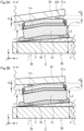
- FIGS. 3A-B are schematic cross-sectional views of main portions of the semiconductor device according to the embodiment.
- FIGS. 3A-B the distance L 1 between the first side 11b and the bottom surface 1 is shorter than the distance L 2 between the second side 11c and the bottom surface 1.
- FIG. 3A shows that a film thickness t 3 of the second bonding material 20 in the vicinity of the first side 11b is thinner than a film thickness t 4 of the second bonding material 20 in the vicinity of the second side 11c.
- FIG. 3B shows that the film thickness t 3 of the second bonding material 20 in the vicinity of the first side 11b is thicker than the film thickness t 4 of the second bonding material 20 in the vicinity of the second side 11c. Both cases above can be preferably used as the semiconductor device 100 of the embodiment.
- the film thickness t 3 and the film thickness t 4 are measured perpendicular to the first upper surface 4.
- the manufacturing method of the semiconductor device 100 of the embodiment is described. First, the drain connector 2, the third connector 54, and the fourth connector 64 are disposed on the reflow plate. Then, a cream solder to be the first bonding material 70 is applied on the drain connector 2. Next, the semiconductor chip 10 is disposed on the cream solder to be the first bonding material 70. Next, on the semiconductor chip 10, a creamed solder to be the second bonding material 20 is applied. Next, on the second plate 58 of the third connector 54, a cream solder to be the third bonding material 59 is applied. Next, on the gate electrode of the semiconductor chip 10, a cream solder to be the fourth bonding material 80 is applied.
- a cream solder to be the fifth bonding material 69 is applied on the third plate 68 of the fourth connector 64.
- the first end 51a of the second connector 50 is disposed on the cream solder to be second bonding material 20.
- the second end 51b of the second connector 50 is disposed on the cream solder to be the third bonding material 59.
- the third end 61a of the fifth connector 60 is disposed on the cream solder to be the fourth bonding material 80.
- the fourth end 61b of the fifth connector 60 is disposed on the cream solder to be the fifth bonding material 69.
- the cream solders are heated by a vacuum reflow heat treatment and melted.
- the cream solders are solidified by cooling.
- the first bonding material 70, the second bonding material 20, the third bonding material 59, the fourth bonding material 80, and the fifth bonding material 69 are formed.
- the semiconductor device 100 of the embodiment is obtained.
- the manufacturing method of the semiconductor device 100 of the embodiment are not limited to those described above.
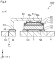
- FIG. 4 is a schematic sectional view of a semiconductor device 1000 as a first comparative embodiment of the embodiment.
- the semiconductor chip 10 does not include the protrusion 11d. Further, in the semiconductor device 1000, the slope 30 is not provided.
- FIG. 5 is a schematic sectional view of a semiconductor device 1100 as a second comparative embodiment of the embodiment.
- the semiconductor chip 10 has the protrusion 11d. Further, in the semiconductor device 1100, the slope 30 is not provided.
- the film thickness of the semiconductor chip is reduced.
- the semiconductor chip is provided with a vertical MOSFET, it is preferable that the film thickness of the semiconductor chip is thin in order to reduce the on-resistance of MOSFET.
- the film thickness of the drain electrode provided on the bottom surface of the semiconductor chip and the film thickness of the source electrode provided on the upper surface of the semiconductor chip becomes relatively thick. Therefore, the semiconductor chip becomes susceptible to the effects of the stress of the drain electrode and the source electrode. In particular, the semiconductor chip often warps upwards convexly. Therefore, how to connect the connectors to such semiconductor chip has become an issue.
- the cream solder is melted and solidified by vacuum-reflow heat treatment.
- bubbles may enter the inside of the cream solder.
- the part with such void is more thermally resistive than the part of the surrounding bonding material. Therefore, how to remove the void has become an issue.
- the third connector 54 Since the third connector 54 is provided, evacuation conductance between the semiconductor chip 10 and the third connector 54 is reduced in the vacuum-reflow, and the void 22a of the second bonding material 20 near the third connector 54 is hardly pulled out.
- the semiconductor chip 10 has a protrusion 11d
- the gap between the semiconductor chip 10 and the second connector 50 in the side close to the third connector 54 is narrowed.
- the void is hardly pulled out further.
- the film thickness of the first bonding material 70 and the film thickness of the second bonding material 20 become uneven. As described above, when the thickness of the bonding material is uneven, the bonding material is easily cracked due to thermal cycling applied to the semiconductor device 100 due to heating and cooling of the semiconductor device 100.
- the drain connector 2 whose plate thickness of the first plate portion 3a of first plate 3 is thinner than the plate thickness of the second plate portion 3b provided between the first plate portion 3a and the drain connector 6 is used.
- the drain connector 2 whose plate thickness of the first plate portion 3a of first plate 3 is thinner than the plate thickness of the second plate portion 3b provided between the first plate portion 3a and the drain connector 6 is used.
- the second bonding material 20 provided on the side of the first plate portion 3a is melted earlier than the second bonding material 20 provided on the side of the second plate portion 3b. This makes it difficult to form the void on the side of the first plate portion 3a of the second bonding material 20, that is, on the side close to the third connector 54.
- variations in the thickness of the second bonding material 20 can be reduced, and the thickness of the second bonding material 20 can be made more uniform. Therefore, cracks in the second bonding material 20 hardly enter.
- the slope 30 can be easily and accurately formed using a mold. Further, the slope 30 can hold the semiconductor chip stably via the first bonding material 70. Therefore, the slope 30 is preferably used in the semiconductor device 100 of the embodiment.
- the area of the slope 30 when viewed from above is preferably larger than the area of the semiconductor chip 10 when viewed from above. This is because it is possible to hold the semiconductor chip 10 stably when the area of the slope 30 is larger.
- the angle ⁇ between the second upper surface 32 and the first upper surface 4 is preferably 0.2 degrees or more and 3 degrees or less. If ⁇ is less than 0.2 degrees, since the gap between the semiconductor chip 10 and the second connector 50 is not sufficiently uniform, the void 22 formed within the second bonding material 20 is hardly pulled out. On the other hand, if ⁇ is greater than 3 degrees, the film thickness of the second bonding material 20 closer to the drain terminal 6 becomes too thin, and it is difficult to pull out the void 22.
- the diameter of the void 22 is preferably 1mm or less, in order to reduce the thermal resistance of semiconductor device 100 as much as possible.
- FIG. 6 is a schematic cross-sectional view of a semiconductor device 1200 as a third comparative embodiment of the embodiment. It is considered to make the thickness of the second bonding material 20 more uniform by connecting the connector extension 55 to the second end 51b. However, the cross-sectional area of the connector extension 55 in a plane parallel to the XY plane is small. Therefore, as in the semiconductor device 100 of the embodiment, it is preferable that the plate thickness of the first plate portion 3a of the first plate 3 is thinner than the plate thickness of the second plate portion 3b of the first plate 3 provided between the first plate portion 3a and the drain terminal 6. This is because it is possible to ensure a larger cross-sectional area by using such drain connector 2. Further, it is possible to improve the contact with the semiconductor chip 10. Therefore, it is possible to reduce the thermal resistance of the semiconductor device.
- the semiconductor device of the embodiment it is possible to provide a semiconductor device having high reliability.
Landscapes
- Wire Bonding (AREA)
- Electrodes Of Semiconductors (AREA)
Abstract
Description
- This application is based upon and claims the benefit of priority from
Japanese Patent Application No.2022-045800, filed on March 22, 2022 - Embodiments described herein relate generally to semiconductor device.
- A semiconductor device having a semiconductor chip such as a metal oxide semiconductor field effect transistor (MOSFET) is used for applications such as power conversion. For example, when semiconductor device described above is a vertical MOSFET, a source electrode provided on an upper surface of a semiconductor chip is connected to a connector provided on MOSFET, for example.
-
-
FIG. 1 is a schematic top view of a semiconductor device according to an embodiment; -
FIG. 2 is a schematic cross-sectional view of the semiconductor device according to the embodiment; -
FIGS. 3A-B are schematic cross-sectional views of main portions of the semiconductor device according to the embodiment; -
FIG.4 is a schematic sectional view of a semiconductor device as a first comparative embodiment of the embodiment; -
FIG.5 is a schematic sectional view of a semiconductor device as a second comparative embodiment of the embodiment; and -
FIG.6 is a schematic sectional view of a semiconductor device as a third comparative embodiment of the embodiment. - Hereinafter, embodiments of the present disclosure will be described with reference to the drawings. Note that in the following description, the same members and the like are denoted by the same reference numerals, and description of members and the like once described is appropriately omitted.
- In this specification, in order to illustrate the positional relationship of parts and the like, the upward direction of the drawings may be referred to as "upper", and the downward direction of the drawings may be referred to as "lower". Here, the terms "up" and "down" do not necessarily indicate a relationship with the direction of gravity.
- A semiconductor device of embodiments includes: a first connector including a first plate having a first upper surface and a first terminal connected to the first plate, a first plate including a second plate and a third plate, a plate thickness of the second plate being thinner than a plate thickness of the third plate, the third plate being provided between the second plate and the first terminal; a semiconductor chip provided on the first upper surface; a first bonding material provided between the first upper surface and the semiconductor chip; a second connector provided on the semiconductor chip, a third connector, the first plate being provided between the first terminal and the third connector; a second bonding material provided between the second connector and the semiconductor chip; and a third bonding material provided between the second connector and the third connector.
-
FIG. 1 is a schematic top view of asemiconductor device 100 according to the embodiment.FIG. 2 is a schematic cross-sectional view of thesemiconductor device 100 of the embodiment.FIG. 2 is a schematic view of a cross section taken along line A-A' inFIG. 1 . - With reference to
FIGS. 1 and2 , thesemiconductor device 100 of the embodiment is explained. - A drain connector (die pad, an example of the first connector) 2 is a member containing a conductive material such as Cu (copper), and a
semiconductor chip 10 is disposed on thedrain connector 2. Thedrain connector 2 has a first plate (an example of a plate) 3 and drain terminals (the drain terminal is an example of a first terminal) 6. Thefirst plate 3 has a bottom surface 1 and a firstupper surface 4. Thedrain terminal 6 is connected to thefirst plate 3. Thedrain terminal 6 is used to connect thesemiconductor chip 10 and an external circuit (not shown). - Here, an X direction, a Y direction perpendicular to the X direction, and a Z direction perpendicular to the X direction and the Y direction are defined. The bottom surface 1 and the first
upper surface 4 are disposed parallel to the XY plane. Thedrain terminal 6 is provided on the Y-direction side of thefirst plate 3. - The
first plate 3 has a first plate portion (an example of a second plate) 3a and a second plate portion (an example of a third plate) 3b. Thesecond plate portion 3b is provided between thefirst plate portion 3a and thedrain terminal 6. A film thickness t1 of thefirst plate portion 3a of thefirst plate 3 is thinner than a film thickness t2 of thesecond plate portion 3b of thefirst plate 3. Here, the film thickness t1 and the film thickness t2 are measured perpendicular to the firstupper surface 4. - For example, the first
upper surface 4 has aslope 30 on the firstupper surface 4. Theslope 30 is provided so as to be lower from thesecond plate portion 3b toward thefirst plate portion 3a. Theslope 30 has a secondupper surface 32. - The angle θ formed by the second
upper surface 32 and the firstupper surface 4 is preferably 0.2 degrees or more and 3 degrees or less. In the figure of the embodiment, in order to illustrateslope 30 easily, it is illustrated with θ greater than 3 degrees. - The
semiconductor chip 10 is provided on (above) the firstupper surface 4 of thedrain connector 2 or on theslope 30 of thedrain connector 2. Thesemiconductor chip 10 is, for example, a chip in which the vertical MOSFET or an IGBT (Insulated Gate Bipolar Transistor) or the like is provided on a semiconductor substrate such as a Si (silicon) substrate, an SiC (silicon carbide) substrate, a GaAs (gallium arsenide) substrate, or a GaN (gallium nitride) substrate. - As shown in
FIG. 2 , thesemiconductor chip 10 of the embodiment has aprotrusion 11d. Thesemiconductor chip 10 of the embodiment has a convex shape on top. In thesemiconductor device 100, theprotrusion 11d is disposed so as to be convex upward. In other words, theprotrusion 11d has a convex shape on the second metal film (source electrode) 18 side. That is, thesemiconductor chip 10 has a convex shape on the side where asecond connector 50 is provided. Note that thesemiconductor chip 10 which does not have an upwardly convex configuration can be preferably used insemiconductor device 100 of the embodiment. - The
semiconductor chip 10 has a thirdupper surface 11a. The thirdupper surface 11a has afirst side 11b and asecond side 11c facing thefirst side 11b. When viewed from above, thefirst side 11b is provided between thesecond side 11c and thethird connector 54. - A
first bonding material 70 is provided between the firstupper surface 4 and thesemiconductor chip 10. When the firstupper surface 4 has theslope 30, thefirst bonding material 70 is provided between theslope 30 and thesemiconductor chip 10. Thefirst bonding material 70 joins the firstupper surface 4 orslope 30 and thesemiconductor chip 10. For example, when thesemiconductor chip 10 is provided with the MOSFET, thefirst bonding material 70 joins the firstupper surface 4 or theslope 30 and the drain electrode (not shown) of thesemiconductor chip 10. - The area of the
slope 30 when viewed from above is preferably larger than the area of thesemiconductor chip 10 when viewed from above. - Incidentally, the
slope 30 may be provided on the entire surface on the firstupper surface 4, or theslope 30 may be provided on a portion of the firstupper surface 4. - The
first bonding material 70 may have a void 72 in thefirst bonding material 70. InFIG. 2 , avoid 72a and avoid 72b are shown. - The
first metal film 16 is provided on thesemiconductor chip 10. Thefirst metal film 16 includes, for example, Al (aluminum). - An
insulating film 12 is provided on thefirst metal film 16. For example, the insulatingfilm 12 is provided on the end of thesemiconductor chip 10 and on the end of thefirst metal film 16. The insulatingfilm 12 includes insulating materials such as polyimides. - A
second metal film 18 is provided on thefirst metal film 16. Thesecond metal film 18 is surrounded by the insulatingfilm 12 on thefirst metal film 16. Thesecond metal film 18 includes, for example, Ni and Au. - For example, when the
semiconductor chip 10 is provided with the MOSFET, thefirst metal film 16 and thesecond metal film 18 correspond to the source electrode of the MOSFET. - A third connector (an example of a first post) 54 has a
second plate 58 and source terminals (the source terminal is an example of a second terminal) 56. Thethird connector 54 includes a conductive material such as Cu. Thethird connector 54 is used for connecting thesemiconductor chip 10 and an external circuit (not shown). Here, thefirst plate 3 is provided between thedrain terminal 6 and thesource terminal 56. Further, thesecond plate 58 is, for example, provided between thesource terminal 56 and thefirst plate 3. - A fourth connector (an example of a second post) 64 has a
third plate 68 and agate terminal 66. Thefourth connector 64 includes a conductive material such as Cu. Thefourth connector 64 is used for connecting thesemiconductor chip 10 and an external circuit (not shown). - The
second connector 50 includes afirst end 51a and asecond end 51b. Thesecond connector 50 includes, for example, a conductive material such as Cu. Incidentally, the surface of thesecond connector 50 may be plated by a material containing, for example, Sn. Thefirst end 51a is provided above thefirst metal film 16. Thesecond end 51b is provided on thesecond plate 58. - A
second bonding material 20 is provided on thesecond metal film 18. Thesecond bonding material 20 is provided between thesecond metal film 18 and thefirst end 51a. Thesecond bonding material 20 joins thefirst end 51a and thesecond metal film 18. - The
second bonding material 20 may have a void (bubble) 22 in thesecond bonding material 20. InFIG. 2 , a void 22a and a void 22b are shown. - The diameter of the void 22 is preferably 1mm or less. It is further preferable that the void 22 has a diameter of 500µm or less.
- The
third bonding material 59 is provided between thesecond plate 58 and thesecond end 51b. Thethird bonding material 59 joins thesecond plate 58 and the second end 51. - The
fifth connector 60 has athird end 61a and afourth end 61b. Thefifth connector 60 includes, for example, a conductive material such as Cu. Incidentally, the surface of thefifth connector 60 may be plated by a material containing, for example, Sn. Thethird end 61a is electrically connected to thesemiconductor chip 10 via afourth bonding material 80 provided on thesemiconductor chip 10. Below thefourth bonding material 80, for example, a gate electrode (not shown) of thesemiconductor chip 10 is provided. - The
fifth bonding material 69 is provided between thethird plate 68 and thefourth end 61b. Thefifth bonding material 69 joins thethird plate 68 and thefourth end 61b. - When the
semiconductor chip 10 has theprotrusion 11d, the film thickness of thefirst bonding material 70 near the center of thesemiconductor chip 10 is thick. On the other hand, the film thickness of thefirst bonding material 70 near the end of thesemiconductor chip 10 is thin. Here, the film thickness of thefirst bonding material 70 is measured perpendicular to the firstupper surface 4. - When the
semiconductor chip 10 has theprotrusion 11d, the film thickness of thesecond bonding material 20 near the center of thesemiconductor chip 10 is thin. On the other hand, the film thickness of thesecond bonding material 20 near the end ofsemiconductor chip 10 is thick. Here, the film thickness of the second bonding material is measured perpendicular to the firstupper surface 4. - As the
first bonding material 70, thesecond bonding material 20, thethird bonding material 59, thefourth bonding material 80, and thefifth bonding material 69, for example, solder containing Pb (lead) and Sn (tin), solder containing Pb, Ag (silver), and Sn (tin), solder containing Sn and Sb (antimony), solder containing Au (gold) and Sn, solder containing Au and Si, or solder containing Au and Ge (germanium) can be preferably used. -
FIGS. 3A-B are schematic cross-sectional views of main portions of the semiconductor device according to the embodiment. - As shown in
FIGS. 3A-B , the distance L1 between thefirst side 11b and the bottom surface 1 is shorter than the distance L2 between thesecond side 11c and the bottom surface 1.FIG. 3A shows that a film thickness t3 of thesecond bonding material 20 in the vicinity of thefirst side 11b is thinner than a film thickness t4 of thesecond bonding material 20 in the vicinity of thesecond side 11c.FIG. 3B shows that the film thickness t3 of thesecond bonding material 20 in the vicinity of thefirst side 11b is thicker than the film thickness t4 of thesecond bonding material 20 in the vicinity of thesecond side 11c. Both cases above can be preferably used as thesemiconductor device 100 of the embodiment. Here, the film thickness t3 and the film thickness t4 are measured perpendicular to the firstupper surface 4. - The manufacturing method of the
semiconductor device 100 of the embodiment is described. First, thedrain connector 2, thethird connector 54, and thefourth connector 64 are disposed on the reflow plate. Then, a cream solder to be thefirst bonding material 70 is applied on thedrain connector 2. Next, thesemiconductor chip 10 is disposed on the cream solder to be thefirst bonding material 70. Next, on thesemiconductor chip 10, a creamed solder to be thesecond bonding material 20 is applied. Next, on thesecond plate 58 of thethird connector 54, a cream solder to be thethird bonding material 59 is applied. Next, on the gate electrode of thesemiconductor chip 10, a cream solder to be thefourth bonding material 80 is applied. Next, on thethird plate 68 of thefourth connector 64, a cream solder to be thefifth bonding material 69 is applied. Next, thefirst end 51a of thesecond connector 50 is disposed on the cream solder to besecond bonding material 20. Next, thesecond end 51b of thesecond connector 50 is disposed on the cream solder to be thethird bonding material 59. Next, thethird end 61a of thefifth connector 60 is disposed on the cream solder to be thefourth bonding material 80. Next, thefourth end 61b of thefifth connector 60 is disposed on the cream solder to be thefifth bonding material 69. Next, the cream solders are heated by a vacuum reflow heat treatment and melted. Next, the cream solders are solidified by cooling. Thus, thefirst bonding material 70, thesecond bonding material 20, thethird bonding material 59, thefourth bonding material 80, and thefifth bonding material 69 are formed. Thus, thesemiconductor device 100 of the embodiment is obtained. The manufacturing method of thesemiconductor device 100 of the embodiment are not limited to those described above. - Next, the operation and effects of semiconductor device of the embodiment will be described.
-
FIG. 4 is a schematic sectional view of asemiconductor device 1000 as a first comparative embodiment of the embodiment. Thesemiconductor chip 10 does not include theprotrusion 11d. Further, in thesemiconductor device 1000, theslope 30 is not provided. -
FIG. 5 is a schematic sectional view of asemiconductor device 1100 as a second comparative embodiment of the embodiment. Thesemiconductor chip 10 has theprotrusion 11d. Further, in thesemiconductor device 1100, theslope 30 is not provided. - It is preferable to reduce the film thickness of the semiconductor chip. For example, if the semiconductor chip is provided with a vertical MOSFET, it is preferable that the film thickness of the semiconductor chip is thin in order to reduce the on-resistance of MOSFET. However, in this case, the film thickness of the drain electrode provided on the bottom surface of the semiconductor chip and the film thickness of the source electrode provided on the upper surface of the semiconductor chip becomes relatively thick. Therefore, the semiconductor chip becomes susceptible to the effects of the stress of the drain electrode and the source electrode. In particular, the semiconductor chip often warps upwards convexly. Therefore, how to connect the connectors to such semiconductor chip has become an issue.
- In addition, during the production of the semiconductor device, the cream solder is melted and solidified by vacuum-reflow heat treatment. Here, when the cream solder melts, bubbles (void) may enter the inside of the cream solder. The part with such void is more thermally resistive than the part of the surrounding bonding material. Therefore, how to remove the void has become an issue.
- Since the
third connector 54 is provided, evacuation conductance between thesemiconductor chip 10 and thethird connector 54 is reduced in the vacuum-reflow, and the void 22a of thesecond bonding material 20 near thethird connector 54 is hardly pulled out. In particular, when thesemiconductor chip 10 has aprotrusion 11d, the gap between thesemiconductor chip 10 and thesecond connector 50 in the side close to thethird connector 54 is narrowed. Thus, the void is hardly pulled out further. - Further, when the
semiconductor chip 10 has theprotrusion 11d, compared with the case when thesemiconductor chip 10 does not have theprotrusion 11d, the film thickness of thefirst bonding material 70 and the film thickness of thesecond bonding material 20 become uneven. As described above, when the thickness of the bonding material is uneven, the bonding material is easily cracked due to thermal cycling applied to thesemiconductor device 100 due to heating and cooling of thesemiconductor device 100. - Therefore, in the
semiconductor device 100, thedrain connector 2 whose plate thickness of thefirst plate portion 3a offirst plate 3 is thinner than the plate thickness of thesecond plate portion 3b provided between thefirst plate portion 3a and thedrain connector 6 is used. Thus, it is possible to equalize the gap between thesemiconductor chip 10 and thesecond connector 50 more. Therefore, when performing vacuum-reflow, the void formed in thesecond bonding material 20 is likely to come off. - Further, since the heat capacity of the
first plate portion 3a is smaller than the heat capacity of thesecond plate portion 3b, thesecond bonding material 20 provided on the side of thefirst plate portion 3a is melted earlier than thesecond bonding material 20 provided on the side of thesecond plate portion 3b. This makes it difficult to form the void on the side of thefirst plate portion 3a of thesecond bonding material 20, that is, on the side close to thethird connector 54. - In addition, variations in the thickness of the
second bonding material 20 can be reduced, and the thickness of thesecond bonding material 20 can be made more uniform. Therefore, cracks in thesecond bonding material 20 hardly enter. - The
slope 30 can be easily and accurately formed using a mold. Further, theslope 30 can hold the semiconductor chip stably via thefirst bonding material 70. Therefore, theslope 30 is preferably used in thesemiconductor device 100 of the embodiment. - The area of the
slope 30 when viewed from above is preferably larger than the area of thesemiconductor chip 10 when viewed from above. This is because it is possible to hold thesemiconductor chip 10 stably when the area of theslope 30 is larger. - The angle θ between the second
upper surface 32 and the firstupper surface 4 is preferably 0.2 degrees or more and 3 degrees or less. If θ is less than 0.2 degrees, since the gap between thesemiconductor chip 10 and thesecond connector 50 is not sufficiently uniform, the void 22 formed within thesecond bonding material 20 is hardly pulled out. On the other hand, if θ is greater than 3 degrees, the film thickness of thesecond bonding material 20 closer to thedrain terminal 6 becomes too thin, and it is difficult to pull out the void 22. - The diameter of the void 22 is preferably 1mm or less, in order to reduce the thermal resistance of
semiconductor device 100 as much as possible. -
FIG. 6 is a schematic cross-sectional view of asemiconductor device 1200 as a third comparative embodiment of the embodiment. It is considered to make the thickness of thesecond bonding material 20 more uniform by connecting the connector extension 55 to thesecond end 51b. However, the cross-sectional area of the connector extension 55 in a plane parallel to the XY plane is small. Therefore, as in thesemiconductor device 100 of the embodiment, it is preferable that the plate thickness of thefirst plate portion 3a of thefirst plate 3 is thinner than the plate thickness of thesecond plate portion 3b of thefirst plate 3 provided between thefirst plate portion 3a and thedrain terminal 6. This is because it is possible to ensure a larger cross-sectional area by usingsuch drain connector 2. Further, it is possible to improve the contact with thesemiconductor chip 10. Therefore, it is possible to reduce the thermal resistance of the semiconductor device. - According to the semiconductor device of the embodiment, it is possible to provide a semiconductor device having high reliability.
- While certain embodiments have been described, these embodiments have been presented by way of example only, and are not intended to limit the scope of the inventions. Indeed, the semiconductor device described herein may be embodied in a variety of other forms; furthermore, various omissions, substitutions and changes in the form of the devices and methods described herein may be made without departing from the spirit of the inventions. The accompanying claims and their equivalents are intended to cover such forms or modifications as would fall within the scope and spirit of the inventions.
- It is explicitly stated that all features disclosed in the description and/or the claims are intended to be disclosed separately and independently from each other for the purpose of original disclosure as well as for the purpose of restricting the claimed invention independent of the composition of the features in the embodiments and/or the claims. It is explicitly stated that all value ranges or indications of groups of entities disclose every possible intermediate value or intermediate entity for the purpose of original disclosure as well as for the purpose of restricting the claimed invention, in particular as limits of value ranges.
Claims (9)
- A semiconductor device (100), comprising:a first connector (2) including a first plate (3) having a first upper surface (4) and a first terminal (6) connected to the first plate (3), a first plate (3) including a second plate (3a) and a third plate (3b), a plate thickness of the second plate (3a) being thinner than a plate thickness of the third plate(3b), the third plate (3b) being provided between the second plate (3a) and the first terminal (6);a semiconductor chip (10) provided on the first upper surface (4);a first bonding material (70) provided between the first upper surface (4) and the semiconductor chip (10);a second connector (50) provided on the semiconductor chip (10),a third connector (54), the first plate (3) being provided between the first terminal (6) and the third connector (54);a second bonding material (20) provided between the second connector (50) and the semiconductor chip (10); anda third bonding material (59) provided between the second connector (50) and the third connector (54).
- The semiconductor device (100) according to claim 1,
wherein the semiconductor chip (10) has a convex shape on the side where the second connector (50) is provided. - The semiconductor device (100) according to claim 1 or 2,
wherein the first upper surface (4) has a slope (30) on the first upper surface (4), and the slope (30) is lowered from the third plate (3b) toward the second plate (3a). - The semiconductor device (100) according to claim 3,
wherein an area of the slope (30) when viewed from above is larger than an area of the semiconductor chip (10) when viewed from above. - The semiconductor device according to claim 3 or 4,
wherein an angle formed by the second upper surface (32) of the slope (30) and the first upper surface (4) is preferably 0.2 degrees or more and 3 degrees or less. - The semiconductor device (100) according to any one of claims 1 to 5,
wherein the second bonding material (20) has a void (72). - The semiconductor device (100) according to claim 6,
wherein a diameter of the void (72) is 1mm or less. - The semiconductor device (100) according to any one of claims 1 to 7,wherein a third upper surface (11a) of the semiconductor chip (10) has a first side (11b) and a second side (11c) facing the first side (11b),wherein, when viewed from above, the first side (11b) is provided between the second side (11c) and the third connector (54), andwherein a thickness of the second bonding material (20) in the vicinity of the first side (11b) is thinner than a thickness of the second bonding material (20) in the vicinity of the second side (11c).
- The semiconductor device (100) according to any one of claims 1 to 7,wherein a third upper surface (11a) of the semiconductor chip (10) has a first side (11b) and a second side (11c) facing the first side (11b),wherein, when viewed from above, the first side (11b) is provided between the second side (11c) and the third connector (54), andwherein a thickness of the second bonding material (20) in the vicinity of the first side (11b) is thicker than a thickness of the second bonding material (20) in the vicinity of the second side (11c).
Applications Claiming Priority (1)
| Application Number | Priority Date | Filing Date | Title |
|---|---|---|---|
| JP2022045800A JP7703475B2 (en) | 2022-03-22 | 2022-03-22 | Semiconductor Device |
Publications (2)
| Publication Number | Publication Date |
|---|---|
| EP4250354A1 true EP4250354A1 (en) | 2023-09-27 |
| EP4250354B1 EP4250354B1 (en) | 2024-10-09 |
Family
ID=83508650
Family Applications (1)
| Application Number | Title | Priority Date | Filing Date |
|---|---|---|---|
| EP22194500.9A Active EP4250354B1 (en) | 2022-03-22 | 2022-09-08 | Semiconductor device |
Country Status (4)
| Country | Link |
|---|---|
| US (1) | US12469816B2 (en) |
| EP (1) | EP4250354B1 (en) |
| JP (1) | JP7703475B2 (en) |
| CN (1) | CN116825842A (en) |
Citations (3)
| Publication number | Priority date | Publication date | Assignee | Title |
|---|---|---|---|---|
| US20150262917A1 (en) * | 2014-03-12 | 2015-09-17 | Kabushiki Kaisha Toshiba | Semiconductor device and method of manufacturing the same |
| US20160204047A1 (en) * | 2014-01-20 | 2016-07-14 | Denso Corporation | Semiconductor device and method for manufacturing the same |
| US20200168575A1 (en) * | 2018-11-28 | 2020-05-28 | Infineon Technologies Ag | Semiconductor Device and Method for Fabricating a Semiconductor Device |
Family Cites Families (24)
| Publication number | Priority date | Publication date | Assignee | Title |
|---|---|---|---|---|
| US5866818A (en) * | 1995-11-30 | 1999-02-02 | Matsushita Electric Works, Ltd. | Acceleration sensor device |
| EP1387146A3 (en) * | 2002-07-29 | 2006-05-31 | Yamaha Corporation | Manufacturing method for magnetic sensor and lead frame therefor |
| JP2004111745A (en) * | 2002-09-19 | 2004-04-08 | Toshiba Corp | Semiconductor device |
| JP2005117009A (en) * | 2003-09-17 | 2005-04-28 | Denso Corp | Semiconductor device and manufacturing method thereof |
| US20050225222A1 (en) * | 2004-04-09 | 2005-10-13 | Joseph Mazzochette | Light emitting diode arrays with improved light extraction |
| JP4468115B2 (en) | 2004-08-30 | 2010-05-26 | 株式会社ルネサステクノロジ | Semiconductor device |
| US7290448B2 (en) * | 2004-09-10 | 2007-11-06 | Yamaha Corporation | Physical quantity sensor, lead frame, and manufacturing method therefor |
| WO2006040987A1 (en) * | 2004-10-08 | 2006-04-20 | Yamaha Corporation | Method of producing physical quantity sensor |
| US7359416B2 (en) * | 2006-03-15 | 2008-04-15 | Matsushita Electric Industrial Co., Ltd. | Optical semiconductor device |
| US20100075465A1 (en) * | 2008-09-25 | 2010-03-25 | Silverbrook Research Pty Ltd | Method of reducing voids in encapsulant |
| KR20120005341A (en) * | 2010-07-08 | 2012-01-16 | 주식회사 하이닉스반도체 | Semiconductor Chips & Packages |
| JP5651430B2 (en) * | 2010-10-29 | 2015-01-14 | 新電元工業株式会社 | Electronic component mounting method |
| KR20140009799A (en) * | 2012-07-13 | 2014-01-23 | 에스케이하이닉스 주식회사 | Package of electronic device and method for manufacturing the same |
| JP2015012065A (en) * | 2013-06-27 | 2015-01-19 | 株式会社デンソー | Manufacturing method of semiconductor device |
| DE102013113009A1 (en) * | 2013-11-25 | 2015-05-28 | Osram Opto Semiconductors Gmbh | Housing for a semiconductor chip, housing composite, semiconductor device and method for producing a semiconductor device |
| US10431528B2 (en) * | 2016-02-08 | 2019-10-01 | Mitsubishi Electric Corporation | Semiconductor device |
| JP2019054069A (en) * | 2017-09-14 | 2019-04-04 | 株式会社東芝 | Semiconductor device |
| JP2019087613A (en) | 2017-11-06 | 2019-06-06 | トヨタ自動車株式会社 | Method of manufacturing semiconductor device |
| US11270929B2 (en) * | 2018-01-05 | 2022-03-08 | Mitsubishi Electric Corporation | Semiconductor device |
| JP6447946B1 (en) | 2018-01-19 | 2019-01-09 | パナソニックIpマネジメント株式会社 | Semiconductor device and semiconductor module |
| JP7199823B2 (en) * | 2018-04-12 | 2023-01-06 | 新電元工業株式会社 | Semiconductor device and method for manufacturing semiconductor device |
| JP7090579B2 (en) * | 2019-05-08 | 2022-06-24 | 三菱電機株式会社 | Semiconductor devices and their manufacturing methods |
| US11101417B2 (en) * | 2019-08-06 | 2021-08-24 | X Display Company Technology Limited | Structures and methods for electrically connecting printed components |
| JP2021034615A (en) | 2019-08-27 | 2021-03-01 | 株式会社デンソー | Semiconductor device |
-
2022
- 2022-03-22 JP JP2022045800A patent/JP7703475B2/en active Active
- 2022-08-03 CN CN202210925224.8A patent/CN116825842A/en active Pending
- 2022-09-02 US US17/902,535 patent/US12469816B2/en active Active
- 2022-09-08 EP EP22194500.9A patent/EP4250354B1/en active Active
Patent Citations (3)
| Publication number | Priority date | Publication date | Assignee | Title |
|---|---|---|---|---|
| US20160204047A1 (en) * | 2014-01-20 | 2016-07-14 | Denso Corporation | Semiconductor device and method for manufacturing the same |
| US20150262917A1 (en) * | 2014-03-12 | 2015-09-17 | Kabushiki Kaisha Toshiba | Semiconductor device and method of manufacturing the same |
| US20200168575A1 (en) * | 2018-11-28 | 2020-05-28 | Infineon Technologies Ag | Semiconductor Device and Method for Fabricating a Semiconductor Device |
Also Published As
| Publication number | Publication date |
|---|---|
| CN116825842A (en) | 2023-09-29 |
| US12469816B2 (en) | 2025-11-11 |
| US20230317672A1 (en) | 2023-10-05 |
| JP2023139980A (en) | 2023-10-04 |
| EP4250354B1 (en) | 2024-10-09 |
| JP7703475B2 (en) | 2025-07-07 |
Similar Documents
| Publication | Publication Date | Title |
|---|---|---|
| CN100589243C (en) | Semiconductor device | |
| TWI395277B (en) | Wafer level wafer level packaging | |
| EP4250353A1 (en) | Semiconductor device | |
| US20090008804A1 (en) | Power semiconductor package | |
| US10727209B2 (en) | Semiconductor device and semiconductor element with improved yield | |
| TW201240031A (en) | Microelectronic packages with enhanced heat dissipation and methods of manufacturing | |
| US9859195B1 (en) | Semiconductor device | |
| US11164841B2 (en) | Semiconductor device | |
| CN108206141A (en) | The manufacturing method of semiconductor device | |
| EP4250354B1 (en) | Semiconductor device | |
| US11784167B2 (en) | Semiconductor device with metal film having openings | |
| CN100435328C (en) | molded package | |
| WO2017157486A1 (en) | Semiconductor device | |
| WO2021140771A1 (en) | Semiconductor device | |
| CN112447671A (en) | Interconnection fixture with inclined contact surfaces and raised bridges | |
| CN113363228A (en) | Semiconductor device with a plurality of semiconductor chips | |
| JP6462609B2 (en) | Semiconductor device | |
| EP4246572A1 (en) | Semiconductor device | |
| US11823985B2 (en) | Leadframe, semiconductor device, and method for manufacturing semiconductor device | |
| JP2022143657A (en) | Semiconductor device and manufacturing method thereof | |
| US20250285945A1 (en) | Semiconductor device including a lead and a sealing resin | |
| WO2025220148A1 (en) | Power semiconductor device and method for manufacturing same | |
| TW202324617A (en) | Semiconductor device | |
| JP2024038590A (en) | Semiconductor device and semiconductor device manufacturing method |
Legal Events
| Date | Code | Title | Description |
|---|---|---|---|
| PUAI | Public reference made under article 153(3) epc to a published international application that has entered the european phase |
Free format text: ORIGINAL CODE: 0009012 |
|
| STAA | Information on the status of an ep patent application or granted ep patent |
Free format text: STATUS: REQUEST FOR EXAMINATION WAS MADE |
|
| 17P | Request for examination filed |
Effective date: 20220908 |
|
| AK | Designated contracting states |
Kind code of ref document: A1 Designated state(s): AL AT BE BG CH CY CZ DE DK EE ES FI FR GB GR HR HU IE IS IT LI LT LU LV MC MK MT NL NO PL PT RO RS SE SI SK SM TR |
|
| GRAP | Despatch of communication of intention to grant a patent |
Free format text: ORIGINAL CODE: EPIDOSNIGR1 |
|
| STAA | Information on the status of an ep patent application or granted ep patent |
Free format text: STATUS: GRANT OF PATENT IS INTENDED |
|
| RAP3 | Party data changed (applicant data changed or rights of an application transferred) |
Owner name: TOSHIBA ELECTRONIC DEVICES & STORAGE CORPORATION Owner name: KABUSHIKI KAISHA TOSHIBA |
|
| INTG | Intention to grant announced |
Effective date: 20240528 |
|
| GRAS | Grant fee paid |
Free format text: ORIGINAL CODE: EPIDOSNIGR3 |
|
| GRAA | (expected) grant |
Free format text: ORIGINAL CODE: 0009210 |
|
| STAA | Information on the status of an ep patent application or granted ep patent |
Free format text: STATUS: THE PATENT HAS BEEN GRANTED |
|
| AK | Designated contracting states |
Kind code of ref document: B1 Designated state(s): AL AT BE BG CH CY CZ DE DK EE ES FI FR GB GR HR HU IE IS IT LI LT LU LV MC MK MT NL NO PL PT RO RS SE SI SK SM TR |
|
| REG | Reference to a national code |
Ref country code: CH Ref legal event code: EP |
|
| REG | Reference to a national code |
Ref country code: DE Ref legal event code: R096 Ref document number: 602022006653 Country of ref document: DE |
|
| REG | Reference to a national code |
Ref country code: IE Ref legal event code: FG4D |
|
| REG | Reference to a national code |
Ref country code: LT Ref legal event code: MG9D |
|
| REG | Reference to a national code |
Ref country code: NL Ref legal event code: MP Effective date: 20241009 |
|
| REG | Reference to a national code |
Ref country code: AT Ref legal event code: MK05 Ref document number: 1731556 Country of ref document: AT Kind code of ref document: T Effective date: 20241009 |
|
| PG25 | Lapsed in a contracting state [announced via postgrant information from national office to epo] |
Ref country code: NL Free format text: LAPSE BECAUSE OF FAILURE TO SUBMIT A TRANSLATION OF THE DESCRIPTION OR TO PAY THE FEE WITHIN THE PRESCRIBED TIME-LIMIT Effective date: 20241009 |
|
| PG25 | Lapsed in a contracting state [announced via postgrant information from national office to epo] |
Ref country code: NL Free format text: LAPSE BECAUSE OF FAILURE TO SUBMIT A TRANSLATION OF THE DESCRIPTION OR TO PAY THE FEE WITHIN THE PRESCRIBED TIME-LIMIT Effective date: 20241009 |
|
| PG25 | Lapsed in a contracting state [announced via postgrant information from national office to epo] |
Ref country code: HR Free format text: LAPSE BECAUSE OF FAILURE TO SUBMIT A TRANSLATION OF THE DESCRIPTION OR TO PAY THE FEE WITHIN THE PRESCRIBED TIME-LIMIT Effective date: 20241009 Ref country code: IS Free format text: LAPSE BECAUSE OF FAILURE TO SUBMIT A TRANSLATION OF THE DESCRIPTION OR TO PAY THE FEE WITHIN THE PRESCRIBED TIME-LIMIT Effective date: 20250209 Ref country code: PT Free format text: LAPSE BECAUSE OF FAILURE TO SUBMIT A TRANSLATION OF THE DESCRIPTION OR TO PAY THE FEE WITHIN THE PRESCRIBED TIME-LIMIT Effective date: 20250210 |
|
| PG25 | Lapsed in a contracting state [announced via postgrant information from national office to epo] |
Ref country code: FI Free format text: LAPSE BECAUSE OF FAILURE TO SUBMIT A TRANSLATION OF THE DESCRIPTION OR TO PAY THE FEE WITHIN THE PRESCRIBED TIME-LIMIT Effective date: 20241009 |
|
| PG25 | Lapsed in a contracting state [announced via postgrant information from national office to epo] |
Ref country code: BG Free format text: LAPSE BECAUSE OF FAILURE TO SUBMIT A TRANSLATION OF THE DESCRIPTION OR TO PAY THE FEE WITHIN THE PRESCRIBED TIME-LIMIT Effective date: 20241009 |
|
| PG25 | Lapsed in a contracting state [announced via postgrant information from national office to epo] |
Ref country code: ES Free format text: LAPSE BECAUSE OF FAILURE TO SUBMIT A TRANSLATION OF THE DESCRIPTION OR TO PAY THE FEE WITHIN THE PRESCRIBED TIME-LIMIT Effective date: 20241009 |
|
| PG25 | Lapsed in a contracting state [announced via postgrant information from national office to epo] |
Ref country code: NO Free format text: LAPSE BECAUSE OF FAILURE TO SUBMIT A TRANSLATION OF THE DESCRIPTION OR TO PAY THE FEE WITHIN THE PRESCRIBED TIME-LIMIT Effective date: 20250109 |
|
| PG25 | Lapsed in a contracting state [announced via postgrant information from national office to epo] |
Ref country code: AT Free format text: LAPSE BECAUSE OF FAILURE TO SUBMIT A TRANSLATION OF THE DESCRIPTION OR TO PAY THE FEE WITHIN THE PRESCRIBED TIME-LIMIT Effective date: 20241009 Ref country code: LV Free format text: LAPSE BECAUSE OF FAILURE TO SUBMIT A TRANSLATION OF THE DESCRIPTION OR TO PAY THE FEE WITHIN THE PRESCRIBED TIME-LIMIT Effective date: 20241009 Ref country code: GR Free format text: LAPSE BECAUSE OF FAILURE TO SUBMIT A TRANSLATION OF THE DESCRIPTION OR TO PAY THE FEE WITHIN THE PRESCRIBED TIME-LIMIT Effective date: 20250110 |
|
| PG25 | Lapsed in a contracting state [announced via postgrant information from national office to epo] |
Ref country code: PL Free format text: LAPSE BECAUSE OF FAILURE TO SUBMIT A TRANSLATION OF THE DESCRIPTION OR TO PAY THE FEE WITHIN THE PRESCRIBED TIME-LIMIT Effective date: 20241009 |
|
| PG25 | Lapsed in a contracting state [announced via postgrant information from national office to epo] |
Ref country code: RS Free format text: LAPSE BECAUSE OF FAILURE TO SUBMIT A TRANSLATION OF THE DESCRIPTION OR TO PAY THE FEE WITHIN THE PRESCRIBED TIME-LIMIT Effective date: 20250109 |
|
| PG25 | Lapsed in a contracting state [announced via postgrant information from national office to epo] |
Ref country code: SM Free format text: LAPSE BECAUSE OF FAILURE TO SUBMIT A TRANSLATION OF THE DESCRIPTION OR TO PAY THE FEE WITHIN THE PRESCRIBED TIME-LIMIT Effective date: 20241009 |
|
| PG25 | Lapsed in a contracting state [announced via postgrant information from national office to epo] |
Ref country code: DK Free format text: LAPSE BECAUSE OF FAILURE TO SUBMIT A TRANSLATION OF THE DESCRIPTION OR TO PAY THE FEE WITHIN THE PRESCRIBED TIME-LIMIT Effective date: 20241009 |
|
| REG | Reference to a national code |
Ref country code: DE Ref legal event code: R097 Ref document number: 602022006653 Country of ref document: DE |
|
| PG25 | Lapsed in a contracting state [announced via postgrant information from national office to epo] |
Ref country code: EE Free format text: LAPSE BECAUSE OF FAILURE TO SUBMIT A TRANSLATION OF THE DESCRIPTION OR TO PAY THE FEE WITHIN THE PRESCRIBED TIME-LIMIT Effective date: 20241009 |
|
| PG25 | Lapsed in a contracting state [announced via postgrant information from national office to epo] |
Ref country code: RO Free format text: LAPSE BECAUSE OF FAILURE TO SUBMIT A TRANSLATION OF THE DESCRIPTION OR TO PAY THE FEE WITHIN THE PRESCRIBED TIME-LIMIT Effective date: 20241009 |
|
| PG25 | Lapsed in a contracting state [announced via postgrant information from national office to epo] |
Ref country code: SK Free format text: LAPSE BECAUSE OF FAILURE TO SUBMIT A TRANSLATION OF THE DESCRIPTION OR TO PAY THE FEE WITHIN THE PRESCRIBED TIME-LIMIT Effective date: 20241009 |
|
| PG25 | Lapsed in a contracting state [announced via postgrant information from national office to epo] |
Ref country code: CZ Free format text: LAPSE BECAUSE OF FAILURE TO SUBMIT A TRANSLATION OF THE DESCRIPTION OR TO PAY THE FEE WITHIN THE PRESCRIBED TIME-LIMIT Effective date: 20241009 |
|
| PG25 | Lapsed in a contracting state [announced via postgrant information from national office to epo] |
Ref country code: IT Free format text: LAPSE BECAUSE OF FAILURE TO SUBMIT A TRANSLATION OF THE DESCRIPTION OR TO PAY THE FEE WITHIN THE PRESCRIBED TIME-LIMIT Effective date: 20241009 |
|
| PLBE | No opposition filed within time limit |
Free format text: ORIGINAL CODE: 0009261 |
|
| STAA | Information on the status of an ep patent application or granted ep patent |
Free format text: STATUS: NO OPPOSITION FILED WITHIN TIME LIMIT |
|
| PG25 | Lapsed in a contracting state [announced via postgrant information from national office to epo] |
Ref country code: SE Free format text: LAPSE BECAUSE OF FAILURE TO SUBMIT A TRANSLATION OF THE DESCRIPTION OR TO PAY THE FEE WITHIN THE PRESCRIBED TIME-LIMIT Effective date: 20241009 |
|
| 26N | No opposition filed |
Effective date: 20250710 |
|
| PGFP | Annual fee paid to national office [announced via postgrant information from national office to epo] |
Ref country code: DE Payment date: 20250702 Year of fee payment: 4 |
|
| PGFP | Annual fee paid to national office [announced via postgrant information from national office to epo] |
Ref country code: FR Payment date: 20250703 Year of fee payment: 4 |
|
| REG | Reference to a national code |
Ref country code: DE Ref legal event code: R079 Ref document number: 602022006653 Country of ref document: DE Free format text: PREVIOUS MAIN CLASS: H01L0023495000 Ipc: H10W0070400000 |
|
| REG | Reference to a national code |
Ref country code: CH Ref legal event code: H13 Free format text: ST27 STATUS EVENT CODE: U-0-0-H10-H13 (AS PROVIDED BY THE NATIONAL OFFICE) Effective date: 20260504 |