EP4250294A1 - Reducing precharge power consumption in a memory array - Google Patents
Reducing precharge power consumption in a memory array Download PDFInfo
- Publication number
- EP4250294A1 EP4250294A1 EP23162966.8A EP23162966A EP4250294A1 EP 4250294 A1 EP4250294 A1 EP 4250294A1 EP 23162966 A EP23162966 A EP 23162966A EP 4250294 A1 EP4250294 A1 EP 4250294A1
- Authority
- EP
- European Patent Office
- Prior art keywords
- cell
- memory device
- precharge
- output node
- memory
- Prior art date
- Legal status (The legal status is an assumption and is not a legal conclusion. Google has not performed a legal analysis and makes no representation as to the accuracy of the status listed.)
- Pending
Links
Images




Classifications
-
- G—PHYSICS
- G11—INFORMATION STORAGE
- G11C—STATIC STORES
- G11C7/00—Arrangements for writing information into, or reading information out from, a digital store
- G11C7/10—Input/output [I/O] data interface arrangements, e.g. I/O data control circuits, I/O data buffers
- G11C7/1048—Data bus control circuits, e.g. precharging, presetting, equalising
-
- G—PHYSICS
- G11—INFORMATION STORAGE
- G11C—STATIC STORES
- G11C11/00—Digital stores characterised by the use of particular electric or magnetic storage elements; Storage elements therefor
- G11C11/21—Digital stores characterised by the use of particular electric or magnetic storage elements; Storage elements therefor using electric elements
- G11C11/34—Digital stores characterised by the use of particular electric or magnetic storage elements; Storage elements therefor using electric elements using semiconductor devices
- G11C11/40—Digital stores characterised by the use of particular electric or magnetic storage elements; Storage elements therefor using electric elements using semiconductor devices using transistors
- G11C11/41—Digital stores characterised by the use of particular electric or magnetic storage elements; Storage elements therefor using electric elements using semiconductor devices using transistors forming static cells with positive feedback, i.e. cells not needing refreshing or charge regeneration, e.g. bistable multivibrator or Schmitt trigger
- G11C11/413—Auxiliary circuits, e.g. for addressing, decoding, driving, writing, sensing, timing or power reduction
- G11C11/417—Auxiliary circuits, e.g. for addressing, decoding, driving, writing, sensing, timing or power reduction for memory cells of the field-effect type
- G11C11/419—Read-write [R-W] circuits
-
- G—PHYSICS
- G11—INFORMATION STORAGE
- G11C—STATIC STORES
- G11C15/00—Digital stores in which information comprising one or more characteristic parts is written into the store and in which information is read-out by searching for one or more of these characteristic parts, i.e. associative or content-addressed stores
- G11C15/04—Digital stores in which information comprising one or more characteristic parts is written into the store and in which information is read-out by searching for one or more of these characteristic parts, i.e. associative or content-addressed stores using semiconductor elements
-
- G—PHYSICS
- G11—INFORMATION STORAGE
- G11C—STATIC STORES
- G11C7/00—Arrangements for writing information into, or reading information out from, a digital store
- G11C7/10—Input/output [I/O] data interface arrangements, e.g. I/O data control circuits, I/O data buffers
- G11C7/1006—Data managing, e.g. manipulating data before writing or reading out, data bus switches or control circuits therefor
-
- G—PHYSICS
- G11—INFORMATION STORAGE
- G11C—STATIC STORES
- G11C7/00—Arrangements for writing information into, or reading information out from, a digital store
- G11C7/10—Input/output [I/O] data interface arrangements, e.g. I/O data control circuits, I/O data buffers
- G11C7/1078—Data input circuits, e.g. write amplifiers, data input buffers, data input registers, data input level conversion circuits
- G11C7/109—Control signal input circuits
Definitions
- a memory functional block is separate from a processor functional block. Data is fetched from the memory to perform operations in the processor functional block.
- Compute-in-memory (CIM) devices are devices in which operations may be performed in the memory. Such architectures may have the benefit of improved speed or lower power consumption.
- CIM devices One example of an application for CIM devices is an implementing neural networks. Neural networks make extensive use of multiply accumulate operations, in which inputs are multiplied by filter weights and the products are summed. CIM devices may include hardware for performing the multiply and accumulate operations as well as memory cells for storing the filter weights.
- Some aspects relate to a method of operating a memory device, the method comprising precharging an output node of a cell of the memory device based on an activation input for the cell.
- the precharging is performed through coupling the output node to a power rail using a transistor.
- the transistor might comprise a PMOS transistor.
- the memory device is a compute-in-memory device and the cell comprises a memory cell and calculation circuitry configured to perform a calculation based on the activation input and a value stored in the memory cell.
- the calculation might be multiplication.
- the cell includes a static random access memory (SRAM) cell and/or a ternary content addressable memory (TCAM) cell.
- SRAM static random access memory
- TCAM ternary content addressable memory
- Some aspects relate to a memory device comprising precharge circuitry configured to precharge an output node of a cell of the memory device based on an activation input for the cell.
- the devices and techniques described herein allow for reducing the power consumption in a memory array due to precharge operations.
- the inventors have recognized and appreciated that conventional techniques for precharging an output node of a cell cause frequent switching of a precharge device connected to the output node, which may lead to high power consumption due to frequent charging and discharging of the gate capacitance of the precharge device.
- the power consumption can be reduced by switching the precharge device less frequently.
- a precharge operation for a memory cell may be triggered by an activation input corresponding to the memory cell. Since the activation signal changes values relatively infrequently, the precharge device may be switched less frequently, and the power consumption caused by precharge may be reduced.
- Such techniques may be used in a compute-in-memory (CIM) device or other devices having a memory array.
- CCM compute-in-memory
- FIG. 1 illustrates a high-level block diagram of a compute-in-memory (CIM) device 10 having an array of CIM cells 1 arranged in rows and columns.
- the CIM device 10 may have any number of rows and columns.
- Each CIM cell 1 has at least one memory cell and associated calculation circuitry, as discussed further below.
- the output node of the calculation circuitry needs to be precharged before performing a compute operation.
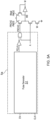
- FIG. 2 is a block diagram showing functional circuit blocks of a CIM cell 1, according to some embodiments.
- the CIM cell 1 includes a memory cell 2, calculation circuitry 3 that performs calculations based on an activation input A and the value W stored in the memory cell, and a precharge device 4 that precharges an output node of the calculation circuitry 3.
- Precharge logic 5 may control the precharge device 4 to precharge the output node 7 of the calculation circuitry 3 with a suitable timing.
- the precharge device 4 may be turned on (conductive) in response to the activation input A. After the precharge operation, the precharge device 4 is turned off (non-conductive).
- the calculation circuitry 3 is then ready to perform a calculation using the input A and the value W stored in the memory cell 2 when the CIM device 10 performs a compute operation.
- the CIM device 10 controls calculation circuitry 3 to perform a compute operation, the result of the calculation is provided to output node 7.
- the memory cell 2 may be any suitable type of memory cell, such as a static random access memory (SRAM) cell or a ternary content addressable memory (TCAM) cell, for example.
- FIG. 3 shows additional detail of one example of a CIM cell according to some embodiments.
- the calculation circuitry 3a is configured to perform multiplication of the activation input A and value W stored in the memory cell 2.
- the precharge logic 5 provides a signal PRCHG that controls precharge device 4a to precharge the output node 7a, also shown as node MB.
- the precharge device 4a may be a PMOS transistor that is controlled to perform the precharge operation in response to signal PRCHG having a low logic level. During the precharge operation the precharge device 4a is conductive, and connects output node 7a to the power rail 8.
- the CIM cell 1 may include an inverter 11 that inverts signal MB to produce signal M.
- Signal M may be provided to an adder tree to perform the addition portion of a multiply-accumulate calculation.
- A When a compute operation is performed the input A is multiplied by the value W stored in the memory cell 2.
- Values A and W may be digital values. If both A and W are logic high, the output node 7a is pulled down to ground (logic low). If either A or W or both are logic low, the output node 7a is not pulled down to ground and instead remains at the precharge voltage (logic high, in this example).
- the CIM cell 1 may include circuitry for maintaining MB at a high logic level when the precharge device is off and either A or W or both has a low logic level: in this example a weak PMOS device performs this function.
- FIG. 4A shows a circuit diagram of an embodiment of a CIM cell in which the gate of the precharge device 4a is connected to the activation input A.
- the precharge device 4a turns on and precharges node MB to the voltage of the power rail 8.
- FIG. 4C shows a timing diagram illustrating an activation input A having a low logic value causing MB to be precharged to a high logic value.
- FIG. 5A shows a diagram of another embodiment in which precharge logic 5a produces a precharge signal PRCHG in response to the activation input A.
- the precharge logic 5a includes a pulse generator 51 and other logic circuitry. With the precharge logic 5, the precharge operation can be initiated either by logic signal A having a low logic level or in response to a pulse signal PCLK produce in response to an enable signal EN.
- FIG. 5B shows a timing diagram illustrating the signals shown in FIG. 5A , with signal PEN being an internal signal of the pulse generator 51.
- the enable signal EN may transition from a low logic level to a high logic level when a compute operation is enabled in the CIM device 10.
- the pulse generator 51 may produce a pulse that causes an initial precharge operation to be performed.
- FIG. 6 illustrates that a CIM cell may have a plurality of memory cells storing respective weights W and a demultiplexer 12 that provides the input A to a transistor gate of a selected multiplier path corresponding to the selected weight W.
- the selection signal FA[u:0] is the selection signal of the demultiplexer, which determines which filter weight W is selected, and applies the activation signal A to the gate of the transistor RWL corresponding to the selected weight W.
- the precharge operation may be triggered in response to a change in the selection signal FA[u:0].
- the enable signal EN of the precharge logic 5a may be the selection signal FA[u:0].
- the precharge operation may be triggered in response to a change in any one of a plurality of signals, such as enable signal EN that switches to a logic high when a compute operation is enabled in the CIM device 10, and FA[u:0].
- the precharge logic 5 may activate the precharge operation in response to a change in any of such signals.
- FIG. 7 shows an example of such precharge logic as precharge logic 5b, which includes a pulse generator 71 configured to produce a pulse to initiate precharge in response to a change in either enable signal EN or selection signal FA[u:0].
- Coupled or “connected” is meant to refer to circuit elements, or signals, that are either directly linked to one another or through intermediate components.
- the terms “approximately”, “substantially,” and “about” may be used to mean within ⁇ 20% of a target value in some embodiments, within ⁇ 10% of a target value in some embodiments, within ⁇ 5% of a target value in some embodiments, and within ⁇ 2% of a target value in some embodiments.
- the terms “approximately” and “about” may include the target value.
Landscapes
- Engineering & Computer Science (AREA)
- Microelectronics & Electronic Packaging (AREA)
- Computer Hardware Design (AREA)
- Static Random-Access Memory (AREA)
- Logic Circuits (AREA)
- Dram (AREA)
Abstract
Description
- This application claims priority to and the benefit of
U.S. provisional application 63/322,251, filed March 22, 2022 - In conventional computing devices, a memory functional block is separate from a processor functional block. Data is fetched from the memory to perform operations in the processor functional block.
- Compute-in-memory (CIM) devices are devices in which operations may be performed in the memory. Such architectures may have the benefit of improved speed or lower power consumption. One example of an application for CIM devices is an implementing neural networks. Neural networks make extensive use of multiply accumulate operations, in which inputs are multiplied by filter weights and the products are summed. CIM devices may include hardware for performing the multiply and accumulate operations as well as memory cells for storing the filter weights.
- Some aspects relate to a method of operating a memory device, the method comprising precharging an output node of a cell of the memory device based on an activation input for the cell.
- In one arrangement, the precharging is performed through coupling the output node to a power rail using a transistor. The transistor might comprise a PMOS transistor.
- Preferably, the memory device is a compute-in-memory device and the cell comprises a memory cell and calculation circuitry configured to perform a calculation based on the activation input and a value stored in the memory cell. The calculation might be multiplication.
- In another arrangement, the cell includes a static random access memory (SRAM) cell and/or a ternary content addressable memory (TCAM) cell.
- Some aspects relate to a memory device comprising precharge circuitry configured to precharge an output node of a cell of the memory device based on an activation input for the cell.
- The foregoing summary is provided by way of illustration and is not intended to be limiting.
- The accompanying drawings are not intended to be drawn to scale. In the drawings, each identical or nearly identical component that is illustrated in various figures is represented by a like numeral. For purposes of clarity, not every component may be labeled in every drawing.
-
FIG. 1 illustrates a high-level block diagram of a compute-in-memory (CIM) device having an array of CIM cells arranged in rows and columns. -
FIG. 2 is a block diagram showing functional circuit blocks of a CIM cell and functional circuit blocks that provide signals to a CIM cell. -
FIG. 3 shows additional detail of one example of a CIM cell in which calculation circuitry is configured to perform multiplication of the input A and value W stored in a memory cell. -
FIG. 4A-4C show an embodiment for performing precharge based on an activation input. -
FIGS. 5A-5B show an embodiment for performing precharge based on an activation input. -
FIG. 6 illustrates that aCIM cell 1 may have a plurality of memory cells storing respective weights W and ademultiplexer 12 that provides the input A to a transistor gate of a selected multiplier path corresponding to the selected weight W. -
FIG. 7 shows an example of precharge logic including a pulse generator configured to produce a pulse to initiate precharge in response to a change in any one or more of a plurality of input signals. - The devices and techniques described herein allow for reducing the power consumption in a memory array due to precharge operations. The inventors have recognized and appreciated that conventional techniques for precharging an output node of a cell cause frequent switching of a precharge device connected to the output node, which may lead to high power consumption due to frequent charging and discharging of the gate capacitance of the precharge device. The power consumption can be reduced by switching the precharge device less frequently. In some embodiments, a precharge operation for a memory cell may be triggered by an activation input corresponding to the memory cell. Since the activation signal changes values relatively infrequently, the precharge device may be switched less frequently, and the power consumption caused by precharge may be reduced. Such techniques may be used in a compute-in-memory (CIM) device or other devices having a memory array.
-
FIG. 1 illustrates a high-level block diagram of a compute-in-memory (CIM)device 10 having an array ofCIM cells 1 arranged in rows and columns. TheCIM device 10 may have any number of rows and columns. EachCIM cell 1 has at least one memory cell and associated calculation circuitry, as discussed further below. The output node of the calculation circuitry needs to be precharged before performing a compute operation. -
FIG. 2 is a block diagram showing functional circuit blocks of aCIM cell 1, according to some embodiments. TheCIM cell 1 includes amemory cell 2,calculation circuitry 3 that performs calculations based on an activation input A and the value W stored in the memory cell, and aprecharge device 4 that precharges an output node of thecalculation circuitry 3.Precharge logic 5 may control theprecharge device 4 to precharge the output node 7 of thecalculation circuitry 3 with a suitable timing. In some embodiments, theprecharge device 4 may be turned on (conductive) in response to the activation input A. After the precharge operation, theprecharge device 4 is turned off (non-conductive). Thecalculation circuitry 3 is then ready to perform a calculation using the input A and the value W stored in thememory cell 2 when theCIM device 10 performs a compute operation. When theCIM device 10controls calculation circuitry 3 to perform a compute operation, the result of the calculation is provided to output node 7. Thememory cell 2 may be any suitable type of memory cell, such as a static random access memory (SRAM) cell or a ternary content addressable memory (TCAM) cell, for example. -
FIG. 3 shows additional detail of one example of a CIM cell according to some embodiments. In this example, thecalculation circuitry 3a is configured to perform multiplication of the activation input A and value W stored in thememory cell 2. Theprecharge logic 5 provides a signal PRCHG that controlsprecharge device 4a to precharge theoutput node 7a, also shown as node MB. Theprecharge device 4a may be a PMOS transistor that is controlled to perform the precharge operation in response to signal PRCHG having a low logic level. During the precharge operation theprecharge device 4a is conductive, and connectsoutput node 7a to thepower rail 8. TheCIM cell 1 may include aninverter 11 that inverts signal MB to produce signal M. Signal M may be provided to an adder tree to perform the addition portion of a multiply-accumulate calculation. When a compute operation is performed the input A is multiplied by the value W stored in thememory cell 2. Values A and W may be digital values. If both A and W are logic high, theoutput node 7a is pulled down to ground (logic low). If either A or W or both are logic low, theoutput node 7a is not pulled down to ground and instead remains at the precharge voltage (logic high, in this example). TheCIM cell 1 may include circuitry for maintaining MB at a high logic level when the precharge device is off and either A or W or both has a low logic level: in this example a weak PMOS device performs this function. -
FIG. 4A shows a circuit diagram of an embodiment of a CIM cell in which the gate of theprecharge device 4a is connected to the activation input A. As shown in the truth table ofFIG. 4B , when the activation input A has a logic value of zero theprecharge device 4a turns on and precharges node MB to the voltage of thepower rail 8.FIG. 4C shows a timing diagram illustrating an activation input A having a low logic value causing MB to be precharged to a high logic value. When a compute operation is performed and both A and W have high logic values, the node MB is pulled down to a low logic value. -
FIG. 5A shows a diagram of another embodiment in whichprecharge logic 5a produces a precharge signal PRCHG in response to the activation input A. Theprecharge logic 5a includes apulse generator 51 and other logic circuitry. With theprecharge logic 5, the precharge operation can be initiated either by logic signal A having a low logic level or in response to a pulse signal PCLK produce in response to an enable signal EN.FIG. 5B shows a timing diagram illustrating the signals shown inFIG. 5A , with signal PEN being an internal signal of thepulse generator 51. In some embodiments, the enable signal EN may transition from a low logic level to a high logic level when a compute operation is enabled in theCIM device 10. In response, thepulse generator 51 may produce a pulse that causes an initial precharge operation to be performed. -
FIG. 6 illustrates that a CIM cell may have a plurality of memory cells storing respective weights W and ademultiplexer 12 that provides the input A to a transistor gate of a selected multiplier path corresponding to the selected weight W. The selection signal FA[u:0] is the selection signal of the demultiplexer, which determines which filter weight W is selected, and applies the activation signal A to the gate of the transistor RWL corresponding to the selected weight W. - In some embodiments, the precharge operation may be triggered in response to a change in the selection signal FA[u:0]. To do so, the enable signal EN of the
precharge logic 5a may be the selection signal FA[u:0]. Alternatively or additionally, the precharge operation may be triggered in response to a change in any one of a plurality of signals, such as enable signal EN that switches to a logic high when a compute operation is enabled in theCIM device 10, and FA[u:0]. Theprecharge logic 5 may activate the precharge operation in response to a change in any of such signals.FIG. 7 shows an example of such precharge logic asprecharge logic 5b, which includes apulse generator 71 configured to produce a pulse to initiate precharge in response to a change in either enable signal EN or selection signal FA[u:0]. - Use of ordinal terms such as "first", "second", "third", etc., in the claims to modify a claim element does not by itself connote any priority, precedence, or order of one claim element over another or the temporal order in which acts of a method are performed, but are used merely as labels to distinguish one claim element having a certain name from another element having a same name (but for use of the ordinal term) to distinguish the claim elements.
- Also, the phraseology and terminology used herein is for the purpose of description and should not be regarded as limiting. The use of "including", "comprising", "having", "containing" or "involving" and variations thereof herein, is meant to encompass the items listed thereafter and equivalents thereof as well as additional items.
- The use of "coupled" or "connected" is meant to refer to circuit elements, or signals, that are either directly linked to one another or through intermediate components.
- The terms "approximately", "substantially," and "about" may be used to mean within ±20% of a target value in some embodiments, within ±10% of a target value in some embodiments, within ±5% of a target value in some embodiments, and within ±2% of a target value in some embodiments. The terms "approximately" and "about" may include the target value.
Claims (15)
- A method of operating a memory device, the method comprising:
precharging an output node of a cell of the memory device based on an activation input for the cell. - The method of claim 1, wherein the precharging is performed when the activation input has a first logic level.
- The method of claim 1 or 2, wherein the precharging is performed through coupling the output node to a power rail using a transistor.
- The method of any one of the preceding claims, wherein the memory device is a compute-in-memory device and the cell comprises a memory cell and calculation circuitry configured to perform a calculation based on the activation input and a value stored in the memory cell.
- The method of any one of the preceding claims, further comprising precharging the output node in response to an enable signal.
- The method of any one of the preceding claims, further comprising producing a pulse in response to a change in the enable signal.
- The method of any one of the preceding claims, wherein the cell stores a plurality of filter weights that are selectable based on a selection signal, and the method further comprises precharging the output node in response to a change in the selection signal.
- A memory device comprising:
precharge circuitry configured to precharge an output node of a cell of the memory device based on an activation input for the cell. - The memory device of claim 8, wherein the precharge circuitry precharges the output node when the activation input has a first logic level.
- The memory device of claim 8 or 9, wherein the precharge circuitry comprises a transistor configured to couple the output node to a power rail.
- The memory device of claim 8, 9 or 10, wherein the memory device is a compute-in-memory device and the cell comprises a memory cell and calculation circuitry configured to perform a calculation based on the activation input and a value stored in the memory cell.
- The memory device of any one of claims 8 to 11, wherein the precharge circuitry is configured to precharge the output node in response to an enable signal.
- The memory device of any one of claims 8 to 12, wherein the precharge circuitry comprises a pulse generator.
- The memory device of any one of claims 8 to 13, wherein the cell stores a plurality of filter weights that are selectable based on a selection signal, and the precharge circuitry is configured to precharge the output node in response to a change in the selection signal.
- The memory device of any one of claims 8 to 14, wherein the cell includes a static random access memory (SRAM) cell and/or a ternary content addressable memory (TCAM) cell.
Applications Claiming Priority (2)
| Application Number | Priority Date | Filing Date | Title |
|---|---|---|---|
| US202263322251P | 2022-03-22 | 2022-03-22 | |
| US18/175,511 US12327602B2 (en) | 2022-03-22 | 2023-02-27 | Reducing precharge power consumption in a memory array |
Publications (1)
| Publication Number | Publication Date |
|---|---|
| EP4250294A1 true EP4250294A1 (en) | 2023-09-27 |
Family
ID=85704673
Family Applications (1)
| Application Number | Title | Priority Date | Filing Date |
|---|---|---|---|
| EP23162966.8A Pending EP4250294A1 (en) | 2022-03-22 | 2023-03-20 | Reducing precharge power consumption in a memory array |
Country Status (3)
| Country | Link |
|---|---|
| US (1) | US12327602B2 (en) |
| EP (1) | EP4250294A1 (en) |
| TW (1) | TWI881308B (en) |
Families Citing this family (3)
| Publication number | Priority date | Publication date | Assignee | Title |
|---|---|---|---|---|
| US12327591B2 (en) | 2021-04-09 | 2025-06-10 | Mediatek Singapore Pte. Ltd. | Method and apparatus for performing a MAC operation in a memory array |
| US12106822B2 (en) | 2021-07-16 | 2024-10-01 | Mediatek Singapore Pte. Ltd. | Memory array with programmable number of filters |
| US20250111215A1 (en) * | 2023-09-28 | 2025-04-03 | Mediatek Inc. | Configurable computing-in-memory (cim) for power control |
Citations (3)
| Publication number | Priority date | Publication date | Assignee | Title |
|---|---|---|---|---|
| US20160225437A1 (en) * | 2015-02-04 | 2016-08-04 | Altera Corporation | Methods and apparatus for reducing power consumption in memory circuitry by controlling precharge duration |
| US20190103156A1 (en) * | 2018-09-28 | 2019-04-04 | Huseyin Ekin Sumbul | Full-rail digital read compute-in-memory circuit |
| US11018687B1 (en) * | 2020-05-13 | 2021-05-25 | Qualcomm Incorporated | Power-efficient compute-in-memory analog-to-digital converters |
Family Cites Families (23)
| Publication number | Priority date | Publication date | Assignee | Title |
|---|---|---|---|---|
| US6005813A (en) | 1997-11-12 | 1999-12-21 | Micron Technology, Inc. | Device and method for repairing a semiconductor memory |
| JP4624198B2 (en) | 2005-07-06 | 2011-02-02 | ルネサスエレクトロニクス株式会社 | Semiconductor memory device |
| US10832746B2 (en) | 2009-07-16 | 2020-11-10 | Gsi Technology Inc. | Non-volatile in-memory computing device |
| US9286980B2 (en) | 2014-01-10 | 2016-03-15 | Globalfoundries Inc. | Converting an XY TCAM to a value TCAM |
| US9564183B2 (en) | 2014-11-26 | 2017-02-07 | Invecas, Inc. | Sense amplifier having a timing circuit for a presearch and a main search |
| US9543015B1 (en) | 2015-09-22 | 2017-01-10 | Nxp Usa, Inc. | Memory array and coupled TCAM architecture for improved access time during search operation |
| TWI680409B (en) | 2017-07-08 | 2019-12-21 | 英屬開曼群島商意騰科技股份有限公司 | Method for matrix by vector multiplication for use in artificial neural network |
| US12131250B2 (en) | 2017-09-29 | 2024-10-29 | Intel Corporation | Inner product convolutional neural network accelerator |
| US10621489B2 (en) | 2018-03-30 | 2020-04-14 | International Business Machines Corporation | Massively parallel neural inference computing elements |
| US11049013B1 (en) | 2018-04-20 | 2021-06-29 | Perceive Corporation | Encoding of weight values stored on neural network inference circuit |
| US11669446B2 (en) | 2018-06-18 | 2023-06-06 | The Trustees Of Princeton University | Configurable in memory computing engine, platform, bit cells and layouts therefore |
| US10825510B2 (en) | 2019-02-09 | 2020-11-03 | Purdue Research Foundation | Multi-bit dot product engine |
| US11126402B2 (en) | 2019-03-21 | 2021-09-21 | Qualcomm Incorporated | Ternary computation memory systems and circuits employing binary bit cell-XNOR circuits particularly suited to deep neural network (DNN) computing |
| US10877731B1 (en) | 2019-06-18 | 2020-12-29 | Gsi Technology, Inc. | Processing array device that performs one cycle full adder operation and bit line read/write logic features |
| US10958272B2 (en) | 2019-06-18 | 2021-03-23 | Gsi Technology, Inc. | Computational memory cell and processing array device using complementary exclusive or memory cells |
| US20210012202A1 (en) | 2019-07-12 | 2021-01-14 | Facebook Technologies, Llc | Systems and methods for asymmetrical scaling factor support for negative and positive values |
| US11657238B2 (en) * | 2020-01-31 | 2023-05-23 | Qualcomm Incorporated | Low-power compute-in-memory bitcell |
| US11714570B2 (en) * | 2020-02-26 | 2023-08-01 | Taiwan Semiconductor Manufacturing Company, Ltd. | Computing-in-memory device and method |
| US11211115B2 (en) * | 2020-05-05 | 2021-12-28 | Ecole Polytechnique Federale De Lausanne (Epfl) | Associativity-agnostic in-cache computing memory architecture optimized for multiplication |
| US12002539B2 (en) * | 2020-08-04 | 2024-06-04 | National Tsing Hua University | Memory device and memory array structure using charge sharing for multi-bit convolutional neural network based computing-in-memory applications, and computing method thereof |
| US11538509B2 (en) * | 2021-03-17 | 2022-12-27 | Qualcomm Incorporated | Compute-in-memory with ternary activation |
| US12327591B2 (en) | 2021-04-09 | 2025-06-10 | Mediatek Singapore Pte. Ltd. | Method and apparatus for performing a MAC operation in a memory array |
| US12106822B2 (en) | 2021-07-16 | 2024-10-01 | Mediatek Singapore Pte. Ltd. | Memory array with programmable number of filters |
-
2023
- 2023-02-27 US US18/175,511 patent/US12327602B2/en active Active
- 2023-03-20 EP EP23162966.8A patent/EP4250294A1/en active Pending
- 2023-03-22 TW TW112110734A patent/TWI881308B/en active
Patent Citations (3)
| Publication number | Priority date | Publication date | Assignee | Title |
|---|---|---|---|---|
| US20160225437A1 (en) * | 2015-02-04 | 2016-08-04 | Altera Corporation | Methods and apparatus for reducing power consumption in memory circuitry by controlling precharge duration |
| US20190103156A1 (en) * | 2018-09-28 | 2019-04-04 | Huseyin Ekin Sumbul | Full-rail digital read compute-in-memory circuit |
| US11018687B1 (en) * | 2020-05-13 | 2021-05-25 | Qualcomm Incorporated | Power-efficient compute-in-memory analog-to-digital converters |
Also Published As
| Publication number | Publication date |
|---|---|
| TW202338807A (en) | 2023-10-01 |
| US12327602B2 (en) | 2025-06-10 |
| TWI881308B (en) | 2025-04-21 |
| US20230307017A1 (en) | 2023-09-28 |
Similar Documents
| Publication | Publication Date | Title |
|---|---|---|
| US12327602B2 (en) | Reducing precharge power consumption in a memory array | |
| TWI896590B (en) | Low-power compute-in-memory bitcell | |
| US11538509B2 (en) | Compute-in-memory with ternary activation | |
| US12217819B2 (en) | Computing device, memory controller, and method for performing an in-memory computation | |
| US11456030B2 (en) | Static random access memory SRAM unit and related apparatus | |
| US6243280B1 (en) | Selective match line pre-charging in a partitioned content addressable memory array | |
| US4021781A (en) | Virtual ground read-only-memory for electronic calculator or digital processor | |
| KR20220150895A (en) | Time-sharing compute-in-memory bitcell | |
| US12450472B2 (en) | Charge-pump-based current-mode neuron for machine learning | |
| Hussain et al. | Match-line division and control to reduce power dissipation in content addressable memory | |
| US4021656A (en) | Data input for electronic calculator or digital processor chip | |
| US4037090A (en) | Multiphase clocking for MOS | |
| EP0850480B1 (en) | Fast word line decoder for memory devices | |
| US3991305A (en) | Electronic calculator or digital processor chip with multiple code combinations of display and keyboard scan outputs | |
| US8526246B2 (en) | Write circuitry for hierarchical memory architectures | |
| US12354657B2 (en) | Reducing precharge current surge in digital compute in memory | |
| US5917771A (en) | Register bank bit lines | |
| CN113889158B (en) | Memory computing circuit, device and electronic equipment based on SRAM | |
| CN116798465A (en) | Methods of operating storage devices and storage devices | |
| US3989939A (en) | Electronic calculator or digital processor chip with combined functions for constant, keyboard and control bit | |
| US3991306A (en) | Electronic calculator or digital processor chip with separately controllable digit and segment outputs | |
| US5546024A (en) | Dynamic NOR decoder using current mode sensing techniques | |
| US11551748B2 (en) | System and method for recycling energy of static random-access memory (SRAM) write circuit | |
| US20260141949A1 (en) | Memory With Selective Negative Bit Line Boost | |
| US20230267993A1 (en) | Memory Write Assist with Reduced Switching Power |
Legal Events
| Date | Code | Title | Description |
|---|---|---|---|
| PUAI | Public reference made under article 153(3) epc to a published international application that has entered the european phase |
Free format text: ORIGINAL CODE: 0009012 |
|
| STAA | Information on the status of an ep patent application or granted ep patent |
Free format text: STATUS: THE APPLICATION HAS BEEN PUBLISHED |
|
| AK | Designated contracting states |
Kind code of ref document: A1 Designated state(s): AL AT BE BG CH CY CZ DE DK EE ES FI FR GB GR HR HU IE IS IT LI LT LU LV MC ME MK MT NL NO PL PT RO RS SE SI SK SM TR |
|
| STAA | Information on the status of an ep patent application or granted ep patent |
Free format text: STATUS: REQUEST FOR EXAMINATION WAS MADE |
|
| 17P | Request for examination filed |
Effective date: 20240327 |
|
| RBV | Designated contracting states (corrected) |
Designated state(s): AL AT BE BG CH CY CZ DE DK EE ES FI FR GB GR HR HU IE IS IT LI LT LU LV MC ME MK MT NL NO PL PT RO RS SE SI SK SM TR |
|
| STAA | Information on the status of an ep patent application or granted ep patent |
Free format text: STATUS: EXAMINATION IS IN PROGRESS |
|
| 17Q | First examination report despatched |
Effective date: 20250221 |