EP4249998A1 - Light control sheet and method for producing light control sheet - Google Patents
Light control sheet and method for producing light control sheet Download PDFInfo
- Publication number
- EP4249998A1 EP4249998A1 EP21894693.7A EP21894693A EP4249998A1 EP 4249998 A1 EP4249998 A1 EP 4249998A1 EP 21894693 A EP21894693 A EP 21894693A EP 4249998 A1 EP4249998 A1 EP 4249998A1
- Authority
- EP
- European Patent Office
- Prior art keywords
- light control
- layer
- groove
- transparent electrode
- transparent
- Prior art date
- Legal status (The legal status is an assumption and is not a legal conclusion. Google has not performed a legal analysis and makes no representation as to the accuracy of the status listed.)
- Granted
Links
Images



Classifications
-
- G—PHYSICS
- G02—OPTICS
- G02F—OPTICAL DEVICES OR ARRANGEMENTS FOR THE CONTROL OF LIGHT BY MODIFICATION OF THE OPTICAL PROPERTIES OF THE MEDIA OF THE ELEMENTS INVOLVED THEREIN; NON-LINEAR OPTICS; FREQUENCY-CHANGING OF LIGHT; OPTICAL LOGIC ELEMENTS; OPTICAL ANALOGUE/DIGITAL CONVERTERS
- G02F1/00—Devices or arrangements for the control of the intensity, colour, phase, polarisation or direction of light arriving from an independent light source, e.g. switching, gating or modulating; Non-linear optics
- G02F1/01—Devices or arrangements for the control of the intensity, colour, phase, polarisation or direction of light arriving from an independent light source, e.g. switching, gating or modulating; Non-linear optics for the control of the intensity, phase, polarisation or colour
- G02F1/13—Devices or arrangements for the control of the intensity, colour, phase, polarisation or direction of light arriving from an independent light source, e.g. switching, gating or modulating; Non-linear optics for the control of the intensity, phase, polarisation or colour based on liquid crystals, e.g. single liquid crystal display cells
- G02F1/133—Constructional arrangements; Operation of liquid crystal cells; Circuit arrangements
- G02F1/1333—Constructional arrangements; Manufacturing methods
- G02F1/1343—Electrodes
- G02F1/134309—Electrodes characterised by their geometrical arrangement
- G02F1/134327—Segmented, e.g. alpha numeric display
-
- G—PHYSICS
- G02—OPTICS
- G02F—OPTICAL DEVICES OR ARRANGEMENTS FOR THE CONTROL OF LIGHT BY MODIFICATION OF THE OPTICAL PROPERTIES OF THE MEDIA OF THE ELEMENTS INVOLVED THEREIN; NON-LINEAR OPTICS; FREQUENCY-CHANGING OF LIGHT; OPTICAL LOGIC ELEMENTS; OPTICAL ANALOGUE/DIGITAL CONVERTERS
- G02F1/00—Devices or arrangements for the control of the intensity, colour, phase, polarisation or direction of light arriving from an independent light source, e.g. switching, gating or modulating; Non-linear optics
- G02F1/01—Devices or arrangements for the control of the intensity, colour, phase, polarisation or direction of light arriving from an independent light source, e.g. switching, gating or modulating; Non-linear optics for the control of the intensity, phase, polarisation or colour
- G02F1/13—Devices or arrangements for the control of the intensity, colour, phase, polarisation or direction of light arriving from an independent light source, e.g. switching, gating or modulating; Non-linear optics for the control of the intensity, phase, polarisation or colour based on liquid crystals, e.g. single liquid crystal display cells
- G02F1/133—Constructional arrangements; Operation of liquid crystal cells; Circuit arrangements
- G02F1/1333—Constructional arrangements; Manufacturing methods
- G02F1/1343—Electrodes
- G02F1/13439—Electrodes characterised by their electrical, optical, physical properties; materials therefor; method of making
-
- G—PHYSICS
- G02—OPTICS
- G02F—OPTICAL DEVICES OR ARRANGEMENTS FOR THE CONTROL OF LIGHT BY MODIFICATION OF THE OPTICAL PROPERTIES OF THE MEDIA OF THE ELEMENTS INVOLVED THEREIN; NON-LINEAR OPTICS; FREQUENCY-CHANGING OF LIGHT; OPTICAL LOGIC ELEMENTS; OPTICAL ANALOGUE/DIGITAL CONVERTERS
- G02F1/00—Devices or arrangements for the control of the intensity, colour, phase, polarisation or direction of light arriving from an independent light source, e.g. switching, gating or modulating; Non-linear optics
- G02F1/01—Devices or arrangements for the control of the intensity, colour, phase, polarisation or direction of light arriving from an independent light source, e.g. switching, gating or modulating; Non-linear optics for the control of the intensity, phase, polarisation or colour
- G02F1/13—Devices or arrangements for the control of the intensity, colour, phase, polarisation or direction of light arriving from an independent light source, e.g. switching, gating or modulating; Non-linear optics for the control of the intensity, phase, polarisation or colour based on liquid crystals, e.g. single liquid crystal display cells
- G02F1/133—Constructional arrangements; Operation of liquid crystal cells; Circuit arrangements
- G02F1/1333—Constructional arrangements; Manufacturing methods
- G02F1/1339—Gaskets; Spacers; Sealing of cells
- G02F1/13396—Spacers having different sizes
-
- G—PHYSICS
- G02—OPTICS
- G02F—OPTICAL DEVICES OR ARRANGEMENTS FOR THE CONTROL OF LIGHT BY MODIFICATION OF THE OPTICAL PROPERTIES OF THE MEDIA OF THE ELEMENTS INVOLVED THEREIN; NON-LINEAR OPTICS; FREQUENCY-CHANGING OF LIGHT; OPTICAL LOGIC ELEMENTS; OPTICAL ANALOGUE/DIGITAL CONVERTERS
- G02F1/00—Devices or arrangements for the control of the intensity, colour, phase, polarisation or direction of light arriving from an independent light source, e.g. switching, gating or modulating; Non-linear optics
- G02F1/01—Devices or arrangements for the control of the intensity, colour, phase, polarisation or direction of light arriving from an independent light source, e.g. switching, gating or modulating; Non-linear optics for the control of the intensity, phase, polarisation or colour
- G02F1/13—Devices or arrangements for the control of the intensity, colour, phase, polarisation or direction of light arriving from an independent light source, e.g. switching, gating or modulating; Non-linear optics for the control of the intensity, phase, polarisation or colour based on liquid crystals, e.g. single liquid crystal display cells
- G02F1/1303—Apparatus specially adapted to the manufacture of LCDs
-
- G—PHYSICS
- G02—OPTICS
- G02F—OPTICAL DEVICES OR ARRANGEMENTS FOR THE CONTROL OF LIGHT BY MODIFICATION OF THE OPTICAL PROPERTIES OF THE MEDIA OF THE ELEMENTS INVOLVED THEREIN; NON-LINEAR OPTICS; FREQUENCY-CHANGING OF LIGHT; OPTICAL LOGIC ELEMENTS; OPTICAL ANALOGUE/DIGITAL CONVERTERS
- G02F1/00—Devices or arrangements for the control of the intensity, colour, phase, polarisation or direction of light arriving from an independent light source, e.g. switching, gating or modulating; Non-linear optics
- G02F1/01—Devices or arrangements for the control of the intensity, colour, phase, polarisation or direction of light arriving from an independent light source, e.g. switching, gating or modulating; Non-linear optics for the control of the intensity, phase, polarisation or colour
- G02F1/13—Devices or arrangements for the control of the intensity, colour, phase, polarisation or direction of light arriving from an independent light source, e.g. switching, gating or modulating; Non-linear optics for the control of the intensity, phase, polarisation or colour based on liquid crystals, e.g. single liquid crystal display cells
- G02F1/133—Constructional arrangements; Operation of liquid crystal cells; Circuit arrangements
- G02F1/1333—Constructional arrangements; Manufacturing methods
- G02F1/133305—Flexible substrates, e.g. plastics, organic film
-
- G—PHYSICS
- G02—OPTICS
- G02F—OPTICAL DEVICES OR ARRANGEMENTS FOR THE CONTROL OF LIGHT BY MODIFICATION OF THE OPTICAL PROPERTIES OF THE MEDIA OF THE ELEMENTS INVOLVED THEREIN; NON-LINEAR OPTICS; FREQUENCY-CHANGING OF LIGHT; OPTICAL LOGIC ELEMENTS; OPTICAL ANALOGUE/DIGITAL CONVERTERS
- G02F1/00—Devices or arrangements for the control of the intensity, colour, phase, polarisation or direction of light arriving from an independent light source, e.g. switching, gating or modulating; Non-linear optics
- G02F1/01—Devices or arrangements for the control of the intensity, colour, phase, polarisation or direction of light arriving from an independent light source, e.g. switching, gating or modulating; Non-linear optics for the control of the intensity, phase, polarisation or colour
- G02F1/13—Devices or arrangements for the control of the intensity, colour, phase, polarisation or direction of light arriving from an independent light source, e.g. switching, gating or modulating; Non-linear optics for the control of the intensity, phase, polarisation or colour based on liquid crystals, e.g. single liquid crystal display cells
- G02F1/133—Constructional arrangements; Operation of liquid crystal cells; Circuit arrangements
- G02F1/1333—Constructional arrangements; Manufacturing methods
- G02F1/1339—Gaskets; Spacers; Sealing of cells
- G02F1/13392—Gaskets; Spacers; Sealing of cells spacers dispersed on the cell substrate, e.g. spherical particles, microfibres
-
- G—PHYSICS
- G02—OPTICS
- G02F—OPTICAL DEVICES OR ARRANGEMENTS FOR THE CONTROL OF LIGHT BY MODIFICATION OF THE OPTICAL PROPERTIES OF THE MEDIA OF THE ELEMENTS INVOLVED THEREIN; NON-LINEAR OPTICS; FREQUENCY-CHANGING OF LIGHT; OPTICAL LOGIC ELEMENTS; OPTICAL ANALOGUE/DIGITAL CONVERTERS
- G02F1/00—Devices or arrangements for the control of the intensity, colour, phase, polarisation or direction of light arriving from an independent light source, e.g. switching, gating or modulating; Non-linear optics
- G02F1/01—Devices or arrangements for the control of the intensity, colour, phase, polarisation or direction of light arriving from an independent light source, e.g. switching, gating or modulating; Non-linear optics for the control of the intensity, phase, polarisation or colour
- G02F1/13—Devices or arrangements for the control of the intensity, colour, phase, polarisation or direction of light arriving from an independent light source, e.g. switching, gating or modulating; Non-linear optics for the control of the intensity, phase, polarisation or colour based on liquid crystals, e.g. single liquid crystal display cells
- G02F1/133—Constructional arrangements; Operation of liquid crystal cells; Circuit arrangements
- G02F1/1333—Constructional arrangements; Manufacturing methods
- G02F1/1343—Electrodes
- G02F1/134309—Electrodes characterised by their geometrical arrangement
-
- G—PHYSICS
- G02—OPTICS
- G02F—OPTICAL DEVICES OR ARRANGEMENTS FOR THE CONTROL OF LIGHT BY MODIFICATION OF THE OPTICAL PROPERTIES OF THE MEDIA OF THE ELEMENTS INVOLVED THEREIN; NON-LINEAR OPTICS; FREQUENCY-CHANGING OF LIGHT; OPTICAL LOGIC ELEMENTS; OPTICAL ANALOGUE/DIGITAL CONVERTERS
- G02F2202/00—Materials and properties
- G02F2202/28—Adhesive materials or arrangements
Definitions
- the present disclosure relates to a light control sheet having a variable light transmittance, and a method of producing the light control sheet.
- a light control sheet includes a light control layer containing a liquid crystal composition, and a pair of transparent electrode layers sandwiching the light control layer.
- a drive voltage is applied between the pair of transparent electrode layers.
- the alignment of liquid crystal molecules of the liquid crystal composition changes according to a potential difference between the transparent electrode layers, leading to a change in light transmittance of the light control sheet.
- the light control sheet is colorless and transparent, and has a high light transmittance.
- the major axes of the liquid crystal molecules intersect the thickness direction of the light control layer, light is scattered in the light control layer, and the light transmittance of the light control sheet is low (see, for example, Patent Literature 1).
- Light control sheets are adhered to members for partitioning a space, for example, construction materials such as window glasses or partitions of buildings, or window glasses of vehicles, and are used as a part of such members.
- members for partitioning a space for example, construction materials such as window glasses or partitions of buildings, or window glasses of vehicles, and are used as a part of such members.
- Improvement in the designability of light control sheets can significantly increase the applicability of light control sheets, and create a new demand for a space to be light controlled.
- light control sheets having higher designability are required to be developed.
- the light control sheet includes a first transparent electrode layer, a second transparent electrode layer, a light control layer that is located between the first transparent electrode layer and the second transparent electrode layer, a first transparent support layer that is located on a side of the first transparent electrode layer facing away from the light control layer and has a support surface that supports the first transparent electrode layer, and a second transparent support layer that is located on a side of the second transparent electrode layer facing away from the light control layer, wherein the first transparent electrode layer includes a first electrode element and a second electrode element, the first electrode element and the second electrode element are separate layered members arranged along the support surface, and are electrically insulated from each other by a groove extending along the support surface, a depth direction of the groove is a thickness direction of the first transparent electrode layer, and the groove has a depth that allows the groove to pass through the first transparent electrode layer but not to pass through the first transparent support layer.
- the method of producing a light control sheet includes preparing a laminate including a first transparent support layer and a first transparent electrode layer supported by the first transparent support layer and making a slit in the transparent electrode layer and the transparent support layer from a side where the first transparent electrode layer is located to form a groove in order to form a first electrode element and a second electrode element formed by the groove in the first transparent electrode layer, the groove having a depth that allows the groove to pass through the first transparent electrode layer but not to pass through the first transparent support layer, and forming a light control layer between the laminate having the groove and a laminate including a second transparent support layer and a second transparent electrode layer supported by the second transparent support layer.
- a light control sheet 10 of the present embodiment is a normal-type light control sheet in which when no voltage signal is applied to the light control sheet 10, incident light in a region to be driven is scattered to reduce the translucency of the light control sheet 10 and when a voltage signal is applied to the light control sheet 10, the translucency of the light control sheet 10 is increased.
- the light control sheet 10 has a first surface 11F, and a second surface 11R opposite to the first surface 11F.
- the light control sheet 10 has a drive region 20 and a non-driven region 21.
- the drive region 20 is a region in which a driving electrode element 30 is located.
- the driving electrode element 30 is an electrode element to which a voltage signal is applied when the light control sheet 10 is driven.
- the light transmittance of the drive region 20 changes according to the application state of a voltage signal to the driving electrode element 30.
- the driving electrode element 30 is an example of a first electrode element.
- the non-driven region 21 includes a floating region 22, and a boundary region 23 that surrounds the floating region 22.
- the floating region 22 is a region in which a floating electrode element 31 is located.
- the floating electrode element 31 is an electrode element to which no voltage signal is applied when the light control sheet 10 is driven.
- the floating electrode element 31 is an example of a second electrode element.
- the boundary region 23 is located between the drive region 20 and the floating region 22, and has a closed frame shape surrounding the floating region 22. No electrode element is located in the boundary region 23.
- the light transmittance of the non-driven region 21 does not change in response to the light control sheet 10 being driven or not driven.
- the non-driven region 21 causes the light control sheet 10 to display a design.
- the design is, for example, a character, a number, a symbol, a figure, a pattern, a patterned design, or the like, or a combination thereof.
- the light control sheet 10 shown in Fig. 1 is configured to display a single star-shaped figure; however, the light control sheet 10 may have a plurality of non-driven regions 21 separated from each other. That is, the light control sheet 10 may have a plurality of boundary regions 23 each of which forms a closed region.
- connection region 24 is a region for applying a voltage signal to the drive region 20, and external wires 25 are connected to the connection region 24.
- the connection region 24 and the drive region 20 are adjacent to each other.
- the position in the light control sheet 10 where the connection region 24 is to be provided is not particularly limited.
- the connection region 24 is located, for example, in a corner portion of the light control sheet 10.
- Fig. 2 is a cross-sectional view taken along line II-II in Fig. 1 . That is, Fig. 2 shows a cross-sectional structure of the light control sheet 10 in the drive region 20 and the connection region 24.
- the thickness ratio of the layers in Fig. 2 is shown for convenience of description, and the thickness ratio of the layers is not limited to the thickness ratio shown in Fig. 2 .
- the light control sheet 10 includes a light control layer 11, a first transparent electrode layer 12A, a second transparent electrode layer 12B, a first transparent support layer 13A, and a second transparent support layer 13B.
- the light control layer 11 is sandwiched between the first transparent electrode layer 12A and the second transparent electrode layer 12B.
- the first transparent support layer 13A supports the first transparent electrode layer 12A by a support surface 130 on the side of the first transparent electrode layer 12A facing away from the light control layer 11.
- the second transparent support layer 13B supports the second transparent electrode layer 12B on the side of the second transparent electrode layer 12B facing away from the light control layer 11.
- the light control layer 11 may have a single-layer structure or a multilayer structure.
- the light control layer 11 having a multilayer structure may include a functional layer having a light control function, a thin layer for improving adhesion between the functional layer and the first transparent electrode layer 12A, and a thin layer for improving adhesion between the functional layer and the second transparent electrode layer 12B.
- the light control sheet 10 further includes a protective layer 44.
- the protective layer 44 is located on the side of the first transparent support layer 13A facing away from the first transparent electrode layer 12A.
- the protective layer 44 is fixed to the first transparent support layer 13A via an adhesive layer (not shown).
- the first surface 11F of the light control sheet 10 is a surface opposite to a surface of the protective layer 44 facing the first transparent support layer 13A.
- the second surface 11R of the light control sheet 10 is a surface opposite to a surface of the second transparent support layer 13B facing the second transparent electrode layer 12B.
- the second surface 11R is adhered to a transparent plate made of glass, resin, or the like via an adhesive layer (not shown).
- the transparent plate is, for example, a window glass of various buildings such as houses, stores, stations, and airports, a partition in offices, a display window in stores, or a window glass or a windshield of moving objects such as vehicles and aircraft.
- the transparent plate may have a flat surface or a curved surface.
- connection region 24 includes a first connection region 24A that is connected to an external wire 25 for applying a voltage signal to the first transparent electrode layer 12A, and a second connection region 24B that is connected to an external wire 25 for applying a voltage signal to the second transparent electrode layer 12B.
- the first connection region 24A is a region that does not include the light control layer 11, the second transparent electrode layer 12B, or the second transparent support layer 13B and in which the first transparent electrode layer 12A is exposed.
- a first terminal portion 50A is connected to the first transparent electrode layer 12A exposed in the first connection region 24A. That is, the driving electrode element 30 extends from the drive region 20 to the first connection region 24A, and the first terminal portion 50A is connected to the driving electrode element 30 in the first connection region 24A.
- the second connection region 24B is a region that does not include the light control layer 11, the first transparent electrode layer 12A, the first transparent support layer 13A, or the protective layer 44 and in which the second transparent electrode layer 12B is exposed.
- a second terminal portion 50B is connected to the second transparent electrode layer 12B exposed in the second connection region 24B. That is, the driving electrode element 30 extends from the drive region 20 to the second connection region 24B, and the second terminal portion 50B is connected to the driving electrode element 30 in the second connection region 24B.
- One of the external wires 25 extends from the first terminal portion 50A and the other external wire 25 extends from the second terminal portion 50B, and the external wires 25 are connected to the control unit 50.
- the control unit 50 applies a voltage signal to the driving electrode element 30 of the first transparent electrode layer 12A through the first terminal portion 50A, and applies a voltage signal to the second transparent electrode layer 12B through the second terminal portion 50B.
- the control unit 50 controls a potential difference between the first transparent electrode layer 12A and the second transparent electrode layer 12B in the drive region 20.
- the second transparent electrode layer 12B is controlled to have, for example, a ground potential.
- the light control sheet 10 and the control unit 50 constitute a light control device.
- the light control layer 11 includes a transparent polymer layer and a liquid crystal composition.
- the transparent polymer layer has voids in which the liquid crystal composition is filled.
- the liquid crystal composition is filled in the voids of the transparent polymer layer.
- the liquid crystal composition contains liquid crystal molecules.
- the liquid crystal composition may be made of a known material.
- the liquid crystal molecules are, for example, selected from the group consisting of those based on Schiff bases, azo types, azoxy types, biphenyls, terphenyls, benzoic acid esters, tolans, pyrimidines, cyclohexanecarboxylic acid esters, phenylcyclohexanes, and dioxanes.
- the light control layer 11 having a single-layer structure is composed of only a functional layer including a transparent polymer layer and a liquid crystal composition.
- the liquid crystal composition is held in one of a polymer network type, a polymer dispersion type, and a capsule type.
- the polymer network type has a three-dimensional mesh transparent polymer network. Voids of the mesh communicate with each other, and a liquid crystal composition is held in the voids.
- the polymer network is an example of a transparent polymer layer.
- the polymer dispersion type has a large number of isolated voids in a transparent polymer layer, and holds a liquid crystal composition in the voids dispersed in the polymer layer.
- the capsule type holds an encapsulated liquid crystal composition in a transparent polymer layer.
- the liquid crystal composition may contain a monomer for forming a transparent polymer layer, dichroic dye, and the like, in addition to the liquid crystal molecules described above.
- the first transparent electrode layer 12A and the second transparent electrode layer 12B are each conductive and transparent to light in the visible region.
- the first transparent electrode layer 12A and the second transparent electrode layer 12B may be made of a known material. Examples of the material for forming the first transparent electrode layer 12A and the second transparent electrode layer 12B include indium tin oxide, fluorine-doped tin oxide, tin oxide, zinc oxide, carbon nanotubes, and poly(3,4-ethylenedioxythiophene).
- the first transparent support layer 13A and the second transparent support layer 13B are each a substrate transparent to light in the visible region.
- the first transparent support layer 13A and the second transparent support layer 13B may be made of a known material.
- the material for forming the first transparent support layer 13A and the second transparent support layer 13B may be, for example, a synthetic resin or an inorganic compound.
- the synthetic resin include polyester, polyacrylate, polycarbonate, and polyolefin.
- Examples of the polyester include polyethylene terephthalate and polyethylene naphthalate.
- the polyacrylate may be, for example, polymethyl methacrylate or the like.
- the inorganic compound include silicon dioxide, silicon oxynitride, and silicon nitride.
- the first terminal portion 50A and the second terminal portion 50B each include, for example, a conductive adhesive layer and a circuit board.
- the conductive adhesive layer is composed of, for example, an anisotropic conductive film (ACF), an anisotropic conductive paste (ACP), an isotropic conductive film (ICF), an isotropic conductive paste (ICP), or the like.
- the circuit board may be, for example, a flexible printed circuit (FPC).
- first terminal portion 50A and the second terminal portion 50B each may have a structure in which a conductive material such as a conductive tape is joined to the external wire 25 by soldering or the like.
- a change in the voltage generated between the two transparent electrode layers 12A and 12B causes a change in the alignment of the liquid crystal molecules in the light control layer 11.
- the change in the alignment of the liquid crystal molecules leads to a change in the degree of scattering, degree of absorption, and degree of transmission of visible light incident on the light control layer 11.
- the major axes of the liquid crystal molecules are oriented in random directions. This leads to a high degree of scattering of light incident on the light control layer 11, causing the drive region 20 to appear turbid. That is, the drive region 20 is opaque when no voltage signal is applied to the light control layer 11.
- the liquid crystal molecules are aligned, and the major axes of the liquid crystal molecules are aligned in the direction of an electric field between the transparent electrode layers 12A and 12B.
- the drive region 20 is transparent.
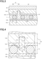
- Fig. 3 is a cross-sectional view taken along line III-III in Fig. 1 , and shows a cross-sectional structure of the light control sheet 10 in the boundary region 23 and in the drive region 20 and the floating region 22 between which the boundary region 23 is located.
- the light control layer 11 includes a plurality of spacers 15.
- the spacers 15 maintain an approximately constant distance between the first transparent electrode layer 12A and the second transparent electrode layer 12B.
- the driving electrode element 30 is located in the drive region 20, and the floating electrode element 31 is located in the floating region 22.
- the driving electrode element 30 and the floating electrode element 31 are separate layered members arranged along the support surface 130 of the first transparent support layer 13A.
- the driving electrode element 30 and the floating electrode element 31 are separated from each other by a groove 120.
- the depth direction of the groove 120 is the thickness direction of the first transparent electrode layer 12A.
- the groove 120 has an opening 122 in a portion of the first transparent electrode layer 12A facing the light control layer 11, and passes through the first transparent electrode layer 12A and extends halfway in the thickness direction of the first transparent support layer 13A.
- the driving electrode element 30 and the floating electrode element 31 are insulated from each other by being separated by the groove 120.
- the boundary region 23 is a region in which the groove 120 is located.
- Fig. 4 is an enlarged view of a cross-sectional structure of the groove 120 and a portion of the light control sheet 10 around the groove 120 in Fig. 3 .
- the thickness T2 of the first transparent electrode layer 12A is several tens of nanometers.
- the light control layer 11 has a thickness of 0.5 ⁇ m or more and 460 ⁇ m or less.
- the thickness of the entire light control sheet 10 is 45 ⁇ m or more and 500 ⁇ m or less.
- the thickness of the second transparent support layer 13B may be the same as or different from the thickness of the first transparent support layer 13A.
- the thickness of the second transparent electrode layer 12B may be the same as or different from the thickness of the first transparent electrode layer 12A.
- the depth of the groove 120 satisfies "T2 ⁇ D1 ⁇ T3", where "D1" is the depth of the groove 120.
- the groove 120 has a depth that allows the groove 120 to pass through the first transparent electrode layer 12A but not to pass through the first transparent support layer 13A.
- the groove 120 has a width W1 smaller than a diameter ⁇ 1 of the spacer 15 (width W1 ⁇ diameter ⁇ 1).
- the diameter ⁇ 1 of the spacer 15 is the diameter of the spacer 15 having the smallest particle diameter.
- the diameter ⁇ 1 of the spacer 15 is larger than the width W1 of the groove 120; thus, the spacer 15 is less likely to enter the groove 120.
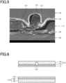
- Fig. 5 is an SEM photograph of a cross-sectional structure including the groove 120.
- the groove 120 shown at the center of the photograph is opened on the light control layer 11 side; thus, the groove 120 is filled with a light control material 110 composed of the transparent polymer layer and the liquid crystal composition of the light control layer 11. If the light control material 110 is not filled in the groove 120, light that is transmitted through the first transparent support layer 13A and is incident on the inside of the groove 120 is reflected by a side surface of the groove 120. In this case, the groove 120 is conspicuous when viewed from the outside of the light control sheet 10.
- the groove 120 is less likely to be visually recognized when viewed from the outside of the light control sheet 10. This is because in such a case, the side surface of the groove 120 has a low reflectance due to the refractive index of the material constituting the first transparent support layer 13A being closer to the refractive index of the light control material 110 than to the refractive index of air. Even if a small void 121 (see Fig. 4 ) remains in the groove 120, when most part of the groove 120 is filled with the light control material 110, the groove 120 is less conspicuous. In order to obtain an effect in which the groove 120 is less likely to be visually recognized from the outside, the filling ratio of the light control material 110 in the groove 120 may preferably be 80% or more.
- the width W1 of the groove 120 is smaller than the diameter ⁇ 1 of the spacers 15; thus, it is possible to prevent the spacers 15 from entering the groove 120 and interfere with filling of the groove 120 with the light control material 110.
- the thickness of the light control layer 11 is 0.5 ⁇ m or more; thus, the light control material 110 is more likely to be filled in the groove 120 at a filling ratio of 80% or more.
- the light control layer 11 having a large thickness ensures a sufficient amount of light control material 110 around the opening 122. Therefore, the light control material 110 is more likely to be filled in the groove 120 when a predetermined pressure is applied to the light control layer 11 sandwiched between the first transparent electrode layer 12A and the second transparent electrode layer 12B.
- the first transparent electrode layer 12A has a burr 123 formed around the opening 122 of the groove 120.
- the burr 123 is generated when the groove 120 is formed in the first transparent electrode layer 12A, and the burr 123 protrudes from the periphery of the opening 122 toward the light control layer 11.
- the burr 123 is adjusted to have a height H1 (see Fig. 4 ) smaller than a thickness T4 (see Fig. 4 ) of the light control layer 11 (H1 ⁇ T4).
- the first transparent electrode layer 12A is in contact with the second transparent electrode layer 12B via the light control layer 11, causing a short circuit between the first transparent electrode layer 12A and the second transparent electrode layer 12B.
- the height H1 of the burr 123 may be 0.8 times or less of the thickness T4 of the light control layer 11. In such a case, even when, for example, the light control sheet 10 is adhered to a curved surface or the light control sheet 10 is unintentionally pressed, and the distance between the first transparent electrode layer 12A and the second transparent electrode layer 12B is reduced, it is possible to sufficiently prevent a short circuit between the first transparent electrode layer 12A and the second transparent electrode layer 12B.
- the depth D1 of the groove 120 is the length of the groove 120 extending in the thickness direction of the first transparent electrode layer 12A from a surface of the first transparent electrode layer 12A on the light control layer 11 side, and does not include the height of the burr 123.
- a film 51A including the first transparent electrode layer 12A and the first transparent support layer 13A, and a film 51B including the second transparent electrode layer 12B and the second transparent support layer 13B are prepared.
- a cutting plotter is brought into contact with the first transparent electrode layer 12A of the film 51A including the first transparent electrode layer 12A and the first transparent support layer 13A to form the groove 120.
- a control device connected to the cutting plotter causes the cutting plotter to form the groove 120 along a design input in advance.
- a device other than the cutting plotter may be used to form the groove 120.
- cutting tools other than the cutting plotter, or a laser cutting device may be used to form the groove 120 in the first transparent electrode layer 12A.
- the laser cutting device may be, for example, a laser cutter including a CO 2 laser.
- a liquid material including the spacers 15 containing divinylbenzene or the like as a main material and a dispersion medium for dispersing the spacers 15 is applied to a surface of the film 51A on the first transparent electrode layer 12A side and a surface of the film S 1B on the second transparent electrode layer 12B side. Furthermore, the films on which the spacers 15 are scattered are heated to remove the dispersion medium. At this time, the spacers 15 may be scattered on only one of the films.
- a light control material containing a transparent polymer material and a liquid crystal composition is applied to the first transparent electrode layer 12A of the film 51A having the groove 120 and to the second transparent electrode layer 12B of the film S 1B having no groove 120.
- the groove 120 may not be filled with the light control material.
- the films 51A and 51B are irradiated with ultraviolet light under a nitrogen atmosphere to form light control layers 11A and 11B, respectively.
- the pair of films obtained in this manner are laminated and attached together while a predetermined amount of pressure is applied to the films.
- the groove 120 is filled with the light control material.
- the light control sheet 10 may be formed either by a roll-to-roll method or a single-sheet production process.
- a film transferred from a roll on the upstream side is subjected to various steps and then wound around a roll on the downstream side.
- a film cut into a predetermined size is subjected to various steps.
- the step of forming the groove 120 is performed before the film composed of the first transparent electrode layer 12A and the first transparent support layer 13A and the film composed of the second transparent electrode layer 12B and the second transparent support layer 13B are attached together via the light control layer 11.
- a slit is made in a corner portion of the second surface 11R of the light control sheet 10 having a predetermined size, and the second transparent support layer 13B and the second transparent electrode layer 12B in the corner portion are peeled off. Furthermore, the light control layer 11 in the corner portion is removed to expose the first transparent electrode layer 12A to form the connection region 24. Similarly, the connection region 24 is formed in a corner portion of the first surface 11F. Then, the first terminal portion 50A and the second terminal portion 50B are formed, and the external wires 25 are connected to the connection region 24. Furthermore, the connection region 24 is sealed with an epoxy resin or the like. The step of attaching the protective layer 44 to the first transparent support layer 13A may be performed after the pair of films are attached together.
- making a slit in the first transparent electrode layer 12A and the first transparent support layer 13A to form the groove 120 enables simpler formation of the groove 120 compared with, for example, a production method including steps such as formation of a resist mask required for patterning, exposure, development, etching, removal of the resist mask, and washing.
- Fig. 7 schematically shows the degree of transparency of the light control sheet 10 when the light control sheet 10 is not driven, that is, when no voltage signal is applied to the first transparent electrode layer 12A or the second transparent electrode layer 12B.
- the drive region 20 and the non-driven region 21 are both opaque. Therefore, the entire surface of the light control sheet 10 appears, for example, whitish and turbid, and an image of the character, pattern, or the like composed of the non-driven region 21 is not visually recognized.
- the groove 120 has a depth that allows the groove 120 to pass through the first transparent electrode layer 12A but not to pass through the first transparent support layer 13A; thus, the groove 120 is not conspicuous when viewed from either the first surface 11F or the second surface 11R of the light control sheet 10.
- the groove 120 is even less likely to be visually recognized. This allows the light control sheet 10 to have a better aesthetic appearance when the design is displayed.
- the drive region 20 is transparent and the non-driven region 21 is opaque. Therefore, only the non-driven region 21 appears, for example, whitish and turbid, and an image of the design such as a character or pattern composed of the non-driven region 21 can be visually recognized.
- the surface of the light control sheet 10 has the regions different in light transmittance to each other, and the difference in light transmittance between the regions is shown only when the light control sheet 10 is driven. Therefore, when the light control sheet 10 is driven, an image of the character, pattern, or the like composed of the non-driven region 21 is visually recognized, enabling decoration of a space in which the light control sheet 10 is provided. Furthermore, by switching the light control sheet 10 between the driven state and the non-driven state, the light control sheet 10 can be switched between the state in which the image is displayed and the state in which the image is not displayed, enabling a dynamic change in the decoration state of the space. This allows the light control sheet 10 to have higher designability.
- Fig. 9 shows an example of the light control sheet 10 as a reverse-type light control sheet.
- the light control layer 11 of the light control sheet 10 as a reverse-type light control sheet has a multilayer structure, and includes a functional layer 111 including a transparent polymer layer and a liquid crystal composition, a first alignment layer 112, and a second alignment layer 113.
- the first alignment layer 112 and the second alignment layer 113 constitute the light control layer 11.
- the first alignment layer 112 is located between the light control layer 11 and the first transparent electrode layer 12A, and is in contact with these layers.
- the second alignment layer 113 is located between the light control layer 11 and the second transparent electrode layer 12B, and is in contact with these layers.
- the first alignment layer 112 and the second alignment layer 113 are each, for example, a vertical alignment film or a horizontal alignment film.
- a vertical alignment film causes the major axes of liquid crystal molecules to be aligned in the thickness direction of the light control layer 11.
- a horizontal alignment film causes the major axes of liquid crystal molecules to be aligned in a direction substantially perpendicular to the thickness direction of the light control layer 11.
- the material for forming each of the first alignment layer 112 and the second alignment layer 113 is an organic compound, an inorganic compound, or a mixture thereof.
- the organic compound include polyimide, polyamide, polyvinyl alcohol, and cyanide compounds.
- the inorganic compound include silicon oxide and zirconium oxide.
- the material for forming the first alignment layer 112 and the second alignment layer 113 may be silicone. Silicone is a compound having an inorganic portion and an organic portion.
- the groove 120 has the opening 122 in a portion of the first alignment layer 112 facing the light control layer 11, and passes through the first alignment layer 112 and the first transparent electrode layer 12A but does not pass through the first transparent electrode layer 12A. That is, the depth of the groove 120 is smaller than the sum of the thickness of the first alignment layer 112, the thickness of the first transparent electrode layer 1A, and the thickness of the first transparent support layer 13A.
- the groove 120 is filled with a part of the light control layer 11.
- the drive region 20 of the light control sheet 10 including the first alignment layer 112 and the second alignment layer 113, when no voltage signal is applied to the transparent electrode layer 12A or 12B, the major axes of the liquid crystal molecules are aligned in the thickness direction of the light control layer 11. Thus, the drive region 20 is transparent.
- the drive region 20 when a voltage signal is applied to the transparent electrode layers 12A and 12B, the major axes of the liquid crystal molecules are aligned in a direction intersecting the thickness direction of the light control layer 11. Thus, the drive region 20 appears turbid and opaque.
- the major axes of the liquid crystal molecules are constantly aligned in the thickness direction of the light control layer 11; thus, the non-driven region 21 is constantly transparent.
- the drive region 20 and the non-driven region 21 are both transparent, and an image of the character, pattern, or the like composed of the non-driven region 21 is not visually recognized.
- the drive region 20 is opaque and the non-driven region 21 is transparent; thus, an image of the character, pattern, or the like composed of the non-driven region 21 can be visually recognized.
- the surface of the light control sheet 10 has the regions different in light transmittance to each other, and the difference in light transmittance between the regions is shown only when the light control sheet 10 is driven. Accordingly, this allows the light control sheet 10 to have higher designability.
- the groove 120 passes through the first alignment layer 112; however, the first alignment layer 112 may be formed after the groove 120 is formed in a laminate composed of the first transparent electrode layer 12A and the first transparent support layer 13A. In such a case, the first alignment layer 112 is formed along the bottom surface and side surface of the groove 120. This also enables the groove 120 to be less conspicuous when viewed externally.
- a first region in which the first electrode element is located is switched between the transparent state and the opaque state by switching the application state of a voltage signal to the first electrode element.
- a second region in which the second electrode element is located is switched between the transparent state and the opaque state independently from the first region by switching the application state of a voltage signal to the second electrode element.
- the first region is switched between the transparent state and the opaque state by switching the application state of a voltage signal to the first electrode element
- the second region is switched between the translucent state and the opaque state by switching the application state of a voltage signal to the second electrode element.
- the first region is transparent
- the second region is controlled to be translucent.
Landscapes
- Physics & Mathematics (AREA)
- Nonlinear Science (AREA)
- Mathematical Physics (AREA)
- Chemical & Material Sciences (AREA)
- Crystallography & Structural Chemistry (AREA)
- General Physics & Mathematics (AREA)
- Optics & Photonics (AREA)
- Liquid Crystal (AREA)
- Geometry (AREA)
Abstract
Description
- The present disclosure relates to a light control sheet having a variable light transmittance, and a method of producing the light control sheet.
- A light control sheet includes a light control layer containing a liquid crystal composition, and a pair of transparent electrode layers sandwiching the light control layer. A drive voltage is applied between the pair of transparent electrode layers. The alignment of liquid crystal molecules of the liquid crystal composition changes according to a potential difference between the transparent electrode layers, leading to a change in light transmittance of the light control sheet. For example, when the major axes of the liquid crystal molecules are aligned in the thickness direction of the light control layer, the light control sheet is colorless and transparent, and has a high light transmittance. When the major axes of the liquid crystal molecules intersect the thickness direction of the light control layer, light is scattered in the light control layer, and the light transmittance of the light control sheet is low (see, for example, Patent Literature 1).
- [PTL 1]
JP 2018-45135 A - Light control sheets are adhered to members for partitioning a space, for example, construction materials such as window glasses or partitions of buildings, or window glasses of vehicles, and are used as a part of such members. In recent years, in order to improve the added value of light control sheets, the designability of light control sheets has been attracting attention. Improvement in the designability of light control sheets can significantly increase the applicability of light control sheets, and create a new demand for a space to be light controlled. Thus, light control sheets having higher designability are required to be developed.
- An aspect of the present disclosure provides a light control sheet. The light control sheet includes a first transparent electrode layer, a second transparent electrode layer, a light control layer that is located between the first transparent electrode layer and the second transparent electrode layer, a first transparent support layer that is located on a side of the first transparent electrode layer facing away from the light control layer and has a support surface that supports the first transparent electrode layer, and a second transparent support layer that is located on a side of the second transparent electrode layer facing away from the light control layer, wherein the first transparent electrode layer includes a first electrode element and a second electrode element, the first electrode element and the second electrode element are separate layered members arranged along the support surface, and are electrically insulated from each other by a groove extending along the support surface, a depth direction of the groove is a thickness direction of the first transparent electrode layer, and the groove has a depth that allows the groove to pass through the first transparent electrode layer but not to pass through the first transparent support layer.
- Another aspect of the present disclosure provides a method of producing a light control sheet. The method of producing a light control sheet includes preparing a laminate including a first transparent support layer and a first transparent electrode layer supported by the first transparent support layer and making a slit in the transparent electrode layer and the transparent support layer from a side where the first transparent electrode layer is located to form a groove in order to form a first electrode element and a second electrode element formed by the groove in the first transparent electrode layer, the groove having a depth that allows the groove to pass through the first transparent electrode layer but not to pass through the first transparent support layer, and forming a light control layer between the laminate having the groove and a laminate including a second transparent support layer and a second transparent electrode layer supported by the second transparent support layer.
-
-
Fig. 1 is a front view of a normal-type light control sheet of an embodiment. -
Fig. 2 is a cross-sectional view of the light control sheet of the embodiment. -
Fig. 3 is a cross-sectional view of the light control sheet of the embodiment. -
Fig. 4 is an enlarged view of a cross-sectional structure of the light control sheet of the embodiment. -
Fig. 5 is an SEM photograph showing a cross-sectional structure of the light control sheet of the embodiment. -
Fig. 6 is a schematic diagram showing a step included in a method of producing the light control sheet of the embodiment. -
Fig. 7 is a front view of the light control sheet of the embodiment when the light control sheet is not driven. -
Fig. 8 is a front view of a light control sheet of a modification when the light control sheet is driven. -
Fig. 9 is a cross-sectional view of a light control sheet of a modification. - Throughout the drawings and the detailed description, the same reference numerals refer to the same elements. The drawings may not be to scale, and the relative sizes, proportions, and depictions of elements in the drawings may be exaggerated for clarity, illustration, and convenience.
- An embodiment of a light control sheet and a method of producing the light control sheet will be described with reference to
Figs. 1 to 6 . Alight control sheet 10 of the present embodiment is a normal-type light control sheet in which when no voltage signal is applied to thelight control sheet 10, incident light in a region to be driven is scattered to reduce the translucency of thelight control sheet 10 and when a voltage signal is applied to thelight control sheet 10, the translucency of thelight control sheet 10 is increased. - As shown in
Fig. 1 , thelight control sheet 10 has afirst surface 11F, and asecond surface 11R opposite to thefirst surface 11F. Thelight control sheet 10 has adrive region 20 and anon-driven region 21. - The
drive region 20 is a region in which a drivingelectrode element 30 is located. Thedriving electrode element 30 is an electrode element to which a voltage signal is applied when thelight control sheet 10 is driven. The light transmittance of thedrive region 20 changes according to the application state of a voltage signal to the drivingelectrode element 30. Thedriving electrode element 30 is an example of a first electrode element. - The
non-driven region 21 includes afloating region 22, and aboundary region 23 that surrounds thefloating region 22. Thefloating region 22 is a region in which a floatingelectrode element 31 is located. Thefloating electrode element 31 is an electrode element to which no voltage signal is applied when thelight control sheet 10 is driven. Thefloating electrode element 31 is an example of a second electrode element. Theboundary region 23 is located between thedrive region 20 and thefloating region 22, and has a closed frame shape surrounding thefloating region 22. No electrode element is located in theboundary region 23. The light transmittance of thenon-driven region 21 does not change in response to thelight control sheet 10 being driven or not driven. - The
non-driven region 21 causes thelight control sheet 10 to display a design. The design is, for example, a character, a number, a symbol, a figure, a pattern, a patterned design, or the like, or a combination thereof. Thelight control sheet 10 shown inFig. 1 is configured to display a single star-shaped figure; however, thelight control sheet 10 may have a plurality ofnon-driven regions 21 separated from each other. That is, thelight control sheet 10 may have a plurality ofboundary regions 23 each of which forms a closed region. - A connection region 24 is a region for applying a voltage signal to the
drive region 20, andexternal wires 25 are connected to the connection region 24. The connection region 24 and thedrive region 20 are adjacent to each other. The position in thelight control sheet 10 where the connection region 24 is to be provided is not particularly limited. The connection region 24 is located, for example, in a corner portion of thelight control sheet 10. -
Fig. 2 is a cross-sectional view taken along line II-II inFig. 1 . That is,Fig. 2 shows a cross-sectional structure of thelight control sheet 10 in thedrive region 20 and the connection region 24. The thickness ratio of the layers inFig. 2 is shown for convenience of description, and the thickness ratio of the layers is not limited to the thickness ratio shown inFig. 2 . - As shown in
Fig. 2 , thelight control sheet 10 includes alight control layer 11, a firsttransparent electrode layer 12A, a secondtransparent electrode layer 12B, a firsttransparent support layer 13A, and a secondtransparent support layer 13B. Thelight control layer 11 is sandwiched between the firsttransparent electrode layer 12A and the secondtransparent electrode layer 12B. The firsttransparent support layer 13A supports the firsttransparent electrode layer 12A by asupport surface 130 on the side of the firsttransparent electrode layer 12A facing away from thelight control layer 11. The secondtransparent support layer 13B supports the secondtransparent electrode layer 12B on the side of the secondtransparent electrode layer 12B facing away from thelight control layer 11. Thelight control layer 11 may have a single-layer structure or a multilayer structure. Thelight control layer 11 having a multilayer structure may include a functional layer having a light control function, a thin layer for improving adhesion between the functional layer and the firsttransparent electrode layer 12A, and a thin layer for improving adhesion between the functional layer and the secondtransparent electrode layer 12B. - The
light control sheet 10 further includes aprotective layer 44. Theprotective layer 44 is located on the side of the firsttransparent support layer 13A facing away from the firsttransparent electrode layer 12A. Theprotective layer 44 is fixed to the firsttransparent support layer 13A via an adhesive layer (not shown). - The
first surface 11F of thelight control sheet 10 is a surface opposite to a surface of theprotective layer 44 facing the firsttransparent support layer 13A. Thesecond surface 11R of thelight control sheet 10 is a surface opposite to a surface of the secondtransparent support layer 13B facing the secondtransparent electrode layer 12B. Thesecond surface 11R is adhered to a transparent plate made of glass, resin, or the like via an adhesive layer (not shown). The transparent plate is, for example, a window glass of various buildings such as houses, stores, stations, and airports, a partition in offices, a display window in stores, or a window glass or a windshield of moving objects such as vehicles and aircraft. The transparent plate may have a flat surface or a curved surface. - The connection region 24 includes a first connection region 24A that is connected to an
external wire 25 for applying a voltage signal to the firsttransparent electrode layer 12A, and a second connection region 24B that is connected to anexternal wire 25 for applying a voltage signal to the secondtransparent electrode layer 12B. - The first connection region 24A is a region that does not include the
light control layer 11, the secondtransparent electrode layer 12B, or the secondtransparent support layer 13B and in which the firsttransparent electrode layer 12A is exposed. A firstterminal portion 50A is connected to the firsttransparent electrode layer 12A exposed in the first connection region 24A. That is, the drivingelectrode element 30 extends from thedrive region 20 to the first connection region 24A, and the firstterminal portion 50A is connected to the drivingelectrode element 30 in the first connection region 24A. - The second connection region 24B is a region that does not include the
light control layer 11, the firsttransparent electrode layer 12A, the firsttransparent support layer 13A, or theprotective layer 44 and in which the secondtransparent electrode layer 12B is exposed. A second terminal portion 50B is connected to the secondtransparent electrode layer 12B exposed in the second connection region 24B. That is, the drivingelectrode element 30 extends from thedrive region 20 to the second connection region 24B, and the second terminal portion 50B is connected to the drivingelectrode element 30 in the second connection region 24B. - One of the
external wires 25 extends from the firstterminal portion 50A and the otherexternal wire 25 extends from the second terminal portion 50B, and theexternal wires 25 are connected to thecontrol unit 50. Thecontrol unit 50 applies a voltage signal to the drivingelectrode element 30 of the firsttransparent electrode layer 12A through the firstterminal portion 50A, and applies a voltage signal to the secondtransparent electrode layer 12B through the second terminal portion 50B. Thus, thecontrol unit 50 controls a potential difference between the firsttransparent electrode layer 12A and the secondtransparent electrode layer 12B in thedrive region 20. The secondtransparent electrode layer 12B is controlled to have, for example, a ground potential. Thelight control sheet 10 and thecontrol unit 50 constitute a light control device. - The
light control layer 11 includes a transparent polymer layer and a liquid crystal composition. The transparent polymer layer has voids in which the liquid crystal composition is filled. The liquid crystal composition is filled in the voids of the transparent polymer layer. The liquid crystal composition contains liquid crystal molecules. The liquid crystal composition may be made of a known material. The liquid crystal molecules are, for example, selected from the group consisting of those based on Schiff bases, azo types, azoxy types, biphenyls, terphenyls, benzoic acid esters, tolans, pyrimidines, cyclohexanecarboxylic acid esters, phenylcyclohexanes, and dioxanes. Thelight control layer 11 having a single-layer structure is composed of only a functional layer including a transparent polymer layer and a liquid crystal composition. - The liquid crystal composition is held in one of a polymer network type, a polymer dispersion type, and a capsule type. The polymer network type has a three-dimensional mesh transparent polymer network. Voids of the mesh communicate with each other, and a liquid crystal composition is held in the voids. The polymer network is an example of a transparent polymer layer. The polymer dispersion type has a large number of isolated voids in a transparent polymer layer, and holds a liquid crystal composition in the voids dispersed in the polymer layer. The capsule type holds an encapsulated liquid crystal composition in a transparent polymer layer. The liquid crystal composition may contain a monomer for forming a transparent polymer layer, dichroic dye, and the like, in addition to the liquid crystal molecules described above.
- The first
transparent electrode layer 12A and the secondtransparent electrode layer 12B are each conductive and transparent to light in the visible region. The firsttransparent electrode layer 12A and the secondtransparent electrode layer 12B may be made of a known material. Examples of the material for forming the firsttransparent electrode layer 12A and the secondtransparent electrode layer 12B include indium tin oxide, fluorine-doped tin oxide, tin oxide, zinc oxide, carbon nanotubes, and poly(3,4-ethylenedioxythiophene). - The first
transparent support layer 13A and the secondtransparent support layer 13B are each a substrate transparent to light in the visible region. The firsttransparent support layer 13A and the secondtransparent support layer 13B may be made of a known material. The material for forming the firsttransparent support layer 13A and the secondtransparent support layer 13B may be, for example, a synthetic resin or an inorganic compound. Examples of the synthetic resin include polyester, polyacrylate, polycarbonate, and polyolefin. Examples of the polyester include polyethylene terephthalate and polyethylene naphthalate. The polyacrylate may be, for example, polymethyl methacrylate or the like. Examples of the inorganic compound include silicon dioxide, silicon oxynitride, and silicon nitride. - The first
terminal portion 50A and the second terminal portion 50B each include, for example, a conductive adhesive layer and a circuit board. The conductive adhesive layer is composed of, for example, an anisotropic conductive film (ACF), an anisotropic conductive paste (ACP), an isotropic conductive film (ICF), an isotropic conductive paste (ICP), or the like. The circuit board may be, for example, a flexible printed circuit (FPC). - Alternatively, the first
terminal portion 50A and the second terminal portion 50B each may have a structure in which a conductive material such as a conductive tape is joined to theexternal wire 25 by soldering or the like. - In the
drive region 20, a change in the voltage generated between the twotransparent electrode layers light control layer 11. The change in the alignment of the liquid crystal molecules leads to a change in the degree of scattering, degree of absorption, and degree of transmission of visible light incident on thelight control layer 11. Specifically, when no voltage signal is applied to the firsttransparent electrode layer 12A or the secondtransparent electrode layer 12B in thedrive region 20, the major axes of the liquid crystal molecules are oriented in random directions. This leads to a high degree of scattering of light incident on thelight control layer 11, causing thedrive region 20 to appear turbid. That is, thedrive region 20 is opaque when no voltage signal is applied to thelight control layer 11. On the other hand, when a voltage signal is applied to thetransparent electrode layers transparent electrode layer 12A and the secondtransparent electrode layer 12B, the liquid crystal molecules are aligned, and the major axes of the liquid crystal molecules are aligned in the direction of an electric field between thetransparent electrode layers light control layer 11, and thedrive region 20 is transparent. -
Fig. 3 is a cross-sectional view taken along line III-III inFig. 1 , and shows a cross-sectional structure of thelight control sheet 10 in theboundary region 23 and in thedrive region 20 and the floatingregion 22 between which theboundary region 23 is located. - As shown in
Fig. 3 , thelight control layer 11 includes a plurality ofspacers 15. Thespacers 15 maintain an approximately constant distance between the firsttransparent electrode layer 12A and the secondtransparent electrode layer 12B. In the firsttransparent electrode layer 12A, the drivingelectrode element 30 is located in thedrive region 20, and the floatingelectrode element 31 is located in the floatingregion 22. In other words, the drivingelectrode element 30 and the floatingelectrode element 31 are separate layered members arranged along thesupport surface 130 of the firsttransparent support layer 13A. - The driving
electrode element 30 and the floatingelectrode element 31 are separated from each other by agroove 120. The depth direction of thegroove 120 is the thickness direction of the firsttransparent electrode layer 12A. In the present embodiment, thegroove 120 has anopening 122 in a portion of the firsttransparent electrode layer 12A facing thelight control layer 11, and passes through the firsttransparent electrode layer 12A and extends halfway in the thickness direction of the firsttransparent support layer 13A. The drivingelectrode element 30 and the floatingelectrode element 31 are insulated from each other by being separated by thegroove 120. Theboundary region 23 is a region in which thegroove 120 is located. -
Fig. 4 is an enlarged view of a cross-sectional structure of thegroove 120 and a portion of thelight control sheet 10 around thegroove 120 inFig. 3 . A thickness T3, which is the sum of a thickness T1 of the firsttransparent support layer 13A and a thickness T2 of the firsttransparent electrode layer 12A, is 20 µm or more and 200 µm or less. The thickness T2 of the firsttransparent electrode layer 12A is several tens of nanometers. Thelight control layer 11 has a thickness of 0.5 µm or more and 460 µm or less. The thickness of the entirelight control sheet 10 is 45 µm or more and 500 µm or less. The thickness of the secondtransparent support layer 13B may be the same as or different from the thickness of the firsttransparent support layer 13A. Similarly, the thickness of the secondtransparent electrode layer 12B may be the same as or different from the thickness of the firsttransparent electrode layer 12A. - The depth of the
groove 120 satisfies "T2 < D1 < T3", where "D1" is the depth of thegroove 120. As described above, thegroove 120 has a depth that allows thegroove 120 to pass through the firsttransparent electrode layer 12A but not to pass through the firsttransparent support layer 13A. - The
groove 120 has a width W1 smaller than a diameter ϕ1 of the spacer 15 (width W1 < diameter ϕ1). When there is a variation in the particle diameter of thespacer 15, the diameter ϕ1 of thespacer 15 is the diameter of thespacer 15 having the smallest particle diameter. The diameter ϕ1 of thespacer 15 is larger than the width W1 of thegroove 120; thus, thespacer 15 is less likely to enter thegroove 120. -
Fig. 5 is an SEM photograph of a cross-sectional structure including thegroove 120. Thegroove 120 shown at the center of the photograph is opened on thelight control layer 11 side; thus, thegroove 120 is filled with alight control material 110 composed of the transparent polymer layer and the liquid crystal composition of thelight control layer 11. If thelight control material 110 is not filled in thegroove 120, light that is transmitted through the firsttransparent support layer 13A and is incident on the inside of thegroove 120 is reflected by a side surface of thegroove 120. In this case, thegroove 120 is conspicuous when viewed from the outside of thelight control sheet 10. On the other hand, in the case where thegroove 120 is filled with thelight control material 110 as in the present embodiment, thegroove 120 is less likely to be visually recognized when viewed from the outside of thelight control sheet 10. This is because in such a case, the side surface of thegroove 120 has a low reflectance due to the refractive index of the material constituting the firsttransparent support layer 13A being closer to the refractive index of thelight control material 110 than to the refractive index of air. Even if a small void 121 (seeFig. 4 ) remains in thegroove 120, when most part of thegroove 120 is filled with thelight control material 110, thegroove 120 is less conspicuous. In order to obtain an effect in which thegroove 120 is less likely to be visually recognized from the outside, the filling ratio of thelight control material 110 in thegroove 120 may preferably be 80% or more. - As described above, the width W1 of the
groove 120 is smaller than the diameter ϕ1 of thespacers 15; thus, it is possible to prevent thespacers 15 from entering thegroove 120 and interfere with filling of thegroove 120 with thelight control material 110. Furthermore, the thickness of thelight control layer 11 is 0.5 µm or more; thus, thelight control material 110 is more likely to be filled in thegroove 120 at a filling ratio of 80% or more. Although the reason is still unknown, presumably, thelight control layer 11 having a large thickness ensures a sufficient amount oflight control material 110 around theopening 122. Therefore, thelight control material 110 is more likely to be filled in thegroove 120 when a predetermined pressure is applied to thelight control layer 11 sandwiched between the firsttransparent electrode layer 12A and the secondtransparent electrode layer 12B. - Furthermore, the first
transparent electrode layer 12A has aburr 123 formed around theopening 122 of thegroove 120. Theburr 123 is generated when thegroove 120 is formed in the firsttransparent electrode layer 12A, and theburr 123 protrudes from the periphery of theopening 122 toward thelight control layer 11. When thegroove 120 is formed, theburr 123 is adjusted to have a height H1 (seeFig. 4 ) smaller than a thickness T4 (seeFig. 4 ) of the light control layer 11 (H1 < T4). If the height H1 of theburr 123 exceeds the thickness T4 of thelight control layer 11, the firsttransparent electrode layer 12A is in contact with the secondtransparent electrode layer 12B via thelight control layer 11, causing a short circuit between the firsttransparent electrode layer 12A and the secondtransparent electrode layer 12B. The height H1 of theburr 123 may be 0.8 times or less of the thickness T4 of thelight control layer 11. In such a case, even when, for example, thelight control sheet 10 is adhered to a curved surface or thelight control sheet 10 is unintentionally pressed, and the distance between the firsttransparent electrode layer 12A and the secondtransparent electrode layer 12B is reduced, it is possible to sufficiently prevent a short circuit between the firsttransparent electrode layer 12A and the secondtransparent electrode layer 12B. The depth D1 of thegroove 120 is the length of thegroove 120 extending in the thickness direction of the firsttransparent electrode layer 12A from a surface of the firsttransparent electrode layer 12A on thelight control layer 11 side, and does not include the height of theburr 123. - Next, a method of producing the
light control sheet 10 will be described with reference toFig. 6 . - First, a
film 51A including the firsttransparent electrode layer 12A and the firsttransparent support layer 13A, and afilm 51B including the secondtransparent electrode layer 12B and the secondtransparent support layer 13B are prepared. Of these, a cutting plotter is brought into contact with the firsttransparent electrode layer 12A of thefilm 51A including the firsttransparent electrode layer 12A and the firsttransparent support layer 13A to form thegroove 120. A control device connected to the cutting plotter causes the cutting plotter to form thegroove 120 along a design input in advance. - A device other than the cutting plotter may be used to form the
groove 120. For example, cutting tools other than the cutting plotter, or a laser cutting device may be used to form thegroove 120 in the firsttransparent electrode layer 12A. The laser cutting device may be, for example, a laser cutter including a CO2 laser. - Then, a liquid material including the
spacers 15 containing divinylbenzene or the like as a main material and a dispersion medium for dispersing thespacers 15 is applied to a surface of thefilm 51A on the firsttransparent electrode layer 12A side and a surface of the film S 1B on the secondtransparent electrode layer 12B side. Furthermore, the films on which thespacers 15 are scattered are heated to remove the dispersion medium. At this time, thespacers 15 may be scattered on only one of the films. - A light control material containing a transparent polymer material and a liquid crystal composition is applied to the first
transparent electrode layer 12A of thefilm 51A having thegroove 120 and to the secondtransparent electrode layer 12B of the film S 1B having nogroove 120. At this time, as shown inFig. 6 , thegroove 120 may not be filled with the light control material. Furthermore, thefilms light control layers 11A and 11B, respectively. The pair of films obtained in this manner are laminated and attached together while a predetermined amount of pressure is applied to the films. Thus, thegroove 120 is filled with the light control material. - The
light control sheet 10 may be formed either by a roll-to-roll method or a single-sheet production process. In the roll-to-roll method, a film transferred from a roll on the upstream side is subjected to various steps and then wound around a roll on the downstream side. In the single-sheet production process, a film cut into a predetermined size is subjected to various steps. In either of the cases, the step of forming thegroove 120 is performed before the film composed of the firsttransparent electrode layer 12A and the firsttransparent support layer 13A and the film composed of the secondtransparent electrode layer 12B and the secondtransparent support layer 13B are attached together via thelight control layer 11. - Then, a slit is made in a corner portion of the
second surface 11R of thelight control sheet 10 having a predetermined size, and the secondtransparent support layer 13B and the secondtransparent electrode layer 12B in the corner portion are peeled off. Furthermore, thelight control layer 11 in the corner portion is removed to expose the firsttransparent electrode layer 12A to form the connection region 24. Similarly, the connection region 24 is formed in a corner portion of thefirst surface 11F. Then, the firstterminal portion 50A and the second terminal portion 50B are formed, and theexternal wires 25 are connected to the connection region 24. Furthermore, the connection region 24 is sealed with an epoxy resin or the like. The step of attaching theprotective layer 44 to the firsttransparent support layer 13A may be performed after the pair of films are attached together. - Thus, making a slit in the first
transparent electrode layer 12A and the firsttransparent support layer 13A to form thegroove 120 enables simpler formation of thegroove 120 compared with, for example, a production method including steps such as formation of a resist mask required for patterning, exposure, development, etching, removal of the resist mask, and washing. - Next, effects of the present embodiment will be described with reference to
Fig. 7. Fig. 7 schematically shows the degree of transparency of thelight control sheet 10 when thelight control sheet 10 is not driven, that is, when no voltage signal is applied to the firsttransparent electrode layer 12A or the secondtransparent electrode layer 12B. When thelight control sheet 10 is not driven, thedrive region 20 and thenon-driven region 21 are both opaque. Therefore, the entire surface of thelight control sheet 10 appears, for example, whitish and turbid, and an image of the character, pattern, or the like composed of thenon-driven region 21 is not visually recognized. - The
groove 120 has a depth that allows thegroove 120 to pass through the firsttransparent electrode layer 12A but not to pass through the firsttransparent support layer 13A; thus, thegroove 120 is not conspicuous when viewed from either thefirst surface 11F or thesecond surface 11R of thelight control sheet 10. In addition, when thegroove 120 is filled with the light control material, thegroove 120 is even less likely to be visually recognized. This allows thelight control sheet 10 to have a better aesthetic appearance when the design is displayed. - As shown in
Fig. 1 , when thelight control sheet 10 is driven, thedrive region 20 is transparent and thenon-driven region 21 is opaque. Therefore, only thenon-driven region 21 appears, for example, whitish and turbid, and an image of the design such as a character or pattern composed of thenon-driven region 21 can be visually recognized. - Thus, in the
light control sheet 10 of the present embodiment, the surface of thelight control sheet 10 has the regions different in light transmittance to each other, and the difference in light transmittance between the regions is shown only when thelight control sheet 10 is driven. Therefore, when thelight control sheet 10 is driven, an image of the character, pattern, or the like composed of thenon-driven region 21 is visually recognized, enabling decoration of a space in which thelight control sheet 10 is provided. Furthermore, by switching thelight control sheet 10 between the driven state and the non-driven state, thelight control sheet 10 can be switched between the state in which the image is displayed and the state in which the image is not displayed, enabling a dynamic change in the decoration state of the space. This allows thelight control sheet 10 to have higher designability. - As described above, the above embodiment provides the advantages listed below.
- (1) By applying a voltage signal only to one of the driving
electrode element 30 and the floatingelectrode element 31 or by applying voltage signals different to each other to the drivingelectrode element 30 and the floatingelectrode element 31, it is possible to cause the region in thelight control sheet 10 in which the drivingelectrode element 30 is located and the region in thelight control sheet 10 in which the floatingelectrode element 31 is located to be different in light transmittance. Thus, thelight control sheet 10 can be switched between the state in which no voltage signal is applied to either the drivingelectrode element 30 or the floatingelectrode element 31 and there is no difference in light transmittance between the regions in which the respective electrode elements are located and the state in which there is a difference in light transmittance between the regions in which the respective electrode elements are located as described above. This allows thelight control sheet 10 to have higher designability. Thegroove 120 has a depth that allows thegroove 120 to pass through the firsttransparent electrode layer 12A but not to pass through the firsttransparent electrode layer 12A, enabling thegroove 120 to be less conspicuous when thelight control sheet 10 is viewed from the firsttransparent electrode layer 12A side. This allows thelight control sheet 10 to have a better aesthetic appearance. Furthermore, this enables simpler formation of thegroove 120 compared with, for example, a method including a step of removing the firsttransparent electrode layer 12A by etching or the like. - (2) A part of the
light control layer 11 is filled in at least a part of thegroove 120; thus, thegroove 120 is less likely to be visually recognized when thelight control sheet 10 is viewed from the firsttransparent support layer 13A side or the secondtransparent support layer 13B side. - (3) The
groove 120 is even less likely to be visually recognized when the light control material is filled in thegroove 120 at a filling ratio of 80% or more. - (4) The inner diameter of the
opening 122 of thegroove 120 is smaller than the diameter of thespacer 15; thus, it is possible to prevent thespacer 15 from entering thegroove 120. Therefore, thespacers 15 are less likely to enter thegroove 120 and interfere with filling of thegroove 120 with thelight control layer 11. - (5) The
burr 123 located around theopening 122 of thegroove 120 has a height smaller than the thickness of thelight control layer 11; thus, it is possible to prevent a tip of theburr 123 formed in the firsttransparent electrode layer 12A from being in contact with the secondtransparent electrode layer 12B via thelight control layer 11. This can prevent a short circuit between the firsttransparent electrode layer 12A and the secondtransparent electrode layer 12B. - (6) The
groove 120 has a closed frame shape surrounding the floatingelectrode element 31. Since thegroove 120 having a closed frame shape can define the floatingelectrode element 31, the layout constraints of the floatingelectrode element 31 can be reduced. - The above embodiment can be implemented with modifications as described below. The following modifications may be implemented in combination.
- · In the above embodiment, the
groove 120 has a closed frame shape surrounding the floatingelectrode element 31. Instead of or in addition to this, thegroove 120 may not have a closed frame shape surrounding the floatingelectrode element 31 as long as thegroove 120 extends along thesupport surface 130 of the firsttransparent support layer 13A. For example, as shown inFig. 8 , when viewed from a position perpendicular to thefirst surface 11F, theboundary region 23 and thegroove 120 may extend from a starting point located at anend portion 100 of thelight control sheet 10 through an outer periphery of the floatingregion 22 and the floatingelectrode element 31 to an end point located at theend portion 100 of thelight control sheet 10. In such a case, end portions of the floatingregion 22 and the floatingelectrode element 31 are located at theend portion 100 of thelight control sheet 10.Fig. 8 shows theend portion 100 as the lower side inFig. 8 of thelight control sheet 10 having a rectangular shape; however, theend portion 100 serving as the starting point and the end point of theboundary region 23 and thegroove 120 may be any of the upper side, left side, and right side of thelight control sheet 10, or may be a plurality of the sides of thelight control sheet 10. - · In the above embodiment, the
light control sheet 10 is a normal-type light control sheet; however, thelight control sheet 10 may be a reverse-type light control sheet in which when no voltage signal is applied to the light control sheet, incident light is transmitted through the light control sheet to increase translucency of the light control sheet and when a voltage signal is applied to the light control sheet, incident light is scattered to decrease translucency of the light control sheet. -
Fig. 9 shows an example of thelight control sheet 10 as a reverse-type light control sheet. As shown inFig. 9 , thelight control layer 11 of thelight control sheet 10 as a reverse-type light control sheet has a multilayer structure, and includes a functional layer 111 including a transparent polymer layer and a liquid crystal composition, afirst alignment layer 112, and asecond alignment layer 113. Thefirst alignment layer 112 and thesecond alignment layer 113 constitute thelight control layer 11. Thefirst alignment layer 112 is located between thelight control layer 11 and the firsttransparent electrode layer 12A, and is in contact with these layers. Thesecond alignment layer 113 is located between thelight control layer 11 and the secondtransparent electrode layer 12B, and is in contact with these layers. - The
first alignment layer 112 and thesecond alignment layer 113 are each, for example, a vertical alignment film or a horizontal alignment film. A vertical alignment film causes the major axes of liquid crystal molecules to be aligned in the thickness direction of thelight control layer 11. A horizontal alignment film causes the major axes of liquid crystal molecules to be aligned in a direction substantially perpendicular to the thickness direction of thelight control layer 11. Thus, thefirst alignment layer 112 and thesecond alignment layer 113 control the alignment of the plurality of liquid crystal molecules contained in thelight control layer 11. - The material for forming each of the
first alignment layer 112 and thesecond alignment layer 113 is an organic compound, an inorganic compound, or a mixture thereof. Examples of the organic compound include polyimide, polyamide, polyvinyl alcohol, and cyanide compounds. Examples of the inorganic compound include silicon oxide and zirconium oxide. The material for forming thefirst alignment layer 112 and thesecond alignment layer 113 may be silicone. Silicone is a compound having an inorganic portion and an organic portion. - The
groove 120 has theopening 122 in a portion of thefirst alignment layer 112 facing thelight control layer 11, and passes through thefirst alignment layer 112 and the firsttransparent electrode layer 12A but does not pass through the firsttransparent electrode layer 12A. That is, the depth of thegroove 120 is smaller than the sum of the thickness of thefirst alignment layer 112, the thickness of the first transparent electrode layer 1A, and the thickness of the firsttransparent support layer 13A. Thegroove 120 is filled with a part of thelight control layer 11. - In the
drive region 20 of thelight control sheet 10 including thefirst alignment layer 112 and thesecond alignment layer 113, when no voltage signal is applied to thetransparent electrode layer light control layer 11. Thus, thedrive region 20 is transparent. On the other hand, in thedrive region 20, when a voltage signal is applied to thetransparent electrode layers light control layer 11. Thus, thedrive region 20 appears turbid and opaque. In the floatingregion 22 and theboundary region 23 of thelight control sheet 10 including thefirst alignment layer 112 and thesecond alignment layer 113, the major axes of the liquid crystal molecules are constantly aligned in the thickness direction of thelight control layer 11; thus, thenon-driven region 21 is constantly transparent. - Therefore, when the
light control sheet 10 is not driven, thedrive region 20 and thenon-driven region 21 are both transparent, and an image of the character, pattern, or the like composed of thenon-driven region 21 is not visually recognized. On the other hand, when thelight control sheet 10 is driven, thedrive region 20 is opaque and thenon-driven region 21 is transparent; thus, an image of the character, pattern, or the like composed of thenon-driven region 21 can be visually recognized. - Thus, even in the
light control sheet 10 including thefirst alignment layer 112 and thesecond alignment layer 113, the surface of thelight control sheet 10 has the regions different in light transmittance to each other, and the difference in light transmittance between the regions is shown only when thelight control sheet 10 is driven. Accordingly, this allows thelight control sheet 10 to have higher designability. - In the above aspect, the
groove 120 passes through thefirst alignment layer 112; however, thefirst alignment layer 112 may be formed after thegroove 120 is formed in a laminate composed of the firsttransparent electrode layer 12A and the firsttransparent support layer 13A. In such a case, thefirst alignment layer 112 is formed along the bottom surface and side surface of thegroove 120. This also enables thegroove 120 to be less conspicuous when viewed externally. - · In the above embodiment, a voltage signal is applied to the driving
electrode element 30 which is the first electrode element, and no voltage signal is applied to the floatingelectrode element 31 which is the second electrode element. Instead, a voltage signal may be separately applied to the first electrode element and the second electrode element. In such a case, a wire for applying a voltage signal to the second electrode element is connected to an end portion of the second electrode element. A terminal portion connected to the first electrode element and a terminal portion connected to the second electrode element are different terminal portions for the respective voltage signals. As described above, in the configuration in which the second electrode element is located at the end portion of thelight control sheet 10, a wire is easily connected to the second electrode element. - For example, a first region in which the first electrode element is located is switched between the transparent state and the opaque state by switching the application state of a voltage signal to the first electrode element. A second region in which the second electrode element is located is switched between the transparent state and the opaque state independently from the first region by switching the application state of a voltage signal to the second electrode element. Such a configuration allows the
light control sheet 10 to be switched among four states: the state in which the first region and the second region are both opaque, the state in which the first region is opaque and the second region is transparent, the state in which the first region is transparent and the second region is opaque, and the state in which the first region and the second region are both opaque. This enables the decoration state of the space by thelight control sheet 10 to be more variously changed, allowing thelight control sheet 10 to have even higher designability. - · The light transmittance of at least one of the first region and the second region may be controlled to be a light transmittance between the light transmittance at which the region is transparent and the light transmittance at which the region is opaque. In the
light control sheet 10 including thelight control layer 11 containing a liquid crystal composition, when the potential difference between thetransparent electrode layers light control sheet 10 is gradually changed according to a change in the potential difference. Thus, in the first region or the second region, by controlling the potential difference between thetransparent electrode layers - Specifically, for example, the first region is switched between the transparent state and the opaque state by switching the application state of a voltage signal to the first electrode element, and the second region is switched between the translucent state and the opaque state by switching the application state of a voltage signal to the second electrode element. When the first region is transparent, the second region is controlled to be translucent. Such a configuration enables the
light control sheet 10 to be switched between the state in which the first region and the second region are both opaque and the state in which the first region is opaque and the second region is translucent. This also allows thelight control sheet 10 to have higher designability.
Claims (8)
- A light control sheet comprising:a first transparent electrode layer;a second transparent electrode layer;a light control layer that is located between the first transparent electrode layer and the second transparent electrode layer;a first transparent support layer that is located on a side of the first transparent electrode layer facing away from the light control layer and has a support surface that supports the first transparent electrode layer; anda second transparent support layer that is located on a side of the second transparent electrode layer facing away from the light control layer, whereinthe first transparent electrode layer includes a first electrode element and a second electrode element,the first electrode element and the second electrode element are separate layered members arranged along the support surface, and are electrically insulated from each other by a groove extending along the support surface,a depth direction of the groove is a thickness direction of the first transparent electrode layer, andthe groove has a depth that allows the groove to pass through the first transparent electrode layer but not to pass through the first transparent support layer.
- The light control sheet according to claim 1, whereinthe groove has an opening on a surface of the first transparent electrode layer facing the light control layer, anda part of a light control material constituting the light control layer is filled in at least a part of the groove.
- The light control sheet according to claim 2, wherein a filling ratio of the light control material in the groove is 80% or more.
- The light control sheet according to claim 2 or 3, whereinthe light control layer includes a spacer, andthe groove has a width smaller than a diameter of the spacer.
- The light control sheet according to any one of claims 1 to 4, whereinthe groove has an opening on a surface of the first transparent electrode layer facing the light control layer, anda burr located around the opening of the groove has a height smaller than a thickness of the light control layer.
- The light control sheet according to any one of claims 1 to 5, wherein the groove has a closed frame shape surrounding the second electrode element.
- The light control sheet according to any one of claims 1 to 6, wherein a light control material constituting the light control layer is filled in a portion of the groove that extends in the first transparent support layer.
- A method of producing a light control sheet, the method comprising:preparing a laminate including a first transparent support layer and a first transparent electrode layer supported by the first transparent support layer and making a slit in the first transparent electrode layer and the first transparent support layer from a side where the first transparent electrode layer is located to form a groove in order to form a first electrode element and a second electrode element formed by the groove in the first transparent electrode layer, the groove having a depth that allows the groove to pass through the first transparent electrode layer but not to pass through the first transparent support layer; andforming a light control layer between the laminate having the groove and a laminate including a second transparent support layer and a second transparent electrode layer supported by the second transparent support layer.
Applications Claiming Priority (2)
| Application Number | Priority Date | Filing Date | Title |
|---|---|---|---|
| JP2020191232A JP7120291B2 (en) | 2020-11-17 | 2020-11-17 | Light control sheet and method for manufacturing light control sheet |
| PCT/JP2021/042263 WO2022107820A1 (en) | 2020-11-17 | 2021-11-17 | Light control sheet and method for producing light control sheet |
Publications (3)
| Publication Number | Publication Date |
|---|---|
| EP4249998A1 true EP4249998A1 (en) | 2023-09-27 |
| EP4249998A4 EP4249998A4 (en) | 2024-05-29 |
| EP4249998B1 EP4249998B1 (en) | 2025-07-23 |
Family
ID=81709007
Family Applications (1)
| Application Number | Title | Priority Date | Filing Date |
|---|---|---|---|
| EP21894693.7A Active EP4249998B1 (en) | 2020-11-17 | 2021-11-17 | Light control sheet and method for producing light control sheet |
Country Status (5)
| Country | Link |
|---|---|
| US (1) | US12140840B2 (en) |
| EP (1) | EP4249998B1 (en) |
| JP (1) | JP7120291B2 (en) |
| CN (1) | CN116420111B (en) |
| WO (1) | WO2022107820A1 (en) |
Families Citing this family (2)
| Publication number | Priority date | Publication date | Assignee | Title |
|---|---|---|---|---|
| JP7001139B1 (en) * | 2020-11-17 | 2022-01-19 | 凸版印刷株式会社 | Dimming sheet and manufacturing method of dimming sheet |
| JP7067599B1 (en) * | 2020-11-17 | 2022-05-16 | 凸版印刷株式会社 | Dimming sheet and manufacturing method of dimming sheet |
Family Cites Families (23)
| Publication number | Priority date | Publication date | Assignee | Title |
|---|---|---|---|---|
| JP3247135B2 (en) * | 1991-12-25 | 2002-01-15 | 帝人株式会社 | Plastic cell structure |
| US6867888B2 (en) * | 1996-07-12 | 2005-03-15 | Science Applications International Corporation | Switchable polymer-dispersed liquid crystal optical elements |
| JPH1039295A (en) * | 1996-07-22 | 1998-02-13 | Fuji Xerox Co Ltd | Dimming element, method for manufacturing dimming element, and reflective display device |
| JP4559556B2 (en) * | 1998-03-25 | 2010-10-06 | シチズンホールディングス株式会社 | LCD panel |
| US6154591A (en) * | 1998-04-20 | 2000-11-28 | British Telecommunications Public Limited Company | Tunable optical device |
| WO2000058780A1 (en) * | 1999-03-25 | 2000-10-05 | Citizen Watch Co., Ltd. | Liquid crystal panel |
| KR101147106B1 (en) * | 2005-06-29 | 2012-05-17 | 엘지디스플레이 주식회사 | Liquid Crystal Display Panel And Fabricating Method Thereof |
| JP2008076434A (en) * | 2006-09-19 | 2008-04-03 | Asahi Glass Co Ltd | Liquid crystal display panel and method for manufacturing liquid crystal display panel |
| TWI633371B (en) * | 2008-12-03 | 2018-08-21 | 半導體能源研究所股份有限公司 | Liquid crystal display device |
| JP5749021B2 (en) * | 2009-02-13 | 2015-07-15 | 日立化成株式会社 | Light control film |
| WO2010100807A1 (en) * | 2009-03-02 | 2010-09-10 | 九州ナノテック光学株式会社 | Liquid-crystal blind device and method of using same |
| KR101731398B1 (en) * | 2010-10-28 | 2017-05-02 | 삼성디스플레이 주식회사 | Liquid crystal display and method for manufacturing the same |
| CN102540608B (en) * | 2010-12-07 | 2016-03-02 | 比亚迪股份有限公司 | A kind of preparation method of flexible light modulation duplexer and flexible light modulation duplexer |
| US20140132909A1 (en) * | 2012-11-13 | 2014-05-15 | 3M Innovative Properties Company | Switchable transparent display |
| JP6597373B2 (en) * | 2015-06-19 | 2019-10-30 | 株式会社リコー | Electrochromic element, display device and driving method thereof |
| JP2018045135A (en) | 2016-09-15 | 2018-03-22 | 凸版印刷株式会社 | Light control film, light control device using the same, and screen |
| KR20190023522A (en) * | 2017-08-29 | 2019-03-08 | 엘지이노텍 주식회사 | Electrochromism element and electrochromism device comprising the same |
| EP3779583B1 (en) * | 2018-04-05 | 2023-12-06 | Toppan Printing Co., Ltd. | Light control unit |
| JP7172181B2 (en) * | 2018-06-28 | 2022-11-16 | 凸版印刷株式会社 | Light control sheet, light control device, and light control sheet manufacturing method |
| CN110554529B (en) * | 2018-10-10 | 2022-08-16 | 邝永彪 | Light control laminate, processing method, and processing method for double-layer etching light control laminate |
| CN210666261U (en) * | 2019-07-23 | 2020-06-02 | 珠海兴业新材料科技有限公司 | A liquid crystal dimming film with patterns and/or characters prepared by direct laser etching |
| CN110794608B (en) * | 2019-11-06 | 2022-03-11 | 福耀玻璃工业集团股份有限公司 | PDLC (polymer dispersed liquid crystal) dimming film and edge sealing process thereof |
| CN111552107B (en) * | 2020-05-21 | 2021-06-22 | 苏州华星光电技术有限公司 | Optical film, preparation method and application of optical film |
-
2020
- 2020-11-17 JP JP2020191232A patent/JP7120291B2/en active Active
-
2021
- 2021-11-17 EP EP21894693.7A patent/EP4249998B1/en active Active
- 2021-11-17 WO PCT/JP2021/042263 patent/WO2022107820A1/en not_active Ceased
- 2021-11-17 CN CN202180065879.6A patent/CN116420111B/en active Active
-
2023
- 2023-05-16 US US18/317,952 patent/US12140840B2/en active Active
Also Published As
| Publication number | Publication date |
|---|---|
| CN116420111B (en) | 2026-03-27 |
| WO2022107820A1 (en) | 2022-05-27 |
| EP4249998A4 (en) | 2024-05-29 |
| JP7120291B2 (en) | 2022-08-17 |
| US12140840B2 (en) | 2024-11-12 |
| EP4249998B1 (en) | 2025-07-23 |
| US20230280621A1 (en) | 2023-09-07 |
| CN116420111A (en) | 2023-07-11 |
| JP2022080200A (en) | 2022-05-27 |
Similar Documents
| Publication | Publication Date | Title |
|---|---|---|
| US12140840B2 (en) | Light control sheet and method of producing light control sheet | |
| EP4249996A1 (en) | Light control sheet and method for manufacturing light control sheet | |
| US20100165446A1 (en) | Components and methods for use in electro-optic displays | |
| US20170139306A1 (en) | Mechanical chameleon through dynamic real-time plasmonic tuning | |
| CN108351542B (en) | Multilayer and monolayer liquid crystal dispensing apparatus and method for general and direct glazing applications | |
| JP2024149601A (en) | Light-adjusting sheet and light-adjusting device | |
| JP2020003644A (en) | Light control sheet, light control device, and method of manufacturing light control sheet | |
| US12044940B2 (en) | Light control sheet and method of producing light control sheet | |
| JP7786212B2 (en) | Light-adjusting sheet | |
| JP7276389B2 (en) | Dimming system and screen | |
| JP7753826B2 (en) | Light-adjusting sheet | |
| JP7753824B2 (en) | Light-adjusting sheet | |
| JPH06186525A (en) | Plate material for decoration | |
| JP7860471B2 (en) | Dimmable sheet, and method for manufacturing a dimmable sheet | |
| JP2023074432A (en) | Lighting control sheet | |
| KR102135824B1 (en) | Pdlc roll blind | |
| CN118550118B (en) | Light-adjusting glass and display device | |
| EP4715456A1 (en) | Light control sheet and method for manufacturing light control sheet | |
| JP2015169835A (en) | reflective display device |
Legal Events
| Date | Code | Title | Description |
|---|---|---|---|
| STAA | Information on the status of an ep patent application or granted ep patent |
Free format text: STATUS: THE INTERNATIONAL PUBLICATION HAS BEEN MADE |
|
| PUAI | Public reference made under article 153(3) epc to a published international application that has entered the european phase |
Free format text: ORIGINAL CODE: 0009012 |
|
| STAA | Information on the status of an ep patent application or granted ep patent |
Free format text: STATUS: REQUEST FOR EXAMINATION WAS MADE |
|
| 17P | Request for examination filed |
Effective date: 20230308 |
|
| AK | Designated contracting states |
Kind code of ref document: A1 Designated state(s): AL AT BE BG CH CY CZ DE DK EE ES FI FR GB GR HR HU IE IS IT LI LT LU LV MC MK MT NL NO PL PT RO RS SE SI SK SM TR |
|
| DAV | Request for validation of the european patent (deleted) | ||
| DAX | Request for extension of the european patent (deleted) | ||
| A4 | Supplementary search report drawn up and despatched |
Effective date: 20240425 |
|
| RIC1 | Information provided on ipc code assigned before grant |
Ipc: G02F 1/1339 20060101ALN20240419BHEP Ipc: G02F 1/1333 20060101ALN20240419BHEP Ipc: G02F 1/13 20060101ALN20240419BHEP Ipc: G02F 1/1343 20060101AFI20240419BHEP |
|
| GRAP | Despatch of communication of intention to grant a patent |
Free format text: ORIGINAL CODE: EPIDOSNIGR1 |
|
| STAA | Information on the status of an ep patent application or granted ep patent |
Free format text: STATUS: GRANT OF PATENT IS INTENDED |
|
| RIC1 | Information provided on ipc code assigned before grant |
Ipc: G02F 1/1339 20060101ALN20250131BHEP Ipc: G02F 1/1333 20060101ALN20250131BHEP Ipc: G02F 1/13 20060101ALN20250131BHEP Ipc: G02F 1/1343 20060101AFI20250131BHEP |
|
| INTG | Intention to grant announced |
Effective date: 20250217 |
|
| GRAS | Grant fee paid |
Free format text: ORIGINAL CODE: EPIDOSNIGR3 |
|
| GRAA | (expected) grant |
Free format text: ORIGINAL CODE: 0009210 |
|
| STAA | Information on the status of an ep patent application or granted ep patent |
Free format text: STATUS: THE PATENT HAS BEEN GRANTED |
|
| AK | Designated contracting states |
Kind code of ref document: B1 Designated state(s): AL AT BE BG CH CY CZ DE DK EE ES FI FR GB GR HR HU IE IS IT LI LT LU LV MC MK MT NL NO PL PT RO RS SE SI SK SM TR |
|
| REG | Reference to a national code |
Ref country code: GB Ref legal event code: FG4D |
|
| REG | Reference to a national code |
Ref country code: CH Ref legal event code: EP |
|
| REG | Reference to a national code |
Ref country code: DE Ref legal event code: R096 Ref document number: 602021034856 Country of ref document: DE |
|
| REG | Reference to a national code |
Ref country code: IE Ref legal event code: FG4D |
|
| PGFP | Annual fee paid to national office [announced via postgrant information from national office to epo] |
Ref country code: FR Payment date: 20250930 Year of fee payment: 5 |
|
| REG | Reference to a national code |
Ref country code: NL Ref legal event code: MP Effective date: 20250723 |
|
| PG25 | Lapsed in a contracting state [announced via postgrant information from national office to epo] |
Ref country code: PT Free format text: LAPSE BECAUSE OF FAILURE TO SUBMIT A TRANSLATION OF THE DESCRIPTION OR TO PAY THE FEE WITHIN THE PRESCRIBED TIME-LIMIT Effective date: 20251124 |
|
| PG25 | Lapsed in a contracting state [announced via postgrant information from national office to epo] |
Ref country code: NL Free format text: LAPSE BECAUSE OF FAILURE TO SUBMIT A TRANSLATION OF THE DESCRIPTION OR TO PAY THE FEE WITHIN THE PRESCRIBED TIME-LIMIT Effective date: 20250723 |
|
| REG | Reference to a national code |
Ref country code: AT Ref legal event code: MK05 Ref document number: 1817008 Country of ref document: AT Kind code of ref document: T Effective date: 20250723 |
|
| PG25 | Lapsed in a contracting state [announced via postgrant information from national office to epo] |
Ref country code: IS Free format text: LAPSE BECAUSE OF FAILURE TO SUBMIT A TRANSLATION OF THE DESCRIPTION OR TO PAY THE FEE WITHIN THE PRESCRIBED TIME-LIMIT Effective date: 20251123 |
|
| PGFP | Annual fee paid to national office [announced via postgrant information from national office to epo] |
Ref country code: DE Payment date: 20250930 Year of fee payment: 5 |
|
| PGFP | Annual fee paid to national office [announced via postgrant information from national office to epo] |
Ref country code: GB Payment date: 20251001 Year of fee payment: 5 |
|
| PG25 | Lapsed in a contracting state [announced via postgrant information from national office to epo] |
Ref country code: NO Free format text: LAPSE BECAUSE OF FAILURE TO SUBMIT A TRANSLATION OF THE DESCRIPTION OR TO PAY THE FEE WITHIN THE PRESCRIBED TIME-LIMIT Effective date: 20251023 |
|
| REG | Reference to a national code |
Ref country code: LT Ref legal event code: MG9D |
|
| PG25 | Lapsed in a contracting state [announced via postgrant information from national office to epo] |
Ref country code: AT Free format text: LAPSE BECAUSE OF FAILURE TO SUBMIT A TRANSLATION OF THE DESCRIPTION OR TO PAY THE FEE WITHIN THE PRESCRIBED TIME-LIMIT Effective date: 20250723 |
|
| PG25 | Lapsed in a contracting state [announced via postgrant information from national office to epo] |
Ref country code: FI Free format text: LAPSE BECAUSE OF FAILURE TO SUBMIT A TRANSLATION OF THE DESCRIPTION OR TO PAY THE FEE WITHIN THE PRESCRIBED TIME-LIMIT Effective date: 20250723 |
|
| PGFP | Annual fee paid to national office [announced via postgrant information from national office to epo] |
Ref country code: IT Payment date: 20251022 Year of fee payment: 5 |
|
| PG25 | Lapsed in a contracting state [announced via postgrant information from national office to epo] |
Ref country code: HR Free format text: LAPSE BECAUSE OF FAILURE TO SUBMIT A TRANSLATION OF THE DESCRIPTION OR TO PAY THE FEE WITHIN THE PRESCRIBED TIME-LIMIT Effective date: 20250723 |
|
| PG25 | Lapsed in a contracting state [announced via postgrant information from national office to epo] |
Ref country code: GR Free format text: LAPSE BECAUSE OF FAILURE TO SUBMIT A TRANSLATION OF THE DESCRIPTION OR TO PAY THE FEE WITHIN THE PRESCRIBED TIME-LIMIT Effective date: 20251024 |
|
| PGFP | Annual fee paid to national office [announced via postgrant information from national office to epo] |
Ref country code: BE Payment date: 20251006 Year of fee payment: 5 |
|
| PG25 | Lapsed in a contracting state [announced via postgrant information from national office to epo] |
Ref country code: SE Free format text: LAPSE BECAUSE OF FAILURE TO SUBMIT A TRANSLATION OF THE DESCRIPTION OR TO PAY THE FEE WITHIN THE PRESCRIBED TIME-LIMIT Effective date: 20250723 |
|
| PG25 | Lapsed in a contracting state [announced via postgrant information from national office to epo] |
Ref country code: LV Free format text: LAPSE BECAUSE OF FAILURE TO SUBMIT A TRANSLATION OF THE DESCRIPTION OR TO PAY THE FEE WITHIN THE PRESCRIBED TIME-LIMIT Effective date: 20250723 |
|
| PG25 | Lapsed in a contracting state [announced via postgrant information from national office to epo] |
Ref country code: BG Free format text: LAPSE BECAUSE OF FAILURE TO SUBMIT A TRANSLATION OF THE DESCRIPTION OR TO PAY THE FEE WITHIN THE PRESCRIBED TIME-LIMIT Effective date: 20250723 Ref country code: PL Free format text: LAPSE BECAUSE OF FAILURE TO SUBMIT A TRANSLATION OF THE DESCRIPTION OR TO PAY THE FEE WITHIN THE PRESCRIBED TIME-LIMIT Effective date: 20250723 |
|
| PG25 | Lapsed in a contracting state [announced via postgrant information from national office to epo] |
Ref country code: RS Free format text: LAPSE BECAUSE OF FAILURE TO SUBMIT A TRANSLATION OF THE DESCRIPTION OR TO PAY THE FEE WITHIN THE PRESCRIBED TIME-LIMIT Effective date: 20251023 |
|
| PG25 | Lapsed in a contracting state [announced via postgrant information from national office to epo] |
Ref country code: ES Free format text: LAPSE BECAUSE OF FAILURE TO SUBMIT A TRANSLATION OF THE DESCRIPTION OR TO PAY THE FEE WITHIN THE PRESCRIBED TIME-LIMIT Effective date: 20250723 |
|
| PG25 | Lapsed in a contracting state [announced via postgrant information from national office to epo] |
Ref country code: RO Free format text: LAPSE BECAUSE OF FAILURE TO SUBMIT A TRANSLATION OF THE DESCRIPTION OR TO PAY THE FEE WITHIN THE PRESCRIBED TIME-LIMIT Effective date: 20250723 |
|
| PG25 | Lapsed in a contracting state [announced via postgrant information from national office to epo] |
Ref country code: SM Free format text: LAPSE BECAUSE OF FAILURE TO SUBMIT A TRANSLATION OF THE DESCRIPTION OR TO PAY THE FEE WITHIN THE PRESCRIBED TIME-LIMIT Effective date: 20250723 |
|
| PG25 | Lapsed in a contracting state [announced via postgrant information from national office to epo] |
Ref country code: DK Free format text: LAPSE BECAUSE OF FAILURE TO SUBMIT A TRANSLATION OF THE DESCRIPTION OR TO PAY THE FEE WITHIN THE PRESCRIBED TIME-LIMIT Effective date: 20250723 |
|
| PG25 | Lapsed in a contracting state [announced via postgrant information from national office to epo] |
Ref country code: CZ Free format text: LAPSE BECAUSE OF FAILURE TO SUBMIT A TRANSLATION OF THE DESCRIPTION OR TO PAY THE FEE WITHIN THE PRESCRIBED TIME-LIMIT Effective date: 20250723 |
|
| REG | Reference to a national code |
Ref country code: DE Ref legal event code: R097 Ref document number: 602021034856 Country of ref document: DE |
|
| PG25 | Lapsed in a contracting state [announced via postgrant information from national office to epo] |
Ref country code: SK Free format text: LAPSE BECAUSE OF FAILURE TO SUBMIT A TRANSLATION OF THE DESCRIPTION OR TO PAY THE FEE WITHIN THE PRESCRIBED TIME-LIMIT Effective date: 20250723 Ref country code: EE Free format text: LAPSE BECAUSE OF FAILURE TO SUBMIT A TRANSLATION OF THE DESCRIPTION OR TO PAY THE FEE WITHIN THE PRESCRIBED TIME-LIMIT Effective date: 20250723 |
|
| PLBE | No opposition filed within time limit |
Free format text: ORIGINAL CODE: 0009261 |
|
| STAA | Information on the status of an ep patent application or granted ep patent |
Free format text: STATUS: NO OPPOSITION FILED WITHIN TIME LIMIT |
|
| REG | Reference to a national code |
Ref country code: CH Ref legal event code: L10 Free format text: ST27 STATUS EVENT CODE: U-0-0-L10-L00 (AS PROVIDED BY THE NATIONAL OFFICE) Effective date: 20260604 |
|
| REG | Reference to a national code |
Ref country code: CH Ref legal event code: H13 Free format text: ST27 STATUS EVENT CODE: U-0-0-H10-H13 (AS PROVIDED BY THE NATIONAL OFFICE) Effective date: 20260623 |
|
| PG25 | Lapsed in a contracting state [announced via postgrant information from national office to epo] |
Ref country code: LT Free format text: LAPSE BECAUSE OF FAILURE TO SUBMIT A TRANSLATION OF THE DESCRIPTION OR TO PAY THE FEE WITHIN THE PRESCRIBED TIME-LIMIT Effective date: 20250723 Ref country code: MC Free format text: LAPSE BECAUSE OF FAILURE TO SUBMIT A TRANSLATION OF THE DESCRIPTION OR TO PAY THE FEE WITHIN THE PRESCRIBED TIME-LIMIT Effective date: 20250723 |
|
| 26N | No opposition filed |
Effective date: 20260424 |
|
| PG25 | Lapsed in a contracting state [announced via postgrant information from national office to epo] |
Ref country code: LU Free format text: LAPSE BECAUSE OF NON-PAYMENT OF DUE FEES Effective date: 20251117 Ref country code: CH Free format text: LAPSE BECAUSE OF NON-PAYMENT OF DUE FEES Effective date: 20251130 |