EP4246813A1 - Mitigation of undesired spectral images due to bandwidth mismatch in time-interleaved adc by sampling capacitance randomization - Google Patents
Mitigation of undesired spectral images due to bandwidth mismatch in time-interleaved adc by sampling capacitance randomization Download PDFInfo
- Publication number
- EP4246813A1 EP4246813A1 EP23159788.1A EP23159788A EP4246813A1 EP 4246813 A1 EP4246813 A1 EP 4246813A1 EP 23159788 A EP23159788 A EP 23159788A EP 4246813 A1 EP4246813 A1 EP 4246813A1
- Authority
- EP
- European Patent Office
- Prior art keywords
- phase
- oscillation
- samplers
- input signal
- sampler
- Prior art date
- Legal status (The legal status is an assumption and is not a legal conclusion. Google has not performed a legal analysis and makes no representation as to the accuracy of the status listed.)
- Granted
Links
Images







Classifications
-
- H—ELECTRICITY
- H03—ELECTRONIC CIRCUITRY
- H03M—CODING; DECODING; CODE CONVERSION IN GENERAL
- H03M1/00—Analogue/digital conversion; Digital/analogue conversion
- H03M1/12—Analogue/digital converters
- H03M1/124—Sampling or signal conditioning arrangements specially adapted for A/D converters
- H03M1/1245—Details of sampling arrangements or methods
-
- H—ELECTRICITY
- H03—ELECTRONIC CIRCUITRY
- H03M—CODING; DECODING; CODE CONVERSION IN GENERAL
- H03M1/00—Analogue/digital conversion; Digital/analogue conversion
- H03M1/12—Analogue/digital converters
- H03M1/1205—Multiplexed conversion systems
- H03M1/121—Interleaved, i.e. using multiple converters or converter parts for one channel
- H03M1/1215—Interleaved, i.e. using multiple converters or converter parts for one channel using time-division multiplexing
-
- H—ELECTRICITY
- H03—ELECTRONIC CIRCUITRY
- H03M—CODING; DECODING; CODE CONVERSION IN GENERAL
- H03M1/00—Analogue/digital conversion; Digital/analogue conversion
- H03M1/06—Continuously compensating for, or preventing, undesired influence of physical parameters
- H03M1/0617—Continuously compensating for, or preventing, undesired influence of physical parameters characterised by the use of methods or means not specific to a particular type of detrimental influence
- H03M1/0624—Continuously compensating for, or preventing, undesired influence of physical parameters characterised by the use of methods or means not specific to a particular type of detrimental influence by synchronisation
-
- H—ELECTRICITY
- H03—ELECTRONIC CIRCUITRY
- H03M—CODING; DECODING; CODE CONVERSION IN GENERAL
- H03M1/00—Analogue/digital conversion; Digital/analogue conversion
- H03M1/06—Continuously compensating for, or preventing, undesired influence of physical parameters
- H03M1/0617—Continuously compensating for, or preventing, undesired influence of physical parameters characterised by the use of methods or means not specific to a particular type of detrimental influence
- H03M1/0634—Continuously compensating for, or preventing, undesired influence of physical parameters characterised by the use of methods or means not specific to a particular type of detrimental influence by averaging out the errors, e.g. using sliding scale
- H03M1/0656—Continuously compensating for, or preventing, undesired influence of physical parameters characterised by the use of methods or means not specific to a particular type of detrimental influence by averaging out the errors, e.g. using sliding scale in the time domain, e.g. using intended jitter as a dither signal
-
- H—ELECTRICITY
- H03—ELECTRONIC CIRCUITRY
- H03M—CODING; DECODING; CODE CONVERSION IN GENERAL
- H03M1/00—Analogue/digital conversion; Digital/analogue conversion
- H03M1/06—Continuously compensating for, or preventing, undesired influence of physical parameters
- H03M1/08—Continuously compensating for, or preventing, undesired influence of physical parameters of noise
- H03M1/0836—Continuously compensating for, or preventing, undesired influence of physical parameters of noise of phase error, e.g. jitter
-
- H—ELECTRICITY
- H03—ELECTRONIC CIRCUITRY
- H03M—CODING; DECODING; CODE CONVERSION IN GENERAL
- H03M1/00—Analogue/digital conversion; Digital/analogue conversion
- H03M1/10—Calibration or testing
- H03M1/1009—Calibration
Definitions
- Time interleaved (TI) analog-to-digital converters sample input signals using multiple ADC units in a time-multiplexed fashion.
- TI ADCs are used in a broad variety of applications, including in high-end instrumentations, Radar and Lidar, and wireless infrastructure (e.g., 5G cellular towers).
- Some embodiments relate to a time-interleaved (TI) analog-to-digital converter (ADC), comprising: an input terminal; a set of N paths electrically coupled to the input terminal, each path comprising a sampler configured to sample an input signal appearing at the input terminal, wherein N is a positive integer, wherein the N paths result in a phase oscillation of the input signal as appearing at the samplers, wherein the phase oscillation presents at most N phase values, and wherein the phase oscillation oscillates in accordance with a first periodicity; and control circuitry configured to control at least some of the N samplers to modify the phase oscillation of the input signal so that the modified phase oscillation presents more than N phase values, and the modified phase oscillation oscillates in accordance with a second periodicity greater than the first periodicity.
- TI time-interleaved
- ADC analog-to-digital converter
- controlling the at least some of the N samplers to modify the phase oscillation of the input signal comprises controlling the at least some of the N samplers so that: at a first oscillation cycle, the input signal as appearing at a first sampler of the N samplers presents a first phase value, and at a second oscillation cycle subsequent to the first oscillation cycle, the input signal as appearing at the first sampler of the N samplers presents a second phase value different from the first phase value.
- controlling at least some of the N samplers to modify the phase oscillation of the input signal further comprises controlling the at least some of the N samplers so that: at the first oscillation cycle, the input signal as appearing at a second sampler of the N samplers presents a third phase value, and at the second oscillation cycle, the input signal as appearing at the second sampler of the N samplers presents a fourth phase value different from the third phase value.
- a first sampler of the N samplers comprises P switches, wherein P is a positive integer, and wherein controlling the at least some of the N samplers to modify the phase oscillation of the input signal further comprises: at the first oscillation cycle, controlling the first sampler to maintain a first subset of the P switches active.
- controlling at least some of the N samplers to modify the phase oscillation of the input signal further comprises: at the second oscillation cycle, controlling the first sampler to maintain a second subset of the P switches active, the second subset being different from the first subset.
- the second periodicity is at least twice the first periodicity.
- controlling at least some of the N samplers to modify the phase oscillation of the input signal comprises performing a phase permutation of the phase oscillation.
- performing the phase permutation of the phase oscillation comprises performing the phase permutation of the phase oscillation in accordance with a prime number.
- performing the phase permutation of the phase oscillation comprises performing the phase permutation of the phase oscillation in accordance with a random or pseudo-random cadence.
- control circuitry is configured to clock the N samplers so that each sampler samples the input signal appearing at the input terminal within a different time interval.
- Some embodiments relate to a method for controlling a time-interleaved (TI) analog-to-digital converter (ADC), comprising: receiving an input signal at each path of a set of N paths electrically coupled to an input terminal, wherein N is a positive integer, each path comprising a sampler configured to sample the input signal, wherein the N paths result in a phase oscillation of the input signal as appearing at the samplers, wherein the phase oscillation presents at most N phase values, and wherein the phase oscillation oscillates in accordance with a first periodicity; sampling the input signal with each sampler of the N samplers; and controlling at least some of the N samplers to modify the phase oscillation of the input signal so that the modified phase oscillation presents more than N phase values, and the modified phase oscillation oscillates in accordance with a second periodicity greater than the first periodicity.
- TI time-interleaved
- ADC analog-to-digital converter
- controlling the at least some of the N samplers to modify the phase oscillation of the input signal comprises controlling the N samplers so that: at a first oscillation cycle, the input signal as appearing at a first sampler of the N samplers presents a first phase value, and at a second oscillation cycle subsequent to the first oscillation cycle, the input signal as appearing at the first sampler of the N samplers presents a second phase value different from the first phase value.
- controlling the at least some of the N samplers to modify the phase oscillation of the input signal further comprises controlling the N samplers so that: at the first oscillation cycle, the input signal as appearing at a second sampler of the N samplers presents a third phase value, and at the second oscillation cycle, the input signal as appearing at the second sampler of the N samplers presents a fourth phase value different from the third phase value.
- a first sampler of the N samplers comprises P switches, wherein P is a positive integer, and wherein controlling the at least some of the N samplers to modify the phase oscillation of the input signal further comprises: at the first oscillation cycle, controlling the first sampler to maintain a first subset of the P switches active.
- controlling the at least some of the N samplers to modify the phase oscillation of the input signal further comprises: at the second oscillation cycle, controlling the first sampler to maintain a second subset of the P switches active, the second subset being different from the first subset.
- the second periodicity is at least twice the first periodicity.
- controlling the at least some of the N samplers to modify the phase oscillation of the input signal comprises performing a phase permutation of the phase oscillation.
- performing the phase permutation of the phase oscillation comprises performing the phase permutation of the phase oscillation in accordance with a prime number.
- performing the phase permutation of the phase oscillation comprises performing the phase permutation of the phase oscillation in accordance with a random or pseudo-random cadence.
- sampling the input signal with each sampler of the N samplers comprises clocking the N samplers so that each sampler samples the input signal within a different time interval.
- time interleaved (TI) analog-to-digital converters suffer from four types of mismatch-offset mismatch, gain mismatch, time skew mismatch and bandwidth mismatch. Collectively, these phenomena degrade the integrity of the output signal, and as a result, the performance of the TI ADC.
- the inventor has developed techniques for mitigating bandwidth mismatch, the type of mismatch that affects the integrity of the output signal the most in most circumstances.
- Bandwidth mismatch occurs because the paths that connect the input terminal of a TI ADC to the various samplers present different time constants (e.g., RC). In some circumstances, the major contributor is the fact that the sampling switches present different values of resistance and/or capacitance. Bandwidth mismatch results in a phase oscillation across the input terminals of the samplers. The phase oscillation, in turn, gives rise to spurious tones in the spectral response of the converter that are substantially above the noise floor. The presence of these tones may be unacceptable in some contexts (e.g., in high-end instrumentations, Radar and Lidar, and wireless infrastructure).
- the techniques developed by the inventor and described herein involve spreading the energy associated with the spurious tones across the frequency spectrum, thereby reducing the overall impact of individual tones.
- the tones may disappear under the noise floor.
- Spreading the energy associated with the spurious tones can be achieved by increasing the periodicity of the phase oscillation. This, in turn, can be achieved by introducing, in the phase oscillation, artificial phase shifts in addition to the phase shifts arising due to bandwidth mismatch.
- increasing the periodicity of a phase oscillation from 4 phase samples to 8 phase samples can result in a reduction in the power of a tone as high as 7 dB.
- FIG. 1 is a block diagram illustrating a TI ADC that suffers from bandwidth mismatch.
- TI ADC 100 includes an input buffer 102, an input terminal 104, and a plurality of paths (four paths in this example, though more or fewer paths are also possible).
- Each path includes a sampler 106 and multiple ADCs 108 connected to the sampler.
- path 105 includes a sampler 106 and ADCs 108 1 , 108 2 and 108 3 . Having multiple paths each including multiple ADCs enables the TI ADC to sample signals at rates beyond what is possible with conventional ADCs.
- Control circuitry 110 generates the clock signals (ck1, ck2, ck3 and ck4) used to time the operation of TI ADC 100. Examples of the clock signals are illustrated in FIG. 1B . Here, a clock having a high value indicates that the corresponding sampler 106 is supposed to sample the input signal. By contrast, a clock having a low value indicates that the corresponding sampler 106 is not supposed to sample the input signal. Other logics are also possible. As can be appreciated from FIG. 1B , control circuitry 110 controls the TI ADC so that each sampler samples the input signal at a different time interval, thus providing the desired time interleaving effect that enables higher sampling rates.
- each path presents a certain resistance and capacitance, which results from the combination of the resistance and capacitance of the conductive traces and the input resistance of the samplers.
- the TI ADC is designed so that the resistances and capacitances of the various paths are perfectly matched.
- the resistances and/or capacitance are slightly mismatched due to inevitable variations in the manufacturing processes. Variations in the input resistance and/or capacitance of the samplers can be particularly serious. In some circumstances, even the slightest variation in input resistance or capacitance (e.g., in the order of 0.5%) can produce unacceptable results.
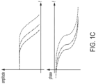
- FIG. 1C is a plot illustrating the amplitude response and the phase response associated with some of the paths of the TI ADC of FIG. 1A . These plots illustrate the amplitude response and phase response of three representative paths of the four paths of FIG. 1A . As can be appreciated from the top plot, each path exhibits a different frequency bandwidth. Further, as can be appreciated from the bottom plot, each path exhibits a different frequency at which the convexity of the corresponding phase is inverted.
- FIG. 2A is a plot that illustrates how the phase of the TI ADC of FIG. 1A varies over time.
- the overall phase associated with the signals appearing at the inputs the samplers presents a cyclical behavior.
- the TI ADC oscillates in accordance with the following values: ⁇ 1, ⁇ 2, ⁇ 3 and ⁇ 4.
- ⁇ 1 represents the phase associated with the first path of the TI ADC
- ⁇ 2 represents the phase associated with the second path
- ⁇ 3 represents the phase associated with the third path
- ⁇ 4 represents the phase associated with the fourth path.
- phase oscillation because, as different samplers are activated in a sequential fashion, the phase of the currently activated sampler is switched from one value to another.
- the phase cycles in accordance with the following sequence: ⁇ 1, ⁇ 2, ⁇ 3, ⁇ 4, ⁇ 1, ⁇ 2, ⁇ 3, ⁇ 4, ⁇ 1, ⁇ 2, ⁇ 3, ⁇ 4...
- the periodicity of the phase oscillation is four samples. Every four samples, the phase oscillation repeats itself. It is this phase oscillation that creates the spurious tones illustrated in FIG. 1D .
- a TI ADC has a set of N paths electrically coupled to the input terminal (e.g., four paths in the example of FIG. 1A ).
- the N paths result in a phase oscillation of the input signal as appearing at the samplers, where the phase oscillation presents at most N phase values (e.g., ⁇ 1, ⁇ 2, ⁇ 3, ⁇ 4).
- the phase oscillation oscillates in accordance with a first periodicity (a periodicity of four phase values in the example of FIG. 1A ).
- the techniques described herein involve controlling at least some of the N samplers to modify the phase oscillation of the input signal so that the modified phase oscillation presents more than N phase values.
- the modified phase oscillation oscillates in accordance with a second periodicity greater than the first periodicity (e.g., a periodicity greater than four phase values).
- FIG. 3A is a block diagram of a differential TI ADC arranged in this manner.
- Each path of the TI ADC includes a pair of switches SW1, a pair of switches SW2, switches SWe and a pair of sampling capacitors Cs.
- the timing with which the switches are activated and deactivated in some embodiments is illustrated in FIG. 3B .
- the signals depicted in FIG. 3B dictate the sample and hold operation of the TI ADC.
- FIG. 3C represents a single-ended implementation of a path of the TI ADC.
- the timing of the sampling is determined by the opening of the switches SWe.
- the main source of bandwidth mismatch is the on-resistance of the switches SW1, tied to a terminal of sampling capacitors Cs.
- increasing the periodicity of the phase oscillation from the first periodicity to the second periodicity can be accomplished by introducing additional capacitors in parallel to the capacitors Cs, and by varying the capacitances of these additional capacitors in accordance with random or pseudo random codes (thereby changing the time constant RC).
- FIG. 4A illustrates a diagram of a TI ADC path having one such parallel capacitor (Cr), the capacitance of which is set by a pseudo random noise generator (PN).
- FIG. 4B is a plot illustrating control signals for timing the operation of the circuit of FIG. 4A . In accordance with the plot of FIG. 4B , the total value of the sampling capacitor Cs of each of path can be adjusted.
- the total value of Cs is changed frequently, possibly each time a new sample is captured as depicted in FIG. 4B .
- a sampling capacitor Cs need not be updated whenever a new sample is captured.
- the corresponding bandwidth mismatch varies accordingly, and the original periodic sequence of fixed bandwidth mismatches is replaced by a random sequence of ever-changing bandwidth mismatches.
- correlation among the sampled input waveform is reduced, thus substantially improving the spurious free dynamic range (SFDR) of the TI ADC.
- the total sampling capacitance can be realized by shunting a main sampling capacitor (having capacitance of Cs- ⁇ C/2 (slightly smaller than the original Cs), with an additional small capacitor Cr the value of which is varied by the random digital code PN.
- ⁇ C determines the desired range of capacitance variation.
- the nominal value of Cr can be made adjustable from 0 to ⁇ C. As result, the total value of the sampling capacitance can be varied between Cs- ⁇ C/2 and CS+ ⁇ C/2.
- FIG. 4C is a diagram illustrating a circuit for varying the capacitance of a sampler, in accordance with some embodiments.
- a sampler includes P capacitors Cu, which are connected/disconnected from resistor R depending on the state of the corresponding transistors T A1 , T A2 , T A3 , T A4 and T AP , and are connected/disconnected from ground depending on the state of the corresponding transistors T B1 , T B2 , T B3 , T B4 and T BP .
- capacitance C M x C u .
- varying the sampling capacitors results in an increase of the periodicity of the phase oscillation.
- FIG. 5A An example of this result is depicted in FIG. 5A .
- the phase oscillation proceeds as in the example of FIG. 2B : the first phase value of the oscillation is ⁇ 1, the second phase value of the oscillation is ⁇ 2, and the third phase value of the oscillation is ⁇ 3.
- the phase oscillation of FIG. 5A proceeds to phase value ⁇ 4a, where ⁇ 4a is different from ⁇ 4. This can be accomplished by varying the capacitance of the fourth sampling capacitor from its nominal value.
- phase oscillation proceeds to phase value ⁇ 1a, where ⁇ 1a is different from ⁇ 1. This can be accomplished by varying the capacitance of the first sampling capacitor from its nominal value. Then, the phase oscillation proceeds to phase value ⁇ 2b, where ⁇ 2b is different from ⁇ 2. This can be accomplished by varying the capacitance of the second sampling capacitor from its nominal value. Then, the phase oscillation proceeds to phase value ⁇ 3b, where ⁇ 3b is different from ⁇ 3. This can be accomplished by varying the capacitance of the third sampling capacitor from its nominal value. Lastly, the phase oscillation proceeds to phase value ⁇ 4. This can be accomplished by setting the capacitance of the fourth sampling capacitor back to its nominal value. The phase oscillation then repeats itself.
- phase oscillation 5B provides a comparison between two TI ADCs each having four paths.
- the phase oscillation is unmodified and presents a periodicity of four phase values.
- the phase oscillation is modified in accordance with the scheme of FIG. 5A , and as a result presents a periodicity of eight phase values.
- FIG. 5C is a plot illustrating how the unmodified phase oscillation varies over time
- FIG. 5D is a plot illustrating the corresponding spectrum.
- the phase oscillation gives rise to a spurious tone having an amplitude (-52 dB) several orders of magnitude above the noise floor.
- FIG. 5E is a plot illustrating the phase of the oscillation when modified in accordance with the sequence of FIG. 5B
- FIG. 5F is a plot illustrating the corresponding spectrum.
- the modified phase oscillation deviates from a sinusoidal oscillation to a greater extent than the unmodified oscillation does. The result is that the energy of the spurious tone shown in FIG.
- Each tone of FIG. 5F has an amplitude that is significantly lower than the amplitude of the tone of FIG. 5D , thus reducing the negative effects of bandwidth mismatch on the performance of the TI ADC.
- the tone with the largest amplitude is 7dB less than the tone of FIG. 5D .
- the sequence of phase values appearing at the samplers may be varied in accordance with permutations of prime numbers. For instance, the sequence may be altered every five samples (five is a prime number).
- the inventor has appreciated that by varying the phase sequence in accordance with permutations of prime numbers leads to larger periodicities. The result is that the energy of a spurious tone is spread to an even greater extent.
- FIG. 6A illustrates the periodicity of a phase oscillation before and after modification using a permutation of a prime number, in accordance with some embodiments. In this example, the periodicity is increased from four phase values (in the unmodified case) to twenty phase values (in the modified case).
- FIG. 6B is a plot illustrating how the unmodified phase oscillation varies over time
- FIG. 6C is a plot illustrating the corresponding spectrum.
- the phase oscillation gives rise to a spurious tone having an amplitude of -50 dB.
- FIG. 6D is a plot illustrating the phase of the oscillation when modified in accordance with the sequence of FIG. 6A
- FIG. 6E is a plot illustrating the corresponding spectrum.
- the energy of the spurious tone shown in FIG. 6C is spread among several additional tones.
- Each tone of FIG. 6E has an amplitude that is significantly lower than the amplitude of the tone of FIG. 6C , thus reducing the negative effects of bandwidth mismatch on the performance of the TI ADC.
- the tone with the largest amplitude is 5dB less than the tone of FIG. 6C .
- the sequence of phase values appearing at the samplers may be varied in accordance with a random or pseudo-random cadence. For instance, the sequence may be altered every five samples at one cycle, every three samples at the following cycle, every four samples at the following cycles, etc.
- the inventor has appreciated that by varying the phase sequence in accordance with a random or pseudo-random cadence leads to even larger periodicities than what is shown in the previous examples. The result is that the energy of a spurious tone is spread to an even greater extent.
- FIG. 7A illustrates the periodicity of a phase oscillation before and after modification using a random or pseudo-random cadence, in accordance with some embodiments. In this example, the periodicity is increased from four phase values (in the unmodified case) to twenty-six phase values (in the modified case).
- FIG. 7B is a plot illustrating how the unmodified phase oscillation varies over time
- FIG. 7C is a plot illustrating the corresponding spectrum.
- the phase oscillation gives rise to a spurious tone having an amplitude of -52 dB.
- FIG. 7D is a plot illustrating the phase of the oscillation when modified in accordance with the random cadence of FIG. 7A
- FIG. 7E is a plot illustrating the corresponding spectrum.
- the energy of the spurious tone shown in FIG. 7C is spread among so many new tones that the majority of the tones that arise as a result disappears under the noise floor.
- Example 3 This occurs because of the random (or pseudo-random) nature of the scrambling process used in Example 3. The result is that the noise floor is raised. Some tones may still lie above the noise floor, but their amplitude is substantially reduced. For example, the amplitude of the largest tone is -60 dB, which represents an 8 dB improvement over FIG. 7C .
- FIGs. 8A and 8B are plots illustrating the amplitude response of a TI ADC before and after modification using the third example, respectively. More specifically, the plots represent the ADC's SFDR as a function of frequency.
- the unmodified scenario presents tones with an SFDR of about 60dBFS.
- the majority of the energy is spread across so many new tones that the energy of these tones disappears under the noise floor. As a result, the noise floor raises.
- the largest tones have an SFDR of 70dBFS, representing a 10dB improvement over FIG. 8A .
- a TI ADC including a set of N paths electrically coupled to an input terminal (e.g., terminal 104).
- Each path includes a sampler (e.g., sampler 106) configured to sample an input signal (e.g., Vin) appearing at the input terminal.
- the N paths result in a phase oscillation of the input signal as appearing at the samplers, where the phase oscillation presents at most N phase values.
- the phase oscillation may present four phase values or less where the TI ADC includes four paths as illustrated in the example of FIG. 1A .
- the phase oscillation oscillates in accordance with a first periodicity (e.g., four phase values in the example of FIG. 2A ).
- Control circuitry is configured to control at least some of the N samplers to modify the phase oscillation of the input signal so that the modified phase oscillation presents more than N phase values.
- the unmodified phase oscillation may present four phase values and the modified phase oscillation may present eight phase values, twenty phase values or twenty-six phase values, among a few possible examples.
- the modified phase oscillation oscillates in accordance with a second periodicity greater than the first periodicity. This increase in the periodicity of the phase oscillation spreads the energy of spurious tones across the frequency spectrum.
- the input signal as appearing at a first sampler of the N samplers presents a first phase value (e.g., ⁇ 1 as shown at the bottom panel of FIG. 5B ), and, at a second oscillation cycle subsequent to the first oscillation cycle, the input signal as appearing at the first sampler of the N samplers presents a second phase value (e.g., ⁇ 1a as shown at the bottom panel of FIG. 5B ) different from the first phase value.
- a first phase value e.g., ⁇ 1 as shown at the bottom panel of FIG. 5B
- a second phase value e.g., ⁇ 1a as shown at the bottom panel of FIG. 5B
- the input signal as appearing at a second sampler of the N samplers presents a third phase value (e.g., ⁇ 2 as shown at the bottom panel of FIG. 5B ), and, at the second oscillation cycle, the input signal as appearing at the second sampler of the N samplers presents a fourth phase value (e.g., ⁇ 2b as shown at the bottom panel of FIG. 5B ) different from the third phase value.
- a third phase value e.g., ⁇ 2 as shown at the bottom panel of FIG. 5B
- a fourth phase value e.g., ⁇ 2b as shown at the bottom panel of FIG. 5B
- Coupled or “connected” is meant to refer to circuit elements, or signals, that are either directly linked to one another or through intermediate components.
- the terms “approximately”, “substantially,” and “about” may be used to mean within ⁇ 10% of a target value in some embodiments.
- the terms “approximately” and “about” may include the target value.
Landscapes
- Engineering & Computer Science (AREA)
- Theoretical Computer Science (AREA)
- Analogue/Digital Conversion (AREA)
Abstract
Description
- Time interleaved (TI) analog-to-digital converters (ADC) sample input signals using multiple ADC units in a time-multiplexed fashion. TI ADCs are used in a broad variety of applications, including in high-end instrumentations, Radar and Lidar, and wireless infrastructure (e.g., 5G cellular towers).
- Some embodiments relate to a time-interleaved (TI) analog-to-digital converter (ADC), comprising: an input terminal; a set of N paths electrically coupled to the input terminal, each path comprising a sampler configured to sample an input signal appearing at the input terminal, wherein N is a positive integer, wherein the N paths result in a phase oscillation of the input signal as appearing at the samplers, wherein the phase oscillation presents at most N phase values, and wherein the phase oscillation oscillates in accordance with a first periodicity; and control circuitry configured to control at least some of the N samplers to modify the phase oscillation of the input signal so that the modified phase oscillation presents more than N phase values, and the modified phase oscillation oscillates in accordance with a second periodicity greater than the first periodicity.
- In some embodiments, controlling the at least some of the N samplers to modify the phase oscillation of the input signal comprises controlling the at least some of the N samplers so that: at a first oscillation cycle, the input signal as appearing at a first sampler of the N samplers presents a first phase value, and at a second oscillation cycle subsequent to the first oscillation cycle, the input signal as appearing at the first sampler of the N samplers presents a second phase value different from the first phase value.
- In some embodiments, controlling at least some of the N samplers to modify the phase oscillation of the input signal further comprises controlling the at least some of the N samplers so that: at the first oscillation cycle, the input signal as appearing at a second sampler of the N samplers presents a third phase value, and at the second oscillation cycle, the input signal as appearing at the second sampler of the N samplers presents a fourth phase value different from the third phase value.
- In some embodiments, a first sampler of the N samplers comprises P switches, wherein P is a positive integer, and wherein controlling the at least some of the N samplers to modify the phase oscillation of the input signal further comprises: at the first oscillation cycle, controlling the first sampler to maintain a first subset of the P switches active.
- In some embodiments, controlling at least some of the N samplers to modify the phase oscillation of the input signal further comprises: at the second oscillation cycle, controlling the first sampler to maintain a second subset of the P switches active, the second subset being different from the first subset.
- In some embodiments, the second periodicity is at least twice the first periodicity.
- In some embodiments, controlling at least some of the N samplers to modify the phase oscillation of the input signal comprises performing a phase permutation of the phase oscillation.
- In some embodiments, performing the phase permutation of the phase oscillation comprises performing the phase permutation of the phase oscillation in accordance with a prime number.
- In some embodiments, performing the phase permutation of the phase oscillation comprises performing the phase permutation of the phase oscillation in accordance with a random or pseudo-random cadence.
- In some embodiments, the control circuitry is configured to clock the N samplers so that each sampler samples the input signal appearing at the input terminal within a different time interval.
- Some embodiments relate to a method for controlling a time-interleaved (TI) analog-to-digital converter (ADC), comprising: receiving an input signal at each path of a set of N paths electrically coupled to an input terminal, wherein N is a positive integer, each path comprising a sampler configured to sample the input signal, wherein the N paths result in a phase oscillation of the input signal as appearing at the samplers, wherein the phase oscillation presents at most N phase values, and wherein the phase oscillation oscillates in accordance with a first periodicity; sampling the input signal with each sampler of the N samplers; and controlling at least some of the N samplers to modify the phase oscillation of the input signal so that the modified phase oscillation presents more than N phase values, and the modified phase oscillation oscillates in accordance with a second periodicity greater than the first periodicity.
- In some embodiments, controlling the at least some of the N samplers to modify the phase oscillation of the input signal comprises controlling the N samplers so that: at a first oscillation cycle, the input signal as appearing at a first sampler of the N samplers presents a first phase value, and at a second oscillation cycle subsequent to the first oscillation cycle, the input signal as appearing at the first sampler of the N samplers presents a second phase value different from the first phase value.
- In some embodiments, controlling the at least some of the N samplers to modify the phase oscillation of the input signal further comprises controlling the N samplers so that: at the first oscillation cycle, the input signal as appearing at a second sampler of the N samplers presents a third phase value, and at the second oscillation cycle, the input signal as appearing at the second sampler of the N samplers presents a fourth phase value different from the third phase value.
- In some embodiments, a first sampler of the N samplers comprises P switches, wherein P is a positive integer, and wherein controlling the at least some of the N samplers to modify the phase oscillation of the input signal further comprises: at the first oscillation cycle, controlling the first sampler to maintain a first subset of the P switches active.
- In some embodiments, controlling the at least some of the N samplers to modify the phase oscillation of the input signal further comprises: at the second oscillation cycle, controlling the first sampler to maintain a second subset of the P switches active, the second subset being different from the first subset.
- In some embodiments, the second periodicity is at least twice the first periodicity.
- In some embodiments, controlling the at least some of the N samplers to modify the phase oscillation of the input signal comprises performing a phase permutation of the phase oscillation.
- In some embodiments, performing the phase permutation of the phase oscillation comprises performing the phase permutation of the phase oscillation in accordance with a prime number.
- In some embodiments, performing the phase permutation of the phase oscillation comprises performing the phase permutation of the phase oscillation in accordance with a random or pseudo-random cadence.
- In some embodiments, sampling the input signal with each sampler of the N samplers comprises clocking the N samplers so that each sampler samples the input signal within a different time interval.
- The foregoing summary is provided by way of illustration and is not intended to be limiting.
- The accompanying drawings are not intended to be drawn to scale. In the drawings, each identical or nearly identical component that is illustrated in various figures is represented by a like numeral. For purposes of clarity, not every component may be labeled in every drawing.
-
FIG. 1A is a block diagram of a time interleaved (TI) analog-to-digital converters (ADC) suffering from bandwidth mismatch, in accordance with some embodiments. -
FIG. 1B is a plot illustrating clock signals for timing the operation of the TI ADC ofFIG. 1A , in accordance with some embodiments. -
FIG. 1C is a plot illustrating the amplitude response and the phase response associated with some of the paths of the TI ADC ofFIG. 1A , in accordance with some embodiments. -
FIG. 1D is a plot illustrating the amplitude response associated with the TI ADC ofFIG. 1A , in accordance with some embodiments. -
FIG. 2A is a plot illustrating a phase oscillation associated with the TI ADC ofFIG. 1A , in accordance with some embodiments. -
FIG. 2B is a plot illustrating how the phase of the input signal jumps between different paths of the TI ADC ofFIG. 1A , in accordance with some embodiments. -
FIG. 3A is a block diagram of a differential TI ADC configured to mitigate bandwidth mismatch, in accordance with some embodiments. -
FIG. 3B is a plot illustrating control signals for timing the operation of the TI ADC ofFIG. 3A , in accordance with some embodiments. -
FIG. 3C is a block diagram of a single-ended TI ADC configured to mitigate bandwidth mismatch, in accordance with some embodiments. -
FIG. 4A is a block diagram illustrating a pseudo random noise generator in addition to the single-ended TI ADC ofFIG. 3C , in accordance with some embodiments. -
FIG. 4B is a plot illustrating control signals for timing the operation of the TI ADC ofFIG. 4A , in accordance with some embodiments. -
FIG. 4C is a diagram illustrating a circuit for varying the capacitance of a sampler, in accordance with some embodiments. -
FIG. 5A is a plot illustrating a technique for extending the periodicity of a phase oscillation, in accordance with some embodiments. -
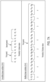
FIG. 5B illustrates the periodicity of a phase oscillation before and after modification using a first example, in accordance with some embodiments. -
FIG. 5C is a plot illustrating a phase oscillation before modification using the first example, in accordance with some embodiments. -
FIG. 5D is a plot illustrating an amplitude response associated with the phase oscillation ofFIG. 5C , in accordance with some embodiments. -
FIG. 5E is a plot illustrating a phase oscillation after modification using the first example, in accordance with some embodiments. -
FIG. 5F is a plot illustrating an amplitude response associated with phase oscillation after modification using the first example, in accordance with some embodiments. -
FIG. 6A illustrates the periodicity of a phase oscillation before and after modification using a second example, in accordance with some embodiments. -
FIG. 6B is a plot illustrating a phase oscillation before modification using the second example, in accordance with some embodiments. -
FIG. 6C is a plot illustrating an amplitude response associated with the phase oscillation ofFIG. 6B , in accordance with some embodiments. -
FIG. 6D is a plot illustrating a phase oscillation after modification using the second example, in accordance with some embodiments. -
FIG. 6E is a plot illustrating an amplitude response associated with phase oscillation after modification using the second example, in accordance with some embodiments. -
FIG. 7A illustrates the periodicity of a phase oscillation before and after modification using a third example, in accordance with some embodiments. -
FIG. 7B is a plot illustrating a phase oscillation before modification using the third example, in accordance with some embodiments. -
FIG. 7C is a plot illustrating an amplitude response associated with the phase oscillation ofFIG. 7B , in accordance with some embodiments. -
FIG. 7D is a plot illustrating a phase oscillation after modification using the third example, in accordance with some embodiments. -
FIG. 7E is a plot illustrating an amplitude response associated with phase oscillation after modification using the third example, in accordance with some embodiments. -
FIG. 8A is a plot illustrating the amplitude response of a TI ADC before modification using the third example, in accordance with some embodiments. -
FIG. 8B is a plot illustrating the amplitude response of a TI ADC after modification using the third example, in accordance with some embodiments. - The inventor has recognized and appreciated that time interleaved (TI) analog-to-digital converters (ADC) suffer from four types of mismatch-offset mismatch, gain mismatch, time skew mismatch and bandwidth mismatch. Collectively, these phenomena degrade the integrity of the output signal, and as a result, the performance of the TI ADC. The inventor has developed techniques for mitigating bandwidth mismatch, the type of mismatch that affects the integrity of the output signal the most in most circumstances.
- Bandwidth mismatch occurs because the paths that connect the input terminal of a TI ADC to the various samplers present different time constants (e.g., RC). In some circumstances, the major contributor is the fact that the sampling switches present different values of resistance and/or capacitance. Bandwidth mismatch results in a phase oscillation across the input terminals of the samplers. The phase oscillation, in turn, gives rise to spurious tones in the spectral response of the converter that are substantially above the noise floor. The presence of these tones may be unacceptable in some contexts (e.g., in high-end instrumentations, Radar and Lidar, and wireless infrastructure).
- The techniques developed by the inventor and described herein involve spreading the energy associated with the spurious tones across the frequency spectrum, thereby reducing the overall impact of individual tones. In some embodiments, for example, the tones may disappear under the noise floor. Spreading the energy associated with the spurious tones can be achieved by increasing the periodicity of the phase oscillation. This, in turn, can be achieved by introducing, in the phase oscillation, artificial phase shifts in addition to the phase shifts arising due to bandwidth mismatch. In one example, increasing the periodicity of a phase oscillation from 4 phase samples to 8 phase samples can result in a reduction in the power of a tone as high as 7 dB.
- Bandwidth mismatch is a result of the fact that the paths that connect the input terminal of a TI ADC to the various samplers inevitably present different time constants.
FIG. 1 is a block diagram illustrating a TI ADC that suffers from bandwidth mismatch.TI ADC 100 includes aninput buffer 102, aninput terminal 104, and a plurality of paths (four paths in this example, though more or fewer paths are also possible). Each path includes asampler 106 andmultiple ADCs 108 connected to the sampler. For example,path 105 includes asampler 106 andADCs input terminal 104 is voltage Vin. Control circuitry 110 generates the clock signals (ck1, ck2, ck3 and ck4) used to time the operation ofTI ADC 100. Examples of the clock signals are illustrated inFIG. 1B . Here, a clock having a high value indicates that thecorresponding sampler 106 is supposed to sample the input signal. By contrast, a clock having a low value indicates that thecorresponding sampler 106 is not supposed to sample the input signal. Other logics are also possible. As can be appreciated fromFIG. 1B ,control circuitry 110 controls the TI ADC so that each sampler samples the input signal at a different time interval, thus providing the desired time interleaving effect that enables higher sampling rates. - Referring back to
FIG. 1A , each path presents a certain resistance and capacitance, which results from the combination of the resistance and capacitance of the conductive traces and the input resistance of the samplers. In theory, the TI ADC is designed so that the resistances and capacitances of the various paths are perfectly matched. In practice, however, the resistances and/or capacitance are slightly mismatched due to inevitable variations in the manufacturing processes. Variations in the input resistance and/or capacitance of the samplers can be particularly serious. In some circumstances, even the slightest variation in input resistance or capacitance (e.g., in the order of 0.5%) can produce unacceptable results. - The variations in resistance and capacitance described above are what causes bandwidth mismatch. As a result, each path exhibits a different frequency response to input signals.
FIG. 1C is a plot illustrating the amplitude response and the phase response associated with some of the paths of the TI ADC ofFIG. 1A . These plots illustrate the amplitude response and phase response of three representative paths of the four paths ofFIG. 1A . As can be appreciated from the top plot, each path exhibits a different frequency bandwidth. Further, as can be appreciated from the bottom plot, each path exhibits a different frequency at which the convexity of the corresponding phase is inverted. Collectively, these effects result in the formation of spurious tones, although the impact of the phase response tends to be larger than the impact of the amplitude response because, at least in some embodiments, the sampling rate of one sampler (e.g., 10 GHz) is lower than the cut-off frequency of the path (e.g.,25 GHz). Examples of these tones are depicted inFIG 1D . In this example, although the input signal exhibits a single frequency tone (the input frequency), the signal spectrum further exhibits spurious tones, which arise due to the differences in the frequency responses shown inFIG. 1C . These tones can seriously degrade the performance of the TI ADC. - The mismatch in the amplitude and phase responses associated with the different paths gives rise to a phase oscillation.
FIG. 2A is a plot that illustrates how the phase of the TI ADC ofFIG. 1A varies over time. As can be appreciated from this figure, the overall phase associated with the signals appearing at the inputs the samplers presents a cyclical behavior. Here, the TI ADC oscillates in accordance with the following values: Φ1, Φ2, Φ3 and Φ4. Φ1 represents the phase associated with the first path of the TI ADC, Φ2 represents the phase associated with the second path, Φ3 represents the phase associated with the third path, and Φ4 represents the phase associated with the fourth path. The phase shown inFIG. 2A oscillates because, as different samplers are activated in a sequential fashion, the phase of the currently activated sampler is switched from one value to another. In essence, as further shown inFIG. 2B , the phase cycles in accordance with the following sequence: Φ1, Φ2, Φ3, Φ4, Φ1, Φ2, Φ3, Φ4, Φ1, Φ2, Φ3, Φ4...Here, the periodicity of the phase oscillation is four samples. Every four samples, the phase oscillation repeats itself. It is this phase oscillation that creates the spurious tones illustrated inFIG. 1D . - Described herein are techniques for mitigating bandwidth mismatch in TI ADCs. In some embodiments, this may be accomplished by spreading the energy associated with the spurious tones across the frequency spectrum. In this way, the overall impact of each individual tone is reduced substantially. In some embodiments, for example, the tones may disappear under the noise floor. Spreading the energy associated with the spurious tones can be achieved by increasing the periodicity of the phase oscillation discussed above. This, in turn, can be achieved by introducing artificial phase shifts in addition to the phase shifts arising due to bandwidth mismatch.
- In one example, a TI ADC has a set of N paths electrically coupled to the input terminal (e.g., four paths in the example of
FIG. 1A ). The N paths result in a phase oscillation of the input signal as appearing at the samplers, where the phase oscillation presents at most N phase values (e.g., Φ1, Φ2, Φ3, Φ4). The phase oscillation oscillates in accordance with a first periodicity (a periodicity of four phase values in the example ofFIG. 1A ). The techniques described herein involve controlling at least some of the N samplers to modify the phase oscillation of the input signal so that the modified phase oscillation presents more than N phase values. As a result, the modified phase oscillation oscillates in accordance with a second periodicity greater than the first periodicity (e.g., a periodicity greater than four phase values). -
FIG. 3A is a block diagram of a differential TI ADC arranged in this manner. Each path of the TI ADC includes a pair of switches SW1, a pair of switches SW2, switches SWe and a pair of sampling capacitors Cs. The timing with which the switches are activated and deactivated in some embodiments is illustrated inFIG. 3B . The signals depicted inFIG. 3B dictate the sample and hold operation of the TI ADC.FIG. 3C represents a single-ended implementation of a path of the TI ADC. The timing of the sampling is determined by the opening of the switches SWe. The main source of bandwidth mismatch is the on-resistance of the switches SW1, tied to a terminal of sampling capacitors Cs. - In some embodiments, increasing the periodicity of the phase oscillation from the first periodicity to the second periodicity can be accomplished by introducing additional capacitors in parallel to the capacitors Cs, and by varying the capacitances of these additional capacitors in accordance with random or pseudo random codes (thereby changing the time constant RC).
FIG. 4A illustrates a diagram of a TI ADC path having one such parallel capacitor (Cr), the capacitance of which is set by a pseudo random noise generator (PN).FIG. 4B is a plot illustrating control signals for timing the operation of the circuit ofFIG. 4A . In accordance with the plot ofFIG. 4B , the total value of the sampling capacitor Cs of each of path can be adjusted. The total value of Cs is changed frequently, possibly each time a new sample is captured as depicted inFIG. 4B . However, in some embodiments, a sampling capacitor Cs need not be updated whenever a new sample is captured. Thus, when Cs is varied, the corresponding bandwidth mismatch varies accordingly, and the original periodic sequence of fixed bandwidth mismatches is replaced by a random sequence of ever-changing bandwidth mismatches. As a result, correlation among the sampled input waveform is reduced, thus substantially improving the spurious free dynamic range (SFDR) of the TI ADC. - In some embodiments, the total sampling capacitance can be realized by shunting a main sampling capacitor (having capacitance of Cs-δC/2 (slightly smaller than the original Cs), with an additional small capacitor Cr the value of which is varied by the random digital code PN. Here, δC determines the desired range of capacitance variation. The nominal value of Cr can be made adjustable from 0 to δC. As result, the total value of the sampling capacitance can be varied between Cs-δC/2 and CS+δC/2.
- In some embodiments, varying the capacitance of a sampler may involve providing a sampler with multiple capacitors, and activating only sub-sets of these capacitors in a randomized (or pseudo-randomized) fashion.
FIG. 4C is a diagram illustrating a circuit for varying the capacitance of a sampler, in accordance with some embodiments. In this example, a sampler includes P capacitors Cu, which are connected/disconnected from resistor R depending on the state of the corresponding transistors TA1, TA2, TA3, TA4 and TAP, and are connected/disconnected from ground depending on the state of the corresponding transistors TB1, TB2, TB3, TB4 and TBP. In some embodiments, only a sub-set of M (<P) capacitors are activated, thereby providing an overall capacitance C = M x Cu. By varying which M capacitors are activated in a randomized (or pseudo-randomized) fashion, capacitance C can be randomized. - In some embodiments, varying the sampling capacitors results in an increase of the periodicity of the phase oscillation. An example of this result is depicted in
FIG. 5A . Initially, the phase oscillation proceeds as in the example ofFIG. 2B : the first phase value of the oscillation is Φ1, the second phase value of the oscillation is Φ2, and the third phase value of the oscillation is Φ3. Subsequently, instead of proceeding to Φ4 as shown inFIG. 2B , the phase oscillation ofFIG. 5A proceeds to phase value Φ4a, where Φ4a is different from Φ4. This can be accomplished by varying the capacitance of the fourth sampling capacitor from its nominal value. Then, the phase oscillation proceeds to phase value Φ1a, where Φ1a is different from Φ1. This can be accomplished by varying the capacitance of the first sampling capacitor from its nominal value. Then, the phase oscillation proceeds to phase value Φ2b, where Φ2b is different from Φ2. This can be accomplished by varying the capacitance of the second sampling capacitor from its nominal value. Then, the phase oscillation proceeds to phase value Φ3b, where Φ3b is different from Φ3. This can be accomplished by varying the capacitance of the third sampling capacitor from its nominal value. Lastly, the phase oscillation proceeds to phase value Φ4. This can be accomplished by setting the capacitance of the fourth sampling capacitor back to its nominal value. The phase oscillation then repeats itself.FIG. 5B provides a comparison between two TI ADCs each having four paths. In the top panel, the phase oscillation is unmodified and presents a periodicity of four phase values. In the bottom panel, the phase oscillation is modified in accordance with the scheme ofFIG. 5A , and as a result presents a periodicity of eight phase values. -
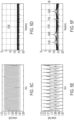
FIG. 5C is a plot illustrating how the unmodified phase oscillation varies over time, andFIG. 5D is a plot illustrating the corresponding spectrum. In this example, the phase oscillation gives rise to a spurious tone having an amplitude (-52 dB) several orders of magnitude above the noise floor. By contrast,FIG. 5E is a plot illustrating the phase of the oscillation when modified in accordance with the sequence ofFIG. 5B .FIG. 5F is a plot illustrating the corresponding spectrum. As can be appreciated by comparingFIG. 5C withFIG. 5E , the modified phase oscillation deviates from a sinusoidal oscillation to a greater extent than the unmodified oscillation does. The result is that the energy of the spurious tone shown inFIG. 5D is spread among several additional tones not otherwise present in the unmodified case. Each tone ofFIG. 5F has an amplitude that is significantly lower than the amplitude of the tone ofFIG. 5D , thus reducing the negative effects of bandwidth mismatch on the performance of the TI ADC. The tone with the largest amplitude is 7dB less than the tone ofFIG. 5D . - In another example, the sequence of phase values appearing at the samplers may be varied in accordance with permutations of prime numbers. For instance, the sequence may be altered every five samples (five is a prime number). The inventor has appreciated that by varying the phase sequence in accordance with permutations of prime numbers leads to larger periodicities. The result is that the energy of a spurious tone is spread to an even greater extent.
FIG. 6A illustrates the periodicity of a phase oscillation before and after modification using a permutation of a prime number, in accordance with some embodiments. In this example, the periodicity is increased from four phase values (in the unmodified case) to twenty phase values (in the modified case). -
FIG. 6B is a plot illustrating how the unmodified phase oscillation varies over time, andFIG. 6C is a plot illustrating the corresponding spectrum. In this example, the phase oscillation gives rise to a spurious tone having an amplitude of -50 dB. By contrast,FIG. 6D is a plot illustrating the phase of the oscillation when modified in accordance with the sequence ofFIG. 6A .FIG. 6E is a plot illustrating the corresponding spectrum. As can be appreciated by comparingFIG. 6C withFIG. 6E , the energy of the spurious tone shown inFIG. 6C is spread among several additional tones. Each tone ofFIG. 6E has an amplitude that is significantly lower than the amplitude of the tone ofFIG. 6C , thus reducing the negative effects of bandwidth mismatch on the performance of the TI ADC. The tone with the largest amplitude is 5dB less than the tone ofFIG. 6C . - In yet another example, the sequence of phase values appearing at the samplers may be varied in accordance with a random or pseudo-random cadence. For instance, the sequence may be altered every five samples at one cycle, every three samples at the following cycle, every four samples at the following cycles, etc. The inventor has appreciated that by varying the phase sequence in accordance with a random or pseudo-random cadence leads to even larger periodicities than what is shown in the previous examples. The result is that the energy of a spurious tone is spread to an even greater extent.
FIG. 7A illustrates the periodicity of a phase oscillation before and after modification using a random or pseudo-random cadence, in accordance with some embodiments. In this example, the periodicity is increased from four phase values (in the unmodified case) to twenty-six phase values (in the modified case). -
FIG. 7B is a plot illustrating how the unmodified phase oscillation varies over time, andFIG. 7C is a plot illustrating the corresponding spectrum. In this example, the phase oscillation gives rise to a spurious tone having an amplitude of -52 dB. By contrast,FIG. 7D is a plot illustrating the phase of the oscillation when modified in accordance with the random cadence ofFIG. 7A .FIG. 7E is a plot illustrating the corresponding spectrum. As can be appreciated by comparingFIG. 7C withFIG. 7E , the energy of the spurious tone shown inFIG. 7C is spread among so many new tones that the majority of the tones that arise as a result disappears under the noise floor. This occurs because of the random (or pseudo-random) nature of the scrambling process used in Example 3. The result is that the noise floor is raised. Some tones may still lie above the noise floor, but their amplitude is substantially reduced. For example, the amplitude of the largest tone is -60 dB, which represents an 8 dB improvement overFIG. 7C . -
FIGs. 8A and 8B are plots illustrating the amplitude response of a TI ADC before and after modification using the third example, respectively. More specifically, the plots represent the ADC's SFDR as a function of frequency. The unmodified scenario presents tones with an SFDR of about 60dBFS. Upon application of the technique described in accordance with the third example, the majority of the energy is spread across so many new tones that the energy of these tones disappears under the noise floor. As a result, the noise floor raises. Here, the largest tones have an SFDR of 70dBFS, representing a 10dB improvement overFIG. 8A . - Accordingly, some embodiments relate to a TI ADC including a set of N paths electrically coupled to an input terminal (e.g., terminal 104). Each path includes a sampler (e.g., sampler 106) configured to sample an input signal (e.g., Vin) appearing at the input terminal. Due to bandwidth mismatch, the N paths result in a phase oscillation of the input signal as appearing at the samplers, where the phase oscillation presents at most N phase values. For example, the phase oscillation may present four phase values or less where the TI ADC includes four paths as illustrated in the example of
FIG. 1A . The phase oscillation oscillates in accordance with a first periodicity (e.g., four phase values in the example ofFIG. 2A ). Control circuitry is configured to control at least some of the N samplers to modify the phase oscillation of the input signal so that the modified phase oscillation presents more than N phase values. For example, the unmodified phase oscillation may present four phase values and the modified phase oscillation may present eight phase values, twenty phase values or twenty-six phase values, among a few possible examples. Accordingly, the modified phase oscillation oscillates in accordance with a second periodicity greater than the first periodicity. This increase in the periodicity of the phase oscillation spreads the energy of spurious tones across the frequency spectrum. - In some embodiments, at a first oscillation cycle, the input signal as appearing at a first sampler of the N samplers presents a first phase value (e.g., Φ1 as shown at the bottom panel of
FIG. 5B ), and, at a second oscillation cycle subsequent to the first oscillation cycle, the input signal as appearing at the first sampler of the N samplers presents a second phase value (e.g., Φ1a as shown at the bottom panel ofFIG. 5B ) different from the first phase value. - Further, in some embodiments, at the first oscillation cycle, the input signal as appearing at a second sampler of the N samplers presents a third phase value (e.g., Φ2 as shown at the bottom panel of
FIG. 5B ), and, at the second oscillation cycle, the input signal as appearing at the second sampler of the N samplers presents a fourth phase value (e.g., Φ2b as shown at the bottom panel ofFIG. 5B ) different from the third phase value. - Use of ordinal terms such as "first", "second", "third", etc., in the claims to modify a claim element does not by itself connote any priority, precedence, or order of one claim element over another or the temporal order in which acts of a method are performed, but are used merely as labels to distinguish one claim element having a certain name from another element having a same name (but for use of the ordinal term) to distinguish the claim elements.
- Also, the phraseology and terminology used herein is for the purpose of description and should not be regarded as limiting. The use of "including", "comprising", "having", "containing" or "involving" and variations thereof herein, is meant to encompass the items listed thereafter and equivalents thereof as well as additional items.
- The use of "coupled" or "connected" is meant to refer to circuit elements, or signals, that are either directly linked to one another or through intermediate components.
- The terms "approximately", "substantially," and "about" may be used to mean within ±10% of a target value in some embodiments. The terms "approximately" and "about" may include the target value.
Claims (15)
- A time-interleaved (TI) analog-to-digital converter (ADC), comprising:an input terminal;a set of N paths electrically coupled to the input terminal, each path comprising a sampler configured to sample an input signal appearing at the input terminal, wherein N is a positive integer, wherein the N paths result in a phase oscillation of the input signal as appearing at the samplers, wherein the phase oscillation presents at most N phase values, and wherein the phase oscillation oscillates in accordance with a first periodicity; andcontrol circuitry configured to control at least some of the N samplers to modify the phase oscillation of the input signal so that the modified phase oscillation presents more than N phase values, and the modified phase oscillation oscillates in accordance with a second periodicity greater than the first periodicity.
- The TI ADC of claim 1, wherein controlling the at least some of the N samplers to modify the phase oscillation of the input signal comprises controlling the at least some of the N samplers so that:at a first oscillation cycle, the input signal as appearing at a first sampler of the N samplers presents a first phase value, andat a second oscillation cycle subsequent to the first oscillation cycle, the input signal as appearing at the first sampler of the N samplers presents a second phase value different from the first phase value.
- The TI ADC of claim 2, wherein controlling at least some of the N samplers to modify the phase oscillation of the input signal further comprises controlling the at least some of the N samplers so that:at the first oscillation cycle, the input signal as appearing at a second sampler of the N samplers presents a third phase value, andat the second oscillation cycle, the input signal as appearing at the second sampler of the N samplers presents a fourth phase value different from the third phase value.
- The TI ADC of claim 2 or 3, wherein a first sampler of the N samplers comprises P switches, wherein P is a positive integer, and wherein controlling the at least some of the N samplers to modify the phase oscillation of the input signal further comprises:
at the first oscillation cycle, controlling the first sampler to maintain a first subset of the P switches active. - The TI ADC of claim 4, wherein controlling at least some of the N samplers to modify the phase oscillation of the input signal further comprises:
at the second oscillation cycle, controlling the first sampler to maintain a second subset of the P switches active, the second subset being different from the first subset. - The TI ADC of any one of the preceding claims, wherein controlling at least some of the N samplers to modify the phase oscillation of the input signal comprises performing a phase permutation of the phase oscillation.
- The TI ADC of claim 6, wherein performing the phase permutation of the phase oscillation comprises performing the phase permutation of the phase oscillation in accordance with a prime number and/or with a random or pseudo-random cadence.
- The TI ADC of any one of the preceding claims, wherein the control circuitry is configured to clock the N samplers so that each sampler samples the input signal appearing at the input terminal within a different time interval.
- A method for controlling a time-interleaved (TI) analog-to-digital converter (ADC), comprising:receiving an input signal at each path of a set of N paths electrically coupled to an input terminal, wherein N is a positive integer, each path comprising a sampler configured to sample the input signal, wherein the N paths result in a phase oscillation of the input signal as appearing at the samplers, wherein the phase oscillation presents at most N phase values, and wherein the phase oscillation oscillates in accordance with a first periodicity;sampling the input signal with each sampler of the N samplers; andcontrolling at least some of the N samplers to modify the phase oscillation of the input signal so that the modified phase oscillation presents more than N phase values, and the modified phase oscillation oscillates in accordance with a second periodicity greater than the first periodicity.
- The method of claim 9, wherein controlling the at least some of the N samplers to modify the phase oscillation of the input signal comprises controlling the N samplers so that:at a first oscillation cycle, the input signal as appearing at a first sampler of the N samplers presents a first phase value, andat a second oscillation cycle subsequent to the first oscillation cycle, the input signal as appearing at the first sampler of the N samplers presents a second phase value different from the first phase value.
- The method of claim 10, wherein controlling the at least some of the N samplers to modify the phase oscillation of the input signal further comprises controlling the N samplers so that:at the first oscillation cycle, the input signal as appearing at a second sampler of the N samplers presents a third phase value, andat the second oscillation cycle, the input signal as appearing at the second sampler of the N samplers presents a fourth phase value different from the third phase value.
- The method of claim 10 or 11, wherein a first sampler of the N samplers comprises P switches, wherein P is a positive integer, and wherein controlling the at least some of the N samplers to modify the phase oscillation of the input signal further comprises:
at the first oscillation cycle, controlling the first sampler to maintain a first subset of the P switches active. - The method of claim 12, wherein controlling the at least some of the N samplers to modify the phase oscillation of the input signal further comprises:
at the second oscillation cycle, controlling the first sampler to maintain a second subset of the P switches active, the second subset being different from the first subset. - The method of any one of claims 9 to 13, wherein controlling the at least some of the N samplers to modify the phase oscillation of the input signal comprises performing a phase permutation of the phase oscillation.
- The method of claim 14, wherein performing the phase permutation of the phase oscillation comprises performing the phase permutation of the phase oscillation in accordance with a prime number and/or with a random or pseudo-random cadence.
Applications Claiming Priority (2)
| Application Number | Priority Date | Filing Date | Title |
|---|---|---|---|
| US202263320748P | 2022-03-17 | 2022-03-17 | |
| US17/982,339 US12231140B2 (en) | 2022-03-17 | 2022-11-07 | Mitigation of undesired spectral images due to bandwidth mismatch in time-interleaved A/DS by sampling capacitance randomization |
Publications (2)
| Publication Number | Publication Date |
|---|---|
| EP4246813A1 true EP4246813A1 (en) | 2023-09-20 |
| EP4246813B1 EP4246813B1 (en) | 2025-12-31 |
Family
ID=85462229
Family Applications (1)
| Application Number | Title | Priority Date | Filing Date |
|---|---|---|---|
| EP23159788.1A Active EP4246813B1 (en) | 2022-03-17 | 2023-03-02 | Attenuation of undesirable spectral images due to bandwidth mismatch in time-nested ADCs by sampling capacity randomization |
Country Status (3)
| Country | Link |
|---|---|
| US (1) | US12231140B2 (en) |
| EP (1) | EP4246813B1 (en) |
| TW (1) | TWI863108B (en) |
Citations (2)
| Publication number | Priority date | Publication date | Assignee | Title |
|---|---|---|---|---|
| US7292170B2 (en) * | 2005-06-13 | 2007-11-06 | Texas Instruments Incorporated | System and method for improved time-interleaved analog-to-digital converter arrays |
| US20210359694A1 (en) * | 2020-05-15 | 2021-11-18 | Realtek Semiconductor Corporation | Time interleaved analog-to-digital converter |
Family Cites Families (19)
| Publication number | Priority date | Publication date | Assignee | Title |
|---|---|---|---|---|
| JP3839705B2 (en) * | 2001-11-21 | 2006-11-01 | アジレント・テクノロジーズ・インク | Sampling method and apparatus, and estimation method and apparatus |
| US7015842B1 (en) * | 2005-01-12 | 2006-03-21 | Teranetics, Inc. | High-speed sampling architectures |
| KR101376255B1 (en) * | 2009-03-03 | 2014-03-24 | 인터디지탈 패튼 홀딩스, 인크 | Method for a radio frequency (rf) sampling apparatus with arrays of time interleaved samplers and scenario based dynamic resource allocation |
| JP2012070087A (en) * | 2010-09-21 | 2012-04-05 | Toshiba Corp | Digital phase comparator and digital phase synchronization circuit |
| US8890739B2 (en) * | 2012-12-05 | 2014-11-18 | Crest Semiconductors, Inc. | Time interleaving analog-to-digital converter |
| US8810442B1 (en) * | 2013-02-14 | 2014-08-19 | Pmc-Sierra Us, Inc. | Background calibration of aperture center errors in analog to digital converters |
| TWI605688B (en) | 2013-03-08 | 2017-11-11 | 安娜卡敦設計公司 | Efficient time-interleaved analog-to-digital converter |
| US9214951B1 (en) * | 2014-05-30 | 2015-12-15 | Realtek Semiconductor Corp. | Self-calibrating VCO-based analog-to-digital converter and method thereof |
| US10341145B2 (en) * | 2015-03-03 | 2019-07-02 | Intel Corporation | Low power high speed receiver with reduced decision feedback equalizer samplers |
| US9680489B2 (en) * | 2015-10-02 | 2017-06-13 | Multiphy Ltd. | Background calibration of sampler offsets in analog to digital converters |
| US9692436B2 (en) * | 2015-10-22 | 2017-06-27 | Multiphy Ltd. | Background calibration of sampler timing errors in flash analog to digital converters |
| US9871504B2 (en) * | 2016-02-16 | 2018-01-16 | Analog Devices, Inc. | Differential phase adjustment of clock input signals |
| US9793910B1 (en) | 2016-09-12 | 2017-10-17 | Analog Devices, Inc. | Time-interleaved ADCs with programmable phases |
| US10608654B2 (en) * | 2017-10-27 | 2020-03-31 | Analog Devices, Inc. | Track and hold circuits for high speed and interleaved ADCS |
| TWI699975B (en) | 2019-08-30 | 2020-07-21 | 創意電子股份有限公司 | Analog to digital converter device and method for calibrating clock skew |
| US11349491B2 (en) * | 2020-03-04 | 2022-05-31 | Omni Design Technologies, Inc. | Time-interleaved sampling circuits with randomized skipping |
| US11082054B1 (en) * | 2020-06-26 | 2021-08-03 | Intel Corporation | Apparatus and method for time-interleaved analog-to-digital conversion |
| US11277146B2 (en) * | 2020-06-26 | 2022-03-15 | Intel Corporation | Analog-to-digital converter |
| US11621718B2 (en) * | 2020-10-28 | 2023-04-04 | Mediatek Singapore Pte. Ltd. | Analog-to-digital converter system using reference analog-to-digital converter with sampling point shifting and associated calibration method |
-
2022
- 2022-11-07 US US17/982,339 patent/US12231140B2/en active Active
-
2023
- 2023-02-01 TW TW112103387A patent/TWI863108B/en active
- 2023-03-02 EP EP23159788.1A patent/EP4246813B1/en active Active
Patent Citations (2)
| Publication number | Priority date | Publication date | Assignee | Title |
|---|---|---|---|---|
| US7292170B2 (en) * | 2005-06-13 | 2007-11-06 | Texas Instruments Incorporated | System and method for improved time-interleaved analog-to-digital converter arrays |
| US20210359694A1 (en) * | 2020-05-15 | 2021-11-18 | Realtek Semiconductor Corporation | Time interleaved analog-to-digital converter |
Non-Patent Citations (1)
| Title |
|---|
| PARK YUNSOO ET AL: "A Scalable Bandwidth Mismatch Calibration Technique for Time-Interleaved ADCs", IEEE TRANSACTIONS ON CIRCUITS AND SYSTEMS I: REGULAR PAPERS, IEEE, US, vol. 63, no. 11, 1 November 2016 (2016-11-01), pages 1889 - 1897, XP011626813, ISSN: 1549-8328, [retrieved on 20161025], DOI: 10.1109/TCSI.2016.2593927 * |
Also Published As
| Publication number | Publication date |
|---|---|
| TW202339440A (en) | 2023-10-01 |
| US20230299784A1 (en) | 2023-09-21 |
| US12231140B2 (en) | 2025-02-18 |
| TWI863108B (en) | 2024-11-21 |
| EP4246813B1 (en) | 2025-12-31 |
Similar Documents
| Publication | Publication Date | Title |
|---|---|---|
| CN112702061B (en) | Successive Approximation Analog-to-Digital Converter | |
| TWI727797B (en) | Time interleaved analog-to-digital converter | |
| US6037887A (en) | Programmable gain for delta sigma analog-to-digital converter | |
| US7319425B2 (en) | Comparator-based switched capacitor circuit for scaled semiconductor fabrication processes | |
| US11063794B2 (en) | Continuous-time sampler circuits | |
| CA2562254C (en) | A method and system for analog to digital conversion using digital pulse width modulation (pwm) | |
| EP2555432B1 (en) | Successive approximation register ADC circuits and methods | |
| US20100271248A1 (en) | Ramp wave output circuit, analog/digital conversion circuit, and camera | |
| US7466257B2 (en) | Delta-sigma AD converter | |
| US6515611B1 (en) | Multistage analog-to-digital converter with amplifier component swapping for improved linearity | |
| US8212699B1 (en) | System and method for extending the overload range of a sigma delta ADC system by providing over-range quantization levels | |
| EP4246813B1 (en) | Attenuation of undesirable spectral images due to bandwidth mismatch in time-nested ADCs by sampling capacity randomization | |
| US20080191923A1 (en) | Method and apparatus for analog-to-digital conversion using switched capacitors | |
| JP3628463B2 (en) | Delta-sigma A / D converter | |
| CN119836751A (en) | Aliasing suppression in analog-to-digital converters (ADCs) | |
| Krishna et al. | A 1V second order delta sigma ADC in 130nm CMOS | |
| CN116781080A (en) | Time-interleaved analog-to-digital converter and method performed therewith | |
| WO2024220901A1 (en) | Improved discrete-time linear equalizer for discrete-time analog front-end | |
| Kurchuk et al. | GHz-range continuous-time programmable digital FIR with power dissipation that automatically adapts to signal activity | |
| US12028101B2 (en) | Receive chain linearization via time-interleaved and polyphase mixing of interleaved paths | |
| Aryanfar et al. | A quad channel 11-bit 1 GS/s 40 mW Collaborative ADC based enabling digital beamforming for 5G wireless | |
| US11750205B1 (en) | Current digital-to-analog converter with distributed reconstruction filtering | |
| KR100345668B1 (en) | Digital to analog converter for minimizing error due to mismatch of capacitors | |
| KR102814960B1 (en) | Fir filter embedded sar adc and its operation method | |
| Bernardinis et al. | Dynamic stage matching for parallel pipeline A/D converters |
Legal Events
| Date | Code | Title | Description |
|---|---|---|---|
| PUAI | Public reference made under article 153(3) epc to a published international application that has entered the european phase |
Free format text: ORIGINAL CODE: 0009012 |
|
| STAA | Information on the status of an ep patent application or granted ep patent |
Free format text: STATUS: THE APPLICATION HAS BEEN PUBLISHED |
|
| AK | Designated contracting states |
Kind code of ref document: A1 Designated state(s): AL AT BE BG CH CY CZ DE DK EE ES FI FR GB GR HR HU IE IS IT LI LT LU LV MC ME MK MT NL NO PL PT RO RS SE SI SK SM TR |
|
| STAA | Information on the status of an ep patent application or granted ep patent |
Free format text: STATUS: REQUEST FOR EXAMINATION WAS MADE |
|
| 17P | Request for examination filed |
Effective date: 20240319 |
|
| RBV | Designated contracting states (corrected) |
Designated state(s): AL AT BE BG CH CY CZ DE DK EE ES FI FR GB GR HR HU IE IS IT LI LT LU LV MC ME MK MT NL NO PL PT RO RS SE SI SK SM TR |
|
| RIC1 | Information provided on ipc code assigned before grant |
Ipc: H03M 1/06 20060101AFI20250618BHEP Ipc: H03M 1/08 20060101ALI20250618BHEP Ipc: H03M 1/12 20060101ALI20250618BHEP |
|
| GRAP | Despatch of communication of intention to grant a patent |
Free format text: ORIGINAL CODE: EPIDOSNIGR1 |
|
| STAA | Information on the status of an ep patent application or granted ep patent |
Free format text: STATUS: GRANT OF PATENT IS INTENDED |
|
| INTG | Intention to grant announced |
Effective date: 20250728 |
|
| GRAS | Grant fee paid |
Free format text: ORIGINAL CODE: EPIDOSNIGR3 |
|
| GRAA | (expected) grant |
Free format text: ORIGINAL CODE: 0009210 |
|
| STAA | Information on the status of an ep patent application or granted ep patent |
Free format text: STATUS: THE PATENT HAS BEEN GRANTED |
|
| AK | Designated contracting states |
Kind code of ref document: B1 Designated state(s): AL AT BE BG CH CY CZ DE DK EE ES FI FR GB GR HR HU IE IS IT LI LT LU LV MC ME MK MT NL NO PL PT RO RS SE SI SK SM TR |
|
| REG | Reference to a national code |
Ref country code: CH Ref legal event code: F10 Free format text: ST27 STATUS EVENT CODE: U-0-0-F10-F00 (AS PROVIDED BY THE NATIONAL OFFICE) Effective date: 20251231 Ref country code: GB Ref legal event code: FG4D |
|
| REG | Reference to a national code |
Ref country code: DE Ref legal event code: R096 Ref document number: 602023010234 Country of ref document: DE |
|
| REG | Reference to a national code |
Ref country code: IE Ref legal event code: FG4D |
|
| REG | Reference to a national code |
Ref country code: LT Ref legal event code: MG9D |
|
| PG25 | Lapsed in a contracting state [announced via postgrant information from national office to epo] |
Ref country code: NO Free format text: LAPSE BECAUSE OF FAILURE TO SUBMIT A TRANSLATION OF THE DESCRIPTION OR TO PAY THE FEE WITHIN THE PRESCRIBED TIME-LIMIT Effective date: 20260331 |
|
| PGFP | Annual fee paid to national office [announced via postgrant information from national office to epo] |
Ref country code: DE Payment date: 20260319 Year of fee payment: 4 |
|
| PG25 | Lapsed in a contracting state [announced via postgrant information from national office to epo] |
Ref country code: FI Free format text: LAPSE BECAUSE OF FAILURE TO SUBMIT A TRANSLATION OF THE DESCRIPTION OR TO PAY THE FEE WITHIN THE PRESCRIBED TIME-LIMIT Effective date: 20251231 Ref country code: HR Free format text: LAPSE BECAUSE OF FAILURE TO SUBMIT A TRANSLATION OF THE DESCRIPTION OR TO PAY THE FEE WITHIN THE PRESCRIBED TIME-LIMIT Effective date: 20251231 |
|
| PGFP | Annual fee paid to national office [announced via postgrant information from national office to epo] |
Ref country code: AT Payment date: 20260301 Year of fee payment: 4 |
|
| PG25 | Lapsed in a contracting state [announced via postgrant information from national office to epo] |
Ref country code: RS Free format text: LAPSE BECAUSE OF FAILURE TO SUBMIT A TRANSLATION OF THE DESCRIPTION OR TO PAY THE FEE WITHIN THE PRESCRIBED TIME-LIMIT Effective date: 20260331 |
|
| PGFP | Annual fee paid to national office [announced via postgrant information from national office to epo] |
Ref country code: FR Payment date: 20260212 Year of fee payment: 4 |
|
| PG25 | Lapsed in a contracting state [announced via postgrant information from national office to epo] |
Ref country code: LV Free format text: LAPSE BECAUSE OF FAILURE TO SUBMIT A TRANSLATION OF THE DESCRIPTION OR TO PAY THE FEE WITHIN THE PRESCRIBED TIME-LIMIT Effective date: 20251231 |
|
| PG25 | Lapsed in a contracting state [announced via postgrant information from national office to epo] |
Ref country code: BG Free format text: LAPSE BECAUSE OF FAILURE TO SUBMIT A TRANSLATION OF THE DESCRIPTION OR TO PAY THE FEE WITHIN THE PRESCRIBED TIME-LIMIT Effective date: 20251231 |
|
| REG | Reference to a national code |
Ref country code: NL Ref legal event code: MP Effective date: 20251231 |
|
| REG | Reference to a national code |
Ref country code: AT Ref legal event code: MK05 Ref document number: 1874616 Country of ref document: AT Kind code of ref document: T Effective date: 20251231 |
|
| PG25 | Lapsed in a contracting state [announced via postgrant information from national office to epo] |
Ref country code: NL Free format text: LAPSE BECAUSE OF FAILURE TO SUBMIT A TRANSLATION OF THE DESCRIPTION OR TO PAY THE FEE WITHIN THE PRESCRIBED TIME-LIMIT Effective date: 20251231 |
|
| PG25 | Lapsed in a contracting state [announced via postgrant information from national office to epo] |
Ref country code: LT Free format text: LAPSE BECAUSE OF FAILURE TO SUBMIT A TRANSLATION OF THE DESCRIPTION OR TO PAY THE FEE WITHIN THE PRESCRIBED TIME-LIMIT Effective date: 20251231 |
|
| PG25 | Lapsed in a contracting state [announced via postgrant information from national office to epo] |
Ref country code: SM Free format text: LAPSE BECAUSE OF FAILURE TO SUBMIT A TRANSLATION OF THE DESCRIPTION OR TO PAY THE FEE WITHIN THE PRESCRIBED TIME-LIMIT Effective date: 20251231 |
|
| PG25 | Lapsed in a contracting state [announced via postgrant information from national office to epo] |
Ref country code: ES Free format text: LAPSE BECAUSE OF FAILURE TO SUBMIT A TRANSLATION OF THE DESCRIPTION OR TO PAY THE FEE WITHIN THE PRESCRIBED TIME-LIMIT Effective date: 20251231 |
|
| PG25 | Lapsed in a contracting state [announced via postgrant information from national office to epo] |
Ref country code: PL Free format text: LAPSE BECAUSE OF FAILURE TO SUBMIT A TRANSLATION OF THE DESCRIPTION OR TO PAY THE FEE WITHIN THE PRESCRIBED TIME-LIMIT Effective date: 20251231 |
|
| PG25 | Lapsed in a contracting state [announced via postgrant information from national office to epo] |
Ref country code: IT Free format text: LAPSE BECAUSE OF FAILURE TO SUBMIT A TRANSLATION OF THE DESCRIPTION OR TO PAY THE FEE WITHIN THE PRESCRIBED TIME-LIMIT Effective date: 20251231 |
|
| PG25 | Lapsed in a contracting state [announced via postgrant information from national office to epo] |
Ref country code: AT Free format text: LAPSE BECAUSE OF FAILURE TO SUBMIT A TRANSLATION OF THE DESCRIPTION OR TO PAY THE FEE WITHIN THE PRESCRIBED TIME-LIMIT Effective date: 20251231 |
|
| PG25 | Lapsed in a contracting state [announced via postgrant information from national office to epo] |
Ref country code: EE Free format text: LAPSE BECAUSE OF FAILURE TO SUBMIT A TRANSLATION OF THE DESCRIPTION OR TO PAY THE FEE WITHIN THE PRESCRIBED TIME-LIMIT Effective date: 20251231 |
|
| PG25 | Lapsed in a contracting state [announced via postgrant information from national office to epo] |
Ref country code: IS Free format text: LAPSE BECAUSE OF FAILURE TO SUBMIT A TRANSLATION OF THE DESCRIPTION OR TO PAY THE FEE WITHIN THE PRESCRIBED TIME-LIMIT Effective date: 20260430 Ref country code: PT Free format text: LAPSE BECAUSE OF FAILURE TO SUBMIT A TRANSLATION OF THE DESCRIPTION OR TO PAY THE FEE WITHIN THE PRESCRIBED TIME-LIMIT Effective date: 20260430 |
|
| PG25 | Lapsed in a contracting state [announced via postgrant information from national office to epo] |
Ref country code: CZ Free format text: LAPSE BECAUSE OF FAILURE TO SUBMIT A TRANSLATION OF THE DESCRIPTION OR TO PAY THE FEE WITHIN THE PRESCRIBED TIME-LIMIT Effective date: 20251231 |
|
| PG25 | Lapsed in a contracting state [announced via postgrant information from national office to epo] |
Ref country code: SK Free format text: LAPSE BECAUSE OF FAILURE TO SUBMIT A TRANSLATION OF THE DESCRIPTION OR TO PAY THE FEE WITHIN THE PRESCRIBED TIME-LIMIT Effective date: 20251231 |
|
| PG25 | Lapsed in a contracting state [announced via postgrant information from national office to epo] |
Ref country code: SE Free format text: LAPSE BECAUSE OF FAILURE TO SUBMIT A TRANSLATION OF THE DESCRIPTION OR TO PAY THE FEE WITHIN THE PRESCRIBED TIME-LIMIT Effective date: 20251231 |