EP4246606A2 - Electrode manufacturing apparatus, method for manufacturing electrode, apparatus for manufacturing electrochemical device, and method for manufacturing electrochemical device - Google Patents
Electrode manufacturing apparatus, method for manufacturing electrode, apparatus for manufacturing electrochemical device, and method for manufacturing electrochemical device Download PDFInfo
- Publication number
- EP4246606A2 EP4246606A2 EP23158381.6A EP23158381A EP4246606A2 EP 4246606 A2 EP4246606 A2 EP 4246606A2 EP 23158381 A EP23158381 A EP 23158381A EP 4246606 A2 EP4246606 A2 EP 4246606A2
- Authority
- EP
- European Patent Office
- Prior art keywords
- liquid composition
- defect
- insulating layer
- electrode
- discharge
- Prior art date
- Legal status (The legal status is an assumption and is not a legal conclusion. Google has not performed a legal analysis and makes no representation as to the accuracy of the status listed.)
- Granted
Links
Images




Classifications
-
- H—ELECTRICITY
- H01—ELECTRIC ELEMENTS
- H01M—PROCESSES OR MEANS, e.g. BATTERIES, FOR THE DIRECT CONVERSION OF CHEMICAL ENERGY INTO ELECTRICAL ENERGY
- H01M10/00—Secondary cells; Manufacture thereof
- H01M10/04—Construction or manufacture in general
- H01M10/0404—Machines for assembling batteries
-
- H—ELECTRICITY
- H01—ELECTRIC ELEMENTS
- H01M—PROCESSES OR MEANS, e.g. BATTERIES, FOR THE DIRECT CONVERSION OF CHEMICAL ENERGY INTO ELECTRICAL ENERGY
- H01M4/00—Electrodes
- H01M4/02—Electrodes composed of, or comprising, active material
- H01M4/04—Processes of manufacture in general
- H01M4/0402—Methods of deposition of the material
- H01M4/0404—Methods of deposition of the material by coating on electrode collectors
-
- H—ELECTRICITY
- H01—ELECTRIC ELEMENTS
- H01M—PROCESSES OR MEANS, e.g. BATTERIES, FOR THE DIRECT CONVERSION OF CHEMICAL ENERGY INTO ELECTRICAL ENERGY
- H01M4/00—Electrodes
- H01M4/02—Electrodes composed of, or comprising, active material
- H01M4/04—Processes of manufacture in general
- H01M4/0402—Methods of deposition of the material
- H01M4/0411—Methods of deposition of the material by extrusion
-
- H—ELECTRICITY
- H01—ELECTRIC ELEMENTS
- H01M—PROCESSES OR MEANS, e.g. BATTERIES, FOR THE DIRECT CONVERSION OF CHEMICAL ENERGY INTO ELECTRICAL ENERGY
- H01M4/00—Electrodes
- H01M4/02—Electrodes composed of, or comprising, active material
- H01M4/64—Carriers or collectors
- H01M4/66—Selection of materials
- H01M4/665—Composites
- H01M4/667—Composites in the form of layers, e.g. coatings
-
- H—ELECTRICITY
- H01—ELECTRIC ELEMENTS
- H01M—PROCESSES OR MEANS, e.g. BATTERIES, FOR THE DIRECT CONVERSION OF CHEMICAL ENERGY INTO ELECTRICAL ENERGY
- H01M50/00—Constructional details or processes of manufacture of the non-active parts of electrochemical cells other than fuel cells, e.g. hybrid cells
- H01M50/40—Separators; Membranes; Diaphragms; Spacing elements inside cells
- H01M50/403—Manufacturing processes of separators, membranes or diaphragms
Definitions
- the electrode manufacturing apparatus 1 includes the discharger 5 as a means for discharging the liquid composition 24.
- the discharger 5 includes multiple nozzle arrays each having multiple nozzles arranged in a width direction of the discharge target material (the Y direction).
- the discharger 5 of the liquid composition 24 is provided so that the liquid composition 24 may be discharged through the nozzles toward the discharge target material.
- the discharger 5 includes a discharge unit for the liquid composition 24.
- the discharge unit for the liquid composition 24 includes an aggregation of functional parts and mechanisms involved in the discharge of the liquid composition 24 from the discharger 5.
- the discharge unit for the liquid composition 24 includes at least one out of configurations of a supply mechanism, a maintenance mechanism, and a liquid discharging head movement mechanism, as combined with the discharger 5.
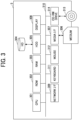
- FIG. 3 is a diagram illustrating a hardware configuration of the system control section 3.
- FIG. 2 as a function block diagram of the electrode manufacturing apparatus 1 includes a function block diagram of the system control section 3. Using FIGS. 2 and 3 , operations of the system control section 3 are described below.
- the system control section 3 includes the operation unit 34, the storage unit 35, the storage and reading unit 39, the processing unit 36, the surface detection image acquisition unit 51, the defect determination unit 52, the discharge instruction preparation unit 53, the result output unit 54, the conveyance control unit 33, and the discharge control unit 40.
- the operation unit 34 is chiefly realized by a command from the CPU 301 illustrated in FIG. 3 , and receives a signal from the keyboard 311 or the mouse 312 operated by the user, so as to accept various operations by the user.
- the operations thus accepted are each realized by a command from the CPU 301 illustrated in FIG. 3 , so as to cause various images or screens to be displayed on the display 308 provided on the operation unit 34.
- the processing unit 36 is realized by a command from the CPU 301 illustrated in FIG. 3 , and performs total control of the electrode manufacturing apparatus 1.
- the defect determination unit 52 distinguishes defects.
- the defect refers to a fault causing fall of a material characteristic value of the functional layer 12, such as a streak, a pinhole, unevenness, foreign matter, and a shortage of film thickness.
- An item in the quality information that should be regarded as a defect and such parameters as the size of a defect are assumed to be set by the user in advance. In a statement about FIGS. 6A through 6C to be given later, a streak-like defect is taken up.
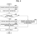
- FIG. 4 is a flowchart illustrating an example of processing for controlling the discharge amount.
- the surface detection image acquisition unit 51 acquires a surface detection image from the surface detector 8 (step S001).
- the defect determination unit 52 determines whether a streak-like defect is present (step S003), and, if the defect is not present, the log notifying that the change in discharge amount is unnecessary is prepared (step S004).
- the defect determination unit 52 instructs to prepare a discharge instruction (step S005), and the discharge instruction preparation unit 53 prepares an instruction to increase the discharge amount (step S006).
- a result with contents of the decided instruction is output from the result output unit 54 to the discharge control unit 40 (step S007).
- FIGS. 5A and 5B are conceptual diagrams of formation of the insulating layer 21 by the discharge of the liquid composition 24.
- FIGS. 5A and 5B a process for forming the insulating layer 21 in the electrode manufacturing apparatus 1 according to the present embodiment is described.
- FIG. 5A is a side view of the electrode manufacturing apparatus 1 as viewed in the Y direction
- FIG. 5B is a plan view of the electrode manufacturing apparatus 1 as viewed in a Z direction.
- FIGS. 5A and 5B the winding off part 10, the winding up part 11, the curing device 6, and the heater 7 illustrated in FIG. 1 is omitted for simplicity.
- the electrode manufacturing apparatus 1 uses the liquid composition 24 for forming the resin layer 22 or the inorganic layer 23 as the insulating layer 21 to form the resin layer 22 or the inorganic layer 23 as the insulating layer 21 so that the surface of the electrode base 9 or the surface of the functional layer 12 provided on the electrode base 9 may be covered, and detects the surface condition of the resin layer 22 or the inorganic layer 23 as the insulating layer 21 with the surface detector 8 provided downstream of the discharger 5.
- the electrode base 9 or the functional layer 12 provided on the electrode base 9 does not merely have a running pattern spread over the entire surface but may be formed by intermittent coating or in a free shape.
- a printing shape of the resin layer 22 or the inorganic layer 23 as the insulating layer 21, which is to be formed is not limited to a running pattern spread over the entire surface but may be achieved by intermittent coating or as a free shape.
- FIGS. 6A through 6C are plan views of the electrode manufacturing apparatus 1, illustrating how a streak-like defect is produced.
- FIGS. 6A through 6C description is made how a streak-like defect 59 is produced in the course of formation of the resin layer 22 or the inorganic layer 23 as the insulating layer 21.
- FIG. 6A illustrates a state where the streak-like defect 59 has been produced in the course of formation of the resin layer 22 or the inorganic layer 23 as the insulating layer 21. If the streak-like defect 59 has been produced in the course of discharge by the discharger 5, a log notifying that change in amount of discharge by the discharger 5 is unnecessary is only prepared (step S004) until the streak-like defect 59 reaches the surface detector 8.
- FIG. 6B illustrates a state where the streak-like defect 59 as produced in the course of formation of the resin layer 22 or the inorganic layer 23 as the insulating layer 21 has reached the surface detector 8. If the streak-like defect 59 reaches the surface detector 8, an instruction to increase the discharge amount is prepared by the discharge instruction preparation unit 53 (step S006). The instruction to increase the discharge amount is sent from the discharge instruction preparation unit 53 to the discharge control unit 40 through the result output unit 54 so as to increase the amount of discharge of the liquid composition 24 by the discharger 5.
- FIG. 6C illustrates a state after the instruction to increase the discharge amount is sent from the discharge instruction preparation unit 53 to the discharge control unit 40 through the result output unit 54 and the amount of discharge of the liquid composition 24 by the discharger 5 is increased.
- the discharge amount of the liquid composition 24 is increased so as to embed the streak-like defect 59 and suppress the production of another streak-like defect.
- FIGS. 7A through 7C are each another example of the diagram illustrating the general arrangement of the electrode manufacturing apparatus 1 according to the present embodiment.
- FIG. 7A illustrates the electrode manufacturing apparatus 1, which does not include the curing device 6 because the liquid composition 24 for forming the resin layer 22 or the inorganic layer 23 as the insulating layer 21 does not need a curing process.
- the surface detector 8 may be provided on an upstream side of the heater 7.
- the surface detector 8 is to detect the surface condition before drying of the liquid composition 24, the surface detector 8 is preferably provided at a stage next to the discharger 5 for the reason to be stated later.
- the surface detector 8 is preferably provided at the stage next to the discharger 5 for the reason to be stated later if the surface detector 8 is to detect the surface condition before the drying of the liquid composition 24.
- the present disclosure is chiefly effective at suppressing the production of the streak-like defect 59
- the insulating layer 21 after the production of the streak-like defect 59 illustrated in FIG. 6A is deemed to be faulty until the streak-like defect 59 is detected as illustrated in FIG. 6B and suppressed as illustrated in FIG. 6C . Therefore, the improvement in productivity attendant on the decrease in fraction defective is effected to a larger extent as the distance from the discharger 5 producing a defect to the surface detector 8 detecting a defect is shorter. Consequently, if a defect is detected before the drying of the liquid composition 24, it is desirable to provide the surface detector 8 immediately after the discharger 5, that is to say, at the stage next to the discharger 5.
- FIG. 8 illustrates an example of an optical system of the surface detector 8.
- the surface detector 8 includes, as an illumination system, a visible light source 62 that irradiates an upper face of a detection target 64 with a visible light, and an infrared/ultraviolet (IR/UV) light source 63 that emits at least one of an ultraviolet light or an infrared light.
- a visible light source 62 that irradiates an upper face of a detection target 64 with a visible light
- an infrared/ultraviolet (IR/UV) light source 63 that emits at least one of an ultraviolet light or an infrared light.
- the surface detector 8 may only include one of the light sources.
- the detection target 64 as an object of detection by the surface detector 8 refers to the electrode base 9 or the functional layer 12 provided on the electrode base 9, on which the resin layer 22 or the inorganic layer 23 as the insulating layer 21 is being formed.
- the surface detector 8 includes a visible light camera 61 as a measurement system, and the visible light camera 61 may be replaced by an IR/LTV light camera.
- the IR/UV light camera is to be arranged similarly to the visible light camera 61.
- the surface detector 8 detects a streak-like defect contained in the detection target 64, based on an output signal from the visible light camera 61 or the IR/UV light camera in such measurement system.
- FIG. 9A illustrates an example of a state where an image acquired by the surface detection image acquisition unit 51 after the detection of a defect by the surface detector 8 is displayed in the operation unit 34.
- defect type information 71 that is a result of analysis with the defect determination unit 52
- a defect spot line 73 and a defect output signal graph 74 (graph representing the change in output luminance value or luminance ratio) are collectively displayed.
- FIGS. 9B and 9C illustrate a case where the luminance value is high and a case where the luminance value is low, respectively.
- a correspondence relation between the pattern of such change (increase or decrease) in luminance value and the type of abnormality allows an accurate determination of the presence or absence of a defect and the level of a defect as a result of accumulation of experimental data for each type of abnormality that can actually occur.
- FIG. 10 is a flowchart of defect detection.
- a detection system is adjusted in a state where the detection target 64 is not arranged (step S301).
- a blue visible light source 31 is lit so as to perform image capturing with a visible light by an image capturing device 4.
- the luminance of light that directly enters the visible light camera 61 is so adjusted as to be the same or essentially the same as the upper limit of a measurable range.
- step S304 If it is determined that a defect has been detected (step S304), the processing proceeds to step S305. If it is determined that no defects have been detected (step S304), this routine is terminated.
- step S305 the type of the defect as detected is determined (step S305), and the type of the defect and defect spot information are output (step S306).
- FIG. 11 is a flowchart of discharge amount regulation based on defect spot information output.
- the surface detector 8, the surface detection image acquisition unit 51, and the defect determination unit 52 detect the defect spot information (step S401).
- the surface detection image acquisition unit 51 and the defect determination unit 52 specify the position (position in a y-axis direction) of the defect (step S402).
- the discharge instruction preparation unit 53 decides a discharge amount appropriate to the defect (an increased discharge amount, for instance) and a method for changing the discharge amount (change in discharge pattern or change in printing resolution, for instance) (step S403).
- the discharge control unit 40 controls the discharge with respect to the special position as instructed, based on the discharge amount and the discharge method as instructed (step S405).
- FIGS. 12A through 12D illustrate examples of the method for changing the discharge amount.
- the printing resolution in FIG. 12A is changed to the printing resolution in FIG. 12B .
- Such change in printing resolution is an exemplary method for increasing the discharge amount of the liquid composition 24.
- the printing resolution per unit area is changed from 3 ⁇ 3 in FIG. 12A to 4 ⁇ 4 in FIG. 12B .
- the printing resolution is changed from 3 ⁇ 3 to 4 ⁇ 4 without changing the size of dots to be printed, so as to increase the total discharge amount per unit area of the liquid composition 24.
- a printing pattern in FIG. 12C is changed to a printing pattern in FIG. 12D .
- Such change in printing pattern is another exemplary method for increasing the discharge amount of the liquid composition 24.
- the coverage rate is changed from about 56% in FIG. 12C to 100% in FIG. 12D so as to increase the total discharge amount per unit area of the liquid composition 24.
- the discharge amount may be increased over the entire region of discharge so as to embed the streak-like defect 59 or may be only increased on the periphery of a region of the streak-like defect 59.
- the surface detection image acquisition unit 51 and the defect determination unit 52 acquire information on the position in the Y direction of a defect, and the information on the position in the Y direction of a defect is additionally used by the discharge instruction preparation unit 53 to prepare a discharge instruction. In such case, the discharge amount does not need to be changed in a region other than the region of the streak-like defect 59, so that the film thickness is less affected as a whole.
- conveyance information (containing the conveyance speed and time information) on the electrode base 9 or the functional layer 12 provided on the electrode base 9, which is an object of conveyance, is considered to specify the position of a defect on the object of conveyance, as is the case with a normal production line.
- FIG. 13 is a flowchart of a method for gradually regulating the discharge amount.
- a defect is detected first and the position of the defect (the streak-like defect 59 in FIGS. 6A through 6C ) is specified.
- the position of the streak-like defect 59 on the electrode base 9 or the functional layer 12 provided on the electrode base 9 is specified from the position in the Y direction and the conveyance speed in the conveyance direction X (step S501).
- the discharge amount of the liquid composition 24, which is to be discharged to the specified position of the defect is increased in a specified amount (step S502).
- a small amount will be fine as an increment of the liquid composition 24.
- Such small amount can further prevent the liquid composition 24, to fill (make up) a defect part, from being applied to the defect part in an amount larger than the amount for properly filling the defect part.
- the defect part (the streak-like defect 59 in FIGS. 6A through 6C ) with an increased discharge amount of the liquid composition 24 is conveyed and reaches the surface detector 8, the defect part with an increased discharge amount of the liquid composition 24 is re-detected (step S503).
- the defect determination unit 52 increases again the discharge amount of the liquid composition 24, which is to be discharged to the position of the defect, in the specified amount through the discharge instruction preparation unit 53, the result output unit 54, and the discharge control unit 40 (step S502).
- the discharge pattern is changed to increase the amount of the liquid composition 24.
- the discharge pattern is changed to increase the discharge amount of the liquid composition 24, so that a defect produced at the surface of the insulating layer 21 is eliminated by a simple control.
- An electrode manufacturing apparatus (1) includes an applier (5) configured to apply a liquid composition (24) to form an insulating layer (21) onto an electrode base (9) or a functional layer (12) on the electrode base (9); a controller (40) configured to control the applier (5); and a surface detector (8) configured to detect a surface condition of the liquid composition (24) or the insulating layer (21) on the electrode base (9) or the functional layer (12), wherein the controller (40) controls the applier (5) based on the surface condition of the liquid composition (24) or the insulating layer (21) detected by the surface detector (8).
- the insulating layer (21) includes a resin layer (22).
- the insulating layer (21) includes an inorganic layer (23).
- the surface condition detected by the surface detector (8) includes a defect (59) in the liquid composition (24) or the insulating layer (21), and the controller (40) controls the applier (5) to increases an amount of the liquid composition (24) to be applied onto the defect (59) in the liquid composition (24) or the insulating layer (21).
- the surface condition includes a position of the defect (59).
- the surface condition detected by the surface detector (8) includes a defect (59) in the liquid composition (24) or the insulating layer (21), and the controller (40) controls the applier (5) to gradually increases an amount of the liquid composition (24) to be applied onto the defect (59) in the liquid composition (24) or the insulating layer (21).
- the controller (40) changes a printing resolution to increase an amount of the liquid composition (24) to be applied onto the electrode base (9) or the functional layer (12).
- the apparatus includes an applier (5) configured to apply a liquid composition (24) to form an insulating layer (21) onto an electrode base (9) or a functional layer (12) on the electrode base (9); a controller (40) configured to control the applier (5); and a surface detector (8) configured to detect a surface condition of the liquid composition (24) or the insulating layer (21) on the electrode base (9) or the functional layer (12).
- the controller (40) controls the applier (5) based on the surface condition of the liquid composition (24) or the insulating layer (21) detected by the surface detector (8).
- the method includes applying a liquid composition (24) to form an insulating layer (21) onto an electrode base (9) or a functional layer (12) on the electrode base (9); detecting a surface condition of the liquid composition (24) or the insulating layer (21) on the electrode base (9) or the functional layer (12); and controlling the applying based on the surface condition of the liquid composition (24) or the insulating layer (21) detected by the detecting.
Landscapes
- Chemical & Material Sciences (AREA)
- Engineering & Computer Science (AREA)
- Chemical Kinetics & Catalysis (AREA)
- Electrochemistry (AREA)
- General Chemical & Material Sciences (AREA)
- Manufacturing & Machinery (AREA)
- Composite Materials (AREA)
- Materials Engineering (AREA)
- Battery Electrode And Active Subsutance (AREA)
- Electric Double-Layer Capacitors Or The Like (AREA)
- Coating Apparatus (AREA)
- Fixed Capacitors And Capacitor Manufacturing Machines (AREA)
Abstract
Description
- The present disclosure relates to an electrode manufacturing apparatus, a method for manufacturing an electrode, an apparatus for manufacturing an electrochemical device, and a method for manufacturing an electrochemical device.
- Exemplary electrochemical devices include a lithium-ion secondary battery, an electric double layer capacitor, a lithium-ion capacitor, and a redox capacitor. Among others, the secondary battery, which is repeatedly chargeable and dischargeable, is severely required to be desirable in safety and reliability because of uses of the secondary battery. Desirability in safety and reliability is also required of electrodes of electrochemical devices.
- In order not to cause problems including ignition, the quality of manufacture needs to be strictly maintained in manufacturing processes. Consequently, the quality of manufacture also needs to be maintained for an electrode as a material of an electrochemical device.
-
Japanese Unexamined Patent Application Publication No. 2009-266739 - An electrode manufacturing apparatus includes: an applier configured to apply a liquid composition to form an insulating layer onto an electrode base or a functional layer on the electrode base; a controller configured to control the applier; and a surface detector configured to detect a surface condition of the liquid composition or the insulating layer on the electrode base or the functional layer, wherein the controller controls the applier based on the surface condition of the liquid composition or the insulating layer detected by the surface detector.
- An electrode manufacturing apparatus of the present disclosure is aimed at applying a liquid composition correspondingly to a surface condition of an object of application as applied with the liquid composition.
- The electrode manufacturing apparatus of the present disclosure includes: an applier to apply a liquid composition allowing formation of an insulating layer onto an electrode base or onto a functional layer provided on the electrode base; an application controller to control the applier; and a surface detector to detect a surface condition of the liquid composition as applied or the insulating layer formed of the liquid composition as applied. The application controller controls the applier based on the surface condition detected by the surface detector.
- In the electrode manufacturing apparatus of the present disclosure, application of a liquid composition is carried out correspondingly to the surface condition of the object of application as applied with the liquid composition.
- A more complete application of embodiments of the present disclosure and many of the attendant advantages and features thereof can be readily obtained and understood from the following detailed description with reference to the accompanying drawings, wherein:
-
FIG. 1 is an example of a diagram illustrating a general arrangement of an electrode manufacturing apparatus according to an embodiment of the present disclosure; -
FIG. 2 is a function block diagram of the electrode manufacturing apparatus and an electrode manufacturing apparatus control section; -
FIG. 3 is a diagram illustrating a hardware configuration of an electrode manufacturing apparatus control section according to the embodiment; -
FIG. 4 is a flowchart illustrating an example of processing for controlling a discharge amount; -
FIGS. 5A and 5B are conceptual diagrams of formation of an insulating layer by discharge of a liquid composition; -
FIGS. 6A through 6C are plan views of the electrode manufacturing apparatus, illustrating how a streak-like defect is produced; -
FIGS. 7A through 7C are each another example of the diagram illustrating the general arrangement of the electrode manufacturing apparatus according to the embodiment; -
FIG. 8 illustrates an example of an optical system of a surface detector; -
FIGS. 9A through 9C each illustrate an example of a result of detection by the surface detector; -
FIG. 10 is a flowchart of defect detection; -
FIG. 11 is a flowchart of discharge amount regulation based on defect spot information output; -
FIGS. 12A through 12D illustrate examples of a discharge amount regulating method; and -
FIG. 13 is a flowchart of a method for gradually regulating the discharge amount. - The accompanying drawings are intended to depict embodiments of the present disclosure and should not be interpreted to limit the scope thereof. The accompanying drawings are not to be considered as drawn to scale unless explicitly noted. Also, identical or similar reference numerals designate identical or similar components throughout the several views.
- In describing embodiments illustrated in the drawings, specific terminology is employed for the sake of clarity. However, the disclosure of this specification is not intended to be limited to the specific terminology so selected and it is to be understood that each specific element includes all technical equivalents that have a similar function, operate in a similar manner, and achieve a similar result.
- Referring now to the drawings, embodiments of the present disclosure are described below. As used herein, the singular forms "a," "an," and "the" are intended to include the plural forms as well, unless the context clearly indicates otherwise.
- In an electrode manufacturing apparatus of the present disclosure, in electrode manufacturing processes, a surface detector detects a surface condition of an insulating layer after application of a liquid composition and an application controller controls an applier based on the detected surface condition.
- In the following, the electrode manufacturing apparatus of the present disclosure is described in detail using the drawings.
-
FIG. 1 is an example of a diagram illustrating a general arrangement of an electrode manufacturing apparatus according to an embodiment of the present disclosure. - As illustrated in
FIG. 1 , anelectrode manufacturing apparatus 1 of the present embodiment includes a winding offpart 10 and a winding uppart 11 that bear a conveying function, adischarger 5 as an example of an applier of a liquid composition, acuring device 6, aheater 7, asurface detector 8, anelectrode base 9, afunctional layer 12 provided on theelectrode base 9, and asystem control section 3. The details of thesystem control section 3 will be described later. -
FIG. 1 illustrates theelectrode base 9, which is a discharge target material as an object of application, or the inside of theelectrode manufacturing apparatus 1 as viewed in a Y direction orthogonal to a conveyance direction X of theelectrode base 9. - The
surface detector 8 is arranged on a downstream side in the conveyance direction X, which is a direction where the discharge target material with the liquid composition discharged by thedischarger 5 to the discharge target material is conveyed. Thesurface detector 8 is arranged with thecuring device 6 and theheater 7 in any order. - The
electrode manufacturing apparatus 1 uses aliquid composition 24 that is a material for forming an insulating layer 21 as aresin layer 22 or aninorganic layer 23, to form the insulating layer 21 as theresin layer 22 or theinorganic layer 23 so that the insulating layer 21 may cover a surface of theelectrode base 9 or a surface of thefunctional layer 12 provided on theelectrode base 9, and detects a surface condition of the insulating layer 21 as theresin layer 22 or theinorganic layer 23 with thesurface detector 8 provided downstream of thedischarger 5. - The
electrode manufacturing apparatus 1 conveys the discharge target material by the winding offpart 10 and the winding uppart 11 and discharges, with thedischarger 5, theliquid composition 24 to the discharge target material being conveyed, so as to form the insulating layer 21 as theresin layer 22 or theinorganic layer 23 so that the insulating layer 21 may cover a surface of the discharge target material, that is to say, the surface of theelectrode base 9 or the surface of thefunctional layer 12 provided on theelectrode base 9. - In the present embodiment, the winding off
part 10 is used as a means for winding off the discharge target material, and the winding uppart 11 is used as a means for winding up the discharge target material. The winding offpart 10 rotates the discharge target material stored in a roll form, so as to feed the discharge target material to a conveyance path of theelectrode manufacturing apparatus 1. The winding uppart 11 winds up the discharge target material, to which theliquid composition 24 has been discharged so as to form the insulating layer 21, and stores the discharge target material in a roll form. Also in relation to other processes, the coating speed on theelectrode manufacturing apparatus 1 is preferably 30 [m/min.] to 100 [m/min.]. Such coating speed allows theelectrode manufacturing apparatus 1 to be suitably used even if the insulating layer 21 needs to be formed at a high speed. - The discharge target material is a base material continuing in the conveyance direction X. In this instance, the base material includes the
electrode base 9 and thefunctional layer 12 provided on theelectrode base 9. Theelectrode manufacturing apparatus 1 conveys the discharge target material along the conveyance path between the winding offpart 10 and the winding uppart 11. The length in the conveyance direction X of the discharge target material is at least larger than the length of the conveyance path between the winding offpart 10 and the winding uppart 11. Theelectrode manufacturing apparatus 1 is to successively form the insulating layer 21 on the discharge target material, which continues in the conveyance direction X. - The
electrode base 9 according to the present embodiment includes an electroconductive foil with planarity that is, in general, suitably used for a power storage device such as a secondary battery and a capacitor, among others a lithium-ion secondary battery. Examples of the electroconductive foil to be used include an aluminum foil, a copper foil, a stainless steel foil, a titanium foil, an etched foil obtained by etching any of such foils so as to make minute holes, and a perforated electrode base used for a lithium-ion capacitor. A carbon paper-fibrous electrode for a power generation device such as a fuel cell, which electrode is made nonwoven or woven and planar, and a perforated electrode base whose holes are minute are usable as theelectrode base 9. - The
functional layer 12 provided on theelectrode base 9 according to the present embodiment includes a layer containing an active material. A powdery active material or catalyst composition is dispersed or dissolved in liquid, and the resultant liquid is coated, fixed, and dried on theelectrode base 9 so as to form thefunctional layer 12 provided on theelectrode base 9. - In order to form the
functional layer 12 provided on theelectrode base 9, a spray, a dispenser, a die coater, a lift coating technique or the like is used, and theliquid composition 24 as coated is dried after coating so as to form thefunctional layer 12 provided on theelectrode base 9. A powdery active material or catalyst composition is dispersed or dissolved in liquid, and the resultant liquid is coated, fixed, and dried on theelectrode base 9 so as to form thefunctional layer 12 provided on theelectrode base 9. - A cathode active material is not particularly limited as long as the material reversibly occludes and releases alkali metal ions. Typically, an alkali metal-containing transition metal compound is used as an active material for cathode. For instance, a complex oxide containing at least one element selected from the group consisting of cobalt, manganese, nickel, chromium, iron, and vanadium, and lithium is mentioned as a lithium-containing transition metal compound. The alkali metal-containing transition metal compound is exemplified by a lithium-containing transition metal compound such as lithium cobalt oxide, lithium nickel oxide, and lithium manganese oxide, an olivine type lithium salt such as LiFePO4, a chalcogenide such as titanium disulfide and molybdenum disulfide, manganese dioxide, and the like. The lithium-containing transition metal compound refers to a metal oxide containing lithium and a transition metal or the metal oxide, in which the transition metal is partially substituted with a hetero element. Examples of the hetero element include Na, Mg, Se, Y, Mn, Fe, Co, Ni, Cu, Zn, Al, Cr, Pb, Sb, and B, with Mn, Al, Co, Ni, and Mg being especially preferred. The hetero element may be one or two or more in kind. The above cathode active materials may be used alone or in combination of two or more. Examples of the active material for a nickel-hydrogen battery include nickel hydroxide.
- An anode active material is not particularly limited as long as the material reversibly occludes and releases alkali metal ions. Typically, a carbon material including graphite having a graphitic crystal structure is used as an anode active material. Such carbon material is exemplified by natural graphite, spherical or fibrous synthetic graphite, hardly graphitizable carbon (hard carbon), readily graphitizable carbon (soft carbon), and the like. Other suitable materials than the carbon material include lithium titanate. From the viewpoint of raise in energy density of a lithium-ion battery, a high capacitance material, such as silicon, tin, a silicon alloy, a tin alloy, silicon oxide, silicon nitride, and tin oxide, is also used suitably as an anode active material. A hydrogen-occluding alloy usable as an anode active material for the nickel-hydrogen battery is exemplified by an AB2 type or A2B type hydrogen-occluding alloy that is typified by Zr-Ti-Mn-Fe-Ag-V-Al-W, Ti15Zr21V15Ni29Cr5Co5Fe1Mn8, and the like.
- A substance usable for a binding agent for a cathode or an anode is exemplified by polyvinylidene fluoride (PVDF), polytetrafluoroethylene (PTFE), polyethylene, polypropylene, an aramid resin, polyamide, polyimide, polyamide imide, polyacrylonitrile, polyacrylic acid, polymethyl acrylate ester, polyethyl acrylate ester, polyhexyl acrylate ester, polymethacrylic acid, polymethyl methacrylate ester, polyethyl methacrylate ester, polyhexyl methacrylate ester, polyvinyl acetate, polyvinylpirroridone, polyether, polyethersulfone, polyhexafluoropropylene, styrene-butadiene rubber, carboxymethyl cellulose, and the like. A copolymer of two or more materials selected from among tetrafluoroethylene, hexafluoroethylene, hexafluoropropylene, perfluoroalkyl vinyl ether, vinylidene fluoride, chlorotrifluoroethylene, ethylene, propylene, pentafluoropropylene, fluoromethyl vinyl ether, acrylic acid, and hexadiene may also be used. Two or more selected from such substances may be mixed together and used as such.
- Examples of a substance used for an electroconductive agent to be contained in an electrode include graphite such as natural graphite and synthetic graphite, carbon black such as acetylene black, Ketjen black, channel black, furnace black, lamp black, and thermal black, electroconductive fibers such as carbon fibers and metal fibers, fluorocarbon, metal powder such as aluminum powder, electroconductive whiskers of zinc oxide, potassium titanate or the like, an electroconductive metal oxide such as titanium oxide, and an organic electroconductive material such as a phenylene derivative and a graphene derivative.
- An active material in a fuel cell normally uses, as a catalyst for the cathode or the anode, fine particles of metal, such as platinum, ruthenium, and a platinum alloy, carried by a catalyst carrier such as carbon. For instance, the catalyst carrier is suspended in water, a catalyst particle precursor is added to and dissolved in the suspension (using a substance containing an alloy component, such as chloroplatinic acid, dinitrodiaminoplatinum, platinic chloride, platinous chloride, bisacetylacetonatoplatinum, dichlorodiammine platinum, dichlorotetramine platinum, platinic sulphate chlororuthenic acid, iridium chloride acid, rhodium chloride acid, ferric chloride, cobalt chloride, chromium chloride, gold chloride, silver nitrate, rhodium nitrate, palladium chloride, nickel nitrate, iron sulphate, and copper chloride), then an alkali is added to the solution so as to produce a metal hydroxide and allow the catalyst carrier to support the metal hydroxide on a surface of the catalyst carrier. The resultant catalyst carrier is coated onto the electrode and reduction is caused in a hydrogen atmosphere or the like so as to achieve the electrode, which has the catalyst particles (active material) coated to a surface of the electrode.
- (Resin Layer or Inorganic Layer) In the present embodiment in particular, the
liquid composition 24 is discharged by thedischarger 5 to thefunctional layer 12 provided on theelectrode base 9 so as to form theresin layer 22 or theinorganic layer 23. Theliquid composition 24 is not particularly limited as long as theliquid composition 24 has a viscosity allowing the discharge by thedischarger 5 or a surface tension allowing the formation on thefunctional layer 12 provided on theelectrode base 9. - (Discharger of Liquid Composition) As illustrated in
FIG. 1 , theelectrode manufacturing apparatus 1 includes thedischarger 5 as a means for discharging theliquid composition 24. Thedischarger 5 includes multiple nozzle arrays each having multiple nozzles arranged in a width direction of the discharge target material (the Y direction). In theelectrode manufacturing apparatus 1, thedischarger 5 of theliquid composition 24 is provided so that theliquid composition 24 may be discharged through the nozzles toward the discharge target material. In thedischarger 5, a means for stimulating theliquid composition 24 so as to discharge theliquid composition 24 is selected appropriately to the purpose, so that it does not matter whether the means is of a piezoelectric type using a piezoelectric element, of a thermal type using a heater, of a valve type using a pressure device, or of some other type. - The
discharger 5 includes a discharge unit for theliquid composition 24. The discharge unit for theliquid composition 24 includes an aggregation of functional parts and mechanisms involved in the discharge of theliquid composition 24 from thedischarger 5. The discharge unit for theliquid composition 24 includes at least one out of configurations of a supply mechanism, a maintenance mechanism, and a liquid discharging head movement mechanism, as combined with thedischarger 5. - Control of the
discharger 5 in relation to the discharge of theliquid composition 24 is exerted by adischarge control unit 40 as an example of an application controller in thesystem control section 3 illustrated inFIG. 1 . The "discharge control unit 40" may be also referred to as a "controller". - The
discharge control unit 40 controls the timing of discharge of theliquid composition 24, the position where a droplet of theliquid composition 24 is to be discharged, and the size of each droplet. - The
surface detector 8 is an example of a detection means that observes and outputs the surface condition of the insulating layer 21 (theresin layer 22 or the inorganic layer 23) formed on the discharge target material. Theelectrode manufacturing apparatus 1 acquires quality information on the insulating layer 21 (theresin layer 22 or the inorganic layer 23) formed on the discharge target material, based on an observation result output by thesurface detector 8. - A method of detection by the
surface detector 8 will be detailed later. - As illustrated in
FIG. 2 , theelectrode manufacturing apparatus 1 includes thesystem control section 3. Thesystem control section 3 controls operations of the wholeelectrode manufacturing apparatus 1. - The
system control section 3 includes anoperation unit 34, astorage unit 35, a storage andreading unit 39, and thedischarge control unit 40. - The
operation unit 34 includes a touch panel, accepts an operation input by a user of theelectrode manufacturing apparatus 1, and displays a state and settings of theelectrode manufacturing apparatus 1 on a screen. - The
discharge control unit 40 controls thedischarger 5 in relation to the discharge of theliquid composition 24. - As illustrated in
FIG. 2 , theelectrode manufacturing apparatus 1 includes thesystem control section 3. - The
system control section 3 includes theoperation unit 34, thestorage unit 35, the storage andreading unit 39, aprocessing unit 36, a surface detectionimage acquisition unit 51, adefect determination unit 52, a dischargeinstruction preparation unit 53, aresult output unit 54, aconveyance control unit 33, and thedischarge control unit 40. Functions of the respective units will be described later. - The
system control section 3 is arranged in any position inside or outside theelectrode manufacturing apparatus 1. If thesystem control section 3 is arranged outside, exchange of control signals and data is carried out over various communications networks. The communications networks include the Internet, a mobile communication network, and a local area network (LAN). In addition to a wired communications network, a network based on wireless communication, such as the third generation mobile communication system (3G), the worldwide interoperability for microwave access (WiMAX), and the long term evolution (LTE),may be included in the communications networks. Theelectrode manufacturing apparatus 1 sends and receives communications by a short range communication technology such as the near field communication (NFC) (registered trademark). - Using
FIG. 3 , a hardware configuration of thesystem control section 3 is described below. -
FIG. 3 is a diagram illustrating a hardware configuration of thesystem control section 3. - As illustrated in
FIG. 3 , thesystem control section 3 includes a central processing unit (CPU) 301, a read-only memory (ROM) 302, a random access memory (RAM) 303, a hard disk (HD) 304, a hard disk drive (HDD) 305, a medium 306, a media interface (I/F) 307, adisplay 308, a network I/F 309, akeyboard 311, amouse 312, a compact disc rewritable (CD-RW) drive 314, and abus line 310. - The
CPU 301 controls operations of the wholesystem control section 3. TheROM 302 stores a program used to drive theCPU 301. TheRAM 303 is used as a work area of theCPU 301. TheHD 304 stores various kinds of data such as a program. TheHDD 305 controls reading or writing of various kinds of data from or on theHD 304 in accordance with the control by theCPU 301. The media I/F 307 controls reading or writing (storing) of data from or on the medium 306 such as a flash memory. Thedisplay 308 displays various kinds of information such as a cursor, a menu, a window, a letter, and an image. The network I/F 309 is an interface for using a communications network 100 to perform data communication. Thekeyboard 311 is an example of input means provided with multiple keys for inputting letters, numerical values, various instructions, and the like. Themouse 312 is an example of input means for selecting and executing various instructions, selecting an object of processing, moving a cursor, and so forth. The CD-RW drive 314 controls reading or writing of various kinds of data from or on a CD-RW (image management server) 313 as an example of a removable recording medium. - The CD-
RW drive 314 may be replaced by a digital versatile disc recordable (DVD-R) drive. Thesystem control section 3 may include multiple computers that the respective units (functions, means or storages) are dividedly and optionally assigned to. -
FIG. 2 as a function block diagram of theelectrode manufacturing apparatus 1 includes a function block diagram of thesystem control section 3. UsingFIGS. 2 and3 , operations of thesystem control section 3 are described below. - As illustrated in
FIG. 2 , thesystem control section 3 includes theoperation unit 34, thestorage unit 35, the storage andreading unit 39, theprocessing unit 36, the surface detectionimage acquisition unit 51, thedefect determination unit 52, the dischargeinstruction preparation unit 53, theresult output unit 54, theconveyance control unit 33, and thedischarge control unit 40. - The above units each represent a function realized, or a means functioning, based on the fact that one of the components illustrated in
FIG. 3 operates in line with a command from theCPU 301 following a program developed from theHD 304 onto theRAM 303. Thesystem control section 3 includes thestorage unit 35, which includes theRAM 303 and theHD 304 illustrated inFIG. 3 . - The
operation unit 34 is chiefly realized by a command from theCPU 301 illustrated inFIG. 3 , and receives a signal from thekeyboard 311 or themouse 312 operated by the user, so as to accept various operations by the user. The operations thus accepted are each realized by a command from theCPU 301 illustrated inFIG. 3 , so as to cause various images or screens to be displayed on thedisplay 308 provided on theoperation unit 34. - The
processing unit 36 is realized by a command from theCPU 301 illustrated inFIG. 3 , and performs total control of theelectrode manufacturing apparatus 1. - The storage and
reading unit 39 is realized by a command from theCPU 301 illustrated inFIG. 3 , as well as theHDD 305, the media I/F 307, and the CD-RW drive 314, and performs a process for storing various kinds of data in thestorage unit 35, the medium 306, and the CD-RW 313 and a process for reading various kinds of data from thestorage unit 35, the medium 306, and the CD-RW 313. - Among controls exerted on the
electrode manufacturing apparatus 1, thedischarge control unit 40 exerts control on thedischarger 5 chiefly based on information detected by thesurface detector 8. Theconveyance control unit 33 controls the winding offpart 10 and the winding uppart 11. The timing of discharge and the discharge amount of theliquid composition 24 are controlled. Such control functions are realized by an electric circuit, and part of the functions may be realized by software (a CPU). The functions may also be realized by multiple circuits or multiple software programs. Theconveyance control unit 33 controls the start and stop of conveyance of the discharge target material by the winding offpart 10 and the winding uppart 11, or the conveyance speed and the like. - If the surface detection
image acquisition unit 51 acquires a surface detection image from thesurface detector 8, thedefect determination unit 52 starts defect distinction. Thedefect determination unit 52 distinguishes defects. The defect refers to a fault causing fall of a material characteristic value of thefunctional layer 12, such as a streak, a pinhole, unevenness, foreign matter, and a shortage of film thickness. An item in the quality information that should be regarded as a defect and such parameters as the size of a defect are assumed to be set by the user in advance. In a statement aboutFIGS. 6A through 6C to be given later, a streak-like defect is taken up. - If no defects are present, a log notifying that change in discharge amount is unnecessary is prepared in the discharge
instruction preparation unit 53, and theresult output unit 54 sends an instruction with such contents to thedischarge control unit 40. If a defect is present, an instruction to increase the discharge amount is prepared in the dischargeinstruction preparation unit 53 and sent from theresult output unit 54 to thedischarge control unit 40. -
FIG. 4 is a flowchart illustrating an example of processing for controlling the discharge amount. - Initially, the surface detection
image acquisition unit 51 acquires a surface detection image from the surface detector 8 (step S001). - Then, the
defect determination unit 52 starts to distinguish between the presence and the absence of a defect (step S002). - The
defect determination unit 52 determines whether a streak-like defect is present (step S003), and, if the defect is not present, the log notifying that the change in discharge amount is unnecessary is prepared (step S004). - If the defect is present, the
defect determination unit 52 instructs to prepare a discharge instruction (step S005), and the dischargeinstruction preparation unit 53 prepares an instruction to increase the discharge amount (step S006). - In the end, a result with contents of the decided instruction is output from the
result output unit 54 to the discharge control unit 40 (step S007). -
FIGS. 5A and 5B are conceptual diagrams of formation of the insulating layer 21 by the discharge of theliquid composition 24. - Referring to
FIGS. 5A and 5B , a process for forming the insulating layer 21 in theelectrode manufacturing apparatus 1 according to the present embodiment is described. -
FIG. 5A is a side view of theelectrode manufacturing apparatus 1 as viewed in the Y direction, andFIG. 5B is a plan view of theelectrode manufacturing apparatus 1 as viewed in a Z direction. - In
FIGS. 5A and 5B , the winding offpart 10, the winding uppart 11, thecuring device 6, and theheater 7 illustrated inFIG. 1 is omitted for simplicity. - The
electrode manufacturing apparatus 1 uses theliquid composition 24 for forming theresin layer 22 or theinorganic layer 23 as the insulating layer 21 to form theresin layer 22 or theinorganic layer 23 as the insulating layer 21 so that the surface of theelectrode base 9 or the surface of thefunctional layer 12 provided on theelectrode base 9 may be covered, and detects the surface condition of theresin layer 22 or theinorganic layer 23 as the insulating layer 21 with thesurface detector 8 provided downstream of thedischarger 5. Theelectrode base 9 or thefunctional layer 12 provided on theelectrode base 9 does not merely have a running pattern spread over the entire surface but may be formed by intermittent coating or in a free shape. In addition, a printing shape of theresin layer 22 or theinorganic layer 23 as the insulating layer 21, which is to be formed, is not limited to a running pattern spread over the entire surface but may be achieved by intermittent coating or as a free shape. -
FIGS. 6A through 6C are plan views of theelectrode manufacturing apparatus 1, illustrating how a streak-like defect is produced. - Using
FIGS. 6A through 6C , description is made how a streak-like defect 59 is produced in the course of formation of theresin layer 22 or theinorganic layer 23 as the insulating layer 21. -
FIG. 6A illustrates a state where the streak-like defect 59 has been produced in the course of formation of theresin layer 22 or theinorganic layer 23 as the insulating layer 21. If the streak-like defect 59 has been produced in the course of discharge by thedischarger 5, a log notifying that change in amount of discharge by thedischarger 5 is unnecessary is only prepared (step S004) until the streak-like defect 59 reaches thesurface detector 8. -
FIG. 6B illustrates a state where the streak-like defect 59 as produced in the course of formation of theresin layer 22 or theinorganic layer 23 as the insulating layer 21 has reached thesurface detector 8. If the streak-like defect 59 reaches thesurface detector 8, an instruction to increase the discharge amount is prepared by the discharge instruction preparation unit 53 (step S006). The instruction to increase the discharge amount is sent from the dischargeinstruction preparation unit 53 to thedischarge control unit 40 through theresult output unit 54 so as to increase the amount of discharge of theliquid composition 24 by thedischarger 5. -
FIG. 6C illustrates a state after the instruction to increase the discharge amount is sent from the dischargeinstruction preparation unit 53 to thedischarge control unit 40 through theresult output unit 54 and the amount of discharge of theliquid composition 24 by thedischarger 5 is increased. The discharge amount of theliquid composition 24 is increased so as to embed the streak-like defect 59 and suppress the production of another streak-like defect. -
FIGS. 7A through 7C are each another example of the diagram illustrating the general arrangement of theelectrode manufacturing apparatus 1 according to the present embodiment. -
FIG. 7A illustrates theelectrode manufacturing apparatus 1, which does not include thecuring device 6 because theliquid composition 24 for forming theresin layer 22 or theinorganic layer 23 as the insulating layer 21 does not need a curing process. - As illustrated in
FIG. 7B , thesurface detector 8 may be provided on an upstream side of theheater 7. - If the
surface detector 8 is to detect the surface condition before drying of theliquid composition 24, thesurface detector 8 is preferably provided at a stage next to thedischarger 5 for the reason to be stated later. - Even if the
curing device 6 is required as illustrated inFIG. 7C , thesurface detector 8 is preferably provided at the stage next to thedischarger 5 for the reason to be stated later if thesurface detector 8 is to detect the surface condition before the drying of theliquid composition 24. - Providing the
surface detector 8 immediately after thedischarger 5, that is to say, at the stage next to thedischarger 5 brings about a merit inherent to the present disclosure. While the present disclosure is chiefly effective at suppressing the production of the streak-like defect 59, the insulating layer 21 after the production of the streak-like defect 59 illustrated inFIG. 6A is deemed to be faulty until the streak-like defect 59 is detected as illustrated inFIG. 6B and suppressed as illustrated inFIG. 6C . Therefore, the improvement in productivity attendant on the decrease in fraction defective is effected to a larger extent as the distance from thedischarger 5 producing a defect to thesurface detector 8 detecting a defect is shorter. Consequently, if a defect is detected before the drying of theliquid composition 24, it is desirable to provide thesurface detector 8 immediately after thedischarger 5, that is to say, at the stage next to thedischarger 5. - In the case where detection with a specular reflection light-type camera or the like is difficult, such as the case where the
liquid composition 24 before being dried by theheater 7 or being cured by thecuring device 6 is transparent, for instance, it is desirable to provide thesurface detector 8 on a downstream side of theheater 7 or thecuring device 6. -
FIG. 8 illustrates an example of an optical system of thesurface detector 8. - The
surface detector 8 includes, as an illumination system, a visiblelight source 62 that irradiates an upper face of adetection target 64 with a visible light, and an infrared/ultraviolet (IR/UV)light source 63 that emits at least one of an ultraviolet light or an infrared light. As a matter of course, thesurface detector 8 may only include one of the light sources. - The
detection target 64 as an object of detection by thesurface detector 8 refers to theelectrode base 9 or thefunctional layer 12 provided on theelectrode base 9, on which theresin layer 22 or theinorganic layer 23 as the insulating layer 21 is being formed. - The
surface detector 8 includes avisible light camera 61 as a measurement system, and thevisible light camera 61 may be replaced by an IR/LTV light camera. The IR/UV light camera is to be arranged similarly to thevisible light camera 61. - The
surface detector 8 detects a streak-like defect contained in thedetection target 64, based on an output signal from thevisible light camera 61 or the IR/UV light camera in such measurement system. -
FIG. 9A illustrates an example of a state where an image acquired by the surface detectionimage acquisition unit 51 after the detection of a defect by thesurface detector 8 is displayed in theoperation unit 34. - In this example, in addition to a
defect spot image 72,defect type information 71 that is a result of analysis with thedefect determination unit 52, adefect spot line 73, and a defect output signal graph 74 (graph representing the change in output luminance value or luminance ratio) are collectively displayed. - Outputting such information concerning a defect spot allows the user to specifically grasp the details of the defect as produced.
-
FIGS. 9B and 9C illustrate a case where the luminance value is high and a case where the luminance value is low, respectively. A correspondence relation between the pattern of such change (increase or decrease) in luminance value and the type of abnormality allows an accurate determination of the presence or absence of a defect and the level of a defect as a result of accumulation of experimental data for each type of abnormality that can actually occur. -
FIG. 10 is a flowchart of defect detection. - Initially, a detection system is adjusted in a state where the
detection target 64 is not arranged (step S301). As an example, a blue visible light source 31 is lit so as to perform image capturing with a visible light by an image capturing device 4. As a result of such adjustment, the luminance of light that directly enters thevisible light camera 61 is so adjusted as to be the same or essentially the same as the upper limit of a measurable range. - Next, detection is begun. An image of the
detection target 64 is captured, and an output signal of the image is taken into the surface detectionimage acquisition unit 51. During the taking in of the output signal, signals for one line (4096 pixels, for instance) are subjected to white shading so as to generate the luminance value (step S302). - Thereafter, the
defect determination unit 52 detects and determines a spot of abnormality. As an example, thedefect determination unit 52 detects, from the image as acquired, a region (a group of pixels) formed of pixels with luminance values exceeding a specified threshold and determines the region as a "defect spot" if the region has an area exceeding a specified value. In this example, the position (in the Y direction) of a defect and the timing of conveyance, with which the defect has been detected, are also acquired (step S303). - If it is determined that a defect has been detected (step S304), the processing proceeds to step S305. If it is determined that no defects have been detected (step S304), this routine is terminated.
- If a defect has been detected, the type of the defect as detected is determined (step S305), and the type of the defect and defect spot information are output (step S306).
-
FIG. 11 is a flowchart of discharge amount regulation based on defect spot information output. - Initially, the
surface detector 8, the surface detectionimage acquisition unit 51, and thedefect determination unit 52 detect the defect spot information (step S401). - Further, the surface detection
image acquisition unit 51 and thedefect determination unit 52 specify the position (position in a y-axis direction) of the defect (step S402). - Then, the discharge
instruction preparation unit 53 decides a discharge amount appropriate to the defect (an increased discharge amount, for instance) and a method for changing the discharge amount (change in discharge pattern or change in printing resolution, for instance) (step S403). - The discharge
instruction preparation unit 53 prepares an instruction as to the discharge, and theresult output unit 54 outputs the instruction to the discharge control unit 40 (step S404). - The
discharge control unit 40 controls the discharge with respect to the special position as instructed, based on the discharge amount and the discharge method as instructed (step S405). -
FIGS. 12A through 12D illustrate examples of the method for changing the discharge amount. - The printing resolution in
FIG. 12A is changed to the printing resolution inFIG. 12B . Such change in printing resolution is an exemplary method for increasing the discharge amount of theliquid composition 24. - In this instance, the printing resolution per unit area is changed from 3 × 3 in
FIG. 12A to 4 × 4 inFIG. 12B . The printing resolution is changed from 3 × 3 to 4 × 4 without changing the size of dots to be printed, so as to increase the total discharge amount per unit area of theliquid composition 24. - A printing pattern in
FIG. 12C is changed to a printing pattern inFIG. 12D . Such change in printing pattern is another exemplary method for increasing the discharge amount of theliquid composition 24. - In this instance, although a printing resolution per unit area of 3 × 3 is not changed, the coverage rate is changed from about 56% in
FIG. 12C to 100% inFIG. 12D so as to increase the total discharge amount per unit area of theliquid composition 24. - Naturally, it is common as another method for changing the discharge amount to increase energy input to a drive source for a nozzle of the
discharger 5 so as to increase the volume itself of theliquid composition 24 discharged through the nozzle. - The discharge amount may be increased over the entire region of discharge so as to embed the streak-
like defect 59 or may be only increased on the periphery of a region of the streak-like defect 59. The surface detectionimage acquisition unit 51 and thedefect determination unit 52 acquire information on the position in the Y direction of a defect, and the information on the position in the Y direction of a defect is additionally used by the dischargeinstruction preparation unit 53 to prepare a discharge instruction. In such case, the discharge amount does not need to be changed in a region other than the region of the streak-like defect 59, so that the film thickness is less affected as a whole. - In addition to the information on the position in the Y direction as defect position information, conveyance information (containing the conveyance speed and time information) on the
electrode base 9 or thefunctional layer 12 provided on theelectrode base 9, which is an object of conveyance, is considered to specify the position of a defect on the object of conveyance, as is the case with a normal production line. -
FIG. 13 is a flowchart of a method for gradually regulating the discharge amount. - Following the flowchart of
FIG. 13 , an operation to gradually regulate the discharge amount is described. - Specifically, a defect is detected first and the position of the defect (the streak-
like defect 59 inFIGS. 6A through 6C ) is specified. As described above, the position of the streak-like defect 59 on theelectrode base 9 or thefunctional layer 12 provided on theelectrode base 9 is specified from the position in the Y direction and the conveyance speed in the conveyance direction X (step S501). - Then, the discharge amount of the
liquid composition 24, which is to be discharged to the specified position of the defect, is increased in a specified amount (step S502). In this regard, a small amount will be fine as an increment of theliquid composition 24. Such small amount can further prevent theliquid composition 24, to fill (make up) a defect part, from being applied to the defect part in an amount larger than the amount for properly filling the defect part. - When the defect part (the streak-
like defect 59 inFIGS. 6A through 6C ) with an increased discharge amount of theliquid composition 24 is conveyed and reaches thesurface detector 8, the defect part with an increased discharge amount of theliquid composition 24 is re-detected (step S503). - At this time, the
defect determination unit 52 determines whether the defect as detected is of a value equal to or smaller than a defined value (that is to say, is ignorable as a defect) (step S504). - If it is determined that the defect is not of a value equal to or smaller than the defined value, that is to say, is not remedied in spite of the increase in discharge amount, the
defect determination unit 52 increases again the discharge amount of theliquid composition 24, which is to be discharged to the position of the defect, in the specified amount through the dischargeinstruction preparation unit 53, theresult output unit 54, and the discharge control unit 40 (step S502). - Thereafter, if the defect is still not remedied (NO in step S504), the above process is repeated.
- If it is determined that the defect is of a value equal to or smaller than the defined value (YES in step S504), the defect is considered as remedied as a result of the increase in discharge amount, so that the increase in discharge amount is stopped (step S505).
- The
electrode manufacturing apparatus 1 according to an embodiment of the present disclosure includes thedischarger 5, which discharges theliquid composition 24 onto theelectrode base 9 or thefunctional layer 12 provided on theelectrode base 9 so as to form the insulating layer 21, thedischarge control unit 40, which controls thedischarger 5, and thesurface detector 8, which detects the surface condition of the insulating layer 21 after the discharge of theliquid composition 24 by thedischarger 5. Thedischarge control unit 40 controls thedischarger 5 based on the surface condition detected by thesurface detector 8. - According to such features, the
surface detector 8 detects the surface condition of the insulating layer 21 after the discharge of theliquid composition 24 and thedischarge control unit 40 controls thedischarger 5 based on the detected surface condition, so that discharge control corresponding to the detected surface condition is thereafter carried out with respect to the surface of the insulating layer 21. - The insulating layer 21 in the
electrode manufacturing apparatus 1 according to an embodiment of the present disclosure includes theresin layer 22. - According to such feature, the
surface detector 8 detects the surface condition of theresin layer 22 after the discharge of theliquid composition 24 and thedischarge control unit 40 controls thedischarger 5 based on the detected surface condition, so that discharge control for theresin layer 22 that corresponds to the detected surface condition is thereafter carried out with respect to the surface of theresin layer 22. - The insulating layer 21 in the
electrode manufacturing apparatus 1 according to an embodiment of the present disclosure includes theinorganic layer 23. - According to such feature, the
surface detector 8 detects the surface condition of theinorganic layer 23 after the discharge of theliquid composition 24 and thedischarge control unit 40 controls thedischarger 5 based on the detected surface condition, so that discharge control for theinorganic layer 23 that corresponds to the detected surface condition is thereafter carried out with respect to the surface of theinorganic layer 23. - In the
electrode manufacturing apparatus 1 according to an embodiment of the present disclosure, information based on the surface condition detected by thesurface detector 8 includes information based on a defect, and thedischarge control unit 40 increases the amount of theliquid composition 24 discharged by thedischarger 5 so that the defect may be eliminated. - According to such features, if information based on a defect produced at the surface of the insulating layer 21 after the discharge of the
liquid composition 24 has been detected, the amount of theliquid composition 24 is increased in order to eliminate the defect as a target, and the defect is thereafter eliminated from the surface of the insulating layer 21. - In the
electrode manufacturing apparatus 1 according to an embodiment of the present disclosure, the information based on a defect includes information about the position of a defect. - According to such feature, the amount of the
liquid composition 24 is increased in order to eliminate a defect as a target, based on the information about the position of a defect, which is the information based on a defect produced at the surface of the insulating layer 21 after the discharge of theliquid composition 24. Consequently, the defect is thereafter efficiently eliminated from a spot on the surface of the insulating layer 21 where the defect is present. - The
discharge control unit 40 in theelectrode manufacturing apparatus 1 according to an embodiment of the present disclosure gradually increases the amount of theliquid composition 24 discharged by thedischarger 5 so that a defect may gradually be eliminated. - According to such feature, the amount of the
liquid composition 24 is increased in order to eliminate a defect produced at the surface of the insulating layer 21 after the discharge of theliquid composition 24. On this occasion, since the amount of theliquid composition 24 discharged by thedischarger 5 is gradually increased so that the defect may gradually be eliminated, the discharge amount of theliquid composition 24 is prevented from being too large for making up the defect. - In the
electrode manufacturing apparatus 1 according to an embodiment of the present disclosure, the printing resolution is changed to increase the amount of theliquid composition 24. - According to such feature, the printing resolution is changed to increase the discharge amount of the
liquid composition 24, so that a defect produced at the surface of the insulating layer 21 is eliminated by a simple control. - In the
electrode manufacturing apparatus 1 according to an embodiment of the present disclosure, the discharge pattern is changed to increase the amount of theliquid composition 24. - According to such feature, the discharge pattern is changed to increase the discharge amount of the
liquid composition 24, so that a defect produced at the surface of the insulating layer 21 is eliminated by a simple control. - An electrode manufacturing apparatus (1) includes an applier (5) configured to apply a liquid composition (24) to form an insulating layer (21) onto an electrode base (9) or a functional layer (12) on the electrode base (9); a controller (40) configured to control the applier (5); and a surface detector (8) configured to detect a surface condition of the liquid composition (24) or the insulating layer (21) on the electrode base (9) or the functional layer (12), wherein the controller (40) controls the applier (5) based on the surface condition of the liquid composition (24) or the insulating layer (21) detected by the surface detector (8).
- In the electrode manufacturing apparatus (1) according to
aspect 1, the insulating layer (21) includes a resin layer (22). - In the electrode manufacturing apparatus (1) according to
aspect 1, the insulating layer (21) includes an inorganic layer (23). - In the electrode manufacturing apparatus (1) according to any one of
aspects 1 through 3, the surface condition detected by the surface detector (8) includes a defect (59) in the liquid composition (24) or the insulating layer (21), and the controller (40) controls the applier (5) to increases an amount of the liquid composition (24) to be applied onto the defect (59) in the liquid composition (24) or the insulating layer (21). - In the electrode manufacturing apparatus (1) according to aspect 4, the surface condition includes a position of the defect (59).
- In the electrode manufacturing apparatus (1) according to any one of
aspects 1 through 5, the surface condition detected by the surface detector (8) includes a defect (59) in the liquid composition (24) or the insulating layer (21), and the controller (40) controls the applier (5) to gradually increases an amount of the liquid composition (24) to be applied onto the defect (59) in the liquid composition (24) or the insulating layer (21). - In the electrode manufacturing apparatus (1) according to
aspect 6, the controller (40) controls the applier (5) and the surface detector (8) to repeat: gradually increasing an amount of the liquid composition (24) to be applied onto the defect (59) in the liquid composition (24) or the insulating layer (21); and detecting the defect (59) again in the liquid composition (24) or the insulating layer (21). - In the electrode manufacturing apparatus (1) according to any one of
aspects 1 through 7, the controller (40) changes a printing resolution to increase an amount of the liquid composition (24) to be applied onto the electrode base (9) or the functional layer (12). - In the electrode manufacturing apparatus (1) according to any one of
aspects 1 through 8, the controller (40) changes a pattern to be formed on the electrode base (9) or the functional layer (12) to increase an amount of the liquid composition (24) to be applied onto the electrode base (9) or the functional layer (12). - In a method for manufacturing an electrode, the method includes applying a liquid composition (24) to form an insulating layer (21) onto an electrode base (9) or a functional layer (12) on the electrode base (9); detecting a surface condition of the liquid composition (24) or the insulating layer (21) on the electrode base (9) or the functional layer (12); and controlling the applying based on the surface condition of the liquid composition (24) or the insulating layer (21) detected by the detecting.
- In an apparatus for manufacturing an electrochemical device, the apparatus includes an applier (5) configured to apply a liquid composition (24) to form an insulating layer (21) onto an electrode base (9) or a functional layer (12) on the electrode base (9); a controller (40) configured to control the applier (5); and a surface detector (8) configured to detect a surface condition of the liquid composition (24) or the insulating layer (21) on the electrode base (9) or the functional layer (12). The controller (40) controls the applier (5) based on the surface condition of the liquid composition (24) or the insulating layer (21) detected by the surface detector (8).
- In a method for manufacturing an electrochemical device, the method includes applying a liquid composition (24) to form an insulating layer (21) onto an electrode base (9) or a functional layer (12) on the electrode base (9); detecting a surface condition of the liquid composition (24) or the insulating layer (21) on the electrode base (9) or the functional layer (12); and controlling the applying based on the surface condition of the liquid composition (24) or the insulating layer (21) detected by the detecting.
- Any one of the above-described operations may be performed in various other ways, for example, in an order different from the one described above.
Claims (12)
- An electrode manufacturing apparatus (1) comprising:an applier (5) configured to apply a liquid composition (24) to form an insulating layer (21) onto an electrode base (9) or a functional layer (12) on the electrode base (9);a controller (40) configured to control the applier (5); anda surface detector (8) configured to detect a surface condition of the liquid composition (24) or the insulating layer (21) on the electrode base (9) or the functional layer (12),wherein the controller (40) controls the applier (5) based on the surface condition of the liquid composition (24) or the insulating layer (21) detected by the surface detector (8).
- The electrode manufacturing apparatus (1) according to claim 1, wherein the insulating layer (21) includes a resin layer (22).
- The electrode manufacturing apparatus (1) according to claim 1, wherein the insulating layer (21) includes an inorganic layer (23).
- The electrode manufacturing apparatus (1) according to any one of claims 1 through 3,wherein the surface condition detected by the surface detector (8) includes a defect (59) in the liquid composition (24) or the insulating layer (21), andthe controller (40) controls the applier (5) to increases an amount of the liquid composition (24) to be applied onto the defect (59) in the liquid composition (24) or the insulating layer (21).
- The electrode manufacturing apparatus (1) according to claim 4,
wherein the surface condition includes a position of the defect (59). - The electrode manufacturing apparatus (1) according to any one of claims 1 through 5,wherein the surface condition detected by the surface detector (8) includes a defect (59) in the liquid composition (24) or the insulating layer (21), andthe controller (40) controls the applier (5) to gradually increases an amount of the liquid composition (24) to be applied onto the defect (59) in the liquid composition (24) or the insulating layer (21).
- The electrode manufacturing apparatus (1) according to claim 6,
wherein the controller (40) controls the applier (5) and the surface detector (8) to repeat:gradually increasing an amount of the liquid composition (24) to be applied onto the defect (59) in the liquid composition (24) or the insulating layer (21); anddetecting the defect (59) again in the liquid composition (24) or the insulating layer (21). - The electrode manufacturing apparatus (1) according to any one of claims 1 through 7,
wherein the controller (40) changes a printing resolution to increase an amount of the liquid composition (24) to be applied onto the electrode base (9) or the functional layer (12). - The electrode manufacturing apparatus (1) according to any one of claims 1 through 8,
wherein the controller (40) changes a pattern to be formed on the electrode base (9) or the functional layer (12) to increase an amount of the liquid composition (24) to be applied onto the electrode base (9) or the functional layer (12). - A method for manufacturing an electrode, the method comprising:applying a liquid composition (24) to form an insulating layer (21) onto an electrode base (9) or a functional layer (12) on the electrode base (9);detecting a surface condition of the liquid composition (24) or the insulating layer (21) on the electrode base (9) or the functional layer (12); andcontrolling the applying based on the surface condition of the liquid composition (24) or the insulating layer (21) detected by the detecting.
- An apparatus for manufacturing an electrochemical device, the apparatus comprising:an applier (5) configured to apply a liquid composition (24) to form an insulating layer (21) onto an electrode base (9) or a functional layer (12) on the electrode base (9);a controller (40) configured to control the applier (5); anda surface detector (8) configured to detect a surface condition of the liquid composition (24) or the insulating layer (21) on the electrode base (9) or the functional layer (12),wherein the controller (40) controls the applier (5) based on the surface condition of the liquid composition (24) or the insulating layer (21) detected by the surface detector (8).
- A method for manufacturing an electrochemical device, the method comprising:applying a liquid composition (24) to form an insulating layer (21) onto an electrode base (9) or a functional layer (12) on the electrode base (9);detecting a surface condition of the liquid composition (24) or the insulating layer (21) on the electrode base (9) or the functional layer (12); andcontrolling the applying based on the surface condition of the liquid composition (24) or the insulating layer (21) detected by the detecting.
Applications Claiming Priority (1)
| Application Number | Priority Date | Filing Date | Title |
|---|---|---|---|
| JP2022039779A JP2023134867A (en) | 2022-03-15 | 2022-03-15 | Electrode manufacturing device, electrode manufacturing method, electrochemical device manufacturing device, and electrochemical device manufacturing method |
Publications (3)
| Publication Number | Publication Date |
|---|---|
| EP4246606A2 true EP4246606A2 (en) | 2023-09-20 |
| EP4246606A3 EP4246606A3 (en) | 2023-09-27 |
| EP4246606B1 EP4246606B1 (en) | 2025-04-02 |
Family
ID=85382496
Family Applications (1)
| Application Number | Title | Priority Date | Filing Date |
|---|---|---|---|
| EP23158381.6A Active EP4246606B1 (en) | 2022-03-15 | 2023-02-24 | Electrode manufacturing apparatus, method for manufacturing electrode, apparatus for manufacturing electrochemical device, and method for manufacturing electrochemical device |
Country Status (2)
| Country | Link |
|---|---|
| EP (1) | EP4246606B1 (en) |
| JP (1) | JP2023134867A (en) |
Citations (1)
| Publication number | Priority date | Publication date | Assignee | Title |
|---|---|---|---|---|
| JP2009266739A (en) | 2008-04-28 | 2009-11-12 | Hitachi Vehicle Energy Ltd | Secondary battery, manufacturing method for secondary battery, and manufacturing system |
Family Cites Families (8)
| Publication number | Priority date | Publication date | Assignee | Title |
|---|---|---|---|---|
| WO2011002205A2 (en) * | 2009-06-30 | 2011-01-06 | 주식회사 엘지화학 | Method for manufacturing an electrode having a porous coating layer, electrode manufactured by same, and electrochemical device comprising same |
| KR101264742B1 (en) * | 2011-08-03 | 2013-05-14 | 삼성에스디아이 주식회사 | Apparatus for forming electrode plate |
| US10084168B2 (en) * | 2012-10-09 | 2018-09-25 | Johnson Battery Technologies, Inc. | Solid-state battery separators and methods of fabrication |
| EP2894698B1 (en) * | 2013-05-08 | 2017-03-01 | LG Chem, Ltd. | Electrode structure including insulation layer, method for manufacturing same, and electrochemical element including same |
| JP7279298B2 (en) * | 2017-03-06 | 2023-05-23 | 株式会社リコー | electrode |
| JP7547724B2 (en) * | 2019-11-20 | 2024-09-10 | 株式会社リコー | Electrode, its manufacturing method, and electrochemical element |
| JP2021140907A (en) * | 2020-03-04 | 2021-09-16 | 東レエンジニアリング株式会社 | Lib electrode coating inspection device and lib electrode coating inspection method |
| US12406976B2 (en) * | 2021-07-16 | 2025-09-02 | Ricoh Company, Ltd. | Electrode manufacturing method |
-
2022
- 2022-03-15 JP JP2022039779A patent/JP2023134867A/en active Pending
-
2023
- 2023-02-24 EP EP23158381.6A patent/EP4246606B1/en active Active
Patent Citations (1)
| Publication number | Priority date | Publication date | Assignee | Title |
|---|---|---|---|---|
| JP2009266739A (en) | 2008-04-28 | 2009-11-12 | Hitachi Vehicle Energy Ltd | Secondary battery, manufacturing method for secondary battery, and manufacturing system |
Also Published As
| Publication number | Publication date |
|---|---|
| JP2023134867A (en) | 2023-09-28 |
| EP4246606B1 (en) | 2025-04-02 |
| EP4246606A3 (en) | 2023-09-27 |
Similar Documents
| Publication | Publication Date | Title |
|---|---|---|
| Guo et al. | New understandings of ethanol oxidation reaction mechanism on Pd/C and Pd2Ru/C catalysts in alkaline direct ethanol fuel cells | |
| JP4753870B2 (en) | Manufacturing method of lithium ion secondary battery | |
| US8273482B2 (en) | Electrode | |
| CN102641822B (en) | For being coated with the apparatus and method of active material | |
| US20110143018A1 (en) | Methods and systems for making battery electrodes and devices arising therefrom | |
| JP2010236989A (en) | Particle size distribution model preparation method, fuel cell catalyst deterioration prediction method using the particle size distribution model preparation method, and fuel cell control method using the fuel cell catalyst deterioration prediction method | |
| US20240014397A1 (en) | Chemical-resistant elastomer binder for flexible electronics | |
| CN104916814B (en) | Lithium powder processing system and method for lithium ion battery pole piece | |
| US20100075022A1 (en) | Electrode producing method and electrode producing apparatus | |
| US9714472B2 (en) | Gas diffusion electrodes and process for production thereof | |
| HK50895A (en) | Method and device for producing a positive electrode in band form for galvanic cells | |
| EP4246606B1 (en) | Electrode manufacturing apparatus, method for manufacturing electrode, apparatus for manufacturing electrochemical device, and method for manufacturing electrochemical device | |
| JP4687695B2 (en) | Membrane electrode assembly manufacturing method | |
| CA3251623A1 (en) | Method of manufacturing ribbon-shaped electrodes and device therefor | |
| JP3893731B2 (en) | Intermittent application device | |
| CN100334753C (en) | Positive electrode plate for alkaline battery and making method thereof | |
| WO2015122207A1 (en) | Carbon support catalyst | |
| CN120253833A (en) | Online rapid detection method for surface defects of catalytic layer, CCM fully automatic production line and generation method | |
| JP7225714B2 (en) | Electrode and its manufacturing method, electrode element, non-aqueous electrolyte storage element | |
| JP2023137821A (en) | Film formation device, electrode element, electrochemical element, secondary battery and film formation method | |
| JP2015185317A (en) | Catalyst layer formation method and catalyst layer formation device | |
| JP2001015105A (en) | Continuous production equipment for battery plates | |
| US20150236352A1 (en) | Fuel cell electrodes using high density support material | |
| Godoy et al. | Identical‐Location Electron Microscopy Applications for Electrode Materials in Electrochemical Energy Systems–Fuel Cells, Electrolyzers and Batteries–A Review | |
| WO2024101085A1 (en) | Composition for forming catalyst layer, method for producing catalyst layer using same, gas diffusion electrode and electrolysis cell using same |
Legal Events
| Date | Code | Title | Description |
|---|---|---|---|
| PUAI | Public reference made under article 153(3) epc to a published international application that has entered the european phase |
Free format text: ORIGINAL CODE: 0009012 |
|
| STAA | Information on the status of an ep patent application or granted ep patent |
Free format text: STATUS: REQUEST FOR EXAMINATION WAS MADE |
|
| PUAL | Search report despatched |
Free format text: ORIGINAL CODE: 0009013 |
|
| 17P | Request for examination filed |
Effective date: 20230224 |
|
| AK | Designated contracting states |
Kind code of ref document: A2 Designated state(s): AL AT BE BG CH CY CZ DE DK EE ES FI FR GB GR HR HU IE IS IT LI LT LU LV MC ME MK MT NL NO PL PT RO RS SE SI SK SM TR |
|
| AK | Designated contracting states |
Kind code of ref document: A3 Designated state(s): AL AT BE BG CH CY CZ DE DK EE ES FI FR GB GR HR HU IE IS IT LI LT LU LV MC ME MK MT NL NO PL PT RO RS SE SI SK SM TR |
|
| RIC1 | Information provided on ipc code assigned before grant |
Ipc: H01M 4/66 20060101ALI20230824BHEP Ipc: B05C 11/10 20060101ALI20230824BHEP Ipc: H01M 10/04 20060101ALI20230824BHEP Ipc: G01B 11/06 20060101ALI20230824BHEP Ipc: H01M 50/403 20210101ALI20230824BHEP Ipc: H01M 4/04 20060101AFI20230824BHEP |
|
| GRAP | Despatch of communication of intention to grant a patent |
Free format text: ORIGINAL CODE: EPIDOSNIGR1 |
|
| STAA | Information on the status of an ep patent application or granted ep patent |
Free format text: STATUS: GRANT OF PATENT IS INTENDED |
|
| INTG | Intention to grant announced |
Effective date: 20240920 |
|
| GRAS | Grant fee paid |
Free format text: ORIGINAL CODE: EPIDOSNIGR3 |
|
| P01 | Opt-out of the competence of the unified patent court (upc) registered |
Free format text: CASE NUMBER: APP_2522/2025 Effective date: 20250115 |
|
| GRAA | (expected) grant |
Free format text: ORIGINAL CODE: 0009210 |
|
| STAA | Information on the status of an ep patent application or granted ep patent |
Free format text: STATUS: THE PATENT HAS BEEN GRANTED |
|
| AK | Designated contracting states |
Kind code of ref document: B1 Designated state(s): AL AT BE BG CH CY CZ DE DK EE ES FI FR GB GR HR HU IE IS IT LI LT LU LV MC ME MK MT NL NO PL PT RO RS SE SI SK SM TR |
|
| REG | Reference to a national code |
Ref country code: GB Ref legal event code: FG4D |
|
| REG | Reference to a national code |
Ref country code: CH Ref legal event code: EP |
|
| REG | Reference to a national code |
Ref country code: IE Ref legal event code: FG4D |
|
| REG | Reference to a national code |
Ref country code: DE Ref legal event code: R096 Ref document number: 602023002650 Country of ref document: DE |
|
| REG | Reference to a national code |
Ref country code: NL Ref legal event code: MP Effective date: 20250402 |
|
| PG25 | Lapsed in a contracting state [announced via postgrant information from national office to epo] |
Ref country code: NL Free format text: LAPSE BECAUSE OF FAILURE TO SUBMIT A TRANSLATION OF THE DESCRIPTION OR TO PAY THE FEE WITHIN THE PRESCRIBED TIME-LIMIT Effective date: 20250402 |
|
| REG | Reference to a national code |
Ref country code: AT Ref legal event code: MK05 Ref document number: 1782203 Country of ref document: AT Kind code of ref document: T Effective date: 20250402 |
|
| PG25 | Lapsed in a contracting state [announced via postgrant information from national office to epo] |
Ref country code: FI Free format text: LAPSE BECAUSE OF FAILURE TO SUBMIT A TRANSLATION OF THE DESCRIPTION OR TO PAY THE FEE WITHIN THE PRESCRIBED TIME-LIMIT Effective date: 20250402 Ref country code: ES Free format text: LAPSE BECAUSE OF FAILURE TO SUBMIT A TRANSLATION OF THE DESCRIPTION OR TO PAY THE FEE WITHIN THE PRESCRIBED TIME-LIMIT Effective date: 20250402 Ref country code: PT Free format text: LAPSE BECAUSE OF FAILURE TO SUBMIT A TRANSLATION OF THE DESCRIPTION OR TO PAY THE FEE WITHIN THE PRESCRIBED TIME-LIMIT Effective date: 20250804 |
|
| REG | Reference to a national code |
Ref country code: LT Ref legal event code: MG9D |
|
| PG25 | Lapsed in a contracting state [announced via postgrant information from national office to epo] |
Ref country code: NO Free format text: LAPSE BECAUSE OF FAILURE TO SUBMIT A TRANSLATION OF THE DESCRIPTION OR TO PAY THE FEE WITHIN THE PRESCRIBED TIME-LIMIT Effective date: 20250702 Ref country code: GR Free format text: LAPSE BECAUSE OF FAILURE TO SUBMIT A TRANSLATION OF THE DESCRIPTION OR TO PAY THE FEE WITHIN THE PRESCRIBED TIME-LIMIT Effective date: 20250703 |
|
| PG25 | Lapsed in a contracting state [announced via postgrant information from national office to epo] |
Ref country code: PL Free format text: LAPSE BECAUSE OF FAILURE TO SUBMIT A TRANSLATION OF THE DESCRIPTION OR TO PAY THE FEE WITHIN THE PRESCRIBED TIME-LIMIT Effective date: 20250402 |
|
| PG25 | Lapsed in a contracting state [announced via postgrant information from national office to epo] |
Ref country code: BG Free format text: LAPSE BECAUSE OF FAILURE TO SUBMIT A TRANSLATION OF THE DESCRIPTION OR TO PAY THE FEE WITHIN THE PRESCRIBED TIME-LIMIT Effective date: 20250402 |
|
| PG25 | Lapsed in a contracting state [announced via postgrant information from national office to epo] |
Ref country code: HR Free format text: LAPSE BECAUSE OF FAILURE TO SUBMIT A TRANSLATION OF THE DESCRIPTION OR TO PAY THE FEE WITHIN THE PRESCRIBED TIME-LIMIT Effective date: 20250402 |
|
| PG25 | Lapsed in a contracting state [announced via postgrant information from national office to epo] |
Ref country code: AT Free format text: LAPSE BECAUSE OF FAILURE TO SUBMIT A TRANSLATION OF THE DESCRIPTION OR TO PAY THE FEE WITHIN THE PRESCRIBED TIME-LIMIT Effective date: 20250402 |
|
| PG25 | Lapsed in a contracting state [announced via postgrant information from national office to epo] |
Ref country code: RS Free format text: LAPSE BECAUSE OF FAILURE TO SUBMIT A TRANSLATION OF THE DESCRIPTION OR TO PAY THE FEE WITHIN THE PRESCRIBED TIME-LIMIT Effective date: 20250702 |
|
| PG25 | Lapsed in a contracting state [announced via postgrant information from national office to epo] |
Ref country code: IS Free format text: LAPSE BECAUSE OF FAILURE TO SUBMIT A TRANSLATION OF THE DESCRIPTION OR TO PAY THE FEE WITHIN THE PRESCRIBED TIME-LIMIT Effective date: 20250802 |
|
| PG25 | Lapsed in a contracting state [announced via postgrant information from national office to epo] |
Ref country code: LV Free format text: LAPSE BECAUSE OF FAILURE TO SUBMIT A TRANSLATION OF THE DESCRIPTION OR TO PAY THE FEE WITHIN THE PRESCRIBED TIME-LIMIT Effective date: 20250402 |
|
| REG | Reference to a national code |
Ref country code: DE Ref legal event code: R097 Ref document number: 602023002650 Country of ref document: DE |
|
| PG25 | Lapsed in a contracting state [announced via postgrant information from national office to epo] |
Ref country code: DK Free format text: LAPSE BECAUSE OF FAILURE TO SUBMIT A TRANSLATION OF THE DESCRIPTION OR TO PAY THE FEE WITHIN THE PRESCRIBED TIME-LIMIT Effective date: 20250402 Ref country code: SM Free format text: LAPSE BECAUSE OF FAILURE TO SUBMIT A TRANSLATION OF THE DESCRIPTION OR TO PAY THE FEE WITHIN THE PRESCRIBED TIME-LIMIT Effective date: 20250402 |
|
| PG25 | Lapsed in a contracting state [announced via postgrant information from national office to epo] |
Ref country code: CZ Free format text: LAPSE BECAUSE OF FAILURE TO SUBMIT A TRANSLATION OF THE DESCRIPTION OR TO PAY THE FEE WITHIN THE PRESCRIBED TIME-LIMIT Effective date: 20250402 |
|
| PG25 | Lapsed in a contracting state [announced via postgrant information from national office to epo] |
Ref country code: EE Free format text: LAPSE BECAUSE OF FAILURE TO SUBMIT A TRANSLATION OF THE DESCRIPTION OR TO PAY THE FEE WITHIN THE PRESCRIBED TIME-LIMIT Effective date: 20250402 |
|
| PG25 | Lapsed in a contracting state [announced via postgrant information from national office to epo] |
Ref country code: SK Free format text: LAPSE BECAUSE OF FAILURE TO SUBMIT A TRANSLATION OF THE DESCRIPTION OR TO PAY THE FEE WITHIN THE PRESCRIBED TIME-LIMIT Effective date: 20250402 |
|
| PG25 | Lapsed in a contracting state [announced via postgrant information from national office to epo] |
Ref country code: IT Free format text: LAPSE BECAUSE OF FAILURE TO SUBMIT A TRANSLATION OF THE DESCRIPTION OR TO PAY THE FEE WITHIN THE PRESCRIBED TIME-LIMIT Effective date: 20250402 |
|
| PLBE | No opposition filed within time limit |
Free format text: ORIGINAL CODE: 0009261 |
|
| STAA | Information on the status of an ep patent application or granted ep patent |
Free format text: STATUS: NO OPPOSITION FILED WITHIN TIME LIMIT |
|
| REG | Reference to a national code |
Ref country code: CH Ref legal event code: L10 Free format text: ST27 STATUS EVENT CODE: U-0-0-L10-L00 (AS PROVIDED BY THE NATIONAL OFFICE) Effective date: 20260211 |
|
| 26N | No opposition filed |
Effective date: 20260105 |
|
| PGFP | Annual fee paid to national office [announced via postgrant information from national office to epo] |
Ref country code: DE Payment date: 20260218 Year of fee payment: 4 |
|
| PGFP | Annual fee paid to national office [announced via postgrant information from national office to epo] |
Ref country code: FR Payment date: 20260219 Year of fee payment: 4 |