EP4246585A1 - Semiconductor device - Google Patents
Semiconductor device Download PDFInfo
- Publication number
- EP4246585A1 EP4246585A1 EP22188249.1A EP22188249A EP4246585A1 EP 4246585 A1 EP4246585 A1 EP 4246585A1 EP 22188249 A EP22188249 A EP 22188249A EP 4246585 A1 EP4246585 A1 EP 4246585A1
- Authority
- EP
- European Patent Office
- Prior art keywords
- semiconductor layer
- type
- layer
- semiconductor
- impurity concentration
- Prior art date
- Legal status (The legal status is an assumption and is not a legal conclusion. Google has not performed a legal analysis and makes no representation as to the accuracy of the status listed.)
- Pending
Links
- 239000004065 semiconductor Substances 0.000 title claims abstract description 144
- 239000012535 impurity Substances 0.000 claims abstract description 45
- OKTJSMMVPCPJKN-UHFFFAOYSA-N Carbon Chemical compound [C] OKTJSMMVPCPJKN-UHFFFAOYSA-N 0.000 claims 1
- 229910052799 carbon Inorganic materials 0.000 claims 1
- 229910052710 silicon Inorganic materials 0.000 claims 1
- 239000010703 silicon Substances 0.000 claims 1
- 230000004888 barrier function Effects 0.000 description 9
- 230000015556 catabolic process Effects 0.000 description 4
- 239000002184 metal Substances 0.000 description 4
- 230000005684 electric field Effects 0.000 description 3
- VYPSYNLAJGMNEJ-UHFFFAOYSA-N Silicium dioxide Chemical compound O=[Si]=O VYPSYNLAJGMNEJ-UHFFFAOYSA-N 0.000 description 2
- 229910052814 silicon oxide Inorganic materials 0.000 description 2
- 239000000370 acceptor Substances 0.000 description 1
- 230000007547 defect Effects 0.000 description 1
- 230000000694 effects Effects 0.000 description 1
- 230000014509 gene expression Effects 0.000 description 1
- 230000005484 gravity Effects 0.000 description 1
- 230000004048 modification Effects 0.000 description 1
- 238000012986 modification Methods 0.000 description 1
- HBMJWWWQQXIZIP-UHFFFAOYSA-N silicon carbide Chemical compound [Si+]#[C-] HBMJWWWQQXIZIP-UHFFFAOYSA-N 0.000 description 1
- 238000006467 substitution reaction Methods 0.000 description 1
Images


Classifications
-
- H—ELECTRICITY
- H01—ELECTRIC ELEMENTS
- H01L—SEMICONDUCTOR DEVICES NOT COVERED BY CLASS H10
- H01L29/00—Semiconductor devices adapted for rectifying, amplifying, oscillating or switching, or capacitors or resistors with at least one potential-jump barrier or surface barrier, e.g. PN junction depletion layer or carrier concentration layer; Details of semiconductor bodies or of electrodes thereof ; Multistep manufacturing processes therefor
- H01L29/66—Types of semiconductor device ; Multistep manufacturing processes therefor
- H01L29/86—Types of semiconductor device ; Multistep manufacturing processes therefor controllable only by variation of the electric current supplied, or only the electric potential applied, to one or more of the electrodes carrying the current to be rectified, amplified, oscillated or switched
- H01L29/861—Diodes
- H01L29/872—Schottky diodes
-
- H—ELECTRICITY
- H01—ELECTRIC ELEMENTS
- H01L—SEMICONDUCTOR DEVICES NOT COVERED BY CLASS H10
- H01L29/00—Semiconductor devices adapted for rectifying, amplifying, oscillating or switching, or capacitors or resistors with at least one potential-jump barrier or surface barrier, e.g. PN junction depletion layer or carrier concentration layer; Details of semiconductor bodies or of electrodes thereof ; Multistep manufacturing processes therefor
- H01L29/02—Semiconductor bodies ; Multistep manufacturing processes therefor
- H01L29/06—Semiconductor bodies ; Multistep manufacturing processes therefor characterised by their shape; characterised by the shapes, relative sizes, or dispositions of the semiconductor regions ; characterised by the concentration or distribution of impurities within semiconductor regions
- H01L29/0603—Semiconductor bodies ; Multistep manufacturing processes therefor characterised by their shape; characterised by the shapes, relative sizes, or dispositions of the semiconductor regions ; characterised by the concentration or distribution of impurities within semiconductor regions characterised by particular constructional design considerations, e.g. for preventing surface leakage, for controlling electric field concentration or for internal isolations regions
- H01L29/0607—Semiconductor bodies ; Multistep manufacturing processes therefor characterised by their shape; characterised by the shapes, relative sizes, or dispositions of the semiconductor regions ; characterised by the concentration or distribution of impurities within semiconductor regions characterised by particular constructional design considerations, e.g. for preventing surface leakage, for controlling electric field concentration or for internal isolations regions for preventing surface leakage or controlling electric field concentration
- H01L29/0611—Semiconductor bodies ; Multistep manufacturing processes therefor characterised by their shape; characterised by the shapes, relative sizes, or dispositions of the semiconductor regions ; characterised by the concentration or distribution of impurities within semiconductor regions characterised by particular constructional design considerations, e.g. for preventing surface leakage, for controlling electric field concentration or for internal isolations regions for preventing surface leakage or controlling electric field concentration for increasing or controlling the breakdown voltage of reverse biased devices
- H01L29/0615—Semiconductor bodies ; Multistep manufacturing processes therefor characterised by their shape; characterised by the shapes, relative sizes, or dispositions of the semiconductor regions ; characterised by the concentration or distribution of impurities within semiconductor regions characterised by particular constructional design considerations, e.g. for preventing surface leakage, for controlling electric field concentration or for internal isolations regions for preventing surface leakage or controlling electric field concentration for increasing or controlling the breakdown voltage of reverse biased devices by the doping profile or the shape or the arrangement of the PN junction, or with supplementary regions, e.g. junction termination extension [JTE]
- H01L29/0619—Semiconductor bodies ; Multistep manufacturing processes therefor characterised by their shape; characterised by the shapes, relative sizes, or dispositions of the semiconductor regions ; characterised by the concentration or distribution of impurities within semiconductor regions characterised by particular constructional design considerations, e.g. for preventing surface leakage, for controlling electric field concentration or for internal isolations regions for preventing surface leakage or controlling electric field concentration for increasing or controlling the breakdown voltage of reverse biased devices by the doping profile or the shape or the arrangement of the PN junction, or with supplementary regions, e.g. junction termination extension [JTE] with a supplementary region doped oppositely to or in rectifying contact with the semiconductor containing or contacting region, e.g. guard rings with PN or Schottky junction
-
- H—ELECTRICITY
- H01—ELECTRIC ELEMENTS
- H01L—SEMICONDUCTOR DEVICES NOT COVERED BY CLASS H10
- H01L29/00—Semiconductor devices adapted for rectifying, amplifying, oscillating or switching, or capacitors or resistors with at least one potential-jump barrier or surface barrier, e.g. PN junction depletion layer or carrier concentration layer; Details of semiconductor bodies or of electrodes thereof ; Multistep manufacturing processes therefor
- H01L29/02—Semiconductor bodies ; Multistep manufacturing processes therefor
- H01L29/06—Semiconductor bodies ; Multistep manufacturing processes therefor characterised by their shape; characterised by the shapes, relative sizes, or dispositions of the semiconductor regions ; characterised by the concentration or distribution of impurities within semiconductor regions
- H01L29/0684—Semiconductor bodies ; Multistep manufacturing processes therefor characterised by their shape; characterised by the shapes, relative sizes, or dispositions of the semiconductor regions ; characterised by the concentration or distribution of impurities within semiconductor regions characterised by the shape, relative sizes or dispositions of the semiconductor regions or junctions between the regions
- H01L29/0692—Surface layout
-
- H—ELECTRICITY
- H01—ELECTRIC ELEMENTS
- H01L—SEMICONDUCTOR DEVICES NOT COVERED BY CLASS H10
- H01L29/00—Semiconductor devices adapted for rectifying, amplifying, oscillating or switching, or capacitors or resistors with at least one potential-jump barrier or surface barrier, e.g. PN junction depletion layer or carrier concentration layer; Details of semiconductor bodies or of electrodes thereof ; Multistep manufacturing processes therefor
- H01L29/02—Semiconductor bodies ; Multistep manufacturing processes therefor
- H01L29/06—Semiconductor bodies ; Multistep manufacturing processes therefor characterised by their shape; characterised by the shapes, relative sizes, or dispositions of the semiconductor regions ; characterised by the concentration or distribution of impurities within semiconductor regions
- H01L29/10—Semiconductor bodies ; Multistep manufacturing processes therefor characterised by their shape; characterised by the shapes, relative sizes, or dispositions of the semiconductor regions ; characterised by the concentration or distribution of impurities within semiconductor regions with semiconductor regions connected to an electrode not carrying current to be rectified, amplified or switched and such electrode being part of a semiconductor device which comprises three or more electrodes
- H01L29/1095—Body region, i.e. base region, of DMOS transistors or IGBTs
-
- H—ELECTRICITY
- H01—ELECTRIC ELEMENTS
- H01L—SEMICONDUCTOR DEVICES NOT COVERED BY CLASS H10
- H01L29/00—Semiconductor devices adapted for rectifying, amplifying, oscillating or switching, or capacitors or resistors with at least one potential-jump barrier or surface barrier, e.g. PN junction depletion layer or carrier concentration layer; Details of semiconductor bodies or of electrodes thereof ; Multistep manufacturing processes therefor
- H01L29/02—Semiconductor bodies ; Multistep manufacturing processes therefor
- H01L29/06—Semiconductor bodies ; Multistep manufacturing processes therefor characterised by their shape; characterised by the shapes, relative sizes, or dispositions of the semiconductor regions ; characterised by the concentration or distribution of impurities within semiconductor regions
- H01L29/0603—Semiconductor bodies ; Multistep manufacturing processes therefor characterised by their shape; characterised by the shapes, relative sizes, or dispositions of the semiconductor regions ; characterised by the concentration or distribution of impurities within semiconductor regions characterised by particular constructional design considerations, e.g. for preventing surface leakage, for controlling electric field concentration or for internal isolations regions
- H01L29/0607—Semiconductor bodies ; Multistep manufacturing processes therefor characterised by their shape; characterised by the shapes, relative sizes, or dispositions of the semiconductor regions ; characterised by the concentration or distribution of impurities within semiconductor regions characterised by particular constructional design considerations, e.g. for preventing surface leakage, for controlling electric field concentration or for internal isolations regions for preventing surface leakage or controlling electric field concentration
- H01L29/0611—Semiconductor bodies ; Multistep manufacturing processes therefor characterised by their shape; characterised by the shapes, relative sizes, or dispositions of the semiconductor regions ; characterised by the concentration or distribution of impurities within semiconductor regions characterised by particular constructional design considerations, e.g. for preventing surface leakage, for controlling electric field concentration or for internal isolations regions for preventing surface leakage or controlling electric field concentration for increasing or controlling the breakdown voltage of reverse biased devices
- H01L29/0615—Semiconductor bodies ; Multistep manufacturing processes therefor characterised by their shape; characterised by the shapes, relative sizes, or dispositions of the semiconductor regions ; characterised by the concentration or distribution of impurities within semiconductor regions characterised by particular constructional design considerations, e.g. for preventing surface leakage, for controlling electric field concentration or for internal isolations regions for preventing surface leakage or controlling electric field concentration for increasing or controlling the breakdown voltage of reverse biased devices by the doping profile or the shape or the arrangement of the PN junction, or with supplementary regions, e.g. junction termination extension [JTE]
-
- H—ELECTRICITY
- H01—ELECTRIC ELEMENTS
- H01L—SEMICONDUCTOR DEVICES NOT COVERED BY CLASS H10
- H01L29/00—Semiconductor devices adapted for rectifying, amplifying, oscillating or switching, or capacitors or resistors with at least one potential-jump barrier or surface barrier, e.g. PN junction depletion layer or carrier concentration layer; Details of semiconductor bodies or of electrodes thereof ; Multistep manufacturing processes therefor
- H01L29/02—Semiconductor bodies ; Multistep manufacturing processes therefor
- H01L29/12—Semiconductor bodies ; Multistep manufacturing processes therefor characterised by the materials of which they are formed
- H01L29/16—Semiconductor bodies ; Multistep manufacturing processes therefor characterised by the materials of which they are formed including, apart from doping materials or other impurities, only elements of Group IV of the Periodic System
- H01L29/1608—Silicon carbide
Definitions
- Embodiments relate to a semiconductor device.
- a Schottky barrier diode realizes a diode by forming a junction between a metal and an n-type semiconductor and by utilizing the work function difference between the metal and the n-type semiconductor.
- JBS junction barrier Schottky
- JBS junction barrier Schottky
- a p-type layer is located in a portion of the semiconductor at the junction surface with the metal, so that a depletion layer is formed with the p-n interface as a starting point when reverse-biased, thereby moving the position of the maximum electric field strength toward the semiconductor side from the junction interface between the metal and the semiconductor. It is desirable for such a semiconductor device to be more resistant to surge current.
- a semiconductor device in general, includes a first electrode, a first semiconductor layer, a second semiconductor layer, a third semiconductor layer, a fourth semiconductor layer, a fifth semiconductor layer, and a second electrode.
- the first semiconductor layer is connected to the first electrode.
- the first semiconductor layer is of a first conductivity type.
- the second semiconductor layer is located in a first region on the first semiconductor layer.
- the second semiconductor layer is of the first conductivity type.
- An impurity concentration of the second semiconductor layer is greater than an impurity concentration of the first semiconductor layer.
- the third semiconductor layer is located on the second semiconductor layer.
- the third semiconductor layer is of a second conductivity type.
- the fourth semiconductor layer is located in a second region on the first semiconductor layer.
- the fourth semiconductor layer is separated from the second semiconductor layer with a portion of the first semiconductor layer interposed.
- the fourth semiconductor layer is of the first conductivity type.
- An impurity concentration of the fourth semiconductor layer is greater than the impurity concentration of the first semiconductor layer and less than the impurity concentration of the second semiconductor layer.
- the fifth semiconductor layer is located on a portion of the fourth semiconductor layer.
- the fifth semiconductor layer is of the second conductivity type.
- the second electrode is connected to the third, fourth, and fifth semiconductor layers.
- FIG. 1 is a plan view showing a semiconductor device according to the embodiment.
- FIG. 2 is a cross-sectional view showing the semiconductor device according to the embodiment.
- FIG. 3A is a cross-sectional view along line A-A' shown in FIG. 1 ; and FIG. 3B is a partially enlarged cross-sectional view showing region B of FIG. 3A .
- FIG. 4 is a cross-sectional view corresponding to region C of FIG. 1 and shows the position of line D-D' of FIG. 3A .
- FIG. 5 is a cross-sectional view corresponding to region C of FIG. 1 and shows the position of line E-E' of FIG. 3A .
- FIG. 6 is a cross-sectional view corresponding to region C of FIG. 1 and shows the position of line F-F' of FIG. 3A .
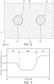
- FIG. 7 is a graph showing an impurity concentration profile, in which the horizontal axis is the position along line G-G' of FIG. 3B , and the vertical axis is the impurity concentration.
- a cell part Rc that carries current, a boundary part Ri that surrounds the cell part Rc, and a termination part Rt that surrounds the boundary part Ri are set in a semiconductor device 1 according to the embodiment.
- the semiconductor device 1 is formed of one chip.
- the cell part Rc is rectangular when viewed from above.
- the termination part Rt is a frame-shaped part forming the outer edge of the chip.
- the boundary part Ri is a frame-shaped part located between the cell part Rc and the termination part Rt.
- P-i-n diode regions R1 and a JBS (junction barrier Schottky) region R2 are set in the cell part Rc.
- the multiple pi-n diode regions R1 are arranged in a staggered configuration inside the JBS region R2 when viewed from above.
- each p-i-n diode region R1 has an octagonal island shape.
- the arrangement of the multiple p-i-n diode regions R1 is not limited to a staggered configuration; and the shape of each p-i-n diode region R1 is not limited to octagonal.
- An XYZ orthogonal coordinate system is employed for convenience of description in the specification hereinbelow.
- the direction of the shortest arrangement period of the p-i-n diode region R1 is taken as an "X-direction"; the direction from a cathode electrode 10 toward an anode electrode 50 described below is taken as a "Z-direction”; and a direction orthogonal to the X-direction and the Z-direction is taken as a "Y-direction".
- the direction that is from the cathode electrode 10 toward the anode electrode 50 also is called “up”, and the opposite direction also is called “down”; however, these expressions are for convenience and are independent of the direction of gravity.
- the semiconductor device 1 includes the cathode electrode 10, a semiconductor part 20, a contact electrode 30, a Schottky electrode 40, the anode electrode 50, and an insulating film 60.
- the semiconductor part 20 is located on the cathode electrode 10.
- the contact electrode 30 is located in the cell part Rc on the semiconductor part 20.
- the Schottky electrode 40 and the anode electrode 50 are located in the cell part Rc and the boundary part Ri on the semiconductor part 20.
- the insulating film 60 is located in the boundary part Ri and the termination part Rt on the semiconductor part 20.
- the insulating film 60 is located between the semiconductor part 20 and the Schottky electrode 40 in the boundary part Ri.
- the insulating film 60 is formed of silicon oxide (SiO 2 ).
- the Schottky electrode 40 and the anode electrode 50 are not illustrated in FIG. 1 .
- the semiconductor part 20 includes, for example, silicon carbide (SiC); and the conductivity type is set to an n-type or a p-type by introducing an impurity to each portion.
- the "n + -type” indicates a higher impurity concentration than the "n-type”; and the "n - -type” indicates a lower impurity concentration than the "n-type”. This is similar for the p-type as well.
- the "impurity concentration” refers to the effective concentration contributing to the conduction of the semiconductor, and refers to the concentration excluding the cancelled portion when one portion includes both an impurity that forms acceptors and an impurity that forms donors.
- the semiconductor part 20 includes an n + -type drain layer 21, an n - -type drift layer 22, an n + -type layer 23, a p-type layer 24, a p + -type layer 25, an n-type layer 26, a p-type layer 27, and a p - -type RESURF layer 28.
- the n + -type drain layer 21 and the n - -type drift layer 22 are located in both the p-i-n diode region R1 and the JBS region R2.
- the n + -type layer 23, the p-type layer 24, and the p + -type layer 25 are located in each p-i-n diode region R1.
- pluralities of the n + -type layer 23, the p-type layer 24, and the p + -type layer 25 are included, and each has, for example, an octagonal island shape when viewed from above.
- the n-type layer 26 and the p-type layer 27 are located in the JBS region R2.
- the p - -type RESURF layer 28 is located in the termination part Rt.
- the n + -type drain layer 21 is located on the entire cathode electrode 10 and contacts the cathode electrode 10.
- the conductivity type of the n + -type drain layer 21 is the n + -type.
- the n - -type drift layer 22 is located on the entire n + -type drain layer 21 and contacts the n + -type drain layer 21.
- the conductivity type of the n - -type drift layer 22 is the n - -type. In other words, the impurity concentration of the n - -type drift layer 22 is less than the impurity concentration of the n + -type drain layer 21.
- the n + -type layer 23 is located in the p-i-n diode region R1 on the n - -type drift layer 22.
- the n + -type layer 23 contacts the n - -type drift layer 22.
- the conductivity type of the n + -type layer 23 is the n + -type; and the impurity concentration of the n + -type layer 23 is greater than the impurity concentration of the n - -type drift layer 22.
- the p-type layer 24 is located in the p-i-n diode region R1 on the n + -type layer 23.
- the outer edge of each p-type layer 24 is slightly larger than the outer edge of each n + -type layer 23 when viewed from above.
- the outer perimeter portion of the p-type layer 24 is located on the n - -type drift layer 22; and the portion of the p-type layer 24 other than the outer perimeter portion is located on the n + -type layer 23.
- the p-type layer 24 contacts the n + -type layer 23 and the n - -type drift layer 22.
- the upper surface of the p-type layer 24 is exposed at the upper surface of the semiconductor part 20.
- the conductivity type of the p-type layer 24 is the p-type.
- the p + -type layer 25 is located on a portion of the p-type layer 24.
- the outer edge of the p + -type layer 25 is slightly smaller than the outer edge of the p-type layer 24 when viewed from above.
- the p + -type layer 25 is located in a region directly above the n + -type layer 23.
- the p + -type layer 25 contacts the p-type layer 24.
- the upper surface of the p + -type layer 25 is exposed at the upper surface of the semiconductor part 20.
- the impurity concentration of the p + -type layer 25 is greater than the impurity concentration of the p-type layer 24.
- a p-n diode is formed of the p-type part made of the p-type layer 24 and the p + -type layer 25 and the n-type part made of the n + -type drain layer 21, the n - -type drift layer 22, and the n + -type layer 23.
- the n-type layer 26 is located in the JBS region R2 on the n - -type drift layer 22.
- the n-type layer 26 contacts the n - -type drift layer 22.
- the n-type layer 26 may be in contact with or separated from the p-type layer 24.
- the n-type layer 26 is separated from the n + -type layer 23 with a portion 22a of the n - -type drift layer 22 interposed.
- the width of the portion 22a of the n - -type drift layer 22 in the X-direction i.e., the gap between the n-type layer 26 and the n + -type layer 23, is about 0.3 to 0.7 ⁇ m.
- the conductivity type of the n-type layer 26 is the n-type; and the impurity concentration of the n-type layer 26 is greater than the impurity concentration of the n - -type drift layer 22, less than the impurity concentration of the n + -type layer 23, and less than the impurity concentration of the n + -type drain layer 21.
- the impurity concentration of the n-type layer 26 is about 1 ⁇ 10 17 cm -3 ; the impurity concentration of the n + -type layer 23 is about 1 ⁇ 10 18 cm -3 ; and the impurity concentration of the n - -type drift layer 22 is about 1 ⁇ 10 16 cm -3 . Therefore, as shown in FIG. 7 , the impurity concentration profile along line G-G' shown in FIG. 3B has a minimum value in the n - -type drift layer 22.
- the p-type layer 27 is located on a portion of the n-type layer 26.
- the conductivity type of the p-type layer 27 is the p-type.
- Multiple p-type layers 27 are included and have stripe shapes extending in the Y-direction.
- the multiple p-type layers 27 are periodically arranged in the X-direction.
- a portion of the n-type layer 26 is located between the two p-type layers 27 next to each other in the X-direction.
- the lower surface of the p-type layer 27 is positioned higher than the lower surface of the n-type layer 26.
- the upper surface of the p-type layer 27 is exposed at the upper surface of the semiconductor part 20.
- the upper surface of the portion of the n-type layer 26 located between the p-type layers 27 also is exposed at the upper surface of the semiconductor part 20.
- the upper surfaces of the p-type layers 27 and the upper surface of the portion of the n-type layer 26 located between the p-type layers 27 are positioned in the same plane.
- multiple p-type layers 27 consecutively arranged along the X-direction are included in one group, and the Y-direction end portions of the multiple p-type layers 27 belonging to each group contact a common p-type layer 24.
- the multiple p-type layers 27 that belong to one group are located between two p-type layers 24 next to each other in the Y-direction.
- the multiple p-type layers 27 that belong to each group are located between two p-type layers 24 next to each other in the X-direction.
- the p - -type RESURF layer 28 is located in the termination part Rt on the n - -type drift layer 22.
- the p - -type RESURF layer 28 contacts the n - -type drift layer 22 and the p-type layer 24.
- the conductivity type of the p - -type RESURF layer 28 is the p - -type; and the impurity concentration of the p - -type RESURF layer 28 is less than the impurity concentration of the p-type layer 24.
- the contact electrode 30 is located in the p-i-n diode region R1 on the semiconductor part 20. Namely, in the semiconductor device 1, for example, the multiple contact electrodes 30 are arranged in a staggered configuration. For example, each contact electrode 30 is octagonal when viewed from above.
- the contact electrode 30 is located on the p + -type layer 25 and contacts the p + -type layer 25. Thereby, the contact electrode 30 has an ohmic connection with the p + -type layer 25.
- the Schottky electrode 40 is located in both the p-i-n diode region R1 and the JBS region R2 on the semiconductor part 20.
- the Schottky electrode 40 covers the multiple contact electrodes 30 and is connected with the multiple contact electrodes 30.
- the Schottky electrode 40 is located on the n-type layer 26 and on the p-type layer 27 and contacts the n-type layer 26 and the p-type layer 27.
- the Schottky electrode 40 forms a Schottky barrier diode together with the n-type layer 26.
- the Schottky electrode 40 has an ohmic connection with the p-type layer 27.
- the anode electrode 50 is located on the Schottky electrode 40 in the cell part Rc and the boundary part Ri.
- the anode electrode 50 contacts the Schottky electrode 40 and is connected to the Schottky electrode 40.
- FIG. 8 is a schematic cross-sectional view showing a normal operation of the semiconductor device according to the embodiment when forward-biased.
- FIG. 9 is a schematic cross-sectional view showing a normal operation of the semiconductor device according to the embodiment when reverse-biased.
- FIG. 10 is a schematic cross-sectional view showing when a reverse surge current flows in the semiconductor device according to the embodiment.
- FIGS. 8 and 10 the path of a current I is shown by a broken line.
- the forward current I flows in the Schottky barrier diode made of the Schottky electrode 40 and the n-type layer 26 in the JBS region R2.
- the forward current I flows in the n-type layer 26 of the JBS region R2.
- the resistance (the on-resistance) of the forward current can be reduced because the impurity concentration of the n-type layer 26 is greater than the impurity concentration of the n - -type drift layer 22.
- the position of the maximum electric field strength can be shifted into the semiconductor part 20 from the interface between the Schottky electrode 40 and the n-type layer 26. Because the interface between the Schottky electrode 40 and the n-type layer 26 has many defects, the leakage current when reverse-biased can be reduced by reducing the electric field strength at the interface.
- a large surge current may instantaneously flow in the semiconductor device 1 when the power supply connected to the semiconductor device 1 is switched on or off, when the load connected to the semiconductor device 1 fluctuates, etc.
- breakdown of the n + -type layer 23 of the p-i-n diode region R1 occurs, and a surge current flows in the p-n diode made of the p-type layer 24 and the n + -type layer 23.
- the greater part of the surge current can flow in the p-i-n diode region R1; and the JBS region R2 can be protected.
- thermal breakdown of the Schottky barrier diode made of the Schottky electrode 40 and the n-type layer 26 due to the surge current can be suppressed.
- the flow of a surge current between the n + -type layer 23 and the n-type layer 26 can be suppressed because the n-type layer 26 is separated from the n + -type layer 23.
- leakage of the surge current from the p-i-n diode region R1 into the JBS region R2 can be suppressed when the p-i-n diode region R1 carries the surge current; and the Schottky barrier diode can be more reliably protected from the surge current.
- the on-resistance can be reduced by providing the n-type layer 26 on the n - -type drift layer 22 in the JBS region R2. Also, by separating the n-type layer 26 from the n + -type layer 23, the flow of the surge current into the Schottky barrier diode can be suppressed, and thermal breakdown of the Schottky barrier diode can be suppressed.
- a semiconductor device can be realized in which the breakdown voltage for surge current can be improved.
Abstract
A semiconductor device includes a first electrode, a first semiconductor layer, a second semiconductor layer, a third semiconductor layer, a fourth semiconductor layer, a fifth semiconductor layer, and a second electrode. The fourth semiconductor layer is located in a second region on the first semiconductor layer. The fourth semiconductor layer is separated from the second semiconductor layer with a portion of the first semiconductor layer interposed. An impurity concentration of the fourth semiconductor layer is greater than an impurity concentration of the first semiconductor layer and less than an impurity concentration of the second semiconductor layer.
Description
- Embodiments relate to a semiconductor device.
- A Schottky barrier diode (SBD) realizes a diode by forming a junction between a metal and an n-type semiconductor and by utilizing the work function difference between the metal and the n-type semiconductor. To suppress leakage current, a junction barrier Schottky (JBS) structure also has been proposed, in which a p-type layer is located in a portion of the semiconductor at the junction surface with the metal, so that a depletion layer is formed with the p-n interface as a starting point when reverse-biased, thereby moving the position of the maximum electric field strength toward the semiconductor side from the junction interface between the metal and the semiconductor. It is desirable for such a semiconductor device to be more resistant to surge current.
-
-
FIG. 1 is a plan view showing a semiconductor device according to an embodiment; -
FIG. 2 is a cross-sectional view showing the semiconductor device according to the embodiment; -
FIG. 3A is a cross-sectional view along line A-A' shown inFIG. 1 ; andFIG. 3B is a partially enlarged cross-sectional view showing a region B ofFIG. 3A ; -
FIG. 4 is a cross-sectional view corresponding to a region C ofFIG. 1 and shows a position of line D-D' ofFIG. 3A ; -
FIG. 5 is a cross-sectional view corresponding to the region C ofFIG. 1 and shows a position of line E-E' ofFIG. 3A ; -
FIG. 6 is a cross-sectional view corresponding to the region C ofFIG. 1 and shows a position of line F-F' ofFIG. 3A ; -
FIG. 7 is a graph showing an impurity concentration profile, in which the horizontal axis is a position along line G-G' ofFIG. 3B , and the vertical axis is the impurity concentration; -
FIG. 8 is a schematic cross-sectional view showing a normal operation of the semiconductor device according to the embodiment when forward-biased; -
FIG. 9 is a schematic cross-sectional view showing a normal operation of the semiconductor device according to the embodiment when reverse-biased; and -
FIG. 10 is a schematic cross-sectional view showing when a reverse surge current flows in the semiconductor device according to the embodiment. - In general, according to one embodiment, a semiconductor device includes a first electrode, a first semiconductor layer, a second semiconductor layer, a third semiconductor layer, a fourth semiconductor layer, a fifth semiconductor layer, and a second electrode. The first semiconductor layer is connected to the first electrode. The first semiconductor layer is of a first conductivity type. The second semiconductor layer is located in a first region on the first semiconductor layer. The second semiconductor layer is of the first conductivity type. An impurity concentration of the second semiconductor layer is greater than an impurity concentration of the first semiconductor layer. The third semiconductor layer is located on the second semiconductor layer. The third semiconductor layer is of a second conductivity type. The fourth semiconductor layer is located in a second region on the first semiconductor layer. The fourth semiconductor layer is separated from the second semiconductor layer with a portion of the first semiconductor layer interposed. The fourth semiconductor layer is of the first conductivity type. An impurity concentration of the fourth semiconductor layer is greater than the impurity concentration of the first semiconductor layer and less than the impurity concentration of the second semiconductor layer. The fifth semiconductor layer is located on a portion of the fourth semiconductor layer. The fifth semiconductor layer is of the second conductivity type. The second electrode is connected to the third, fourth, and fifth semiconductor layers.
- An embodiment of the invention will now be described.
-
FIG. 1 is a plan view showing a semiconductor device according to the embodiment. -
FIG. 2 is a cross-sectional view showing the semiconductor device according to the embodiment. -
FIG. 3A is a cross-sectional view along line A-A' shown inFIG. 1 ; andFIG. 3B is a partially enlarged cross-sectional view showing region B ofFIG. 3A . -
FIG. 4 is a cross-sectional view corresponding to region C ofFIG. 1 and shows the position of line D-D' ofFIG. 3A . -
FIG. 5 is a cross-sectional view corresponding to region C ofFIG. 1 and shows the position of line E-E' ofFIG. 3A . -
FIG. 6 is a cross-sectional view corresponding to region C ofFIG. 1 and shows the position of line F-F' ofFIG. 3A . -
FIG. 7 is a graph showing an impurity concentration profile, in which the horizontal axis is the position along line G-G' ofFIG. 3B , and the vertical axis is the impurity concentration. - The drawings are schematic and are enhanced or simplified as appropriate. The dimensional ratios and numbers of components do not always match between the drawings.
- As shown in
FIGS. 1 and2 , a cell part Rc that carries current, a boundary part Ri that surrounds the cell part Rc, and a termination part Rt that surrounds the boundary part Ri are set in asemiconductor device 1 according to the embodiment. Thesemiconductor device 1 is formed of one chip. The cell part Rc is rectangular when viewed from above. The termination part Rt is a frame-shaped part forming the outer edge of the chip. The boundary part Ri is a frame-shaped part located between the cell part Rc and the termination part Rt. - P-i-n diode regions R1 and a JBS (junction barrier Schottky) region R2 are set in the cell part Rc. The multiple pi-n diode regions R1 are arranged in a staggered configuration inside the JBS region R2 when viewed from above. For example, each p-i-n diode region R1 has an octagonal island shape. The arrangement of the multiple p-i-n diode regions R1 is not limited to a staggered configuration; and the shape of each p-i-n diode region R1 is not limited to octagonal.
- An XYZ orthogonal coordinate system is employed for convenience of description in the specification hereinbelow. The direction of the shortest arrangement period of the p-i-n diode region R1 is taken as an "X-direction"; the direction from a
cathode electrode 10 toward ananode electrode 50 described below is taken as a "Z-direction"; and a direction orthogonal to the X-direction and the Z-direction is taken as a "Y-direction". Among the Z-directions, the direction that is from thecathode electrode 10 toward theanode electrode 50 also is called "up", and the opposite direction also is called "down"; however, these expressions are for convenience and are independent of the direction of gravity. - As shown in
FIGS. 1 to 6 , thesemiconductor device 1 includes thecathode electrode 10, asemiconductor part 20, acontact electrode 30, aSchottky electrode 40, theanode electrode 50, and an insulatingfilm 60. Thesemiconductor part 20 is located on thecathode electrode 10. Thecontact electrode 30 is located in the cell part Rc on thesemiconductor part 20. TheSchottky electrode 40 and theanode electrode 50 are located in the cell part Rc and the boundary part Ri on thesemiconductor part 20. The insulatingfilm 60 is located in the boundary part Ri and the termination part Rt on thesemiconductor part 20. The insulatingfilm 60 is located between thesemiconductor part 20 and theSchottky electrode 40 in the boundary part Ri. For example, the insulatingfilm 60 is formed of silicon oxide (SiO2). TheSchottky electrode 40 and theanode electrode 50 are not illustrated inFIG. 1 . - The
semiconductor part 20 includes, for example, silicon carbide (SiC); and the conductivity type is set to an n-type or a p-type by introducing an impurity to each portion. In the specification, the "n+-type" indicates a higher impurity concentration than the "n-type"; and the "n--type" indicates a lower impurity concentration than the "n-type". This is similar for the p-type as well. In the specification, the "impurity concentration" refers to the effective concentration contributing to the conduction of the semiconductor, and refers to the concentration excluding the cancelled portion when one portion includes both an impurity that forms acceptors and an impurity that forms donors. - The
semiconductor part 20 includes an n+-type drain layer 21, an n--type drift layer 22, an n+-type layer 23, a p-type layer 24, a p+-type layer 25, an n-type layer 26, a p-type layer 27, and a p--type RESURF layer 28. Among these layers, the n+-type drain layer 21 and the n--type drift layer 22 are located in both the p-i-n diode region R1 and the JBS region R2. The n+-type layer 23, the p-type layer 24, and the p+-type layer 25 are located in each p-i-n diode region R1. In other words, in thesemiconductor device 1, pluralities of the n+-type layer 23, the p-type layer 24, and the p+-type layer 25 are included, and each has, for example, an octagonal island shape when viewed from above. The n-type layer 26 and the p-type layer 27 are located in the JBS region R2. The p--type RESURF layer 28 is located in the termination part Rt. - The n+-
type drain layer 21 is located on theentire cathode electrode 10 and contacts thecathode electrode 10. The conductivity type of the n+-type drain layer 21 is the n+-type. The n--type drift layer 22 is located on the entire n+-type drain layer 21 and contacts the n+-type drain layer 21. The conductivity type of the n--type drift layer 22 is the n--type. In other words, the impurity concentration of the n--type drift layer 22 is less than the impurity concentration of the n+-type drain layer 21. - The n+-
type layer 23 is located in the p-i-n diode region R1 on the n--type drift layer 22. The n+-type layer 23 contacts the n--type drift layer 22. The conductivity type of the n+-type layer 23 is the n+-type; and the impurity concentration of the n+-type layer 23 is greater than the impurity concentration of the n--type drift layer 22. - The p-
type layer 24 is located in the p-i-n diode region R1 on the n+-type layer 23. The outer edge of each p-type layer 24 is slightly larger than the outer edge of each n+-type layer 23 when viewed from above. In other words, the outer perimeter portion of the p-type layer 24 is located on the n--type drift layer 22; and the portion of the p-type layer 24 other than the outer perimeter portion is located on the n+-type layer 23. The p-type layer 24 contacts the n+-type layer 23 and the n--type drift layer 22. The upper surface of the p-type layer 24 is exposed at the upper surface of thesemiconductor part 20. The conductivity type of the p-type layer 24 is the p-type. - The p+-
type layer 25 is located on a portion of the p-type layer 24. The outer edge of the p+-type layer 25 is slightly smaller than the outer edge of the p-type layer 24 when viewed from above. For example, the p+-type layer 25 is located in a region directly above the n+-type layer 23. The p+-type layer 25 contacts the p-type layer 24. The upper surface of the p+-type layer 25 is exposed at the upper surface of thesemiconductor part 20. The impurity concentration of the p+-type layer 25 is greater than the impurity concentration of the p-type layer 24. In the p-i-n diode region R1, a p-n diode is formed of the p-type part made of the p-type layer 24 and the p+-type layer 25 and the n-type part made of the n+-type drain layer 21, the n--type drift layer 22, and the n+-type layer 23. - The n-
type layer 26 is located in the JBS region R2 on the n--type drift layer 22. The n-type layer 26 contacts the n--type drift layer 22. The n-type layer 26 may be in contact with or separated from the p-type layer 24. The n-type layer 26 is separated from the n+-type layer 23 with aportion 22a of the n--type drift layer 22 interposed. For example, the width of theportion 22a of the n--type drift layer 22 in the X-direction, i.e., the gap between the n-type layer 26 and the n+-type layer 23, is about 0.3 to 0.7 µm. The conductivity type of the n-type layer 26 is the n-type; and the impurity concentration of the n-type layer 26 is greater than the impurity concentration of the n--type drift layer 22, less than the impurity concentration of the n+-type layer 23, and less than the impurity concentration of the n+-type drain layer 21. - For example, the impurity concentration of the n-
type layer 26 is about 1×1017 cm-3; the impurity concentration of the n+-type layer 23 is about 1×1018 cm-3; and the impurity concentration of the n--type drift layer 22 is about 1×1016 cm-3. Therefore, as shown inFIG. 7 , the impurity concentration profile along line G-G' shown inFIG. 3B has a minimum value in the n--type drift layer 22. - The p-
type layer 27 is located on a portion of the n-type layer 26. The conductivity type of the p-type layer 27 is the p-type. Multiple p-type layers 27 are included and have stripe shapes extending in the Y-direction. The multiple p-type layers 27 are periodically arranged in the X-direction. A portion of the n-type layer 26 is located between the two p-type layers 27 next to each other in the X-direction. The lower surface of the p-type layer 27 is positioned higher than the lower surface of the n-type layer 26. The upper surface of the p-type layer 27 is exposed at the upper surface of thesemiconductor part 20. The upper surface of the portion of the n-type layer 26 located between the p-type layers 27 also is exposed at the upper surface of thesemiconductor part 20. The upper surfaces of the p-type layers 27 and the upper surface of the portion of the n-type layer 26 located between the p-type layers 27 are positioned in the same plane. - In an example, multiple p-
type layers 27 consecutively arranged along the X-direction are included in one group, and the Y-direction end portions of the multiple p-type layers 27 belonging to each group contact a common p-type layer 24. Namely, the multiple p-type layers 27 that belong to one group are located between two p-type layers 24 next to each other in the Y-direction. Also, the multiple p-type layers 27 that belong to each group are located between two p-type layers 24 next to each other in the X-direction. - The p--
type RESURF layer 28 is located in the termination part Rt on the n--type drift layer 22. The p--type RESURF layer 28 contacts the n--type drift layer 22 and the p-type layer 24. The conductivity type of the p--type RESURF layer 28 is the p--type; and the impurity concentration of the p--type RESURF layer 28 is less than the impurity concentration of the p-type layer 24. - The
contact electrode 30 is located in the p-i-n diode region R1 on thesemiconductor part 20. Namely, in thesemiconductor device 1, for example, themultiple contact electrodes 30 are arranged in a staggered configuration. For example, eachcontact electrode 30 is octagonal when viewed from above. Thecontact electrode 30 is located on the p+-type layer 25 and contacts the p+-type layer 25. Thereby, thecontact electrode 30 has an ohmic connection with the p+-type layer 25. - The
Schottky electrode 40 is located in both the p-i-n diode region R1 and the JBS region R2 on thesemiconductor part 20. TheSchottky electrode 40 covers themultiple contact electrodes 30 and is connected with themultiple contact electrodes 30. In the JBS region R2, theSchottky electrode 40 is located on the n-type layer 26 and on the p-type layer 27 and contacts the n-type layer 26 and the p-type layer 27. TheSchottky electrode 40 forms a Schottky barrier diode together with the n-type layer 26. TheSchottky electrode 40 has an ohmic connection with the p-type layer 27. - The
anode electrode 50 is located on theSchottky electrode 40 in the cell part Rc and the boundary part Ri. Theanode electrode 50 contacts theSchottky electrode 40 and is connected to theSchottky electrode 40. - Operations of the
semiconductor device 1 according to the embodiment will now be described. -
FIG. 8 is a schematic cross-sectional view showing a normal operation of the semiconductor device according to the embodiment when forward-biased. -
FIG. 9 is a schematic cross-sectional view showing a normal operation of the semiconductor device according to the embodiment when reverse-biased. -
FIG. 10 is a schematic cross-sectional view showing when a reverse surge current flows in the semiconductor device according to the embodiment. - In
FIGS. 8 and10 , the path of a current I is shown by a broken line. - As shown in
FIG. 8 , when thesemiconductor device 1 is forward-biased, that is, when a voltage is applied so that theanode electrode 50 is positive and thecathode electrode 10 is negative, the forward current I flows in the Schottky barrier diode made of theSchottky electrode 40 and the n-type layer 26 in the JBS region R2. Thereby, the forward current I flows in the n-type layer 26 of the JBS region R2. At this time, the resistance (the on-resistance) of the forward current can be reduced because the impurity concentration of the n-type layer 26 is greater than the impurity concentration of the n--type drift layer 22. - As shown in
FIG. 9 , when thesemiconductor device 1 is reversed-biased, that is, when a voltage is applied so that theanode electrode 50 is negative and thecathode electrode 10 is positive, a depletion layer spreads inside thesemiconductor part 20 with the interface between theSchottky electrode 40 and the n-type layer 26, the interface between the p-type layer 27 and the n-type layer 26, and the interface between the p-type layer 24 and the n+-type layer 23 as starting points. The current is blocked thereby. - At this time, because the p-
type layer 27 is located in the JBS region R2, the position of the maximum electric field strength can be shifted into thesemiconductor part 20 from the interface between theSchottky electrode 40 and the n-type layer 26. Because the interface between theSchottky electrode 40 and the n-type layer 26 has many defects, the leakage current when reverse-biased can be reduced by reducing the electric field strength at the interface. - A large surge current may instantaneously flow in the
semiconductor device 1 when the power supply connected to thesemiconductor device 1 is switched on or off, when the load connected to thesemiconductor device 1 fluctuates, etc. In such a case, as shown inFIG. 10 , breakdown of the n+-type layer 23 of the p-i-n diode region R1 occurs, and a surge current flows in the p-n diode made of the p-type layer 24 and the n+-type layer 23. Thereby, the greater part of the surge current can flow in the p-i-n diode region R1; and the JBS region R2 can be protected. As a result, thermal breakdown of the Schottky barrier diode made of theSchottky electrode 40 and the n-type layer 26 due to the surge current can be suppressed. - In the
semiconductor device 1, the flow of a surge current between the n+-type layer 23 and the n-type layer 26 can be suppressed because the n-type layer 26 is separated from the n+-type layer 23. Thereby, leakage of the surge current from the p-i-n diode region R1 into the JBS region R2 can be suppressed when the p-i-n diode region R1 carries the surge current; and the Schottky barrier diode can be more reliably protected from the surge current. - Effects of the embodiment will now be described.
- In the
semiconductor device 1 as described above, the on-resistance can be reduced by providing the n-type layer 26 on the n--type drift layer 22 in the JBS region R2. Also, by separating the n-type layer 26 from the n+-type layer 23, the flow of the surge current into the Schottky barrier diode can be suppressed, and thermal breakdown of the Schottky barrier diode can be suppressed. - According to the embodiments described above, a semiconductor device can be realized in which the breakdown voltage for surge current can be improved.
- While certain embodiments have been described, these embodiments have been presented by way of example only, and are not intended to limit the scope of the inventions. Indeed, the novel embodiments described herein may be embodied in a variety of other forms; furthermore, various omissions, substitutions and changes in the form of the embodiments described herein may be made without departing from the spirit of the inventions. The accompanying claims and their equivalents are intended to cover such forms or modifications as would fall within the scope and spirit of the inventions.
- It is explicitly stated that all features disclosed in the description and/or the claims are intended to be disclosed separately and independently from each other for the purpose of original disclosure as well as for the purpose of restricting the claimed invention independent of the composition of the features in the embodiments and/or the claims. It is explicitly stated that all value ranges or indications of groups of entities disclose every possible intermediate value or intermediate entity for the purpose of original disclosure as well as for the purpose of restricting the claimed invention, in particular as limits of value ranges.
Claims (12)
- A semiconductor device (1), comprising:a first electrode (10);a first semiconductor layer (22) connected to the first electrode, the first semiconductor layer being of a first conductivity type (n);a second semiconductor layer (23) located in a first region (R1) on the first semiconductor layer, the second semiconductor layer being of the first conductivity type, an impurity concentration of the second semiconductor layer being greater than an impurity concentration of the first semiconductor layer;a third semiconductor layer (24+25) located on the second semiconductor layer, the third semiconductor layer being of a second conductivity type (p);a fourth semiconductor layer (26) located in a second region (R2) on the first semiconductor layer, the fourth semiconductor layer being separated from the second semiconductor layer with a portion of the first semiconductor layer interposed, the fourth semiconductor layer being of the first conductivity type, an impurity concentration of the fourth semiconductor layer being greater than the impurity concentration of the first semiconductor layer and less than the impurity concentration of the second semiconductor layer;a fifth semiconductor layer (27) located on a portion of the fourth semiconductor layer, the fifth semiconductor layer being of the second conductivity type; anda second electrode (30+40) connected to the third, fourth, and fifth semiconductor layers.
- The device according to claim 1, whereinthe third semiconductor layer is island-shaped when viewed from above, andthe fifth semiconductor layer is stripe-shaped when viewed from above.
- The device according to claim 1 or 2, wherein
the third semiconductor layer is octagonal island-shaped when viewed from above. - The device according to any of claims 1-3, whereina plurality of the third semiconductor layers is provided, andthe plurality of third semiconductor layers is arranged in a staggered configuration when viewed from above.
- The device according to any of claims 1-4, wherein
an outer edge of the third semiconductor layer is larger than an outer edge of the second semiconductor layer when viewed from above. - The device according to any of claims 1-5, wherein
the second semiconductor layer is in contact with the third semiconductor layer. - The device according to any of claims 1-6, wherein
the second semiconductor layer is separated from the fourth semiconductor layer with the first semiconductor layer interposed. - The device according to claim 7, wherein
a gap between the second semiconductor layer and the fourth semiconductor layer is not less than 0.3 µm and not more than 0.7 µm. - The device according to any of claims 1-8, further comprising:a sixth semiconductor layer (21) located between the first electrode and the first semiconductor layer,the sixth semiconductor layer being of the first conductivity type,an impurity concentration of the sixth semiconductor layer being greater than the impurity concentration of the first semiconductor layer.
- The device according to claim 9, wherein
the impurity concentration of the sixth semiconductor layer is greater than the impurity concentration of the fourth semiconductor layer. - The device according to any of claims 1-10, wherein
the second electrode includes:a third electrode (30) contacting the third semiconductor layer; anda fourth electrode (40) contacting the fourth and fifth semiconductor layers. - The device according to any of claims 1-11, wherein
the first semiconductor layer, the second semiconductor layer, the third semiconductor layer, the fourth semiconductor layer, and the fifth semiconductor layer include silicon and carbon.
Applications Claiming Priority (1)
| Application Number | Priority Date | Filing Date | Title |
|---|---|---|---|
| JP2022041425A JP2023136028A (en) | 2022-03-16 | 2022-03-16 | Semiconductor device |
Publications (1)
| Publication Number | Publication Date |
|---|---|
| EP4246585A1 true EP4246585A1 (en) | 2023-09-20 |
Family
ID=82786631
Family Applications (1)
| Application Number | Title | Priority Date | Filing Date |
|---|---|---|---|
| EP22188249.1A Pending EP4246585A1 (en) | 2022-03-16 | 2022-08-02 | Semiconductor device |
Country Status (4)
| Country | Link |
|---|---|
| US (1) | US20230299211A1 (en) |
| EP (1) | EP4246585A1 (en) |
| JP (1) | JP2023136028A (en) |
| CN (1) | CN116799003A (en) |
Citations (4)
| Publication number | Priority date | Publication date | Assignee | Title |
|---|---|---|---|---|
| US20130140584A1 (en) * | 2010-06-02 | 2013-06-06 | Norifumi Kameshiro | Semiconductor device |
| US20200091298A1 (en) * | 2018-09-19 | 2020-03-19 | Kabushiki Kaisha Toshiba | Semiconductor device |
| US20210305435A1 (en) * | 2020-03-24 | 2021-09-30 | Kabushiki Kaisha Toshiba | Semiconductor device |
| US20210376168A1 (en) * | 2020-05-29 | 2021-12-02 | Kabushiki Kaisha Toshiba | Semiconductor device |
-
2022
- 2022-03-16 JP JP2022041425A patent/JP2023136028A/en active Pending
- 2022-07-18 CN CN202210841233.9A patent/CN116799003A/en active Pending
- 2022-08-02 EP EP22188249.1A patent/EP4246585A1/en active Pending
- 2022-08-04 US US17/881,089 patent/US20230299211A1/en active Pending
Patent Citations (4)
| Publication number | Priority date | Publication date | Assignee | Title |
|---|---|---|---|---|
| US20130140584A1 (en) * | 2010-06-02 | 2013-06-06 | Norifumi Kameshiro | Semiconductor device |
| US20200091298A1 (en) * | 2018-09-19 | 2020-03-19 | Kabushiki Kaisha Toshiba | Semiconductor device |
| US20210305435A1 (en) * | 2020-03-24 | 2021-09-30 | Kabushiki Kaisha Toshiba | Semiconductor device |
| US20210376168A1 (en) * | 2020-05-29 | 2021-12-02 | Kabushiki Kaisha Toshiba | Semiconductor device |
Also Published As
| Publication number | Publication date |
|---|---|
| US20230299211A1 (en) | 2023-09-21 |
| CN116799003A (en) | 2023-09-22 |
| JP2023136028A (en) | 2023-09-29 |
Similar Documents
| Publication | Publication Date | Title |
|---|---|---|
| US9659927B2 (en) | Junction barrier Schottky rectifier | |
| US9147758B2 (en) | Semiconductor device | |
| US10566464B2 (en) | Semiconductor device | |
| US8937319B2 (en) | Schottky barrier diode | |
| JP5863574B2 (en) | Semiconductor device | |
| JP2011199223A (en) | Semiconductor device | |
| JP7305591B2 (en) | semiconductor equipment | |
| US20190035944A1 (en) | Schottky diode | |
| JP2024019673A (en) | semiconductor equipment | |
| CN109524458B (en) | Semiconductor device with a plurality of semiconductor chips | |
| US20210013309A1 (en) | Silicon carbide semiconductor device | |
| EP4246585A1 (en) | Semiconductor device | |
| CN116646406A (en) | Wide band gap semiconductor device and method of manufacturing the same | |
| US20220376073A1 (en) | Schottky barrier diode | |
| EP4343848A1 (en) | Semiconductor device | |
| US11322585B2 (en) | Semiconductor device | |
| CN114335146B (en) | Semiconductor structure and preparation method thereof | |
| JP7237772B2 (en) | semiconductor equipment | |
| CN117410311A (en) | Semiconductor device with a semiconductor device having a plurality of semiconductor chips | |
| JP4863430B2 (en) | Surge protection semiconductor device | |
| CN105575962A (en) | Single-piece type hybrid rectifier diode structure |
Legal Events
| Date | Code | Title | Description |
|---|---|---|---|
| PUAI | Public reference made under article 153(3) epc to a published international application that has entered the european phase |
Free format text: ORIGINAL CODE: 0009012 |
|
| STAA | Information on the status of an ep patent application or granted ep patent |
Free format text: STATUS: REQUEST FOR EXAMINATION WAS MADE |
|
| 17P | Request for examination filed |
Effective date: 20220802 |
|
| AK | Designated contracting states |
Kind code of ref document: A1 Designated state(s): AL AT BE BG CH CY CZ DE DK EE ES FI FR GB GR HR HU IE IS IT LI LT LU LV MC MK MT NL NO PL PT RO RS SE SI SK SM TR |