EP4246571A1 - Semiconductor device and method for producing said semiconductor device - Google Patents
Semiconductor device and method for producing said semiconductor device Download PDFInfo
- Publication number
- EP4246571A1 EP4246571A1 EP22190766.0A EP22190766A EP4246571A1 EP 4246571 A1 EP4246571 A1 EP 4246571A1 EP 22190766 A EP22190766 A EP 22190766A EP 4246571 A1 EP4246571 A1 EP 4246571A1
- Authority
- EP
- European Patent Office
- Prior art keywords
- metal layer
- semiconductor device
- bond portion
- wall surface
- bonding wire
- Prior art date
- Legal status (The legal status is an assumption and is not a legal conclusion. Google has not performed a legal analysis and makes no representation as to the accuracy of the status listed.)
- Pending
Links
Images






Classifications
-
- H—ELECTRICITY
- H10—SEMICONDUCTOR DEVICES; ELECTRIC SOLID-STATE DEVICES NOT OTHERWISE PROVIDED FOR
- H10W—GENERIC PACKAGES, INTERCONNECTIONS, CONNECTORS OR OTHER CONSTRUCTIONAL DETAILS OF DEVICES COVERED BY CLASS H10
- H10W72/00—Interconnections or connectors in packages
- H10W72/071—Connecting or disconnecting
- H10W72/075—Connecting or disconnecting of bond wires
-
- H—ELECTRICITY
- H10—SEMICONDUCTOR DEVICES; ELECTRIC SOLID-STATE DEVICES NOT OTHERWISE PROVIDED FOR
- H10P—GENERIC PROCESSES OR APPARATUS FOR THE MANUFACTURE OR TREATMENT OF DEVICES COVERED BY CLASS H10
- H10P72/00—Handling or holding of wafers, substrates or devices during manufacture or treatment thereof
- H10P72/04—Apparatus for manufacture or treatment
- H10P72/0444—Apparatus for wiring semiconductor or solid-state device
-
- H—ELECTRICITY
- H10—SEMICONDUCTOR DEVICES; ELECTRIC SOLID-STATE DEVICES NOT OTHERWISE PROVIDED FOR
- H10W—GENERIC PACKAGES, INTERCONNECTIONS, CONNECTORS OR OTHER CONSTRUCTIONAL DETAILS OF DEVICES COVERED BY CLASS H10
- H10W40/00—Arrangements for thermal protection or thermal control
- H10W40/20—Arrangements for cooling
- H10W40/25—Arrangements for cooling characterised by their materials
- H10W40/255—Arrangements for cooling characterised by their materials having a laminate or multilayered structure, e.g. direct bond copper [DBC] ceramic substrates
-
- H—ELECTRICITY
- H10—SEMICONDUCTOR DEVICES; ELECTRIC SOLID-STATE DEVICES NOT OTHERWISE PROVIDED FOR
- H10W—GENERIC PACKAGES, INTERCONNECTIONS, CONNECTORS OR OTHER CONSTRUCTIONAL DETAILS OF DEVICES COVERED BY CLASS H10
- H10W72/00—Interconnections or connectors in packages
- H10W72/01—Manufacture or treatment
- H10W72/011—Apparatus therefor
- H10W72/0115—Apparatus for manufacturing bond wires
-
- H—ELECTRICITY
- H10—SEMICONDUCTOR DEVICES; ELECTRIC SOLID-STATE DEVICES NOT OTHERWISE PROVIDED FOR
- H10W—GENERIC PACKAGES, INTERCONNECTIONS, CONNECTORS OR OTHER CONSTRUCTIONAL DETAILS OF DEVICES COVERED BY CLASS H10
- H10W76/00—Containers; Fillings or auxiliary members therefor; Seals
- H10W76/01—Manufacture or treatment
-
- H—ELECTRICITY
- H10—SEMICONDUCTOR DEVICES; ELECTRIC SOLID-STATE DEVICES NOT OTHERWISE PROVIDED FOR
- H10W—GENERIC PACKAGES, INTERCONNECTIONS, CONNECTORS OR OTHER CONSTRUCTIONAL DETAILS OF DEVICES COVERED BY CLASS H10
- H10W76/00—Containers; Fillings or auxiliary members therefor; Seals
- H10W76/10—Containers or parts thereof
- H10W76/12—Containers or parts thereof characterised by their shape
- H10W76/13—Containers comprising a conductive base serving as an interconnection
- H10W76/134—Containers comprising a conductive base serving as an interconnection having other interconnections parallel to the conductive base
-
- H—ELECTRICITY
- H10—SEMICONDUCTOR DEVICES; ELECTRIC SOLID-STATE DEVICES NOT OTHERWISE PROVIDED FOR
- H10W—GENERIC PACKAGES, INTERCONNECTIONS, CONNECTORS OR OTHER CONSTRUCTIONAL DETAILS OF DEVICES COVERED BY CLASS H10
- H10W76/00—Containers; Fillings or auxiliary members therefor; Seals
- H10W76/40—Fillings or auxiliary members in containers, e.g. centering rings
- H10W76/42—Fillings
- H10W76/47—Solid or gel fillings
-
- H—ELECTRICITY
- H10—SEMICONDUCTOR DEVICES; ELECTRIC SOLID-STATE DEVICES NOT OTHERWISE PROVIDED FOR
- H10W—GENERIC PACKAGES, INTERCONNECTIONS, CONNECTORS OR OTHER CONSTRUCTIONAL DETAILS OF DEVICES COVERED BY CLASS H10
- H10W72/00—Interconnections or connectors in packages
- H10W72/01—Manufacture or treatment
- H10W72/011—Apparatus therefor
- H10W72/0116—Apparatus for manufacturing strap connectors
-
- H—ELECTRICITY
- H10—SEMICONDUCTOR DEVICES; ELECTRIC SOLID-STATE DEVICES NOT OTHERWISE PROVIDED FOR
- H10W—GENERIC PACKAGES, INTERCONNECTIONS, CONNECTORS OR OTHER CONSTRUCTIONAL DETAILS OF DEVICES COVERED BY CLASS H10
- H10W72/00—Interconnections or connectors in packages
- H10W72/01—Manufacture or treatment
- H10W72/015—Manufacture or treatment of bond wires
-
- H—ELECTRICITY
- H10—SEMICONDUCTOR DEVICES; ELECTRIC SOLID-STATE DEVICES NOT OTHERWISE PROVIDED FOR
- H10W—GENERIC PACKAGES, INTERCONNECTIONS, CONNECTORS OR OTHER CONSTRUCTIONAL DETAILS OF DEVICES COVERED BY CLASS H10
- H10W72/00—Interconnections or connectors in packages
- H10W72/071—Connecting or disconnecting
- H10W72/073—Connecting or disconnecting of die-attach connectors
-
- H—ELECTRICITY
- H10—SEMICONDUCTOR DEVICES; ELECTRIC SOLID-STATE DEVICES NOT OTHERWISE PROVIDED FOR
- H10W—GENERIC PACKAGES, INTERCONNECTIONS, CONNECTORS OR OTHER CONSTRUCTIONAL DETAILS OF DEVICES COVERED BY CLASS H10
- H10W72/00—Interconnections or connectors in packages
- H10W72/071—Connecting or disconnecting
- H10W72/075—Connecting or disconnecting of bond wires
- H10W72/07531—Techniques
- H10W72/07532—Compression bonding, e.g. thermocompression bonding
- H10W72/07533—Ultrasonic bonding, e.g. thermosonic bonding
-
- H—ELECTRICITY
- H10—SEMICONDUCTOR DEVICES; ELECTRIC SOLID-STATE DEVICES NOT OTHERWISE PROVIDED FOR
- H10W—GENERIC PACKAGES, INTERCONNECTIONS, CONNECTORS OR OTHER CONSTRUCTIONAL DETAILS OF DEVICES COVERED BY CLASS H10
- H10W72/00—Interconnections or connectors in packages
- H10W72/50—Bond wires
- H10W72/531—Shapes of wire connectors
- H10W72/5363—Shapes of wire connectors the connected ends being wedge-shaped
-
- H—ELECTRICITY
- H10—SEMICONDUCTOR DEVICES; ELECTRIC SOLID-STATE DEVICES NOT OTHERWISE PROVIDED FOR
- H10W—GENERIC PACKAGES, INTERCONNECTIONS, CONNECTORS OR OTHER CONSTRUCTIONAL DETAILS OF DEVICES COVERED BY CLASS H10
- H10W72/00—Interconnections or connectors in packages
- H10W72/50—Bond wires
- H10W72/531—Shapes of wire connectors
- H10W72/5366—Shapes of wire connectors the bond wires having kinks
-
- H—ELECTRICITY
- H10—SEMICONDUCTOR DEVICES; ELECTRIC SOLID-STATE DEVICES NOT OTHERWISE PROVIDED FOR
- H10W—GENERIC PACKAGES, INTERCONNECTIONS, CONNECTORS OR OTHER CONSTRUCTIONAL DETAILS OF DEVICES COVERED BY CLASS H10
- H10W72/00—Interconnections or connectors in packages
- H10W72/50—Bond wires
- H10W72/541—Dispositions of bond wires
-
- H—ELECTRICITY
- H10—SEMICONDUCTOR DEVICES; ELECTRIC SOLID-STATE DEVICES NOT OTHERWISE PROVIDED FOR
- H10W—GENERIC PACKAGES, INTERCONNECTIONS, CONNECTORS OR OTHER CONSTRUCTIONAL DETAILS OF DEVICES COVERED BY CLASS H10
- H10W72/00—Interconnections or connectors in packages
- H10W72/50—Bond wires
- H10W72/551—Materials of bond wires
- H10W72/552—Materials of bond wires comprising metals or metalloids, e.g. silver
- H10W72/5522—Materials of bond wires comprising metals or metalloids, e.g. silver comprising gold [Au]
-
- H—ELECTRICITY
- H10—SEMICONDUCTOR DEVICES; ELECTRIC SOLID-STATE DEVICES NOT OTHERWISE PROVIDED FOR
- H10W—GENERIC PACKAGES, INTERCONNECTIONS, CONNECTORS OR OTHER CONSTRUCTIONAL DETAILS OF DEVICES COVERED BY CLASS H10
- H10W72/00—Interconnections or connectors in packages
- H10W72/50—Bond wires
- H10W72/551—Materials of bond wires
- H10W72/552—Materials of bond wires comprising metals or metalloids, e.g. silver
- H10W72/5524—Materials of bond wires comprising metals or metalloids, e.g. silver comprising aluminium [Al]
-
- H—ELECTRICITY
- H10—SEMICONDUCTOR DEVICES; ELECTRIC SOLID-STATE DEVICES NOT OTHERWISE PROVIDED FOR
- H10W—GENERIC PACKAGES, INTERCONNECTIONS, CONNECTORS OR OTHER CONSTRUCTIONAL DETAILS OF DEVICES COVERED BY CLASS H10
- H10W72/00—Interconnections or connectors in packages
- H10W72/50—Bond wires
- H10W72/551—Materials of bond wires
- H10W72/552—Materials of bond wires comprising metals or metalloids, e.g. silver
- H10W72/5525—Materials of bond wires comprising metals or metalloids, e.g. silver comprising copper [Cu]
-
- H—ELECTRICITY
- H10—SEMICONDUCTOR DEVICES; ELECTRIC SOLID-STATE DEVICES NOT OTHERWISE PROVIDED FOR
- H10W—GENERIC PACKAGES, INTERCONNECTIONS, CONNECTORS OR OTHER CONSTRUCTIONAL DETAILS OF DEVICES COVERED BY CLASS H10
- H10W72/00—Interconnections or connectors in packages
- H10W72/851—Dispositions of multiple connectors or interconnections
- H10W72/874—On different surfaces
- H10W72/884—Die-attach connectors and bond wires
-
- H—ELECTRICITY
- H10—SEMICONDUCTOR DEVICES; ELECTRIC SOLID-STATE DEVICES NOT OTHERWISE PROVIDED FOR
- H10W—GENERIC PACKAGES, INTERCONNECTIONS, CONNECTORS OR OTHER CONSTRUCTIONAL DETAILS OF DEVICES COVERED BY CLASS H10
- H10W72/00—Interconnections or connectors in packages
- H10W72/90—Bond pads, in general
- H10W72/921—Structures or relative sizes of bond pads
- H10W72/926—Multiple bond pads having different sizes
-
- H—ELECTRICITY
- H10—SEMICONDUCTOR DEVICES; ELECTRIC SOLID-STATE DEVICES NOT OTHERWISE PROVIDED FOR
- H10W—GENERIC PACKAGES, INTERCONNECTIONS, CONNECTORS OR OTHER CONSTRUCTIONAL DETAILS OF DEVICES COVERED BY CLASS H10
- H10W74/00—Encapsulations, e.g. protective coatings
-
- H—ELECTRICITY
- H10—SEMICONDUCTOR DEVICES; ELECTRIC SOLID-STATE DEVICES NOT OTHERWISE PROVIDED FOR
- H10W—GENERIC PACKAGES, INTERCONNECTIONS, CONNECTORS OR OTHER CONSTRUCTIONAL DETAILS OF DEVICES COVERED BY CLASS H10
- H10W76/00—Containers; Fillings or auxiliary members therefor; Seals
- H10W76/10—Containers or parts thereof
- H10W76/12—Containers or parts thereof characterised by their shape
-
- H—ELECTRICITY
- H10—SEMICONDUCTOR DEVICES; ELECTRIC SOLID-STATE DEVICES NOT OTHERWISE PROVIDED FOR
- H10W—GENERIC PACKAGES, INTERCONNECTIONS, CONNECTORS OR OTHER CONSTRUCTIONAL DETAILS OF DEVICES COVERED BY CLASS H10
- H10W76/00—Containers; Fillings or auxiliary members therefor; Seals
- H10W76/10—Containers or parts thereof
- H10W76/12—Containers or parts thereof characterised by their shape
- H10W76/15—Containers comprising an insulating or insulated base
-
- H—ELECTRICITY
- H10—SEMICONDUCTOR DEVICES; ELECTRIC SOLID-STATE DEVICES NOT OTHERWISE PROVIDED FOR
- H10W—GENERIC PACKAGES, INTERCONNECTIONS, CONNECTORS OR OTHER CONSTRUCTIONAL DETAILS OF DEVICES COVERED BY CLASS H10
- H10W90/00—Package configurations
-
- H—ELECTRICITY
- H10—SEMICONDUCTOR DEVICES; ELECTRIC SOLID-STATE DEVICES NOT OTHERWISE PROVIDED FOR
- H10W—GENERIC PACKAGES, INTERCONNECTIONS, CONNECTORS OR OTHER CONSTRUCTIONAL DETAILS OF DEVICES COVERED BY CLASS H10
- H10W90/00—Package configurations
- H10W90/701—Package configurations characterised by the relative positions of pads or connectors relative to package parts
- H10W90/731—Package configurations characterised by the relative positions of pads or connectors relative to package parts of die-attach connectors
- H10W90/734—Package configurations characterised by the relative positions of pads or connectors relative to package parts of die-attach connectors between a chip and a stacked insulating package substrate, interposer or RDL
-
- H—ELECTRICITY
- H10—SEMICONDUCTOR DEVICES; ELECTRIC SOLID-STATE DEVICES NOT OTHERWISE PROVIDED FOR
- H10W—GENERIC PACKAGES, INTERCONNECTIONS, CONNECTORS OR OTHER CONSTRUCTIONAL DETAILS OF DEVICES COVERED BY CLASS H10
- H10W90/00—Package configurations
- H10W90/701—Package configurations characterised by the relative positions of pads or connectors relative to package parts
- H10W90/751—Package configurations characterised by the relative positions of pads or connectors relative to package parts of bond wires
- H10W90/754—Package configurations characterised by the relative positions of pads or connectors relative to package parts of bond wires between a chip and a stacked insulating package substrate, interposer or RDL
Definitions
- Embodiments described herein relate generally to a semiconductor device and a method for producing the semiconductor device.
- a power semiconductor chip is mounted on a metal base with an insulating substrate interposed between the power semiconductor chip and the metal base.
- the power semiconductor chip is, for example, a metal oxide semiconductor field effect transistor (MOSFET), an insulated gate bipolar transistor (IGBT), or a diode.
- MOSFET metal oxide semiconductor field effect transistor
- IGBT insulated gate bipolar transistor
- a semiconductor device includes: a frame body having a wall surface; an insulating substrate surrounded by the frame body, the insulating substrate having a first metal layer and a second metal layer on a surface, the second metal layer being located between the first metal layer and the wall surface; a semiconductor chip including an electrode and provided on the first metal layer; and a bonding wire having a first bond portion connected to the electrode, a second bond portion connected to the second metal layer, and an intermediate portion between the first bond portion and the second bond portion; wherein a second angle formed between a second direction in which the second bond portion extends and the wall surface is smaller than a first angle formed between a first direction in which the intermediate portion extends and the wall surface.
- a semiconductor device includes: a frame body having a wall surface; an insulating substrate surrounded by the frame body, the insulating substrate having a first metal layer and a second metal layer on a surface, the second metal layer being located between the first metal layer and the wall surface; a semiconductor chip including an electrode and provided on the first metal layer; and a bonding wire having a first bond portion connected to the electrode, a second bond portion connected to the second metal layer, and an intermediate portion between the first bond portion and the second bond portion.
- a second angle formed between a second direction in which the second bond portion extends and the wall surface is smaller than a first angle formed between a first direction in which the intermediate portion extends and the wall surface.
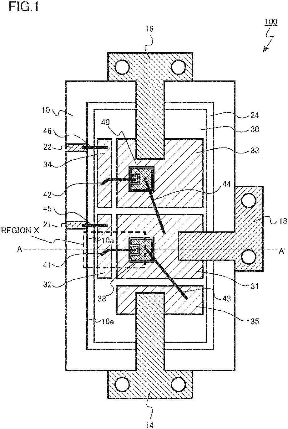
- FIG. 1 is a schematic top view of the semiconductor device according to the embodiment.
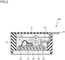
- FIG. 2 is a schematic cross-sectional view of the semiconductor device according to the embodiment.
- FIG. 2 is a cross section taken along line AA' in FIG. 1 .
- the semiconductor device of the embodiment is a power semiconductor module 100. As illustrated in FIG. 1 , in the power semiconductor module 100 of the embodiment, two MOSFETs are connected in series.
- the power semiconductor module of the embodiment is a so-called "two-in-one" module in which a half bridge circuit can be configured by one module. For example, a three-phase inverter circuit can be configured by using three power semiconductor modules of the embodiment.
- the power semiconductor module 100 of the embodiment includes a resin case 10 (frame body), a lid 12, a first main terminal 14, a second main terminal 16, an AC output terminal 18, a first gate terminal 21, a second gate terminal 22, a metal base 24, an insulating substrate 30, a first metal layer 31, a second metal layer 32, a third metal layer 33, a fourth metal layer 34, a fifth metal layer 35, a backside metal layer 36, a first MOSFET 38 (semiconductor chip), a second MOSFET 40, a first bonding wire 41 (bonding wire), a second bonding wire 42, a third bonding wire 43, a fourth bonding wire 44, a fifth bonding wire 45, a sixth bonding wire 46, and a sealing resin 50.
- the resin case 10 has a wall surface 10a.
- the first MOSFET 38 includes a gate electrode pad 38a (electrode), a source electrode 38b, a semiconductor layer 38c, and a drain electrode 38d.
- the first bonding wire 41 includes a first bond portion 41a, a second bond portion 41b, and a loop portion 41c.
- the loop portion 41c is an example of an intermediate portion.
- FIG. 1 is a top view of the power semiconductor module 100 from which the lid 12 and the sealing resin 50 are removed.
- the metal base 24 is made of, for example, copper.
- a heat sink (not illustrated) is connected to the back surface of the metal base 24.
- the insulating substrate 30 is provided above the metal base 24.
- the insulating substrate 30 is surrounded by the resin case 10.
- the insulating substrate 30 is provided between the metal base 24 and the first MOSFET 38 and between the metal base 24 and the second MOSFET 40.
- the insulating substrate 30 has a function of electrically separating the metal base 24 from the first MOSFET 38 and the second MOSFET 40.
- the insulating substrate 30 is made of, for example, ceramic.
- the insulating substrate 30 is made of, for example, aluminum oxide, aluminum nitride, or silicon nitride.
- the first metal layer 31, the second metal layer 32, the third metal layer 33, the fourth metal layer 34, and the fifth metal layer 35 are provided on the surface of the insulating substrate 30.
- the first metal layer 31, the second metal layer 32, the third metal layer 33, the fourth metal layer 34, and the fifth metal layer 35 are made of, for example, copper.
- the second metal layer 32 is located between the first metal layer 31 and the wall surface 10a of the resin case 10.
- the fourth metal layer 34 is located between the third metal layer 33 and the wall surface 10a of the resin case 10.
- the backside metal layer 36 is provided on the back surface of the insulating substrate 30.
- the backside metal layer 36 is made of, for example, copper.
- the backside metal layer 36 is bonded to the metal base 24 by using, for example, a solder layer or a metal nanoparticle layer (not illustrated).
- the resin case 10 is provided around the metal base 24 and the insulating substrate 30. A part of the resin case 10 is provided on the metal base 24.
- the resin case 10 is an example of a frame body.
- the resin case 10 has a function of protecting the first MOSFET 38, the second MOSFET 40, and the insulating substrate 30.
- the resin case 10 has a wall surface 10a.
- the lid 12 is provided on the resin case 10.
- the first MOSFET 38 and the second MOSFET 40 are disposed between the lid 12 and the insulating substrate 30.
- the lid 12 has a function of protecting the first MOSFET 38, the second MOSFET 40, and the insulating substrate 30.
- the first bonding wire 41, the second bonding wire 42, the third bonding wire 43, the fourth bonding wire 44, the fifth bonding wire 45, and the sixth bonding wire 46 electrically connect the members of the power semiconductor module 100.
- Materials of the first bonding wire 41, the second bonding wire 42, the third bonding wire 43, the fourth bonding wire 44, the fifth bonding wire 45, and the sixth bonding wire 46 are, for example, aluminum, copper, or gold.
- the first MOSFET 38 is provided above the insulating substrate 30.
- the first MOSFET 38 has the gate electrode pad 38a, the source electrode 38b, the semiconductor layer 38c, and the drain electrode 38d.
- the gate electrode pad 38a is an example of an electrode.
- the first MOSFET 38 is formed using, for example, silicon carbide.
- the semiconductor layer 38c is, for example, a silicon carbide layer.
- the first MOSFET 38 is provided on the first metal layer 31.
- the drain electrode 38d is fixed on the first metal layer 31 by using, for example, a solder layer or a metal nanoparticle layer (not illustrated).
- the drain electrode 38d is bonded to the first metal layer 31.
- the drain electrode 38d is electrically connected to the first metal layer 31.
- the source electrode 38b is electrically connected to the fifth metal layer 35.
- the source electrode 38b is electrically connected to the fifth metal layer 35 by the third bonding wire 43.
- the gate electrode pad 38a is electrically connected to the second metal layer 32.
- the gate electrode pad 38a is electrically connected to the second metal layer 32 by the first bonding wire 41.
- the second MOSFET 40 is provided above the insulating substrate 30.
- the second MOSFET 40 is provided on the third metal layer 33.
- the sealing resin 50 is filled in the resin case 10.
- the sealing resin 50 is surrounded by the resin case 10.
- the sealing resin 50 covers the first MOSFET 38, the second MOSFET 40, and the insulating substrate 30.
- the sealing resin 50 has a function of protecting the first MOSFET 38, the second MOSFET 40, and the insulating substrate 30. In addition, the sealing resin 50 has a function of insulating the first MOSFET 38, the second MOSFET 40, and the insulating substrate 30.
- the sealing resin 50 contains a resin.
- the sealing resin 50 is, for example, a silicone gel.
- other resins such as an epoxy resin and a polyimide resin can be applied to the sealing resin 50.
- the first main terminal 14 is electrically connected to the fifth metal layer 35. For example, a negative voltage is applied to the first main terminal 14 from the outside.
- the first main terminal 14 is made of, for example, copper.
- the second main terminal 16 is electrically connected to the third metal layer 33. For example, a positive voltage is applied to the second main terminal 16 from the outside.
- the second main terminal 16 is made of, for example, copper.
- the AC output terminal 18 is electrically connected to the first metal layer 31. One end of the AC output terminal 18 is fixed to the first metal layer 31, for example. The AC output terminal 18 outputs an output current of the half bridge circuit.
- the first gate terminal 21 is electrically connected to the gate electrode pad 38a of the first MOSFET 38.
- the first gate terminal 21 has a function of applying a gate voltage signal for controlling the first MOSFET 38 to the gate electrode pad 38a.
- the second gate terminal 22 is electrically connected to the gate electrode pad of the second MOSFET 40.
- the second gate terminal 22 has a function of applying a gate voltage signal for controlling the second MOSFET 40 to the gate electrode pad.
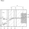
- FIG. 3 is an enlarged schematic top view of the semiconductor device according to the embodiment.
- FIG. 3 is an enlarged view of a region X surrounded by a broken line in FIG. 1 .
- FIG. 3 is a top view of a state in which the lid 12 and the sealing resin 50 are removed.
- FIG. 4 is an enlarged schematic cross-sectional view of the semiconductor device according to the embodiment.
- FIG. 4 is a cross-sectional view including a region along the bonding wire of FIG. 3 .
- the first bonding wire 41 has the first bond portion 41a, the second bond portion 41b, and the loop portion 41c.
- the first bond portion 41a is connected to the gate electrode pad 38a of the first MOSFET 38.
- the second bond portion 41b is connected to the second metal layer 32.
- the loop portion 41c is located between the first bond portion 41a and the second bond portion 41b.
- the first bond portion 41a is formed before the second bond portion 41b.
- the loop portion 41c extends in the first direction.
- An angle formed between the first direction and the wall surface 10a of the resin case 10 is a first angle ( ⁇ )1 in FIG. 3 ).
- the first angle ⁇ 1 is, for example, 60 degrees or more and 90 degrees or less.
- the second bond portion 41b extends in the second direction.
- the second direction is different from the first direction.
- An angle formed between the second direction and the wall surface 10a of the resin case 10 is a second angle ( ⁇ 2 in FIG. 3 ).
- the second angle is, for example, 0 degrees or more and 80 degrees or less.
- the second angle ⁇ 2 is smaller than the first angle ⁇ 1.
- the difference between the first angle ⁇ 1 and the second angle ⁇ 2 is, for example, 10 degrees or more and 90 degrees or less.
- the difference between the first angle ⁇ 1 and the second angle ⁇ 2 is preferably, for example, 20 degrees or more and 45 degrees or less.
- a method for producing a semiconductor device includes: preparing an insulating substrate surrounded by a frame body having a wall surface, the insulating substrate having a first metal layer and a second metal layer on a surface, the second metal layer being located between the first metal layer and the wall surface; disposing a semiconductor chip including an electrode on the first metal layer; forming a first bond portion of a bonding wire on the electrode; forming an intermediate portion of the bonding wire, the intermediate portion extending in a first direction; and forming a second bond portion of the bonding wire on the second metal layer, the second bond portion extending in a second direction; wherein a second angle formed between the second direction and the wall surface is smaller than a first angle formed between the first direction and the wall surface.
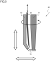
- FIG. 5 is a schematic view of a wedge bonding apparatus used in the method for producing the semiconductor device according to the embodiment.
- FIG. 5 is an enlarged view of a tip portion of a bonding head of the wedge bonding apparatus.
- a bonding head 60 of the wedge bonding apparatus of the embodiment includes a wedge tool 61, a cutter blade 62, and a wire guide 63.
- the bonding head 60 can move up, down, left, and right. Further, the bonding head 60 can rotate in a horizontal plane.
- the wedge tool 61 has a groove (not illustrated) for holding a wire 70 at the distal end.
- the wire 70 and a portion to be connected are bonded by applying ultrasonic vibration in a state in which the wire 70 is pressed against the portion to be connected by the wedge tool 61.
- the cutter blade 62 has a function of cutting the wire 70.
- the cutter blade 62 can move in the vertical direction independently with respect to the wedge tool 61 and the wire guide 63.
- the wire guide 63 has a function of feeding the wire 70 to the wedge tool 61.
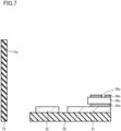
- FIGS. 6 , 7 , 8 , 9 , 10 , 11 , 12 , 13 , 14 , and 15 are schematic views illustrating the method for producing the semiconductor device according to the embodiment.
- FIGS. 6 to 15 are views corresponding to the cross section illustrated in FIG. 4 .
- FIGS. 6 to 15 are views illustrating a method for forming the first bonding wire 41 illustrated in FIG. 4 .
- the resin case 10 is an example of a frame body.
- the first metal layer 31 and the second metal layer 32 are provided on the surface of the insulating substrate 30.
- the second metal layer 32 is located between the first metal layer 31 and the wall surface 10a.
- the first MOSFET 38 is disposed on the first metal layer 31 ( FIG. 7 ).
- the first MOSFET 38 is an example of a semiconductor chip.
- the first MOSFET 38 is bonded to the first metal layer 31.
- the first MOSFET 38 includes the gate electrode pad 38a, the source electrode 38b, the semiconductor layer 38c, and the drain electrode 38d.
- the gate electrode pad 38a is an example of an electrode.
- the first bonding wire 41 is formed using the wedge bonding apparatus.
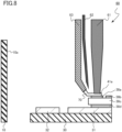
- the wire 70 is pressed against the surface of the gate electrode pad 38a by the wedge tool 61 to form the first bond portion 41a ( FIG. 8 ).
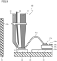
- the bonding head 60 is moved in the lateral direction to form the loop portion 41c ( FIG. 9 ).
- the loop portion 41c is an example of an intermediate portion.
- the bonding head 60 moves in the first direction illustrated in FIG. 3 .
- the loop portion 41c extends in the first direction illustrated in FIG. 3 .
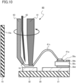
- the bonding head 60 is rotated in a plane horizontal to the surface of the second metal layer 32 ( FIG. 10 ).
- the rotation angle is, for example, 10 degrees or more and 90 degrees or less.
- the rotation angle is preferably, for example, 20 degrees or more and 45 degrees or less.
- the wire 70 is pressed against the surface of the second metal layer 32 by the wedge tool 61 to form the second bond portion 41b ( FIG. 11 ).
- the second bond portion 41b extends in the second direction illustrated in FIG. 3 .
- the wire 70 is half-cut by the cutter blade 62 ( FIG. 12 ).
- the bonding head 60 is moved in the lateral direction while the wire 70 is fed out from the wire guide 63 ( FIG. 14 ).
- the bonding head 60 is moved toward the wall surface 10a.
- the bonding head 60 is moved in the second direction illustrated in FIG. 3 .
- the wire 70 fed from the wire guide 63 serves as the first bond portion when the next wire bonding is formed.
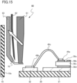
- the bonding head 60 is moved obliquely upward, and the wire 70 is pulled to be completely cut ( FIG. 15 ).
- the bonding head 60 is moved in the direction of the wall surface 10a. At this time, the bonding head 60 is moved in the second direction illustrated in FIG. 3 .
- the first bonding wire 41 is formed by the above method.
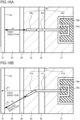
- FIGS. 16A and 16B are explanatory views of functions and effects of the semiconductor device and the method for producing the semiconductor device according to the embodiment.
- FIG. 16A is an enlarged schematic top view of a semiconductor device of comparative example.
- FIG. 16B is an enlarged schematic top view of the semiconductor device according to the embodiment.
- FIGS. 16A and 16B are views corresponding to FIG. 3 .
- a bonding wire 49 of the semiconductor device of the comparative example includes a first bond portion 49a, a second bond portion 49b, and a loop portion 49c.
- the bonding wire 49 of the comparative example is different from the first bonding wire 41 of the embodiment in that the second bond portion 49b extends in the first direction similarly to the loop portion 49c.
- the distance dx in the first direction from the end of the second bond portion 49b to the wall surface 10a is smaller than the distance dy in the second direction from the end of the second bond portion 41b of the first bonding wire 41 to the wall surface 10a of the embodiment.
- FIG. 17 is an explanatory view of a problem of the semiconductor device of the comparative example.
- FIG. 17 is a view illustrating a method for forming the bonding wire 49 of the semiconductor device of the comparative example.
- FIG. 17 is a view corresponding to FIG. 15 of the method for producing the semiconductor device according to the embodiment.
- the second bond portion 41b extends in the second direction different from the first direction.
- the second angle ⁇ 2 formed between the second direction and the wall surface 10a of the resin case 10 is smaller than the first angle ⁇ 1 formed between the first direction and the wall surface 10a of the resin case 10.
- the distance dy in the second direction from the end of the second bond portion 41b to the wall surface 10a when the wire 70 of the embodiment is cut is larger than the distance dx in the first direction from the end of the second bond portion 49b to the wall surface 10a of the comparative example. Therefore, in the embodiment, the collision of the bonding head 60 with the wall surface 10a is prevented.
- the collision of the bonding head 60 with the wall surface 10a is suppressed, so that the distance in the first direction from the second bond portion 41b of the first bonding wire 41 to the wall surface 10a can be made smaller than that of the comparative example. Therefore, miniaturization of the power semiconductor module 100 can be achieved.
- the difference between the first angle ⁇ 1 and the second angle ⁇ 2 is preferably 10 degrees or more, more preferably 20 degrees or more, and still more preferably 30 degrees or more.
- the electrode to which the first bond portion 41a of the first bonding wire 41 is connected is preferably the gate electrode pad 38a of a MOSFET or an IGBT as in the embodiment.
- a large current does not flow through the gate electrode pad 38a as compared with the source electrode 38b and the drain electrode 38d. Therefore, the size of the metal layer to which the second bond portion 41b is connected is reduced. For example, the width of the metal layer in the direction perpendicular to the wall surface 10a decreases. Therefore, the distance from the second bond portion 41b of the first bonding wire 41 to the wall surface 10a is likely to be shortened, and the semiconductor device and the method for producing the semiconductor device of the embodiment function effectively.
- the semiconductor chip is not limited thereto.
- other transistors and diodes such as a Schottky barrier diode (SBD) and a PIN diode can be applied.
- SBD Schottky barrier diode
- PIN diode a PIN diode
- a combination of a transistor and a diode can also be applied.
- the "two-in-one" module has been described as an example, but for example, a "four-in-one” module or a “six-in-one” module may be used.
- the number of semiconductor chips is two has been described as an example, but the number of semiconductor chips may be one or three or more.
Landscapes
- Wire Bonding (AREA)
- Engineering & Computer Science (AREA)
- Chemical & Material Sciences (AREA)
- Ceramic Engineering (AREA)
- Manufacturing & Machinery (AREA)
Abstract
A semiconductor device according to the embodiment includes: a frame body (10) having a wall surface (10a); an insulating substrate (30) surrounded by the frame body (10), the insulating substrate (30) having a first metal layer (31) and a second metal layer (32) on a surface, the second metal layer (32) being located between the first metal layer (31) and the wall surface(10a); a semiconductor chip (38) including an electrode (38a) and provided on the first metal layer (31); and a bonding wire (41) having a first bond portion (41a) connected to the electrode (38a), a second bond portion (41b) connected to the second metal layer (32), and an intermediate portion (41c) between the first bond portion (41a) and the second bond portion (41b); wherein a second angle (Θ2) formed between a second direction in which the second bond portion (41b) extends and the wall surface (10a) is smaller than a first angler (Θ1) formed between a first direction in which the intermediate portion (41c) extends and the wall surface (10a).
Description
- This application is based upon and claims the benefit of priority from
Japanese Patent Application No. 2022-039795, filed on March 15, 2022 - Embodiments described herein relate generally to a semiconductor device and a method for producing the semiconductor device.
- In a power semiconductor module, for example, a power semiconductor chip is mounted on a metal base with an insulating substrate interposed between the power semiconductor chip and the metal base. The power semiconductor chip is, for example, a metal oxide semiconductor field effect transistor (MOSFET), an insulated gate bipolar transistor (IGBT), or a diode.
- In order to realize miniaturization of a device on which the power semiconductor module is to be mounted, miniaturization of the power semiconductor module is desired.
-
-
FIG. 1 is a schematic top view of a semiconductor device according to an embodiment; -
FIG. 2 is a schematic cross-sectional view of the semiconductor device according to the embodiment; -
FIG. 3 is an enlarged schematic top view of the semiconductor device according to the embodiment; -
FIG. 4 is an enlarged schematic cross-sectional view of the semiconductor device according to the embodiment; -
FIG. 5 is a schematic view of a wedge bonding apparatus used in a method for producing the semiconductor device according to the embodiment; -
FIG. 6 is a schematic view illustrating the method for producing the semiconductor device according to the embodiment; -
FIG. 7 is a schematic view illustrating the method for producing the semiconductor device according to the embodiment; -
FIG. 8 is a schematic view illustrating the method for producing the semiconductor device according to the embodiment; -
FIG. 9 is a schematic view illustrating the method for producing the semiconductor device according to the embodiment; -
FIG. 10 is a schematic view illustrating the method for producing the semiconductor device according to the embodiment; -
FIG. 11 is a schematic view illustrating the method for producing the semiconductor device according to the embodiment; -
FIG. 12 is a schematic view illustrating the method for producing the semiconductor device according to the embodiment; -
FIG. 13 is a schematic view illustrating the method for producing the semiconductor device according to the embodiment; -
FIG. 14 is a schematic view illustrating the method for producing the semiconductor device according to the embodiment; -
FIG. 15 is a schematic view illustrating the method for producing the semiconductor device according to the embodiment; -
FIGS. 16A and 16B are explanatory views of functions and effects of the semiconductor device and the method for producing the semiconductor device according to the embodiment; and -
FIG. 17 is an explanatory view of a problem of a semiconductor device of comparative example. - A semiconductor device according to an aspect of the present disclosure includes: a frame body having a wall surface; an insulating substrate surrounded by the frame body, the insulating substrate having a first metal layer and a second metal layer on a surface, the second metal layer being located between the first metal layer and the wall surface; a semiconductor chip including an electrode and provided on the first metal layer; and a bonding wire having a first bond portion connected to the electrode, a second bond portion connected to the second metal layer, and an intermediate portion between the first bond portion and the second bond portion; wherein a second angle formed between a second direction in which the second bond portion extends and the wall surface is smaller than a first angle formed between a first direction in which the intermediate portion extends and the wall surface.
- In the present specification, the same or similar members are denoted by the same reference numerals, and redundant description may be omitted.
- In the present specification, in order to indicate a positional relationship of components and the like, an upward direction in the drawings may be described as "upper", and a downward direction in the drawings may be described as "lower". In the present specification, the concepts of "upper" and "lower" are not necessarily terms indicating the relationship with the direction of gravity.
- A semiconductor device according to the embodiment includes: a frame body having a wall surface; an insulating substrate surrounded by the frame body, the insulating substrate having a first metal layer and a second metal layer on a surface, the second metal layer being located between the first metal layer and the wall surface; a semiconductor chip including an electrode and provided on the first metal layer; and a bonding wire having a first bond portion connected to the electrode, a second bond portion connected to the second metal layer, and an intermediate portion between the first bond portion and the second bond portion. A second angle formed between a second direction in which the second bond portion extends and the wall surface is smaller than a first angle formed between a first direction in which the intermediate portion extends and the wall surface.
-
FIG. 1 is a schematic top view of the semiconductor device according to the embodiment.FIG. 2 is a schematic cross-sectional view of the semiconductor device according to the embodiment.FIG. 2 is a cross section taken along line AA' inFIG. 1 . - The semiconductor device of the embodiment is a
power semiconductor module 100. As illustrated inFIG. 1 , in thepower semiconductor module 100 of the embodiment, two MOSFETs are connected in series. The power semiconductor module of the embodiment is a so-called "two-in-one" module in which a half bridge circuit can be configured by one module. For example, a three-phase inverter circuit can be configured by using three power semiconductor modules of the embodiment. - The
power semiconductor module 100 of the embodiment includes a resin case 10 (frame body), alid 12, a firstmain terminal 14, a secondmain terminal 16, anAC output terminal 18, afirst gate terminal 21, asecond gate terminal 22, ametal base 24, aninsulating substrate 30, afirst metal layer 31, asecond metal layer 32, athird metal layer 33, afourth metal layer 34, afifth metal layer 35, abackside metal layer 36, a first MOSFET 38 (semiconductor chip), asecond MOSFET 40, a first bonding wire 41 (bonding wire), asecond bonding wire 42, athird bonding wire 43, afourth bonding wire 44, afifth bonding wire 45, asixth bonding wire 46, and asealing resin 50. - The
resin case 10 has awall surface 10a. Thefirst MOSFET 38 includes agate electrode pad 38a (electrode), asource electrode 38b, asemiconductor layer 38c, and adrain electrode 38d. Thefirst bonding wire 41 includes afirst bond portion 41a, asecond bond portion 41b, and aloop portion 41c. Theloop portion 41c is an example of an intermediate portion. -
FIG. 1 is a top view of thepower semiconductor module 100 from which thelid 12 and thesealing resin 50 are removed. - The
metal base 24 is made of, for example, copper. For example, when thepower semiconductor module 100 is mounted on a product, a heat sink (not illustrated) is connected to the back surface of themetal base 24. - The
insulating substrate 30 is provided above themetal base 24. Theinsulating substrate 30 is surrounded by theresin case 10. Theinsulating substrate 30 is provided between themetal base 24 and thefirst MOSFET 38 and between themetal base 24 and thesecond MOSFET 40. Theinsulating substrate 30 has a function of electrically separating themetal base 24 from thefirst MOSFET 38 and thesecond MOSFET 40. - The
insulating substrate 30 is made of, for example, ceramic. Theinsulating substrate 30 is made of, for example, aluminum oxide, aluminum nitride, or silicon nitride. - The
first metal layer 31, thesecond metal layer 32, thethird metal layer 33, thefourth metal layer 34, and thefifth metal layer 35 are provided on the surface of theinsulating substrate 30. Thefirst metal layer 31, thesecond metal layer 32, thethird metal layer 33, thefourth metal layer 34, and thefifth metal layer 35 are made of, for example, copper. - The
second metal layer 32 is located between thefirst metal layer 31 and thewall surface 10a of theresin case 10. Thefourth metal layer 34 is located between thethird metal layer 33 and thewall surface 10a of theresin case 10. - The
backside metal layer 36 is provided on the back surface of theinsulating substrate 30. Thebackside metal layer 36 is made of, for example, copper. Thebackside metal layer 36 is bonded to themetal base 24 by using, for example, a solder layer or a metal nanoparticle layer (not illustrated). - The
resin case 10 is provided around themetal base 24 and theinsulating substrate 30. A part of theresin case 10 is provided on themetal base 24. Theresin case 10 is an example of a frame body. Theresin case 10 has a function of protecting thefirst MOSFET 38, thesecond MOSFET 40, and the insulatingsubstrate 30. Theresin case 10 has awall surface 10a. - The
lid 12 is provided on theresin case 10. Thefirst MOSFET 38 and thesecond MOSFET 40 are disposed between thelid 12 and the insulatingsubstrate 30. Thelid 12 has a function of protecting thefirst MOSFET 38, thesecond MOSFET 40, and the insulatingsubstrate 30. - The
first bonding wire 41, thesecond bonding wire 42, thethird bonding wire 43, thefourth bonding wire 44, thefifth bonding wire 45, and thesixth bonding wire 46 electrically connect the members of thepower semiconductor module 100. Materials of thefirst bonding wire 41, thesecond bonding wire 42, thethird bonding wire 43, thefourth bonding wire 44, thefifth bonding wire 45, and thesixth bonding wire 46 are, for example, aluminum, copper, or gold. - The
first MOSFET 38 is provided above the insulatingsubstrate 30. Thefirst MOSFET 38 has thegate electrode pad 38a, thesource electrode 38b, thesemiconductor layer 38c, and thedrain electrode 38d. Thegate electrode pad 38a is an example of an electrode. - The
first MOSFET 38 is formed using, for example, silicon carbide. Thesemiconductor layer 38c is, for example, a silicon carbide layer. - The
first MOSFET 38 is provided on thefirst metal layer 31. Thedrain electrode 38d is fixed on thefirst metal layer 31 by using, for example, a solder layer or a metal nanoparticle layer (not illustrated). Thedrain electrode 38d is bonded to thefirst metal layer 31. Thedrain electrode 38d is electrically connected to thefirst metal layer 31. - The
source electrode 38b is electrically connected to thefifth metal layer 35. Thesource electrode 38b is electrically connected to thefifth metal layer 35 by thethird bonding wire 43. - The
gate electrode pad 38a is electrically connected to thesecond metal layer 32. Thegate electrode pad 38a is electrically connected to thesecond metal layer 32 by thefirst bonding wire 41. - The
second MOSFET 40 is provided above the insulatingsubstrate 30. Thesecond MOSFET 40 is provided on thethird metal layer 33. - The sealing
resin 50 is filled in theresin case 10. The sealingresin 50 is surrounded by theresin case 10. The sealingresin 50 covers thefirst MOSFET 38, thesecond MOSFET 40, and the insulatingsubstrate 30. - The sealing
resin 50 has a function of protecting thefirst MOSFET 38, thesecond MOSFET 40, and the insulatingsubstrate 30. In addition, the sealingresin 50 has a function of insulating thefirst MOSFET 38, thesecond MOSFET 40, and the insulatingsubstrate 30. - The sealing
resin 50 contains a resin. The sealingresin 50 is, for example, a silicone gel. For example, other resins such as an epoxy resin and a polyimide resin can be applied to the sealingresin 50. - The first
main terminal 14 is electrically connected to thefifth metal layer 35. For example, a negative voltage is applied to the first main terminal 14 from the outside. The firstmain terminal 14 is made of, for example, copper. - The second
main terminal 16 is electrically connected to thethird metal layer 33. For example, a positive voltage is applied to the second main terminal 16 from the outside. The secondmain terminal 16 is made of, for example, copper. - The
AC output terminal 18 is electrically connected to thefirst metal layer 31. One end of theAC output terminal 18 is fixed to thefirst metal layer 31, for example. TheAC output terminal 18 outputs an output current of the half bridge circuit. - The
first gate terminal 21 is electrically connected to thegate electrode pad 38a of thefirst MOSFET 38. Thefirst gate terminal 21 has a function of applying a gate voltage signal for controlling thefirst MOSFET 38 to thegate electrode pad 38a. - The
second gate terminal 22 is electrically connected to the gate electrode pad of thesecond MOSFET 40. Thesecond gate terminal 22 has a function of applying a gate voltage signal for controlling thesecond MOSFET 40 to the gate electrode pad. -
FIG. 3 is an enlarged schematic top view of the semiconductor device according to the embodiment.FIG. 3 is an enlarged view of a region X surrounded by a broken line inFIG. 1 .FIG. 3 is a top view of a state in which thelid 12 and the sealingresin 50 are removed. -
FIG. 4 is an enlarged schematic cross-sectional view of the semiconductor device according to the embodiment.FIG. 4 is a cross-sectional view including a region along the bonding wire ofFIG. 3 . - The
first bonding wire 41 has thefirst bond portion 41a, thesecond bond portion 41b, and theloop portion 41c. - The
first bond portion 41a is connected to thegate electrode pad 38a of thefirst MOSFET 38. Thesecond bond portion 41b is connected to thesecond metal layer 32. Theloop portion 41c is located between thefirst bond portion 41a and thesecond bond portion 41b. - When the
first bonding wire 41 is formed, thefirst bond portion 41a is formed before thesecond bond portion 41b. - The
loop portion 41c extends in the first direction. An angle formed between the first direction and thewall surface 10a of theresin case 10 is a first angle (θ)1 inFIG. 3 ). The first angle θ1 is, for example, 60 degrees or more and 90 degrees or less. - The
second bond portion 41b extends in the second direction. The second direction is different from the first direction. An angle formed between the second direction and thewall surface 10a of theresin case 10 is a second angle (θ2 inFIG. 3 ). The second angle is, for example, 0 degrees or more and 80 degrees or less. - The second angle θ2 is smaller than the first angle θ1. The difference between the first angle θ1 and the second angle θ2 is, for example, 10 degrees or more and 90 degrees or less. The difference between the first angle θ1 and the second angle θ2 is preferably, for example, 20 degrees or more and 45 degrees or less.
- Next, an example of the method for producing the semiconductor device according to the embodiment will be described. Hereinafter, in particular, the formation of the bonding wire will be described.
- A method for producing a semiconductor device according to the embodiment includes: preparing an insulating substrate surrounded by a frame body having a wall surface, the insulating substrate having a first metal layer and a second metal layer on a surface, the second metal layer being located between the first metal layer and the wall surface; disposing a semiconductor chip including an electrode on the first metal layer; forming a first bond portion of a bonding wire on the electrode; forming an intermediate portion of the bonding wire, the intermediate portion extending in a first direction; and forming a second bond portion of the bonding wire on the second metal layer, the second bond portion extending in a second direction; wherein a second angle formed between the second direction and the wall surface is smaller than a first angle formed between the first direction and the wall surface.
-
FIG. 5 is a schematic view of a wedge bonding apparatus used in the method for producing the semiconductor device according to the embodiment.FIG. 5 is an enlarged view of a tip portion of a bonding head of the wedge bonding apparatus. - A
bonding head 60 of the wedge bonding apparatus of the embodiment includes awedge tool 61, acutter blade 62, and awire guide 63. - The
bonding head 60 can move up, down, left, and right. Further, thebonding head 60 can rotate in a horizontal plane. - The
wedge tool 61 has a groove (not illustrated) for holding awire 70 at the distal end. Thewire 70 and a portion to be connected are bonded by applying ultrasonic vibration in a state in which thewire 70 is pressed against the portion to be connected by thewedge tool 61. - The
cutter blade 62 has a function of cutting thewire 70. Thecutter blade 62 can move in the vertical direction independently with respect to thewedge tool 61 and thewire guide 63. - The
wire guide 63 has a function of feeding thewire 70 to thewedge tool 61. -
FIGS. 6 ,7 ,8 ,9 ,10 ,11 ,12 ,13 ,14 , and15 are schematic views illustrating the method for producing the semiconductor device according to the embodiment.FIGS. 6 to 15 are views corresponding to the cross section illustrated inFIG. 4 .FIGS. 6 to 15 are views illustrating a method for forming thefirst bonding wire 41 illustrated inFIG. 4 . - First, the insulating
substrate 30 surrounded by theresin case 10 having thewall surface 10a is prepared (FIG. 6 ). Theresin case 10 is an example of a frame body. - The
first metal layer 31 and thesecond metal layer 32 are provided on the surface of the insulatingsubstrate 30. Thesecond metal layer 32 is located between thefirst metal layer 31 and thewall surface 10a. - Next, the
first MOSFET 38 is disposed on the first metal layer 31 (FIG. 7 ). Thefirst MOSFET 38 is an example of a semiconductor chip. - The
first MOSFET 38 is bonded to thefirst metal layer 31. Thefirst MOSFET 38 includes thegate electrode pad 38a, thesource electrode 38b, thesemiconductor layer 38c, and thedrain electrode 38d. Thegate electrode pad 38a is an example of an electrode. - Next, the
first bonding wire 41 is formed using the wedge bonding apparatus. - First, the
wire 70 is pressed against the surface of thegate electrode pad 38a by thewedge tool 61 to form thefirst bond portion 41a (FIG. 8 ). - Next, the
bonding head 60 is moved in the lateral direction to form theloop portion 41c (FIG. 9 ). Theloop portion 41c is an example of an intermediate portion. Thebonding head 60 moves in the first direction illustrated inFIG. 3 . Theloop portion 41c extends in the first direction illustrated inFIG. 3 . - Next, when the
bonding head 60 reaches a predetermined region where thesecond bond portion 41b is to be formed, thebonding head 60 is rotated in a plane horizontal to the surface of the second metal layer 32 (FIG. 10 ). The rotation angle is, for example, 10 degrees or more and 90 degrees or less. The rotation angle is preferably, for example, 20 degrees or more and 45 degrees or less. - Next, the
wire 70 is pressed against the surface of thesecond metal layer 32 by thewedge tool 61 to form thesecond bond portion 41b (FIG. 11 ). As thebonding head 60 rotates, thesecond bond portion 41b extends in the second direction illustrated inFIG. 3 . - Next, the
wire 70 is half-cut by the cutter blade 62 (FIG. 12 ). - Next, the
cutter blade 62 is separated from the wire 70 (FIG. 13 ). - Next, the
bonding head 60 is moved in the lateral direction while thewire 70 is fed out from the wire guide 63 (FIG. 14 ). Thebonding head 60 is moved toward thewall surface 10a. Thebonding head 60 is moved in the second direction illustrated inFIG. 3 . Thewire 70 fed from thewire guide 63 serves as the first bond portion when the next wire bonding is formed. - Next, in a state in which the
wire 70 is clamped by thewire guide 63, thebonding head 60 is moved obliquely upward, and thewire 70 is pulled to be completely cut (FIG. 15 ). When thewire 70 is cut, thebonding head 60 is moved in the direction of thewall surface 10a. At this time, thebonding head 60 is moved in the second direction illustrated inFIG. 3 . - The
first bonding wire 41 is formed by the above method. - Next, functions and effects of the semiconductor device and the method for producing the semiconductor device according to the embodiment will be described.
-
FIGS. 16A and 16B are explanatory views of functions and effects of the semiconductor device and the method for producing the semiconductor device according to the embodiment.FIG. 16A is an enlarged schematic top view of a semiconductor device of comparative example.FIG. 16B is an enlarged schematic top view of the semiconductor device according to the embodiment.FIGS. 16A and 16B are views corresponding toFIG. 3 . - A
bonding wire 49 of the semiconductor device of the comparative example includes afirst bond portion 49a, asecond bond portion 49b, and aloop portion 49c. Thebonding wire 49 of the comparative example is different from thefirst bonding wire 41 of the embodiment in that thesecond bond portion 49b extends in the first direction similarly to theloop portion 49c. - In the
bonding wire 49 of the comparative example, the distance dx in the first direction from the end of thesecond bond portion 49b to thewall surface 10a is smaller than the distance dy in the second direction from the end of thesecond bond portion 41b of thefirst bonding wire 41 to thewall surface 10a of the embodiment. -
FIG. 17 is an explanatory view of a problem of the semiconductor device of the comparative example.FIG. 17 is a view illustrating a method for forming thebonding wire 49 of the semiconductor device of the comparative example. -
FIG. 17 is a view corresponding toFIG. 15 of the method for producing the semiconductor device according to the embodiment. When thewire 70 is cut, thebonding head 60 is moved in the first direction toward thewall surface 10a. At this time, when the distance dx in the first direction from the end of thesecond bond portion 49b to thewall surface 10a is small, thebonding head 60 collides with thewall surface 10a. Therefore, it is difficult to continue the formation of the wire bonding. - In the embodiment, the
second bond portion 41b extends in the second direction different from the first direction. The second angle θ2 formed between the second direction and thewall surface 10a of theresin case 10 is smaller than the first angle θ1 formed between the first direction and thewall surface 10a of theresin case 10. - Therefore, as illustrated in
FIGS. 16A and 16B , the distance dy in the second direction from the end of thesecond bond portion 41b to thewall surface 10a when thewire 70 of the embodiment is cut is larger than the distance dx in the first direction from the end of thesecond bond portion 49b to thewall surface 10a of the comparative example. Therefore, in the embodiment, the collision of thebonding head 60 with thewall surface 10a is prevented. - In the embodiment, the collision of the
bonding head 60 with thewall surface 10a is suppressed, so that the distance in the first direction from thesecond bond portion 41b of thefirst bonding wire 41 to thewall surface 10a can be made smaller than that of the comparative example. Therefore, miniaturization of thepower semiconductor module 100 can be achieved. - From the viewpoint of reducing the distance in the first direction from the
second bond portion 41b to thewall surface 10a to achieve the miniaturization of thepower semiconductor module 100, the difference between the first angle θ1 and the second angle θ2 is preferably 10 degrees or more, more preferably 20 degrees or more, and still more preferably 30 degrees or more. - The electrode to which the
first bond portion 41a of thefirst bonding wire 41 is connected is preferably thegate electrode pad 38a of a MOSFET or an IGBT as in the embodiment. A large current does not flow through thegate electrode pad 38a as compared with thesource electrode 38b and thedrain electrode 38d. Therefore, the size of the metal layer to which thesecond bond portion 41b is connected is reduced. For example, the width of the metal layer in the direction perpendicular to thewall surface 10a decreases. Therefore, the distance from thesecond bond portion 41b of thefirst bonding wire 41 to thewall surface 10a is likely to be shortened, and the semiconductor device and the method for producing the semiconductor device of the embodiment function effectively. - In the embodiment, the case where the MOSFET or the IGBT is used as the semiconductor chip has been described as an example, but the semiconductor chip is not limited thereto. For example, other transistors and diodes such as a Schottky barrier diode (SBD) and a PIN diode can be applied. A combination of a transistor and a diode can also be applied.
- In the embodiment, the "two-in-one" module has been described as an example, but for example, a "four-in-one" module or a "six-in-one" module may be used.
- In the embodiment, the case where the number of semiconductor chips is two has been described as an example, but the number of semiconductor chips may be one or three or more.
- While certain embodiments have been described, these embodiments have been presented by way of example only, and are not intended to limit the scope of the inventions. Indeed, the semiconductor device and the method for producing the semiconductor device described herein may be embodied in a variety of other forms; furthermore, various omissions, substitutions and changes in the form of the devices and methods described herein may be made without departing from the spirit of the inventions. The accompanying claims and their equivalents are intended to cover such forms or modifications as would fall within the scope and spirit of the inventions.
- It is explicitly stated that all features disclosed in the description and/or the claims are intended to be disclosed separately and independently from each other for the purpose of original disclosure as well as for the purpose of restricting the claimed invention independent of the composition of the features in the embodiments and/or the claims. It is explicitly stated that all value ranges or indications of groups of entities disclose every possible intermediate value or intermediate entity for the purpose of original disclosure as well as for the purpose of restricting the claimed invention, in particular as limits of value ranges.
Claims (10)
- A semiconductor device (100) comprising:a frame body (10) having a wall surface (10a);an insulating substrate (30) surrounded by the frame body (10a), the insulating substrate (30) having a first metal layer (31) and a second metal layer (32) on a surface, the second metal layer (32) being located between the first metal layer (31) and the wall surface (10a);a semiconductor chip (38) including an electrode (38a) and provided on the first metal layer (31); anda bonding wire (41) having a first bond portion (41a) connected to the electrode (38a), a second bond portion (41b) connected to the second metal layer (32), and an intermediate portion (41c) between the first bond portion (41a) and the second bond portion (41b);wherein a second angle (θ2) formed between a second direction in which the second bond portion (41b) extends and the wall surface (10a) is smaller than a first angle (θ1) formed between a first direction in which the intermediate portion (41c) extends and the wall surface (10a).
- The semiconductor device (100) according to claim 1, wherein a difference between the first angle (θ1) and the second angle (θ2) is 10 degrees or more and 90 degrees or less.
- The semiconductor device (100) according to claim 1 or 2, wherein the semiconductor chip (38) is a metal oxide semiconductor field effect transistor or an insulated gate bipolar transistor; and the electrode (38a) is a gate electrode pad (38a).
- The semiconductor device (100) according to any one of claims 1 to 3, wherein when the bonding wire (41) is formed, the first bond portion (41a) is formed before the second bond portion (41b).
- A method for producing a semiconductor device (100), the method comprising:preparing an insulating substrate (30) surrounded by a frame body (10) having a wall surface (10a), the insulating substrate (30) having a first metal layer (31) and a second metal layer (32) on a surface, the second metal layer (32) being located between the first metal layer (31) and the wall surface (10a);disposing a semiconductor chip (38) including an electrode (38a) on the first metal layer (31);forming a first bond portion (41a) of a bonding wire (41) on the electrode (38a);forming an intermediate portion (41c) of the bonding wire (41), the intermediate portion (41c) extending in a first direction; andforming a second bond portion (41b) of the bonding wire (41) on the second metal layer (32), the second bond portion (41b) extending in a second direction;wherein a second angle (θ2) formed between the second direction and the wall surface (10a) is smaller than a first angle (θ1) formed between the first direction and the wall surface (10a).
- The method for producing a semiconductor device (100) according to claim 5, whereinthe bonding wire (41) is formed by a wedge bonding apparatus having a bonding head (60),the bonding head (60) is moved in the first direction in the forming the intermediate portion (41c), andthe bonding head (60) is moved in the second direction after the forming the second bond portion (41b).
- The method for producing a semiconductor device (100) according to claim 5 or 6, wherein an angle formed between the first direction and the second direction is 10 degrees or more and 45 degrees or less.
- The method for producing a semiconductor device (100) according to any one of claims 5 to 7, wherein an angle formed between the first direction and the second direction is 20 degrees or more and 45 degrees or less.
- The method for producing a semiconductor device (100) according to any one of claims 6 to 8, wherein the bonding head (60) is rotated in a plane horizontal to a surface of the second metal layer (32) before the forming the second bond portion (41b).
- The method for producing a semiconductor device according to any one of claims 5 to 9, wherein the semiconductor chip (38) is a metal oxide semiconductor field effect transistor or an insulated gate bipolar transistor; and the electrode (38a) is a gate electrode pad (38a) .
Applications Claiming Priority (1)
| Application Number | Priority Date | Filing Date | Title |
|---|---|---|---|
| JP2022039795A JP7717648B2 (en) | 2022-03-15 | 2022-03-15 | Semiconductor device and manufacturing method thereof |
Publications (1)
| Publication Number | Publication Date |
|---|---|
| EP4246571A1 true EP4246571A1 (en) | 2023-09-20 |
Family
ID=82943066
Family Applications (1)
| Application Number | Title | Priority Date | Filing Date |
|---|---|---|---|
| EP22190766.0A Pending EP4246571A1 (en) | 2022-03-15 | 2022-08-17 | Semiconductor device and method for producing said semiconductor device |
Country Status (4)
| Country | Link |
|---|---|
| US (1) | US20230299038A1 (en) |
| EP (1) | EP4246571A1 (en) |
| JP (1) | JP7717648B2 (en) |
| CN (1) | CN116798903A (en) |
Citations (3)
| Publication number | Priority date | Publication date | Assignee | Title |
|---|---|---|---|---|
| EP2677541A1 (en) * | 2012-06-19 | 2013-12-25 | ABB Technology AG | Method for wire bonding a power semiconductor chip and the corresponding device |
| US9917065B1 (en) * | 2016-09-09 | 2018-03-13 | GM Global Technology Operations LLC | Power module assembly with reduced inductance |
| EP3886154A1 (en) * | 2020-03-24 | 2021-09-29 | Kabushiki Kaisha Toshiba | Semiconductor device |
Family Cites Families (11)
| Publication number | Priority date | Publication date | Assignee | Title |
|---|---|---|---|---|
| JP2003218154A (en) | 2002-01-28 | 2003-07-31 | Nec Kyushu Ltd | Semiconductor device and manufacturing apparatus thereof |
| TWI248186B (en) | 2004-01-09 | 2006-01-21 | Unaxis Internat Tranding Ltd | Method for producing a wedge-wedge wire connection |
| JP4597118B2 (en) | 2006-12-29 | 2010-12-15 | 三洋電機株式会社 | Manufacturing method of semiconductor device |
| JP5734236B2 (en) | 2011-05-17 | 2015-06-17 | 株式会社新川 | Wire bonding apparatus and bonding method |
| EP2765600A4 (en) * | 2011-09-30 | 2015-06-10 | Rohm Co Ltd | SEMICONDUCTOR DEVICE |
| JP5707302B2 (en) | 2011-11-02 | 2015-04-30 | 株式会社 日立パワーデバイス | Power semiconductor module |
| TWI517277B (en) | 2014-02-14 | 2016-01-11 | 新川股份有限公司 | Wire bonding device and method of manufacturing semiconductor device |
| JP6416055B2 (en) | 2015-08-24 | 2018-10-31 | 三菱電機株式会社 | Semiconductor device |
| JP7347047B2 (en) | 2019-09-12 | 2023-09-20 | 富士電機株式会社 | semiconductor equipment |
| JP7200899B2 (en) * | 2019-09-30 | 2023-01-10 | 三菱電機株式会社 | Semiconductor device and method for manufacturing semiconductor device |
| CN116057691A (en) | 2021-02-12 | 2023-05-02 | 富士电机株式会社 | semiconductor module |
-
2022
- 2022-03-15 JP JP2022039795A patent/JP7717648B2/en active Active
- 2022-07-11 CN CN202210810754.8A patent/CN116798903A/en active Pending
- 2022-08-17 EP EP22190766.0A patent/EP4246571A1/en active Pending
- 2022-08-18 US US17/890,554 patent/US20230299038A1/en active Pending
Patent Citations (3)
| Publication number | Priority date | Publication date | Assignee | Title |
|---|---|---|---|---|
| EP2677541A1 (en) * | 2012-06-19 | 2013-12-25 | ABB Technology AG | Method for wire bonding a power semiconductor chip and the corresponding device |
| US9917065B1 (en) * | 2016-09-09 | 2018-03-13 | GM Global Technology Operations LLC | Power module assembly with reduced inductance |
| EP3886154A1 (en) * | 2020-03-24 | 2021-09-29 | Kabushiki Kaisha Toshiba | Semiconductor device |
Also Published As
| Publication number | Publication date |
|---|---|
| JP7717648B2 (en) | 2025-08-04 |
| US20230299038A1 (en) | 2023-09-21 |
| CN116798903A (en) | 2023-09-22 |
| JP2023134878A (en) | 2023-09-28 |
Similar Documents
| Publication | Publication Date | Title |
|---|---|---|
| US9165901B2 (en) | Semiconductor device | |
| US7863725B2 (en) | Power device packages and methods of fabricating the same | |
| JP4989437B2 (en) | Manufacturing method of semiconductor device | |
| US10468387B2 (en) | Semiconductor device having plate-shaped metal terminals facing one another | |
| CN109994447B (en) | semiconductor module | |
| US12191245B2 (en) | Semiconductor device having a curved part in the printed circuit board | |
| US12165965B2 (en) | Semiconductor device | |
| US11705438B2 (en) | Semiconductor device | |
| US10957673B2 (en) | Semiconductor device | |
| TW201705313A (en) | Semiconductor device manufacturing method and semiconductor device | |
| JP7334655B2 (en) | semiconductor equipment | |
| US20190006267A1 (en) | Solid top terminal for discrete power devices | |
| EP4246571A1 (en) | Semiconductor device and method for producing said semiconductor device | |
| US11127714B2 (en) | Printed board and semiconductor device | |
| JP5261637B2 (en) | Circuit device manufacturing method | |
| JP2016086003A (en) | Manufacturing method of power semiconductor device | |
| US20240105666A1 (en) | Semiconductor device | |
| US12444666B2 (en) | Semiconductor device with bent terminals | |
| US20240170373A1 (en) | Semiconductor device | |
| US20240105562A1 (en) | Semiconductor device | |
| US10410985B1 (en) | Semiconductor device | |
| WO2025020417A1 (en) | Semiconductor chip package and manufacturing method therefor | |
| CN117280458A (en) | Semiconductor device | |
| JP2021034622A (en) | Semiconductor devices and manufacturing methods for semiconductor devices |
Legal Events
| Date | Code | Title | Description |
|---|---|---|---|
| PUAI | Public reference made under article 153(3) epc to a published international application that has entered the european phase |
Free format text: ORIGINAL CODE: 0009012 |
|
| STAA | Information on the status of an ep patent application or granted ep patent |
Free format text: STATUS: REQUEST FOR EXAMINATION WAS MADE |
|
| 17P | Request for examination filed |
Effective date: 20220817 |
|
| AK | Designated contracting states |
Kind code of ref document: A1 Designated state(s): AL AT BE BG CH CY CZ DE DK EE ES FI FR GB GR HR HU IE IS IT LI LT LU LV MC MK MT NL NO PL PT RO RS SE SI SK SM TR |
|
| STAA | Information on the status of an ep patent application or granted ep patent |
Free format text: STATUS: EXAMINATION IS IN PROGRESS |
|
| 17Q | First examination report despatched |
Effective date: 20240923 |