EP4243579A2 - Fiducials for laminate structures - Google Patents
Fiducials for laminate structures Download PDFInfo
- Publication number
- EP4243579A2 EP4243579A2 EP23185218.7A EP23185218A EP4243579A2 EP 4243579 A2 EP4243579 A2 EP 4243579A2 EP 23185218 A EP23185218 A EP 23185218A EP 4243579 A2 EP4243579 A2 EP 4243579A2
- Authority
- EP
- European Patent Office
- Prior art keywords
- laminate structure
- fiducials
- opening
- metal layer
- fiducial
- Prior art date
- Legal status (The legal status is an assumption and is not a legal conclusion. Google has not performed a legal analysis and makes no representation as to the accuracy of the status listed.)
- Granted
Links
Images





Classifications
-
- H—ELECTRICITY
- H05—ELECTRIC TECHNIQUES NOT OTHERWISE PROVIDED FOR
- H05K—PRINTED CIRCUITS; CASINGS OR CONSTRUCTIONAL DETAILS OF ELECTRIC APPARATUS; MANUFACTURE OF ASSEMBLAGES OF ELECTRICAL COMPONENTS
- H05K1/00—Printed circuits
- H05K1/02—Details
- H05K1/0266—Marks, test patterns or identification means
-
- H—ELECTRICITY
- H05—ELECTRIC TECHNIQUES NOT OTHERWISE PROVIDED FOR
- H05K—PRINTED CIRCUITS; CASINGS OR CONSTRUCTIONAL DETAILS OF ELECTRIC APPARATUS; MANUFACTURE OF ASSEMBLAGES OF ELECTRICAL COMPONENTS
- H05K1/00—Printed circuits
- H05K1/02—Details
- H05K1/0266—Marks, test patterns or identification means
- H05K1/0269—Marks, test patterns or identification means for visual or optical inspection
-
- H—ELECTRICITY
- H05—ELECTRIC TECHNIQUES NOT OTHERWISE PROVIDED FOR
- H05K—PRINTED CIRCUITS; CASINGS OR CONSTRUCTIONAL DETAILS OF ELECTRIC APPARATUS; MANUFACTURE OF ASSEMBLAGES OF ELECTRICAL COMPONENTS
- H05K1/00—Printed circuits
- H05K1/02—Details
- H05K1/0296—Conductive pattern lay-out details not covered by sub groups H05K1/02 - H05K1/0295
- H05K1/0298—Multilayer circuits
-
- H—ELECTRICITY
- H05—ELECTRIC TECHNIQUES NOT OTHERWISE PROVIDED FOR
- H05K—PRINTED CIRCUITS; CASINGS OR CONSTRUCTIONAL DETAILS OF ELECTRIC APPARATUS; MANUFACTURE OF ASSEMBLAGES OF ELECTRICAL COMPONENTS
- H05K1/00—Printed circuits
- H05K1/02—Details
- H05K1/03—Use of materials for the substrate
- H05K1/05—Insulated conductive substrates, e.g. insulated metal substrate
-
- H—ELECTRICITY
- H05—ELECTRIC TECHNIQUES NOT OTHERWISE PROVIDED FOR
- H05K—PRINTED CIRCUITS; CASINGS OR CONSTRUCTIONAL DETAILS OF ELECTRIC APPARATUS; MANUFACTURE OF ASSEMBLAGES OF ELECTRICAL COMPONENTS
- H05K1/00—Printed circuits
- H05K1/02—Details
- H05K1/11—Printed elements for providing electric connections to or between printed circuits
- H05K1/115—Via connections; Lands around holes or via connections
-
- H—ELECTRICITY
- H05—ELECTRIC TECHNIQUES NOT OTHERWISE PROVIDED FOR
- H05K—PRINTED CIRCUITS; CASINGS OR CONSTRUCTIONAL DETAILS OF ELECTRIC APPARATUS; MANUFACTURE OF ASSEMBLAGES OF ELECTRICAL COMPONENTS
- H05K1/00—Printed circuits
- H05K1/18—Printed circuits structurally associated with non-printed electric components
-
- H—ELECTRICITY
- H05—ELECTRIC TECHNIQUES NOT OTHERWISE PROVIDED FOR
- H05K—PRINTED CIRCUITS; CASINGS OR CONSTRUCTIONAL DETAILS OF ELECTRIC APPARATUS; MANUFACTURE OF ASSEMBLAGES OF ELECTRICAL COMPONENTS
- H05K3/00—Apparatus or processes for manufacturing printed circuits
- H05K3/0011—Working of insulating substrates or insulating layers
- H05K3/0017—Etching of the substrate by chemical or physical means
- H05K3/0026—Etching of the substrate by chemical or physical means by laser ablation
-
- H—ELECTRICITY
- H05—ELECTRIC TECHNIQUES NOT OTHERWISE PROVIDED FOR
- H05K—PRINTED CIRCUITS; CASINGS OR CONSTRUCTIONAL DETAILS OF ELECTRIC APPARATUS; MANUFACTURE OF ASSEMBLAGES OF ELECTRICAL COMPONENTS
- H05K3/00—Apparatus or processes for manufacturing printed circuits
- H05K3/0011—Working of insulating substrates or insulating layers
- H05K3/0044—Mechanical working of the substrate, e.g. drilling or punching
- H05K3/0052—Depaneling, i.e. dividing a panel into circuit boards; Working of the edges of circuit boards
-
- H—ELECTRICITY
- H05—ELECTRIC TECHNIQUES NOT OTHERWISE PROVIDED FOR
- H05K—PRINTED CIRCUITS; CASINGS OR CONSTRUCTIONAL DETAILS OF ELECTRIC APPARATUS; MANUFACTURE OF ASSEMBLAGES OF ELECTRICAL COMPONENTS
- H05K3/00—Apparatus or processes for manufacturing printed circuits
- H05K3/02—Apparatus or processes for manufacturing printed circuits in which the conductive material is applied to the surface of the insulating support and is thereafter removed from such areas of the surface which are not intended for current conducting or shielding
- H05K3/04—Apparatus or processes for manufacturing printed circuits in which the conductive material is applied to the surface of the insulating support and is thereafter removed from such areas of the surface which are not intended for current conducting or shielding the conductive material being removed mechanically, e.g. by punching
- H05K3/046—Apparatus or processes for manufacturing printed circuits in which the conductive material is applied to the surface of the insulating support and is thereafter removed from such areas of the surface which are not intended for current conducting or shielding the conductive material being removed mechanically, e.g. by punching by selective transfer or selective detachment of a conductive layer
- H05K3/048—Apparatus or processes for manufacturing printed circuits in which the conductive material is applied to the surface of the insulating support and is thereafter removed from such areas of the surface which are not intended for current conducting or shielding the conductive material being removed mechanically, e.g. by punching by selective transfer or selective detachment of a conductive layer using a lift-off resist pattern or a release layer pattern
-
- H—ELECTRICITY
- H05—ELECTRIC TECHNIQUES NOT OTHERWISE PROVIDED FOR
- H05K—PRINTED CIRCUITS; CASINGS OR CONSTRUCTIONAL DETAILS OF ELECTRIC APPARATUS; MANUFACTURE OF ASSEMBLAGES OF ELECTRICAL COMPONENTS
- H05K2201/00—Indexing scheme relating to printed circuits covered by H05K1/00
- H05K2201/07—Electric details
- H05K2201/0707—Shielding
- H05K2201/0715—Shielding provided by an outer layer of PCB
-
- H—ELECTRICITY
- H05—ELECTRIC TECHNIQUES NOT OTHERWISE PROVIDED FOR
- H05K—PRINTED CIRCUITS; CASINGS OR CONSTRUCTIONAL DETAILS OF ELECTRIC APPARATUS; MANUFACTURE OF ASSEMBLAGES OF ELECTRICAL COMPONENTS
- H05K2201/00—Indexing scheme relating to printed circuits covered by H05K1/00
- H05K2201/09—Shape and layout
- H05K2201/09818—Shape or layout details not covered by a single group of H05K2201/09009 - H05K2201/09809
- H05K2201/09918—Optically detected marks used for aligning tool relative to the PCB, e.g. for mounting of components
-
- H—ELECTRICITY
- H05—ELECTRIC TECHNIQUES NOT OTHERWISE PROVIDED FOR
- H05K—PRINTED CIRCUITS; CASINGS OR CONSTRUCTIONAL DETAILS OF ELECTRIC APPARATUS; MANUFACTURE OF ASSEMBLAGES OF ELECTRICAL COMPONENTS
- H05K2203/00—Indexing scheme relating to apparatus or processes for manufacturing printed circuits covered by H05K3/00
- H05K2203/16—Inspection; Monitoring; Aligning
- H05K2203/166—Alignment or registration; Control of registration
-
- H—ELECTRICITY
- H05—ELECTRIC TECHNIQUES NOT OTHERWISE PROVIDED FOR
- H05K—PRINTED CIRCUITS; CASINGS OR CONSTRUCTIONAL DETAILS OF ELECTRIC APPARATUS; MANUFACTURE OF ASSEMBLAGES OF ELECTRICAL COMPONENTS
- H05K3/00—Apparatus or processes for manufacturing printed circuits
- H05K3/30—Assembling printed circuits with electric components, e.g. with resistors
- H05K3/32—Assembling printed circuits with electric components, e.g. with resistors electrically connecting electric components or wires to printed circuits
- H05K3/34—Assembling printed circuits with electric components, e.g. with resistors electrically connecting electric components or wires to printed circuits by soldering
- H05K3/3452—Solder masks
Definitions
- the present disclosure relates to laminate structures for electronic devices, and particularly to fiducials for laminate structures.
- a typical laminate structure may include a non-conductive body for support and one or more conductive features for connecting the electrical components or electronic modules.
- the conductive features may be any type of conductive structure exposed at a surface of the non-conductive body and may include contact pads, conductive traces, surface-exposed sections of vias, and the like.
- Electrical components such as resistors, capacitors, inductors, resonators, bond wires, and integrated circuits (ICs) are mounted to one or more of the conductive features by a soldering process.
- the conductive features may include one or more contact pads connected to one another by one or more conductive traces.
- one or more circuits can be formed on the laminate structure.
- One or more electrical components that are mounted on the laminate structure can be arranged to form an electronic device or module.
- Laminate structures as disclosed herein may include one or more metal layers and dielectric layers that form a support structure for one or more electronic components or modules that are mounted thereon.
- Fiducials are disclosed that are formed in the laminate structure to provide increased visibility and contrast, thereby improving detection of the fiducials with optical detection equipment of automated machines commonly used in the electronics industry.
- a fiducial is defined by an opening in the laminate structure that extends to a depth within the laminate structure that provides sufficient contrast. Openings for fiducials may be arranged to extend through multiple metal layers and dielectric layers of the laminate structure.
- the openings for the fiducials are formed by a subtractive process, such as laser drilling.
- the fiducial may be coated with additional layers or coatings, such as a metal coating that includes an electromagnetic shield for electronic devices that are mounted on the laminate structure, and the fiducial is configured with sufficient visibility and contrast to be detectable through the additional layers or coatings.
- any of the foregoing aspects, and/or various separate aspects and features as described herein, may be combined for additional advantage. Any of the various features and elements as disclosed herein may be combined with one or more other disclosed features and elements unless indicated to the contrary herein.
- Laminate structures as disclosed herein may include one or more metal layers and dielectric layers that form a support structure for one or more electronic components or modules that are mounted thereon.
- Fiducials are disclosed that are formed in the laminate structure to provide increased visibility and contrast, thereby improving detection of the fiducials with optical detection equipment of automated machines commonly used in the electronics industry.
- a fiducial is defined by an opening in the laminate structure that extends to a depth within the laminate structure that provides sufficient contrast. Openings for fiducials may be arranged to extend through multiple metal layers and dielectric layers of the laminate structure.
- the openings for the fiducials are formed by a subtractive process, such as laser drilling.
- the fiducial may be coated with additional layers or coatings, such as a metal coating that includes an electromagnetic shield for electronic devices that are mounted on the laminate structure, and the fiducial is configured with sufficient visibility and contrast to be detectable through the additional layers or coatings.
- Fiducials have many uses in the electronics industry, including the indication of mounting locations for various electronic components or to indicate the locations of singulation lines for electronic components or electronic modules during fabrication. Fiducials are typically placed in various locations across an electronic substrate and automated equipment is configured with optical detection equipment such as a camera to detect the locations of the fiducials and accordingly perform subsequent fabrication steps. For example, pick-and-place machines may be configured to detect various fiducials with a camera and accordingly place various electronic components at the various fiducial locations. In another example, dicing machines may be configured to detect fiducials with a camera and accordingly scribe, break, saw, or cut electronic devices along dicing lines or streets that are registered with the fiducials.
- FIG. 1A is a top view of a laminate structure 10 on which several fiducials 12-1 to 12-3 have been formed.
- FIG. 1B is a cross-sectional view taken along the section line A-A of FIG. 1A .
- the laminate structure 10 includes a plurality of metal layers 14-1 to 14-6 and a plurality of dielectric layers 16-1 to 16-5.
- the laminate structure 10 may comprise a printed circuit board where the plurality of metal layers 14-1 to 14-6 are laminated in an alternating configuration with the plurality of dielectric layers 16-1 to 16-5. While six metal layers 14-1 to 14-6 are illustrated, the laminate structure may be configured with any number of metal layers.
- the plurality of metal layers 14-1 to 14-6 may include copper (Cu), copper foil, or the like while the plurality of dielectric layers 16-1 to 16-5 may include fiber materials, glass, epoxy, glass-reinforced epoxy, ceramic materials, polymer materials and combinations thereof.
- the fiducials 12-1 to 12-3 may be formed on the laminate structure 10 in locations that are spaced apart from mounting regions for various electronic components.
- the fiducials 12-1 to 12-3 may form any number of shapes including circles, crosses, squares, rectangles, and ovals, among others.
- the fiducial 12-1 is formed with a circular shape in a portion of the first metal layer 14-1 where boundaries of the circular shape are defined by a pattern of the first metal layer 14-1.
- a clearance section that is devoid of the first metal layer 14-1 is formed adjacent to the boundaries of the fiducial 12-1, and accordingly, the first dielectric layer 16-1 is visible in the clearance section.
- the fiducial 12-2 also forms a circular shape where boundaries of the circular shape are defined by a pattern of the first metal layer 14-1; however, the fiducial 12-2 is formed by an area of the laminate structure 10 that is devoid of the first metal layer 14-1.
- the fiducial 12-3 forms a cross or plus symbol that is also defined by a pattern of the first metal layer 14-1.
- Each of the fiducials 12-1 to 12-3 may be formed by selectively removing or selectively depositing the first metal layer 14-1. In this manner, the fiducials 12-1 to 12-3 are formed by patterns of the first metal layer 14-1 and portions of the first dielectric layer 16-1 that are visible through the patterns of the first metal layer 14-1.
- a depth of each of the fiducials 12-1 to 12-3 is defined by a thickness of the first metal layer 14-1.
- the laminate structure 10 may be subsequently coated with one or more additional layers (e.g., dielectrics, metals, etc.) in fabrication steps associated with various electronic components that are mounted to the laminate structure 10. If the fiducials 12-1 to 12-3 are also coated with the one or more additional layers, the visibility and/or contrast of the fiducials 12-1 to 12-3 may be reduced, making it more difficult for automated machines to detect the precise location of the fiducials 12-1 to 12-3.
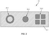
- FIG. 2 is a top view of a laminate structure 18 where several fiducials 20-1 to 20-3 have been formed with increased depths into the laminate structure 18 according to embodiments disclosed herein.
- the first metal layer 14-1 as previously described is visible from the top view.
- the fiducial 20-1 is formed with a circular shape in a portion of the first metal layer 14-1 where an outer boundary of the circular shape is defined by a circular pattern of the first metal layer 14-1. Within the outer boundary, a ring-shaped area is formed that is devoid of the first metal layer 14-1. The ring-shaped area is configured to extend into the laminate structure 18 to a depth sufficient to provide improved visibility and contrast of the fiducial 20-1.
- the fiducial 20-2 also forms a circular shape where an outer boundary of the circular shape is defined by a pattern of the first metal layer 14-1; however, the entire area within the outer boundary of the circular shape is devoid of the first metal layer 14-1 and extends into the laminate structure 18 to a similar depth.
- the fiducial 20-3 forms a cross or plus symbol that is also defined by a pattern of the first metal layer 14-1. In this manner, each of the fiducials 20-1 to 20-3 are formed in the laminate structure 18 and each of the fiducials 20-1 to 20-3 are defined by one or more openings of the first metal layer 14-1.
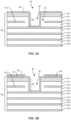
- FIGS. 3A to 3E illustrate cross-sectional views taken at various stages of fabrication for fiducials according to embodiments disclosed herein.
- FIG. 3A is a cross-sectional view of a laminate structure 22 before any fiducials have been formed.
- the laminate structure 22 includes the plurality of metal layers 14-1 to 14-6 and the plurality of dielectric layers 16-1 to 16-5 as previously described.
- the second metal layer 14-2 is formed with an opening 24 such that the second metal layer 14-2 does not extend across the same area of the laminate structure 22 as the other metal layers 14-1, 14-3 to 14-6.
- the first dielectric layer 16-1 and the second dielectric layer 16-2 may be continuous within the opening 24.
- the opening 24 of the second metal layer 14-2 is formed during fabrication of the laminate structure 22 and may include selectively depositing a pattern of the second metal layer 14-2 to form the opening 24 or blanket depositing the second metal layer 14-2 and selectively removing a portion of the second metal layer 14-2 to form the opening 24.
- FIG. 3B is a cross-sectional view of the laminate structure 22 of FIG. 3A after a resist layer 26 has been patterned on the laminate structure 22.
- the resist layer 26 may be patterned by various methods, including lithography and photolithography.
- the resist layer 26 is formed on the laminate structure 22 and is registered with the opening 24 of the second metal layer 14-2.
- FIG. 3C is a cross-sectional view of the laminate structure 22 of FIG. 3B after a thickness of the first metal layer 14-1 has been increased in certain areas.
- additional material of the first metal layer 14-1 may be formed on the laminate structure 22 around the resist layer 26.
- a thin portion of the first metal layer 14-1 is formed that is between the resist layer 26 and the first dielectric layer 16-1.
- the thickness of the first metal layer 14-1 may be increased by depositing additional Cu material by a plating process or other deposition techniques around the resist layer 26. In other embodiments, a material that is different from the first metal layer 14-1 may be deposited around the resist layer 26.
- FIG. 3D is a cross-sectional view of the laminate structure 22 after the resist layer 26 of FIG. 3C has been removed. In particular, the resist layer 26 of FIG. 3C may be stripped off of the laminate structure 22, and the thinner portion of the first metal layer 14-1 that was directly under the resist layer 26 of FIG. 3C may be etched or otherwise removed to form an opening 28 that is defined by a pattern of the first metal layer 14-1.
- a fiducial 30 that is similar to the fiducial 12-2 of FIG. 1A may be formed where boundaries of the fiducial 30 are defined by a pattern of the first metal layer 14-1. Due to the increased thickness of the first metal layer 14-1 in FIG. 3D , the fiducial 30 is formed with a greater depth into the laminate structure 22 than the fiducial 12-2 of FIG. 1A , thereby providing improved contrast when viewed from above the laminate structure 22. As illustrated, the opening 28 is registered with the opening 24 of the second metal layer 14-2.
- FIG. 3E is a cross-sectional view of the laminate structure 22 of FIG. 3D after a depth of the fiducial 30 is increased even further into the laminate structure 22.
- portions of the first and second dielectric layers 16-1, 16-2 that were registered with the opening 28 are removed such that the opening 28 is configured to extend to the third metal layer 14-3.
- the shape of the opening 28 is defined by a pattern of the first metal layer 14-1, the first dielectric layer 16-1, and the second dielectric layer 16-2, and the fiducial 30 comprises a surface of the third metal layer 14-3 that is exposed by the opening 28.
- the opening 28 is thereby configured to extend through the opening 24 of the second metal layer 14-2.
- the fiducial 30 is formed in the laminate structure 22 and the fiducial 30 is defined by the opening 28 that extends through the first metal layer 14-1, the first dielectric layer 16-1, and the second metal layer 14-2.
- a width of the opening 28 may define a width of the fiducial 30.
- a sidewall 28' of the opening 28 comprises a portion of the first metal layer 14-1 and a portion of the first dielectric layer 16-1.
- the sidewall 28' may also comprise a portion of the second dielectric layer 16-2.
- the sidewall 28' may also refer to a sidewall of the laminate structure 22 that is within the opening 28 and the sidewall 28' may also be configured to define at least a portion of the fiducial 30.
- the opening 24 in the second metal layer 14-2 is configured with a larger width across the laminate structure 22 than a width of the opening 28.
- the sidewall 28' may be devoid of the second metal layer 14-2.
- the fiducial 30 is configured to extend further into the laminate structure 22, thereby providing even further improved visibility and contrast when viewed from above the laminate structure 22. Additionally, at least some portions of the fiducial 30 are defined by edges of the first metal layer 14-1 at the opening 28, thereby forming a well-defined edge for optical detection equipment.
- a selective removal process may be performed on the laminate structure 22 in certain embodiments.
- the selective removal process may comprise laser drilling where pulsed laser energy from a laser source such as a carbon dioxide (CO 2 ) laser is applied to the laminate structure 22 at the opening 28.
- the laser energy may be configured to be absorbed by and promote ablation of the first and second dielectric layers 16-1, 16-2. Additionally, the laser energy may be configured to have reduced absorption by the metal layers 14-1, 14-3. In this regard, the laser energy may be applied over a wider area of the laminate structure 22 and the shape of the fiducial 30 will be defined by the pattern or opening 28 that extends through the first metal layer 14-1.
- different depths of fiducials 30 may be configured by initially arranging additional openings of various metal layers within the laminate structure 22.
- the third metal layer 14-3 may be formed with an opening similar to the opening 24 of the second metal layer 14-2.
- a laser drilling process may ablate portions of the first, second, and third dielectric layers 16-1 to 16-3 before stopping at the fourth metal layer 14-4.
- Other subtractive removal steps are contemplated, including mechanical drilling or cutting, and etching, among others.
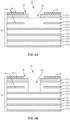
- FIG. 4A is a cross-sectional view of a laminate structure 32 that includes a solder mask 34 according to embodiments disclosed herein.
- the laminate structure 32 is similar to the laminate structure 22 of FIG. 3D and accordingly includes the metal layers 14-1 - 14-6, the dielectric layers 16-1 - 16-5, the opening 28 that is defined by a pattern of the first metal layer 14-1, and the fiducial 30 as previously described.
- the solder mask 34 may be configured to provide electrical isolation on the top of the laminate structure 32 as well as to provide oxidation protection.
- the solder mask 34 may be configured on the first metal layer 14-1 to form a solder mask opening 36 that is registered with the fiducial 30.
- the solder mask opening 36 is configured with a larger width across the laminate structure 32 than a width of the fiducial 30 across the laminate structure 32. Accordingly, a portion of the first metal layer 14-1 that is closest to the opening 28 may be devoid of the solder mask 34 to provide access to the opening 28 in subsequent processing steps as well as to provide increased visibility of the fiducial 30.
- FIG. 4B is a cross-sectional view of the laminate structure 32 of FIG. 4A after a depth of the fiducial 30 is increased.
- the depth of the fiducial 30 may be increased by a subtractive material process, such as the laser drilling as previously described for FIG. 3E .
- a subtractive material process such as the laser drilling as previously described for FIG. 3E .
- one or more additional layers or coatings may be applied to surfaces of laminate structures as disclosed herein.
- one or more additional layers may include additional dielectric coatings and/or additional metal coatings, among others.
- electrical components or modules on a laminate structure may be coated with one or more metal coatings to form an electromagnetic shield for reducing electromagnetic interference or crosstalk between different ones of the electrical components or modules.
- An electromagnetic shield may include one or more thin metal layers sequentially deposited over a laminate structure to cover a particular electrical component or module.
- An electromagnetic shield may also include one or more metal particles or flecks suspended in a binder.
- fiducials that are provided in the laminate structure may also be coated with the electromagnetic shield coatings. According to configurations of fiducials as disclosed herein, fiducials may be coated with additional layers or coatings and still maintain sufficient visibility and contrast to be viewed and detected with automated processing equipment.
- FIG. 5A is cross-sectional view of a laminate structure 38 that includes a metal coating 40 on the laminate structure 38 according to embodiments disclosed herein.
- the metal coating 40 may comprise one or more layers or sub-layers that form an electromagnetic shield for electrical components or modules that are mounted in other locations of the laminate structure 38.
- the metal coating 40 may be deposited by one or more combinations of electroless plating, electrolytic plating, other plating processes, sputtering, dispensing, and spraying, among others.
- the metal coating 40 comprises one or more layers of Cu, nickel (Ni), and combinations thereof.
- the metal coating 40 may comprise a first layer of electroless Cu, a second layer of electrolytic Cu, and a third layer of electrolytic Ni to form an electromagnetic shield.
- the metal coating 40 comprises conductive metal particles or flecks that are suspended or filled in an epoxy material or binder to form an electromagnetic shield.
- the epoxy material may be filed with one or more combinations of conductive metal particles or flecks of Cu, silver (Ag), tin/zinc alloys (Sn/Zn), or other conductive materials.
- the laminate structure 38 in FIG. 5A is similar to the laminate structure 22 of FIG. 3E and accordingly includes the metal layers 14-1 to 14-6, the dielectric layers 16-1 to 16-5, the opening 28 that is defined by a pattern of the first metal layer 14-1, and the fiducial 30 as previously described. During deposition of the metal coating 40, the opening 28 may also be covered by the metal coating 40.
- the metal coating 40 may be configured to extend into the opening 28 and to cover the sidewall 28'. In certain embodiments, the metal coating 40 may be configured to extend into the opening 28 to cover the surface of the third metal layer 14-3 that is exposed by the opening 28. As illustrated, the fiducial 30 is defined by the opening 28 and the metal coating 40 is configured to cover one or more surfaces of the laminate structure 38 that are outside of the opening 28 (e.g., top surfaces of the first metal layer 14-1) as well as one or more surfaces of the laminate structure 38 that are within the opening 28 (e.g., the sidewall 28' and a portion of the third metal layer 14-3).
- FIG. 5B is a cross-sectional view of the laminate structure 38 of FIG. 5A for embodiments that include the solder mask 34 as described for FIG. 4A and FIG. 4B .
- the solder mask 34 may be configured as previously described and the metal coating 40 may subsequently be formed on the laminate structure 38 to cover at least a portion of the solder mask 34.
- the metal coating 40 may also be configured to cover portions of the first metal layer 14-1 that are uncovered by the solder mask 34, and the metal coating 40 may also be configured to extend into the opening 28 as previously described.
- the metal coating 40 covers the sidewall 28' of the opening 28 as well as a portion of the third metal layer 14-3 within the opening 28.
- a laminate structure as disclosed herein may be populated with arrays of one or more electronic components that form an array of electronic modules.
- the electronic components are mounted on and electrically connected to one or more of the metal layers of the laminate structure.
- the laminate structure may be diced or singulated along dicing lines or streets that extend between individual ones or groups of electronic modules, thereby forming a plurality of separated electronic modules.
- Fiducials as described herein may be provided at various locations in the laminate structure. In certain embodiments, fiducials are placed to identify the location of the dicing lines for dicing equipment. In certain embodiments, fiducials may also be placed to identify the locations where individual electronic components are to be mounted for placement equipment.
- FIG. 6A is a top view of a representative laminate structure 42 on which a plurality of electronic modules 44 have been mounted to form an array of the electronic modules 44.
- various combinations of one or more electrical components including resistors, capacitors, inductors, resonators, bond wires, and ICs may form each of the electronic modules 44.
- Streets or dicing lines 46 are configured between rows and columns of the electronic modules 44. For simplicity, only a few dicing lines 46 are shown, but it is understood dicing lines 46 can be formed between every column and every row of the electronic modules 44.
- a plurality of fiducials 30 are arranged in the laminate structure 42 as previously described. As illustrated in FIG.
- the plurality of fiducials 30 are configured in areas of the laminate structure 42 that are spaced apart from where the electronic modules 44 are mounted.
- the fiducials 30 are arranged along the perimeter of the laminate structure 42 and the fiducials 30 are configured to be registered with or aligned with the dicing lines 46.
- an automated dicing machine may be configured to detect the location of each fiducial 30 and properly align the machine to cut, saw, break, or otherwise separate the laminate structure 42 along each of the dicing lines 46.
- each of the fiducials 30 may comprise an alignment marker that indicates the location of each dicing line 46 for singulation.
- the dicing lines 46 or streets may comprise a width as measured by a distance between adjacent electronic modules 44 in a range of about 100 microns ( ⁇ m) to about 500 ⁇ m.
- the fiducials 30 are registered with the width of the dicing lines 46.
- the fiducials 30 may comprise a longest dimension across the surface (e.g., diameter for circular fiducials) of the laminate structure 42 that is approximately the same as the width of the dicing lines 46.
- the fiducials 30 may comprise a longest dimension across the surface of the laminate structure 42 that is less than the width of the dicing lines 46.
- the fiducials 30 may comprise a longest dimension across the surface of the laminate structure 42 that is greater than the width of the dicing lines 46.
- the fiducials 30 may be registered with the dicing lines 46 such that a center point of each fiducial 30 is aligned with at least one dicing line 46.
- the longest dimension of the fiducials 30 across the surface of the laminate structure 42 may include a range from about 100 ⁇ m to about 500 ⁇ m, or in a range from about 200 ⁇ m to about 400 ⁇ m, or in a range from about 250 ⁇ m to about 350 ⁇ m.
- the fiducials 30 may be provided in locations that are adjacent to each of the electronic modules 44 to indicate a mounting location for each of the electronic modules 44.
- FIG. 6B is a top view of the laminate structure 42 of FIG. 6A after the metal coating 40 as described for FIG. 5A and FIG. 5B has been formed.
- the metal coating 40 is blanket deposited across the plurality of electronic modules 44 and surfaces of the laminate structure 42 that are uncovered by the plurality of electronic modules 44.
- the metal coating 40 may comprise an electromagnetic shield as previously described. In this manner, each of the electronic modules 44 is coated with an electromagnetic shield that will remain on each of the electronic modules 44 after singulation along each of the dicing lines 46.
- the metal coating 40 may also be configured to coat the fiducials 30.
- the fiducials 30 as disclosed herein are provided with increased visibility and contrast at least partly due to the increased depth in which the fiducials 30 are formed within the laminate structure 42. In this manner, the metal coating 40 may not obscure the fiducials 30, thereby allowing the fiducials 30 to remain visible from the top view with sufficient contrast to be detected by cameras or other detection equipment of automated dicing equipment.
Landscapes
- Engineering & Computer Science (AREA)
- Microelectronics & Electronic Packaging (AREA)
- Manufacturing & Machinery (AREA)
- Physics & Mathematics (AREA)
- Optics & Photonics (AREA)
- Production Of Multi-Layered Print Wiring Board (AREA)
- Shielding Devices Or Components To Electric Or Magnetic Fields (AREA)
- Structure Of Printed Boards (AREA)
- Laminated Bodies (AREA)
Abstract
Description
- The present disclosure relates to laminate structures for electronic devices, and particularly to fiducials for laminate structures.
- Electronic substrates are often used to support and connect electrical components and electronic modules. Laminate structures, such as printed circuit boards and the like, are commonly used as electronic substrates for electronic devices. A typical laminate structure may include a non-conductive body for support and one or more conductive features for connecting the electrical components or electronic modules. The conductive features may be any type of conductive structure exposed at a surface of the non-conductive body and may include contact pads, conductive traces, surface-exposed sections of vias, and the like. Electrical components such as resistors, capacitors, inductors, resonators, bond wires, and integrated circuits (ICs) are mounted to one or more of the conductive features by a soldering process. For example, the conductive features may include one or more contact pads connected to one another by one or more conductive traces. Accordingly, one or more circuits can be formed on the laminate structure. One or more electrical components that are mounted on the laminate structure can be arranged to form an electronic device or module.
- In typical fabrication processes, many electronic modules can be formed concurrently across a common laminate structure before individual electronic modules or groups of electronic modules are singulated. In this manner, common manufacturing steps and processes may be sequentially performed at high speeds to concurrently form large quantities of electronic modules. Electronic component placement tools may be utilized to place and mount electronic components across common laminate structures to form the electronic modules. After the electronic modules are formed, singulation may include separating the laminate structure along peripheral boundaries of individual electronic modules or around groups of electronic modules. Fiducials, or recognition marks, are typically employed to indicate the mounting locations of various electronic components on the laminate structure or to indicate the locations of singulation lines for the electronic modules.
- The art continues to seek improved electronic devices and related fabrication techniques capable of overcoming challenges associated with conventional electronic devices.
- The present disclosure relates to laminate structures for electronic devices and more particularly to configurations of fiducials for laminate structures. Laminate structures as disclosed herein may include one or more metal layers and dielectric layers that form a support structure for one or more electronic components or modules that are mounted thereon. Fiducials are disclosed that are formed in the laminate structure to provide increased visibility and contrast, thereby improving detection of the fiducials with optical detection equipment of automated machines commonly used in the electronics industry. In certain embodiments, a fiducial is defined by an opening in the laminate structure that extends to a depth within the laminate structure that provides sufficient contrast. Openings for fiducials may be arranged to extend through multiple metal layers and dielectric layers of the laminate structure. In certain embodiments, the openings for the fiducials are formed by a subtractive process, such as laser drilling. In certain embodiments, the fiducial may be coated with additional layers or coatings, such as a metal coating that includes an electromagnetic shield for electronic devices that are mounted on the laminate structure, and the fiducial is configured with sufficient visibility and contrast to be detectable through the additional layers or coatings.
- In another aspect, any of the foregoing aspects, and/or various separate aspects and features as described herein, may be combined for additional advantage. Any of the various features and elements as disclosed herein may be combined with one or more other disclosed features and elements unless indicated to the contrary herein.
- Those skilled in the art will appreciate the scope of the present disclosure and realize additional aspects thereof after reading the following detailed description of the preferred embodiments in association with the accompanying drawing figures.
- The accompanying drawing figures incorporated in and forming a part of this specification illustrate several aspects of the disclosure, and together with the description serve to explain the principles of the disclosure.
-
FIG. 1A is a top view of a laminate structure on which several fiducials have been formed. -
FIG. 1B is a cross-sectional view taken along the section line A-A ofFIG. 1A -
FIG. 2 is a top view of a laminate structure where several fiducials have been formed with increased depths into the laminate structure according to embodiments disclosed herein. -
FIG. 3A is a cross-sectional view of a laminate structure before any fiducials have been formed. -
FIG. 3B is a cross-sectional view of the laminate structure ofFIG. 3A after a resist layer has been patterned on the laminate structure. -
FIG. 3C is a cross-sectional view of the laminate structure ofFIG. 3B after a thickness of a first metal layer has been increased in certain areas. -
FIG. 3D is a cross-sectional view of the laminate structure ofFIG. 3C after the resist layer has been removed. -
FIG. 3E is a cross-sectional view of the laminate structure ofFIG. 3D after a depth of a fiducial is increased into the laminate structure. -
FIG. 4A is a cross-sectional view of a laminate structure that includes a solder mask according to embodiments disclosed herein. -
FIG. 4B is a cross-sectional view of the laminate structure ofFIG. 4A after a depth of a fiducial is increased. -
FIG. 5A is cross-sectional view of a laminate structure that includes a metal coating on the laminate structure according to embodiments disclosed herein. -
FIG. 5B is a cross-sectional view of the laminate structure ofFIG. 5A for embodiments that include a solder mask as illustrated inFIG. 4A and FIG. 4B . -
FIG. 6A is a top view of a representative laminate structure on which a plurality of electronic modules have been mounted to form an array of the electronic modules. -
FIG. 6B is a top view of the laminate structure ofFIG. 6A after a metal coating as illustrated inFIG. 5A and FIG. 5B has been formed. - The embodiments set forth below represent the necessary information to enable those skilled in the art to practice the embodiments and illustrate the best mode of practicing the embodiments. Upon reading the following description in light of the accompanying drawing figures, those skilled in the art will understand the concepts of the disclosure and will recognize applications of these concepts not particularly addressed herein. It should be understood that these concepts and applications fall within the scope of the disclosure and the accompanying claims.
- It will be understood that, although the terms first, second, etc. may be used herein to describe various elements, these elements should not be limited by these terms. These terms are only used to distinguish one element from another. For example, a first element could be termed a second element, and, similarly, a second element could be termed a first element, without departing from the scope of the present disclosure. As used herein, the term "and/or" includes any and all combinations of one or more of the associated listed items.
- It will be understood that when an element such as a layer, region, or substrate is referred to as being "on" or extending "onto" another element, it can be directly on or extend directly onto the other element or intervening elements may also be present. In contrast, when an element is referred to as being "directly on" or extending "directly onto" another element, there are no intervening elements present. Likewise, it will be understood that when an element such as a layer, region, or substrate is referred to as being "over" or extending "over" another element, it can be directly over or extend directly over the other element or intervening elements may also be present. In contrast, when an element is referred to as being "directly over" or extending "directly over" another element, there are no intervening elements present. It will also be understood that when an element is referred to as being "connected" or "coupled" to another element, it can be directly connected or coupled to the other element or intervening elements may be present. In contrast, when an element is referred to as being "directly connected" or "directly coupled" to another element, there are no intervening elements present.
- Relative terms such as "below" or "above" or "upper" or "lower" or "horizontal" or "vertical" may be used herein to describe a relationship of one element, layer, or region to another element, layer, or region as illustrated in the Figures. It will be understood that these terms and those discussed above are intended to encompass different orientations of the device in addition to the orientation depicted in the Figures.
- The terminology used herein is for the purpose of describing particular embodiments only and is not intended to be limiting of the disclosure. As used herein, the singular forms "a," "an," and "the" are intended to include the plural forms as well, unless the context clearly indicates otherwise. It will be further understood that the terms "comprises," "comprising," "includes," and/or "including" when used herein specify the presence of stated features, integers, steps, operations, elements, and/or components, but do not preclude the presence or addition of one or more other features, integers, steps, operations, elements, components, and/or groups thereof.
- Unless otherwise defined, all terms (including technical and scientific terms) used herein have the same meaning as commonly understood by one of ordinary skill in the art to which this disclosure belongs. It will be further understood that terms used herein should be interpreted as having a meaning that is consistent with their meaning in the context of this specification and the relevant art and will not be interpreted in an idealized or overly formal sense unless expressly so defined herein.
- The present disclosure relates to laminate structures for electronic devices and more particularly to configurations of fiducials for laminate structures. Laminate structures as disclosed herein may include one or more metal layers and dielectric layers that form a support structure for one or more electronic components or modules that are mounted thereon. Fiducials are disclosed that are formed in the laminate structure to provide increased visibility and contrast, thereby improving detection of the fiducials with optical detection equipment of automated machines commonly used in the electronics industry. In certain embodiments, a fiducial is defined by an opening in the laminate structure that extends to a depth within the laminate structure that provides sufficient contrast. Openings for fiducials may be arranged to extend through multiple metal layers and dielectric layers of the laminate structure. In certain embodiments, the openings for the fiducials are formed by a subtractive process, such as laser drilling. In certain embodiments, the fiducial may be coated with additional layers or coatings, such as a metal coating that includes an electromagnetic shield for electronic devices that are mounted on the laminate structure, and the fiducial is configured with sufficient visibility and contrast to be detectable through the additional layers or coatings.
- Fiducials, or recognition marks, have many uses in the electronics industry, including the indication of mounting locations for various electronic components or to indicate the locations of singulation lines for electronic components or electronic modules during fabrication. Fiducials are typically placed in various locations across an electronic substrate and automated equipment is configured with optical detection equipment such as a camera to detect the locations of the fiducials and accordingly perform subsequent fabrication steps. For example, pick-and-place machines may be configured to detect various fiducials with a camera and accordingly place various electronic components at the various fiducial locations. In another example, dicing machines may be configured to detect fiducials with a camera and accordingly scribe, break, saw, or cut electronic devices along dicing lines or streets that are registered with the fiducials.
-
FIG. 1A is a top view of alaminate structure 10 on which several fiducials 12-1 to 12-3 have been formed.FIG. 1B is a cross-sectional view taken along the section line A-A ofFIG. 1A . Thelaminate structure 10 includes a plurality of metal layers 14-1 to 14-6 and a plurality of dielectric layers 16-1 to 16-5. Thelaminate structure 10 may comprise a printed circuit board where the plurality of metal layers 14-1 to 14-6 are laminated in an alternating configuration with the plurality of dielectric layers 16-1 to 16-5. While six metal layers 14-1 to 14-6 are illustrated, the laminate structure may be configured with any number of metal layers. Generally, increasing the number of laminated metal layers corresponds to an increased number of electronic components that may be mounted and electrically connected on a particular laminate structure. This allows electrical connections to various electronic components to be made at different horizontal planes within thelaminate structure 10. In certain embodiments, the plurality of metal layers 14-1 to 14-6 may include copper (Cu), copper foil, or the like while the plurality of dielectric layers 16-1 to 16-5 may include fiber materials, glass, epoxy, glass-reinforced epoxy, ceramic materials, polymer materials and combinations thereof. The fiducials 12-1 to 12-3 may be formed on thelaminate structure 10 in locations that are spaced apart from mounting regions for various electronic components. Depending on the detection equipment utilized, the fiducials 12-1 to 12-3 may form any number of shapes including circles, crosses, squares, rectangles, and ovals, among others. As illustrated inFIG. 1A , the fiducial 12-1 is formed with a circular shape in a portion of the first metal layer 14-1 where boundaries of the circular shape are defined by a pattern of the first metal layer 14-1. A clearance section that is devoid of the first metal layer 14-1 is formed adjacent to the boundaries of the fiducial 12-1, and accordingly, the first dielectric layer 16-1 is visible in the clearance section. In another example, the fiducial 12-2 also forms a circular shape where boundaries of the circular shape are defined by a pattern of the first metal layer 14-1; however, the fiducial 12-2 is formed by an area of thelaminate structure 10 that is devoid of the first metal layer 14-1. In yet another example, the fiducial 12-3 forms a cross or plus symbol that is also defined by a pattern of the first metal layer 14-1. Each of the fiducials 12-1 to 12-3 may be formed by selectively removing or selectively depositing the first metal layer 14-1. In this manner, the fiducials 12-1 to 12-3 are formed by patterns of the first metal layer 14-1 and portions of the first dielectric layer 16-1 that are visible through the patterns of the first metal layer 14-1. Accordingly, a depth of each of the fiducials 12-1 to 12-3 is defined by a thickness of the first metal layer 14-1. Depending on the application, thelaminate structure 10 may be subsequently coated with one or more additional layers (e.g., dielectrics, metals, etc.) in fabrication steps associated with various electronic components that are mounted to thelaminate structure 10. If the fiducials 12-1 to 12-3 are also coated with the one or more additional layers, the visibility and/or contrast of the fiducials 12-1 to 12-3 may be reduced, making it more difficult for automated machines to detect the precise location of the fiducials 12-1 to 12-3. -
FIG. 2 is a top view of alaminate structure 18 where several fiducials 20-1 to 20-3 have been formed with increased depths into thelaminate structure 18 according to embodiments disclosed herein. The first metal layer 14-1 as previously described is visible from the top view. The fiducial 20-1 is formed with a circular shape in a portion of the first metal layer 14-1 where an outer boundary of the circular shape is defined by a circular pattern of the first metal layer 14-1. Within the outer boundary, a ring-shaped area is formed that is devoid of the first metal layer 14-1. The ring-shaped area is configured to extend into thelaminate structure 18 to a depth sufficient to provide improved visibility and contrast of the fiducial 20-1. The fiducial 20-2 also forms a circular shape where an outer boundary of the circular shape is defined by a pattern of the first metal layer 14-1; however, the entire area within the outer boundary of the circular shape is devoid of the first metal layer 14-1 and extends into thelaminate structure 18 to a similar depth. The fiducial 20-3 forms a cross or plus symbol that is also defined by a pattern of the first metal layer 14-1. In this manner, each of the fiducials 20-1 to 20-3 are formed in thelaminate structure 18 and each of the fiducials 20-1 to 20-3 are defined by one or more openings of the first metal layer 14-1. -
FIGS. 3A to 3E illustrate cross-sectional views taken at various stages of fabrication for fiducials according to embodiments disclosed herein.FIG. 3A is a cross-sectional view of alaminate structure 22 before any fiducials have been formed. Thelaminate structure 22 includes the plurality of metal layers 14-1 to 14-6 and the plurality of dielectric layers 16-1 to 16-5 as previously described. As illustrated, the second metal layer 14-2 is formed with anopening 24 such that the second metal layer 14-2 does not extend across the same area of thelaminate structure 22 as the other metal layers 14-1, 14-3 to 14-6. In this regard, the first dielectric layer 16-1 and the second dielectric layer 16-2 may be continuous within theopening 24. Theopening 24 of the second metal layer 14-2 is formed during fabrication of thelaminate structure 22 and may include selectively depositing a pattern of the second metal layer 14-2 to form theopening 24 or blanket depositing the second metal layer 14-2 and selectively removing a portion of the second metal layer 14-2 to form theopening 24. -
FIG. 3B is a cross-sectional view of thelaminate structure 22 ofFIG. 3A after a resistlayer 26 has been patterned on thelaminate structure 22. The resistlayer 26 may be patterned by various methods, including lithography and photolithography. InFIG. 3B , the resistlayer 26 is formed on thelaminate structure 22 and is registered with theopening 24 of the second metal layer 14-2.FIG. 3C is a cross-sectional view of thelaminate structure 22 ofFIG. 3B after a thickness of the first metal layer 14-1 has been increased in certain areas. As illustrated, additional material of the first metal layer 14-1 may be formed on thelaminate structure 22 around the resistlayer 26. In this regard, a thin portion of the first metal layer 14-1 is formed that is between the resistlayer 26 and the first dielectric layer 16-1. In certain examples where the first metal layer 14-1 comprises Cu, the thickness of the first metal layer 14-1 may be increased by depositing additional Cu material by a plating process or other deposition techniques around the resistlayer 26. In other embodiments, a material that is different from the first metal layer 14-1 may be deposited around the resistlayer 26.FIG. 3D is a cross-sectional view of thelaminate structure 22 after the resistlayer 26 ofFIG. 3C has been removed. In particular, the resistlayer 26 ofFIG. 3C may be stripped off of thelaminate structure 22, and the thinner portion of the first metal layer 14-1 that was directly under the resistlayer 26 ofFIG. 3C may be etched or otherwise removed to form anopening 28 that is defined by a pattern of the first metal layer 14-1. In this manner, a fiducial 30 that is similar to the fiducial 12-2 ofFIG. 1A may be formed where boundaries of the fiducial 30 are defined by a pattern of the first metal layer 14-1. Due to the increased thickness of the first metal layer 14-1 inFIG. 3D , the fiducial 30 is formed with a greater depth into thelaminate structure 22 than the fiducial 12-2 ofFIG. 1A , thereby providing improved contrast when viewed from above thelaminate structure 22. As illustrated, theopening 28 is registered with theopening 24 of the second metal layer 14-2. -
FIG. 3E is a cross-sectional view of thelaminate structure 22 ofFIG. 3D after a depth of the fiducial 30 is increased even further into thelaminate structure 22. As illustrated, portions of the first and second dielectric layers 16-1, 16-2 that were registered with theopening 28 are removed such that theopening 28 is configured to extend to the third metal layer 14-3. In this regard, the shape of theopening 28 is defined by a pattern of the first metal layer 14-1, the first dielectric layer 16-1, and the second dielectric layer 16-2, and the fiducial 30 comprises a surface of the third metal layer 14-3 that is exposed by theopening 28. Notably, theopening 28 is thereby configured to extend through theopening 24 of the second metal layer 14-2. Accordingly, the fiducial 30 is formed in thelaminate structure 22 and the fiducial 30 is defined by theopening 28 that extends through the first metal layer 14-1, the first dielectric layer 16-1, and the second metal layer 14-2. In particular a width of theopening 28 may define a width of the fiducial 30. In certain embodiments, a sidewall 28' of theopening 28 comprises a portion of the first metal layer 14-1 and a portion of the first dielectric layer 16-1. The sidewall 28' may also comprise a portion of the second dielectric layer 16-2. In this manner, the sidewall 28' may also refer to a sidewall of thelaminate structure 22 that is within theopening 28 and the sidewall 28' may also be configured to define at least a portion of the fiducial 30. In certain embodiments, theopening 24 in the second metal layer 14-2 is configured with a larger width across thelaminate structure 22 than a width of theopening 28. In this regard, the sidewall 28' may be devoid of the second metal layer 14-2. Accordingly, the fiducial 30 is configured to extend further into thelaminate structure 22, thereby providing even further improved visibility and contrast when viewed from above thelaminate structure 22. Additionally, at least some portions of the fiducial 30 are defined by edges of the first metal layer 14-1 at theopening 28, thereby forming a well-defined edge for optical detection equipment. - In order to remove portions of the first and second dielectric layers 16-1, 16-2 that were registered with the
opening 28, a selective removal process may be performed on thelaminate structure 22 in certain embodiments. The selective removal process may comprise laser drilling where pulsed laser energy from a laser source such as a carbon dioxide (CO2) laser is applied to thelaminate structure 22 at theopening 28. The laser energy may be configured to be absorbed by and promote ablation of the first and second dielectric layers 16-1, 16-2. Additionally, the laser energy may be configured to have reduced absorption by the metal layers 14-1, 14-3. In this regard, the laser energy may be applied over a wider area of thelaminate structure 22 and the shape of the fiducial 30 will be defined by the pattern or opening 28 that extends through the first metal layer 14-1. Ablation of the first and second dielectric layers 16-1, 16-2 will occur and may thereby end at the exposed surface of the third metal layer 14-3. In this manner, different depths offiducials 30 may be configured by initially arranging additional openings of various metal layers within thelaminate structure 22. For example, during fabrication of thelaminate structure 22, the third metal layer 14-3 may be formed with an opening similar to theopening 24 of the second metal layer 14-2. Accordingly, a laser drilling process may ablate portions of the first, second, and third dielectric layers 16-1 to 16-3 before stopping at the fourth metal layer 14-4. Other subtractive removal steps are contemplated, including mechanical drilling or cutting, and etching, among others. -
FIG. 4A is a cross-sectional view of alaminate structure 32 that includes asolder mask 34 according to embodiments disclosed herein. Thelaminate structure 32 is similar to thelaminate structure 22 ofFIG. 3D and accordingly includes the metal layers 14-1 - 14-6, the dielectric layers 16-1 - 16-5, theopening 28 that is defined by a pattern of the first metal layer 14-1, and the fiducial 30 as previously described. Depending on the application and the type of components intended to be mounted on other locations of thelaminate structure 32, thesolder mask 34 may be configured to provide electrical isolation on the top of thelaminate structure 32 as well as to provide oxidation protection. Notably, thesolder mask 34 may be configured on the first metal layer 14-1 to form asolder mask opening 36 that is registered with the fiducial 30. In certain embodiments, thesolder mask opening 36 is configured with a larger width across thelaminate structure 32 than a width of the fiducial 30 across thelaminate structure 32. Accordingly, a portion of the first metal layer 14-1 that is closest to theopening 28 may be devoid of thesolder mask 34 to provide access to theopening 28 in subsequent processing steps as well as to provide increased visibility of the fiducial 30. -
FIG. 4B is a cross-sectional view of thelaminate structure 32 ofFIG. 4A after a depth of the fiducial 30 is increased. The depth of the fiducial 30 may be increased by a subtractive material process, such as the laser drilling as previously described forFIG. 3E . By configuring the width of thesolder mask opening 36 to be larger than the width of the fiducial 30, laser energy from a laser drilling process may be applied to theopening 28, and the pattern of the first metal layer 14-1 that defines theopening 28 may also define the portions of the first and second dielectric layers 16-1, 16-2 that are ablated. - In certain embodiments, one or more additional layers or coatings may be applied to surfaces of laminate structures as disclosed herein. Depending on the desired application and the electrical components that may be accordingly mounted on a laminate structure, one or more additional layers may include additional dielectric coatings and/or additional metal coatings, among others. For example, electrical components or modules on a laminate structure may be coated with one or more metal coatings to form an electromagnetic shield for reducing electromagnetic interference or crosstalk between different ones of the electrical components or modules. An electromagnetic shield may include one or more thin metal layers sequentially deposited over a laminate structure to cover a particular electrical component or module. An electromagnetic shield may also include one or more metal particles or flecks suspended in a binder. During deposition, fiducials that are provided in the laminate structure may also be coated with the electromagnetic shield coatings. According to configurations of fiducials as disclosed herein, fiducials may be coated with additional layers or coatings and still maintain sufficient visibility and contrast to be viewed and detected with automated processing equipment.
-
FIG. 5A is cross-sectional view of alaminate structure 38 that includes ametal coating 40 on thelaminate structure 38 according to embodiments disclosed herein. In certain embodiments, themetal coating 40 may comprise one or more layers or sub-layers that form an electromagnetic shield for electrical components or modules that are mounted in other locations of thelaminate structure 38. Themetal coating 40 may be deposited by one or more combinations of electroless plating, electrolytic plating, other plating processes, sputtering, dispensing, and spraying, among others. In certain embodiments, themetal coating 40 comprises one or more layers of Cu, nickel (Ni), and combinations thereof. For example, themetal coating 40 may comprise a first layer of electroless Cu, a second layer of electrolytic Cu, and a third layer of electrolytic Ni to form an electromagnetic shield. In other embodiments, themetal coating 40 comprises conductive metal particles or flecks that are suspended or filled in an epoxy material or binder to form an electromagnetic shield. In such embodiments, the epoxy material may be filed with one or more combinations of conductive metal particles or flecks of Cu, silver (Ag), tin/zinc alloys (Sn/Zn), or other conductive materials. Thelaminate structure 38 inFIG. 5A is similar to thelaminate structure 22 ofFIG. 3E and accordingly includes the metal layers 14-1 to 14-6, the dielectric layers 16-1 to 16-5, theopening 28 that is defined by a pattern of the first metal layer 14-1, and the fiducial 30 as previously described. During deposition of themetal coating 40, theopening 28 may also be covered by themetal coating 40. In this regard, themetal coating 40 may be configured to extend into theopening 28 and to cover the sidewall 28'. In certain embodiments, themetal coating 40 may be configured to extend into theopening 28 to cover the surface of the third metal layer 14-3 that is exposed by theopening 28. As illustrated, the fiducial 30 is defined by theopening 28 and themetal coating 40 is configured to cover one or more surfaces of thelaminate structure 38 that are outside of the opening 28 (e.g., top surfaces of the first metal layer 14-1) as well as one or more surfaces of thelaminate structure 38 that are within the opening 28 (e.g., the sidewall 28' and a portion of the third metal layer 14-3). -
FIG. 5B is a cross-sectional view of thelaminate structure 38 ofFIG. 5A for embodiments that include thesolder mask 34 as described forFIG. 4A and FIG. 4B . As illustrated, thesolder mask 34 may be configured as previously described and themetal coating 40 may subsequently be formed on thelaminate structure 38 to cover at least a portion of thesolder mask 34. In this regard, themetal coating 40 may also be configured to cover portions of the first metal layer 14-1 that are uncovered by thesolder mask 34, and themetal coating 40 may also be configured to extend into theopening 28 as previously described. In certain embodiments, themetal coating 40 covers the sidewall 28' of theopening 28 as well as a portion of the third metal layer 14-3 within theopening 28. - In the fabrication of electronic devices, a laminate structure as disclosed herein may be populated with arrays of one or more electronic components that form an array of electronic modules. The electronic components are mounted on and electrically connected to one or more of the metal layers of the laminate structure. After fabrication of the array of electronic modules, the laminate structure may be diced or singulated along dicing lines or streets that extend between individual ones or groups of electronic modules, thereby forming a plurality of separated electronic modules. Fiducials as described herein may be provided at various locations in the laminate structure. In certain embodiments, fiducials are placed to identify the location of the dicing lines for dicing equipment. In certain embodiments, fiducials may also be placed to identify the locations where individual electronic components are to be mounted for placement equipment.
-
FIG. 6A is a top view of arepresentative laminate structure 42 on which a plurality ofelectronic modules 44 have been mounted to form an array of theelectronic modules 44. Depending on the application, various combinations of one or more electrical components including resistors, capacitors, inductors, resonators, bond wires, and ICs may form each of theelectronic modules 44. Streets or dicinglines 46 are configured between rows and columns of theelectronic modules 44. For simplicity, only a few dicinglines 46 are shown, but it is understood dicinglines 46 can be formed between every column and every row of theelectronic modules 44. In certain embodiments, a plurality offiducials 30 are arranged in thelaminate structure 42 as previously described. As illustrated inFIG. 6A , the plurality offiducials 30 are configured in areas of thelaminate structure 42 that are spaced apart from where theelectronic modules 44 are mounted. In particular, thefiducials 30 are arranged along the perimeter of thelaminate structure 42 and thefiducials 30 are configured to be registered with or aligned with the dicing lines 46. In this manner, an automated dicing machine may be configured to detect the location of each fiducial 30 and properly align the machine to cut, saw, break, or otherwise separate thelaminate structure 42 along each of the dicing lines 46. Accordingly, each of the fiducials 30 may comprise an alignment marker that indicates the location of each dicingline 46 for singulation. In certain embodiments, the dicinglines 46 or streets may comprise a width as measured by a distance between adjacentelectronic modules 44 in a range of about 100 microns (µm) to about 500 µm. In order to provide alignment indication, thefiducials 30 are registered with the width of the dicing lines 46. In certain embodiments, thefiducials 30 may comprise a longest dimension across the surface (e.g., diameter for circular fiducials) of thelaminate structure 42 that is approximately the same as the width of the dicing lines 46. In other embodiments, thefiducials 30 may comprise a longest dimension across the surface of thelaminate structure 42 that is less than the width of the dicing lines 46. In still further embodiments, thefiducials 30 may comprise a longest dimension across the surface of thelaminate structure 42 that is greater than the width of the dicing lines 46. In any of these embodiments, thefiducials 30 may be registered with the dicinglines 46 such that a center point of each fiducial 30 is aligned with at least one dicingline 46. In certain embodiments, the longest dimension of thefiducials 30 across the surface of thelaminate structure 42 may include a range from about 100 µm to about 500 µm, or in a range from about 200 µm to about 400 µm, or in a range from about 250 µm to about 350 µm. - In other embodiments, the
fiducials 30 may be provided in locations that are adjacent to each of theelectronic modules 44 to indicate a mounting location for each of theelectronic modules 44. -
FIG. 6B is a top view of thelaminate structure 42 ofFIG. 6A after themetal coating 40 as described forFIG. 5A and FIG. 5B has been formed. In certain embodiments, themetal coating 40 is blanket deposited across the plurality ofelectronic modules 44 and surfaces of thelaminate structure 42 that are uncovered by the plurality ofelectronic modules 44. Themetal coating 40 may comprise an electromagnetic shield as previously described. In this manner, each of theelectronic modules 44 is coated with an electromagnetic shield that will remain on each of theelectronic modules 44 after singulation along each of the dicing lines 46. As illustrated, when themetal coating 40 is blanket deposited across thelaminate structure 42, themetal coating 40 may also be configured to coat thefiducials 30. The fiducials 30 as disclosed herein are provided with increased visibility and contrast at least partly due to the increased depth in which thefiducials 30 are formed within thelaminate structure 42. In this manner, themetal coating 40 may not obscure the fiducials 30, thereby allowing thefiducials 30 to remain visible from the top view with sufficient contrast to be detected by cameras or other detection equipment of automated dicing equipment. - Those skilled in the art will recognize improvements and modifications to the preferred embodiments of the present disclosure. All such improvements and modifications are considered within the scope of the concepts disclosed herein and the claims that follow.
-
- 1. A device comprising:
- a laminate structure comprising a first metal layer, a second metal layer, and a first dielectric layer that is arranged between the first metal layer and the second metal layer; and
- a fiducial formed in the laminate structure, the fiducial defined by an opening that extends through the first metal layer, the first dielectric layer, and the second metal layer.
- 2. The device of clause 1, wherein a sidewall of the fiducial is formed within the opening, and the sidewall comprises a portion of the first metal layer and a portion of the first dielectric layer.
- 3. The device of
clause 2, wherein the sidewall of the fiducial is devoid of the second metal layer. - 4. The device of
clause 2, further comprising a metal coating on the laminate structure, the metal coating configured to extend into the opening to cover the sidewall of the fiducial. - 5. The device of clause 4, wherein the metal coating comprises an electromagnetic shield.
- 6. The device of clause 4, wherein the metal coating comprises at least one of copper and nickel.
- 7. The device of clause 1, wherein the laminate structure further comprises a third metal layer and the fiducial comprises a surface of the third metal layer that is exposed by the opening.
- 8. The device of clause 7 , further comprising a metal coating on the laminate structure, the metal coating configured to extend into the opening to cover the surface of the third metal layer.
- 9. The device of clause 1, wherein the laminate structure further comprises a solder mask on a surface of the first metal layer, the solder mask forming a solder mask opening that is registered with the fiducial.
- 10. The device of clause 9, wherein the solder mask opening is configured with a larger width across the laminate structure than a width of the fiducial across the laminate structure.
- 11. The device of clause 9, further comprising a metal coating on the laminate structure, the metal coating configured to cover at least a portion of the solder mask and extend into the opening.
- 12. The device of clause 1, further comprising a plurality of electronic modules on a surface of the laminate structure, wherein the fiducial comprises an alignment marker configured to indicate a location of a dicing line for singulation of the plurality of electronic modules.
- 13. The device of clause 1, further comprising an electronic module on a surface of the laminate structure, wherein the fiducial comprises an alignment marker configured to indicate a mounting location of the electronic module.
- 14. A device comprising:
- a laminate structure comprising a plurality of metal layers and a plurality of dielectric layers;
- a fiducial defined by an opening in the laminate structure; and
a metal coating on the laminate structure that is configured to cover at least one surface of the laminate structure that is outside the opening and at least one surface that is within the opening.
- 15. The device of clause 14, wherein the opening extends through first and second metal layers of the plurality of metal layers and through at least one dielectric layer of the plurality of dielectric layers.
- 16. The device of clause 15, wherein a surface of a third metal layer of the plurality of metal layers forms a bottom of the opening.
- 17. The device of clause 16, wherein the metal coating covers the surface of the third metal layer that forms the bottom of the opening.
- 18. The device of clause 14, wherein the metal coating comprises an electromagnetic shield.
- 19. A method comprising:
- providing a plurality of electronic modules on a surface of a laminate structure, wherein the laminate structure comprises a plurality of metal layers and a plurality of dielectric layers;
- forming an opening in a first metal layer of the plurality of metal layers, wherein the opening is spaced apart from the plurality of electronic modules on the laminate structure; and
- removing a portion of the laminate structure that is registered with the opening to form a fiducial in the laminate structure.
- 20. The method of clause 19, wherein the opening in the first metal layer defines a width of the fiducial in the laminate structure.
- 21. The method of clause 19, wherein removing a portion of the laminate structure comprises laser drilling the laminate structure through the opening in the first metal layer.
- 22. The method of clause 19, wherein forming the opening in the first metal layer comprises:
depositing a patterned resist material on the first metal layer;- depositing an additional metal layer on the first metal layer; and
- removing the patterned resist material and a portion of the first metal layer that is registered with the patterned resist material.
- 23. The method of clause 19, further comprising depositing an electromagnetic shield coating over the plurality of electronic modules and the fiducial in the laminate structure.
- 24. The method of clause 19, further comprising forming a plurality of fiducials in the laminate structure, wherein each fiducial of the plurality of fiducials is registered with a separate street that extends between different electronic modules of the plurality of electronic modules.
- 25. The method of
clause 24, further comprising separating the plurality of electronic modules along each street that is registered with each fiducial of the plurality of fiducials.
Claims (15)
- A device comprising:a laminate structure (38) comprising a plurality of metal layers (14-1 to 14-6) that are arranged in an alternating configuration with a plurality of dielectric layers (16-1 to 16-5);a fiducial (30) defined by an opening (28) in the laminate structure, wherein the opening extends through first and second metal layers (14-1, 14-2) of the plurality of metal layers; anda metal coating (40) on the laminate structure, wherein the metal coating is distinct from the first and second metal layers, and the metal coating is arranged on at least one horizontal surface of the laminate structure that is outside the opening, on at least one horizontal surface of the laminate structure that covers a bottom of the opening, and on at least one sidewall (28') of the opening.
- The device of claim 1, wherein the opening extends through at least one dielectric layer (16-1) of the plurality of dielectric layers.
- The device of claim 1 or 2, wherein the at least one horizontal surface of the laminate structure at the bottom of the opening is defined by a surface of a third metal layer of the plurality of metal layers.
- The device of any preceding claim, wherein the metal coating comprises an electromagnetic shield.
- The device of any preceding claim, wherein the laminate structure further comprises a solder mask (34) on a surface of the first metal layer, the solder mask forming a solder mask opening (36) that is registered with the fiducial.
- The device of claim 5, wherein the solder mask opening is configured with a larger width across the laminate structure than a width of the fiducial across the laminate structure.
- The device of claim 5 or 6, wherein the metal coating is configured to cover at least a portion of the solder mask.
- The device of any of claims 5-7, wherein a portion of the surface of the first metal layer that is closest to the opening is devoid of the solder mask.
- The device of claim 8, wherein the metal coating is configured to cover the portion of the surface of the first metal layer that is closest to the opening and devoid of the solder mask.
- The device of any preceding claim, wherein the at least one sidewall of the fiducial comprises a portion of the first metal layer and a portion of the first dielectric layer.
- The device of claim 10, wherein the at least one sidewall of the fiducial is devoid of the second metal layer.
- The device of any preceding claim, wherein the fiducial comprises an alignment marker.
- The device of any preceding claim, wherein a thickness of the first metal layer is greater than a thickness of the second metal layer.
- The device of any preceding claim, further comprising an electronic module (44) on a surface of the laminate structure, wherein the fiducial is formed in a portion of the laminate structure that is laterally spaced from the electronic module.
- The device of any preceding claim, wherein the metal coating comprises at least one of copper and nickel.
Applications Claiming Priority (4)
| Application Number | Priority Date | Filing Date | Title |
|---|---|---|---|
| US201962815375P | 2019-03-08 | 2019-03-08 | |
| US16/383,752 US11596058B2 (en) | 2019-03-08 | 2019-04-15 | Fiducials for laminate structures |
| EP20717016.8A EP3935924B1 (en) | 2019-03-08 | 2020-03-06 | Fiducials for laminate structures |
| PCT/US2020/021404 WO2020185566A1 (en) | 2019-03-08 | 2020-03-06 | Fiducials for laminate structures |
Related Parent Applications (2)
| Application Number | Title | Priority Date | Filing Date |
|---|---|---|---|
| EP20717016.8A Division EP3935924B1 (en) | 2019-03-08 | 2020-03-06 | Fiducials for laminate structures |
| EP20717016.8A Division-Into EP3935924B1 (en) | 2019-03-08 | 2020-03-06 | Fiducials for laminate structures |
Publications (3)
| Publication Number | Publication Date |
|---|---|
| EP4243579A2 true EP4243579A2 (en) | 2023-09-13 |
| EP4243579A3 EP4243579A3 (en) | 2023-11-29 |
| EP4243579B1 EP4243579B1 (en) | 2025-01-15 |
Family
ID=72335834
Family Applications (2)
| Application Number | Title | Priority Date | Filing Date |
|---|---|---|---|
| EP20717016.8A Active EP3935924B1 (en) | 2019-03-08 | 2020-03-06 | Fiducials for laminate structures |
| EP23185218.7A Active EP4243579B1 (en) | 2019-03-08 | 2020-03-06 | Fiducials for laminate structures |
Family Applications Before (1)
| Application Number | Title | Priority Date | Filing Date |
|---|---|---|---|
| EP20717016.8A Active EP3935924B1 (en) | 2019-03-08 | 2020-03-06 | Fiducials for laminate structures |
Country Status (5)
| Country | Link |
|---|---|
| US (1) | US11596058B2 (en) |
| EP (2) | EP3935924B1 (en) |
| KR (1) | KR102791592B1 (en) |
| CN (2) | CN119450895A (en) |
| WO (1) | WO2020185566A1 (en) |
Families Citing this family (1)
| Publication number | Priority date | Publication date | Assignee | Title |
|---|---|---|---|---|
| JP7153438B2 (en) * | 2017-10-26 | 2022-10-14 | 日東電工株式会社 | Substrate assembly sheet |
Family Cites Families (20)
| Publication number | Priority date | Publication date | Assignee | Title |
|---|---|---|---|---|
| US4916260A (en) * | 1988-10-11 | 1990-04-10 | International Business Machines Corporation | Circuit member for use in multilayered printed circuit board assembly and method of making same |
| GB2258183A (en) | 1991-08-01 | 1993-02-03 | Motorola Inc | Solder mask defined printed circuit board |
| JP2000505948A (en) | 1996-11-08 | 2000-05-16 | ダブリュ.エル.ゴア アンド アソシエイツ,インコーポレイティド | Using a reference technique to improve nominal registration |
| JPH10294541A (en) * | 1997-04-16 | 1998-11-04 | Japan Aviation Electron Ind Ltd | Federated mark structure of printed circuit board for automatic surface mounting |
| US7042004B2 (en) * | 2002-06-21 | 2006-05-09 | Interuniversitair Microelektronica Centrum (Imec) | Method of forming quantum-mechanical memory and computational devices and devices obtained thereof |
| US20060087031A1 (en) | 2004-10-25 | 2006-04-27 | Fujifilm Electronic Imaging Ltd. | Assembly and method |
| US7583834B2 (en) | 2005-03-04 | 2009-09-01 | Eastman Kodak Company | Laser etched fiducials in roll-roll display |
| US20090000815A1 (en) | 2007-06-27 | 2009-01-01 | Rf Micro Devices, Inc. | Conformal shielding employing segment buildup |
| US8062930B1 (en) | 2005-08-08 | 2011-11-22 | Rf Micro Devices, Inc. | Sub-module conformal electromagnetic interference shield |
| JP2007059627A (en) | 2005-08-24 | 2007-03-08 | Nitto Denko Corp | TAB tape carrier manufacturing method |
| DE102006051597A1 (en) * | 2006-11-02 | 2008-05-08 | Atmel Germany Gmbh | Semiconductor arrangement and method for producing a semiconductor device |
| US8647517B2 (en) | 2007-07-09 | 2014-02-11 | Nitto Denko Corporation | Producing method of suspension board with circuit |
| US7939369B2 (en) * | 2009-05-14 | 2011-05-10 | International Business Machines Corporation | 3D integration structure and method using bonded metal planes |
| WO2010140270A1 (en) | 2009-06-04 | 2010-12-09 | イビデン株式会社 | Method for manufacturing multi-piece substrate, and multi-piece substrate |
| JP2011049316A (en) | 2009-08-26 | 2011-03-10 | Nitto Denko Corp | Printed circuit board and method of manufacturing the same |
| JP5739226B2 (en) * | 2011-05-17 | 2015-06-24 | 株式会社ジャパンディスプレイ | Method for manufacturing electronic device module |
| KR101269903B1 (en) * | 2011-06-27 | 2013-05-31 | 주식회사 심텍 | Die stack package and method for fabricating the same |
| US9095083B2 (en) | 2013-11-07 | 2015-07-28 | Unimicron Technology Corp. | Manufacturing method for multi-layer circuit board |
| WO2018236885A1 (en) * | 2017-06-20 | 2018-12-27 | Natcore Technology, Inc. | SYSTEM AND METHODS FOR FORMING SINGLE-CONTACT BACK-EMITTING SOLAR CELLS WITH SELECTIVE CONTACTS OF CARRIERS |
| JP2019204894A (en) * | 2018-05-24 | 2019-11-28 | 東芝メモリ株式会社 | Method of manufacturing semiconductor device, and semiconductor device |
-
2019
- 2019-04-15 US US16/383,752 patent/US11596058B2/en active Active
-
2020
- 2020-03-06 EP EP20717016.8A patent/EP3935924B1/en active Active
- 2020-03-06 CN CN202411679538.XA patent/CN119450895A/en active Pending
- 2020-03-06 KR KR1020217032540A patent/KR102791592B1/en active Active
- 2020-03-06 EP EP23185218.7A patent/EP4243579B1/en active Active
- 2020-03-06 CN CN202080034015.3A patent/CN113796166B/en active Active
- 2020-03-06 WO PCT/US2020/021404 patent/WO2020185566A1/en not_active Ceased
Also Published As
| Publication number | Publication date |
|---|---|
| EP4243579B1 (en) | 2025-01-15 |
| CN113796166A (en) | 2021-12-14 |
| EP4243579A3 (en) | 2023-11-29 |
| KR102791592B1 (en) | 2025-04-08 |
| US20200288567A1 (en) | 2020-09-10 |
| EP3935924B1 (en) | 2024-01-31 |
| KR20210148173A (en) | 2021-12-07 |
| CN119450895A (en) | 2025-02-14 |
| CN113796166B (en) | 2024-12-03 |
| WO2020185566A1 (en) | 2020-09-17 |
| US11596058B2 (en) | 2023-02-28 |
| EP3935924A1 (en) | 2022-01-12 |
Similar Documents
| Publication | Publication Date | Title |
|---|---|---|
| US4995941A (en) | Method of manufacture interconnect device | |
| US9282626B2 (en) | Printed circuit board and method for manufacturing the same | |
| US9006580B2 (en) | Method of manufacturing multilayer wiring substrate, and multilayer wiring substrate | |
| US9433084B2 (en) | Method for backdrilling via stubs of multilayer printed circuit boards with reduced backdrill diameters | |
| US8035033B2 (en) | Wiring substrate with plurality of wiring and insulating layers with a solder resist layer covering a wiring layer on the outside of outer insulating layer but exposing the holes in the outer insulating layer | |
| US20150043189A1 (en) | Circuit module and method of producing the same | |
| US9161483B2 (en) | Electronic module and method of manufacturing electronic module | |
| EP2656703B1 (en) | Printed circuit board and method for manufacturing the same | |
| KR101164957B1 (en) | PCB within cavity and Fabricaring method of the same | |
| EP1971194A2 (en) | Wiring substrate and manufacturing method thereof | |
| US5053921A (en) | Multilayer interconnect device and method of manufacture thereof | |
| EP4243579B1 (en) | Fiducials for laminate structures | |
| US7246434B1 (en) | Method of making a surface mountable PCB module | |
| US5049974A (en) | Interconnect device and method of manufacture thereof | |
| US11432406B2 (en) | Package substrate | |
| US5843806A (en) | Methods for packaging tab-BGA integrated circuits | |
| US20240347477A1 (en) | Method for forming a shielding layer over a semiconductor package with reduced metal burrs | |
| WO2005086553A1 (en) | Multilayer board manufacturing method | |
| KR20120137300A (en) | Method of manufacturing multilayer wiring substrate, and multilayer wiring substrate | |
| KR101134697B1 (en) | The printed circuit board and the method for manufacturing the same | |
| KR20110093407A (en) | Printed circuit board and manufacturing method thereof | |
| TWI842111B (en) | Multi-layer substrate and manufacturing method thereof, and electronic apparatus including the same | |
| US20240203896A1 (en) | Semiconductor device package and method of manufacturing the same | |
| US20250300090A1 (en) | Electronic device | |
| KR20150115346A (en) | The printed circuit board and the method for manufacturing the same |
Legal Events
| Date | Code | Title | Description |
|---|---|---|---|
| PUAI | Public reference made under article 153(3) epc to a published international application that has entered the european phase |
Free format text: ORIGINAL CODE: 0009012 |
|
| STAA | Information on the status of an ep patent application or granted ep patent |
Free format text: STATUS: THE APPLICATION HAS BEEN PUBLISHED |
|
| AC | Divisional application: reference to earlier application |
Ref document number: 3935924 Country of ref document: EP Kind code of ref document: P |
|
| AK | Designated contracting states |
Kind code of ref document: A2 Designated state(s): AL AT BE BG CH CY CZ DE DK EE ES FI FR GB GR HR HU IE IS IT LI LT LU LV MC MK MT NL NO PL PT RO RS SE SI SK SM TR |
|
| REG | Reference to a national code |
Ref country code: DE Ref legal event code: R079 Free format text: PREVIOUS MAIN CLASS: H05K0003000000 Ipc: H05K0001020000 Ref document number: 602020045025 Country of ref document: DE |
|
| PUAL | Search report despatched |
Free format text: ORIGINAL CODE: 0009013 |
|
| AK | Designated contracting states |
Kind code of ref document: A3 Designated state(s): AL AT BE BG CH CY CZ DE DK EE ES FI FR GB GR HR HU IE IS IT LI LT LU LV MC MK MT NL NO PL PT RO RS SE SI SK SM TR |
|
| RIC1 | Information provided on ipc code assigned before grant |
Ipc: H05K 3/00 20060101ALN20231024BHEP Ipc: H05K 3/34 20060101ALN20231024BHEP Ipc: H05K 1/02 20060101AFI20231024BHEP |
|
| STAA | Information on the status of an ep patent application or granted ep patent |
Free format text: STATUS: REQUEST FOR EXAMINATION WAS MADE |
|
| 17P | Request for examination filed |
Effective date: 20240524 |
|
| RBV | Designated contracting states (corrected) |
Designated state(s): AL AT BE BG CH CY CZ DE DK EE ES FI FR GB GR HR HU IE IS IT LI LT LU LV MC MK MT NL NO PL PT RO RS SE SI SK SM TR |
|
| GRAP | Despatch of communication of intention to grant a patent |
Free format text: ORIGINAL CODE: EPIDOSNIGR1 |
|
| STAA | Information on the status of an ep patent application or granted ep patent |
Free format text: STATUS: GRANT OF PATENT IS INTENDED |
|
| RIC1 | Information provided on ipc code assigned before grant |
Ipc: H05K 3/00 20060101ALN20240724BHEP Ipc: H05K 3/34 20060101ALN20240724BHEP Ipc: H05K 1/02 20060101AFI20240724BHEP |
|
| INTG | Intention to grant announced |
Effective date: 20240801 |
|
| RIN1 | Information on inventor provided before grant (corrected) |
Inventor name: CULLER, JAMES EDWIN JR. Inventor name: PARKER, STEPHEN CRAIG Inventor name: ORLOWSKI, JOHN AUGUST |
|
| GRAS | Grant fee paid |
Free format text: ORIGINAL CODE: EPIDOSNIGR3 |
|
| GRAA | (expected) grant |
Free format text: ORIGINAL CODE: 0009210 |
|
| STAA | Information on the status of an ep patent application or granted ep patent |
Free format text: STATUS: THE PATENT HAS BEEN GRANTED |
|
| AC | Divisional application: reference to earlier application |
Ref document number: 3935924 Country of ref document: EP Kind code of ref document: P |
|
| AK | Designated contracting states |
Kind code of ref document: B1 Designated state(s): AL AT BE BG CH CY CZ DE DK EE ES FI FR GB GR HR HU IE IS IT LI LT LU LV MC MK MT NL NO PL PT RO RS SE SI SK SM TR |
|
| REG | Reference to a national code |
Ref country code: CH Ref legal event code: EP Ref country code: GB Ref legal event code: FG4D |
|
| REG | Reference to a national code |
Ref country code: DE Ref legal event code: R096 Ref document number: 602020045025 Country of ref document: DE |
|
| REG | Reference to a national code |
Ref country code: IE Ref legal event code: FG4D |
|
| REG | Reference to a national code |
Ref country code: NL Ref legal event code: MP Effective date: 20250115 |
|
| PG25 | Lapsed in a contracting state [announced via postgrant information from national office to epo] |
Ref country code: NL Free format text: LAPSE BECAUSE OF FAILURE TO SUBMIT A TRANSLATION OF THE DESCRIPTION OR TO PAY THE FEE WITHIN THE PRESCRIBED TIME-LIMIT Effective date: 20250115 |
|
| PG25 | Lapsed in a contracting state [announced via postgrant information from national office to epo] |
Ref country code: RS Free format text: LAPSE BECAUSE OF FAILURE TO SUBMIT A TRANSLATION OF THE DESCRIPTION OR TO PAY THE FEE WITHIN THE PRESCRIBED TIME-LIMIT Effective date: 20250415 |
|
| PG25 | Lapsed in a contracting state [announced via postgrant information from national office to epo] |
Ref country code: FI Free format text: LAPSE BECAUSE OF FAILURE TO SUBMIT A TRANSLATION OF THE DESCRIPTION OR TO PAY THE FEE WITHIN THE PRESCRIBED TIME-LIMIT Effective date: 20250115 |
|
| PG25 | Lapsed in a contracting state [announced via postgrant information from national office to epo] |
Ref country code: PL Free format text: LAPSE BECAUSE OF FAILURE TO SUBMIT A TRANSLATION OF THE DESCRIPTION OR TO PAY THE FEE WITHIN THE PRESCRIBED TIME-LIMIT Effective date: 20250115 |
|
| PG25 | Lapsed in a contracting state [announced via postgrant information from national office to epo] |
Ref country code: ES Free format text: LAPSE BECAUSE OF FAILURE TO SUBMIT A TRANSLATION OF THE DESCRIPTION OR TO PAY THE FEE WITHIN THE PRESCRIBED TIME-LIMIT Effective date: 20250115 |
|
| REG | Reference to a national code |
Ref country code: LT Ref legal event code: MG9D |
|
| PG25 | Lapsed in a contracting state [announced via postgrant information from national office to epo] |
Ref country code: IS Free format text: LAPSE BECAUSE OF FAILURE TO SUBMIT A TRANSLATION OF THE DESCRIPTION OR TO PAY THE FEE WITHIN THE PRESCRIBED TIME-LIMIT Effective date: 20250515 Ref country code: NO Free format text: LAPSE BECAUSE OF FAILURE TO SUBMIT A TRANSLATION OF THE DESCRIPTION OR TO PAY THE FEE WITHIN THE PRESCRIBED TIME-LIMIT Effective date: 20250415 |
|
| REG | Reference to a national code |
Ref country code: AT Ref legal event code: MK05 Ref document number: 1760669 Country of ref document: AT Kind code of ref document: T Effective date: 20250115 |
|
| PG25 | Lapsed in a contracting state [announced via postgrant information from national office to epo] |
Ref country code: HR Free format text: LAPSE BECAUSE OF FAILURE TO SUBMIT A TRANSLATION OF THE DESCRIPTION OR TO PAY THE FEE WITHIN THE PRESCRIBED TIME-LIMIT Effective date: 20250115 |
|
| PG25 | Lapsed in a contracting state [announced via postgrant information from national office to epo] |
Ref country code: LV Free format text: LAPSE BECAUSE OF FAILURE TO SUBMIT A TRANSLATION OF THE DESCRIPTION OR TO PAY THE FEE WITHIN THE PRESCRIBED TIME-LIMIT Effective date: 20250115 Ref country code: PT Free format text: LAPSE BECAUSE OF FAILURE TO SUBMIT A TRANSLATION OF THE DESCRIPTION OR TO PAY THE FEE WITHIN THE PRESCRIBED TIME-LIMIT Effective date: 20250515 |
|
| PG25 | Lapsed in a contracting state [announced via postgrant information from national office to epo] |
Ref country code: BG Free format text: LAPSE BECAUSE OF FAILURE TO SUBMIT A TRANSLATION OF THE DESCRIPTION OR TO PAY THE FEE WITHIN THE PRESCRIBED TIME-LIMIT Effective date: 20250115 Ref country code: GR Free format text: LAPSE BECAUSE OF FAILURE TO SUBMIT A TRANSLATION OF THE DESCRIPTION OR TO PAY THE FEE WITHIN THE PRESCRIBED TIME-LIMIT Effective date: 20250416 |
|
| PG25 | Lapsed in a contracting state [announced via postgrant information from national office to epo] |
Ref country code: AT Free format text: LAPSE BECAUSE OF FAILURE TO SUBMIT A TRANSLATION OF THE DESCRIPTION OR TO PAY THE FEE WITHIN THE PRESCRIBED TIME-LIMIT Effective date: 20250115 |
|
| PG25 | Lapsed in a contracting state [announced via postgrant information from national office to epo] |
Ref country code: SE Free format text: LAPSE BECAUSE OF FAILURE TO SUBMIT A TRANSLATION OF THE DESCRIPTION OR TO PAY THE FEE WITHIN THE PRESCRIBED TIME-LIMIT Effective date: 20250115 |
|
| P01 | Opt-out of the competence of the unified patent court (upc) registered |
Free format text: CASE NUMBER: UPC_APP_2776_4243579/2025 Effective date: 20250807 |
|
| PG25 | Lapsed in a contracting state [announced via postgrant information from national office to epo] |
Ref country code: SM Free format text: LAPSE BECAUSE OF FAILURE TO SUBMIT A TRANSLATION OF THE DESCRIPTION OR TO PAY THE FEE WITHIN THE PRESCRIBED TIME-LIMIT Effective date: 20250115 |
|
| PG25 | Lapsed in a contracting state [announced via postgrant information from national office to epo] |
Ref country code: DK Free format text: LAPSE BECAUSE OF FAILURE TO SUBMIT A TRANSLATION OF THE DESCRIPTION OR TO PAY THE FEE WITHIN THE PRESCRIBED TIME-LIMIT Effective date: 20250115 |
|
| PG25 | Lapsed in a contracting state [announced via postgrant information from national office to epo] |
Ref country code: MC Free format text: LAPSE BECAUSE OF FAILURE TO SUBMIT A TRANSLATION OF THE DESCRIPTION OR TO PAY THE FEE WITHIN THE PRESCRIBED TIME-LIMIT Effective date: 20250115 |
|
| PG25 | Lapsed in a contracting state [announced via postgrant information from national office to epo] |
Ref country code: IT Free format text: LAPSE BECAUSE OF FAILURE TO SUBMIT A TRANSLATION OF THE DESCRIPTION OR TO PAY THE FEE WITHIN THE PRESCRIBED TIME-LIMIT Effective date: 20250115 |
|
| REG | Reference to a national code |
Ref country code: DE Ref legal event code: R097 Ref document number: 602020045025 Country of ref document: DE |
|
| PG25 | Lapsed in a contracting state [announced via postgrant information from national office to epo] |
Ref country code: EE Free format text: LAPSE BECAUSE OF FAILURE TO SUBMIT A TRANSLATION OF THE DESCRIPTION OR TO PAY THE FEE WITHIN THE PRESCRIBED TIME-LIMIT Effective date: 20250115 Ref country code: CZ Free format text: LAPSE BECAUSE OF FAILURE TO SUBMIT A TRANSLATION OF THE DESCRIPTION OR TO PAY THE FEE WITHIN THE PRESCRIBED TIME-LIMIT Effective date: 20250115 |
|
| PG25 | Lapsed in a contracting state [announced via postgrant information from national office to epo] |
Ref country code: RO Free format text: LAPSE BECAUSE OF FAILURE TO SUBMIT A TRANSLATION OF THE DESCRIPTION OR TO PAY THE FEE WITHIN THE PRESCRIBED TIME-LIMIT Effective date: 20250115 |
|
| REG | Reference to a national code |
Ref country code: CH Ref legal event code: H13 Free format text: ST27 STATUS EVENT CODE: U-0-0-H10-H13 (AS PROVIDED BY THE NATIONAL OFFICE) Effective date: 20251023 |
|
| PG25 | Lapsed in a contracting state [announced via postgrant information from national office to epo] |
Ref country code: SK Free format text: LAPSE BECAUSE OF FAILURE TO SUBMIT A TRANSLATION OF THE DESCRIPTION OR TO PAY THE FEE WITHIN THE PRESCRIBED TIME-LIMIT Effective date: 20250115 |
|
| PG25 | Lapsed in a contracting state [announced via postgrant information from national office to epo] |
Ref country code: LU Free format text: LAPSE BECAUSE OF NON-PAYMENT OF DUE FEES Effective date: 20250306 |
|
| PLBE | No opposition filed within time limit |
Free format text: ORIGINAL CODE: 0009261 |
|
| STAA | Information on the status of an ep patent application or granted ep patent |
Free format text: STATUS: NO OPPOSITION FILED WITHIN TIME LIMIT |
|
| REG | Reference to a national code |
Ref country code: BE Ref legal event code: MM Effective date: 20250331 |
|
| 26N | No opposition filed |
Effective date: 20251016 |
|
| GBPC | Gb: european patent ceased through non-payment of renewal fee |
Effective date: 20250415 |
|
| PG25 | Lapsed in a contracting state [announced via postgrant information from national office to epo] |
Ref country code: GB Free format text: LAPSE BECAUSE OF NON-PAYMENT OF DUE FEES Effective date: 20250415 |
|
| PG25 | Lapsed in a contracting state [announced via postgrant information from national office to epo] |
Ref country code: FR Free format text: LAPSE BECAUSE OF NON-PAYMENT OF DUE FEES Effective date: 20250315 |
|
| PG25 | Lapsed in a contracting state [announced via postgrant information from national office to epo] |
Ref country code: BE Free format text: LAPSE BECAUSE OF NON-PAYMENT OF DUE FEES Effective date: 20250331 |
|
| PG25 | Lapsed in a contracting state [announced via postgrant information from national office to epo] |
Ref country code: CH Free format text: LAPSE BECAUSE OF NON-PAYMENT OF DUE FEES Effective date: 20250331 |
|
| PG25 | Lapsed in a contracting state [announced via postgrant information from national office to epo] |
Ref country code: IE Free format text: LAPSE BECAUSE OF NON-PAYMENT OF DUE FEES Effective date: 20250306 |
|
| PGFP | Annual fee paid to national office [announced via postgrant information from national office to epo] |
Ref country code: DE Payment date: 20260219 Year of fee payment: 7 |