EP4243269A1 - Power conversion method and power converter - Google Patents
Power conversion method and power converter Download PDFInfo
- Publication number
- EP4243269A1 EP4243269A1 EP22160572.8A EP22160572A EP4243269A1 EP 4243269 A1 EP4243269 A1 EP 4243269A1 EP 22160572 A EP22160572 A EP 22160572A EP 4243269 A1 EP4243269 A1 EP 4243269A1
- Authority
- EP
- European Patent Office
- Prior art keywords
- udc
- output voltage
- rectifier
- rectifier circuit
- switch
- Prior art date
- Legal status (The legal status is an assumption and is not a legal conclusion. Google has not performed a legal analysis and makes no representation as to the accuracy of the status listed.)
- Pending
Links
Images










Classifications
-
- H—ELECTRICITY
- H02—GENERATION; CONVERSION OR DISTRIBUTION OF ELECTRIC POWER
- H02M—APPARATUS FOR CONVERSION BETWEEN AC AND AC, BETWEEN AC AND DC, OR BETWEEN DC AND DC, AND FOR USE WITH MAINS OR SIMILAR POWER SUPPLY SYSTEMS; CONVERSION OF DC OR AC INPUT POWER INTO SURGE OUTPUT POWER; CONTROL OR REGULATION THEREOF
- H02M1/00—Details of apparatus for conversion
- H02M1/42—Circuits or arrangements for compensating for or adjusting power factor in converters or inverters
- H02M1/4208—Arrangements for improving power factor of AC input
-
- H—ELECTRICITY
- H02—GENERATION; CONVERSION OR DISTRIBUTION OF ELECTRIC POWER
- H02M—APPARATUS FOR CONVERSION BETWEEN AC AND AC, BETWEEN AC AND DC, OR BETWEEN DC AND DC, AND FOR USE WITH MAINS OR SIMILAR POWER SUPPLY SYSTEMS; CONVERSION OF DC OR AC INPUT POWER INTO SURGE OUTPUT POWER; CONTROL OR REGULATION THEREOF
- H02M3/00—Conversion of DC power input into DC power output
- H02M3/22—Conversion of DC power input into DC power output with intermediate conversion into AC
- H02M3/24—Conversion of DC power input into DC power output with intermediate conversion into AC by static converters
- H02M3/28—Conversion of DC power input into DC power output with intermediate conversion into AC by static converters using discharge tubes with control electrode or semiconductor devices with control electrode to produce the intermediate AC
- H02M3/325—Conversion of DC power input into DC power output with intermediate conversion into AC by static converters using discharge tubes with control electrode or semiconductor devices with control electrode to produce the intermediate AC using devices of a triode or a transistor type requiring continuous application of a control signal
- H02M3/335—Conversion of DC power input into DC power output with intermediate conversion into AC by static converters using discharge tubes with control electrode or semiconductor devices with control electrode to produce the intermediate AC using devices of a triode or a transistor type requiring continuous application of a control signal using semiconductor devices only
- H02M3/33507—Conversion of DC power input into DC power output with intermediate conversion into AC by static converters using discharge tubes with control electrode or semiconductor devices with control electrode to produce the intermediate AC using devices of a triode or a transistor type requiring continuous application of a control signal using semiconductor devices only with automatic control of the output voltage or current, e.g. flyback converters
-
- H—ELECTRICITY
- H02—GENERATION; CONVERSION OR DISTRIBUTION OF ELECTRIC POWER
- H02M—APPARATUS FOR CONVERSION BETWEEN AC AND AC, BETWEEN AC AND DC, OR BETWEEN DC AND DC, AND FOR USE WITH MAINS OR SIMILAR POWER SUPPLY SYSTEMS; CONVERSION OF DC OR AC INPUT POWER INTO SURGE OUTPUT POWER; CONTROL OR REGULATION THEREOF
- H02M1/00—Details of apparatus for conversion
- H02M1/0003—Details of control, feedback or regulation circuits
-
- H—ELECTRICITY
- H02—GENERATION; CONVERSION OR DISTRIBUTION OF ELECTRIC POWER
- H02M—APPARATUS FOR CONVERSION BETWEEN AC AND AC, BETWEEN AC AND DC, OR BETWEEN DC AND DC, AND FOR USE WITH MAINS OR SIMILAR POWER SUPPLY SYSTEMS; CONVERSION OF DC OR AC INPUT POWER INTO SURGE OUTPUT POWER; CONTROL OR REGULATION THEREOF
- H02M1/00—Details of apparatus for conversion
- H02M1/0003—Details of control, feedback or regulation circuits
- H02M1/0025—Arrangements for modifying reference values, feedback values or error values in the control loop of a converter
-
- H—ELECTRICITY
- H02—GENERATION; CONVERSION OR DISTRIBUTION OF ELECTRIC POWER
- H02M—APPARATUS FOR CONVERSION BETWEEN AC AND AC, BETWEEN AC AND DC, OR BETWEEN DC AND DC, AND FOR USE WITH MAINS OR SIMILAR POWER SUPPLY SYSTEMS; CONVERSION OF DC OR AC INPUT POWER INTO SURGE OUTPUT POWER; CONTROL OR REGULATION THEREOF
- H02M1/00—Details of apparatus for conversion
- H02M1/0048—Circuits or arrangements for reducing losses
- H02M1/0054—Transistor switching losses
- H02M1/0058—Transistor switching losses by employing soft switching techniques, i.e. commutation of transistors when applied voltage is zero or when current flow is zero
-
- H—ELECTRICITY
- H02—GENERATION; CONVERSION OR DISTRIBUTION OF ELECTRIC POWER
- H02M—APPARATUS FOR CONVERSION BETWEEN AC AND AC, BETWEEN AC AND DC, OR BETWEEN DC AND DC, AND FOR USE WITH MAINS OR SIMILAR POWER SUPPLY SYSTEMS; CONVERSION OF DC OR AC INPUT POWER INTO SURGE OUTPUT POWER; CONTROL OR REGULATION THEREOF
- H02M1/00—Details of apparatus for conversion
- H02M1/0067—Converter structures employing plural converter units, other than for parallel operation of the units on a single load
-
- H—ELECTRICITY
- H02—GENERATION; CONVERSION OR DISTRIBUTION OF ELECTRIC POWER
- H02M—APPARATUS FOR CONVERSION BETWEEN AC AND AC, BETWEEN AC AND DC, OR BETWEEN DC AND DC, AND FOR USE WITH MAINS OR SIMILAR POWER SUPPLY SYSTEMS; CONVERSION OF DC OR AC INPUT POWER INTO SURGE OUTPUT POWER; CONTROL OR REGULATION THEREOF
- H02M1/00—Details of apparatus for conversion
- H02M1/0067—Converter structures employing plural converter units, other than for parallel operation of the units on a single load
- H02M1/007—Plural converter units in cascade
-
- H—ELECTRICITY
- H02—GENERATION; CONVERSION OR DISTRIBUTION OF ELECTRIC POWER
- H02M—APPARATUS FOR CONVERSION BETWEEN AC AND AC, BETWEEN AC AND DC, OR BETWEEN DC AND DC, AND FOR USE WITH MAINS OR SIMILAR POWER SUPPLY SYSTEMS; CONVERSION OF DC OR AC INPUT POWER INTO SURGE OUTPUT POWER; CONTROL OR REGULATION THEREOF
- H02M1/00—Details of apparatus for conversion
- H02M1/42—Circuits or arrangements for compensating for or adjusting power factor in converters or inverters
- H02M1/4208—Arrangements for improving power factor of AC input
- H02M1/4225—Arrangements for improving power factor of AC input using a non-isolated boost converter
-
- H—ELECTRICITY
- H02—GENERATION; CONVERSION OR DISTRIBUTION OF ELECTRIC POWER
- H02M—APPARATUS FOR CONVERSION BETWEEN AC AND AC, BETWEEN AC AND DC, OR BETWEEN DC AND DC, AND FOR USE WITH MAINS OR SIMILAR POWER SUPPLY SYSTEMS; CONVERSION OF DC OR AC INPUT POWER INTO SURGE OUTPUT POWER; CONTROL OR REGULATION THEREOF
- H02M1/00—Details of apparatus for conversion
- H02M1/42—Circuits or arrangements for compensating for or adjusting power factor in converters or inverters
- H02M1/4208—Arrangements for improving power factor of AC input
- H02M1/4233—Arrangements for improving power factor of AC input using a bridge converter comprising active switches
-
- H—ELECTRICITY
- H02—GENERATION; CONVERSION OR DISTRIBUTION OF ELECTRIC POWER
- H02M—APPARATUS FOR CONVERSION BETWEEN AC AND AC, BETWEEN AC AND DC, OR BETWEEN DC AND DC, AND FOR USE WITH MAINS OR SIMILAR POWER SUPPLY SYSTEMS; CONVERSION OF DC OR AC INPUT POWER INTO SURGE OUTPUT POWER; CONTROL OR REGULATION THEREOF
- H02M3/00—Conversion of DC power input into DC power output
- H02M3/22—Conversion of DC power input into DC power output with intermediate conversion into AC
- H02M3/24—Conversion of DC power input into DC power output with intermediate conversion into AC by static converters
- H02M3/28—Conversion of DC power input into DC power output with intermediate conversion into AC by static converters using discharge tubes with control electrode or semiconductor devices with control electrode to produce the intermediate AC
- H02M3/325—Conversion of DC power input into DC power output with intermediate conversion into AC by static converters using discharge tubes with control electrode or semiconductor devices with control electrode to produce the intermediate AC using devices of a triode or a transistor type requiring continuous application of a control signal
- H02M3/335—Conversion of DC power input into DC power output with intermediate conversion into AC by static converters using discharge tubes with control electrode or semiconductor devices with control electrode to produce the intermediate AC using devices of a triode or a transistor type requiring continuous application of a control signal using semiconductor devices only
- H02M3/33561—Conversion of DC power input into DC power output with intermediate conversion into AC by static converters using discharge tubes with control electrode or semiconductor devices with control electrode to produce the intermediate AC using devices of a triode or a transistor type requiring continuous application of a control signal using semiconductor devices only having more than one ouput with independent control
-
- H—ELECTRICITY
- H02—GENERATION; CONVERSION OR DISTRIBUTION OF ELECTRIC POWER
- H02M—APPARATUS FOR CONVERSION BETWEEN AC AND AC, BETWEEN AC AND DC, OR BETWEEN DC AND DC, AND FOR USE WITH MAINS OR SIMILAR POWER SUPPLY SYSTEMS; CONVERSION OF DC OR AC INPUT POWER INTO SURGE OUTPUT POWER; CONTROL OR REGULATION THEREOF
- H02M7/00—Conversion of AC power input into DC power output; Conversion of DC power input into AC power output
- H02M7/02—Conversion of AC power input into DC power output without possibility of reversal
- H02M7/04—Conversion of AC power input into DC power output without possibility of reversal by static converters
- H02M7/12—Conversion of AC power input into DC power output without possibility of reversal by static converters using discharge tubes with control electrode or semiconductor devices with control electrode
- H02M7/21—Conversion of AC power input into DC power output without possibility of reversal by static converters using discharge tubes with control electrode or semiconductor devices with control electrode using devices of a triode or transistor type requiring continuous application of a control signal
- H02M7/217—Conversion of AC power input into DC power output without possibility of reversal by static converters using discharge tubes with control electrode or semiconductor devices with control electrode using devices of a triode or transistor type requiring continuous application of a control signal using semiconductor devices only
-
- H—ELECTRICITY
- H02—GENERATION; CONVERSION OR DISTRIBUTION OF ELECTRIC POWER
- H02M—APPARATUS FOR CONVERSION BETWEEN AC AND AC, BETWEEN AC AND DC, OR BETWEEN DC AND DC, AND FOR USE WITH MAINS OR SIMILAR POWER SUPPLY SYSTEMS; CONVERSION OF DC OR AC INPUT POWER INTO SURGE OUTPUT POWER; CONTROL OR REGULATION THEREOF
- H02M1/00—Details of apparatus for conversion
- H02M1/44—Circuits or arrangements for compensating for electromagnetic interference in converters or inverters
-
- H—ELECTRICITY
- H02—GENERATION; CONVERSION OR DISTRIBUTION OF ELECTRIC POWER
- H02M—APPARATUS FOR CONVERSION BETWEEN AC AND AC, BETWEEN AC AND DC, OR BETWEEN DC AND DC, AND FOR USE WITH MAINS OR SIMILAR POWER SUPPLY SYSTEMS; CONVERSION OF DC OR AC INPUT POWER INTO SURGE OUTPUT POWER; CONTROL OR REGULATION THEREOF
- H02M3/00—Conversion of DC power input into DC power output
- H02M3/22—Conversion of DC power input into DC power output with intermediate conversion into AC
- H02M3/24—Conversion of DC power input into DC power output with intermediate conversion into AC by static converters
- H02M3/28—Conversion of DC power input into DC power output with intermediate conversion into AC by static converters using discharge tubes with control electrode or semiconductor devices with control electrode to produce the intermediate AC
- H02M3/325—Conversion of DC power input into DC power output with intermediate conversion into AC by static converters using discharge tubes with control electrode or semiconductor devices with control electrode to produce the intermediate AC using devices of a triode or a transistor type requiring continuous application of a control signal
- H02M3/335—Conversion of DC power input into DC power output with intermediate conversion into AC by static converters using discharge tubes with control electrode or semiconductor devices with control electrode to produce the intermediate AC using devices of a triode or a transistor type requiring continuous application of a control signal using semiconductor devices only
- H02M3/33569—Conversion of DC power input into DC power output with intermediate conversion into AC by static converters using discharge tubes with control electrode or semiconductor devices with control electrode to produce the intermediate AC using devices of a triode or a transistor type requiring continuous application of a control signal using semiconductor devices only having several active switching elements
- H02M3/33573—Full-bridge at primary side of an isolation transformer
-
- H—ELECTRICITY
- H02—GENERATION; CONVERSION OR DISTRIBUTION OF ELECTRIC POWER
- H02M—APPARATUS FOR CONVERSION BETWEEN AC AND AC, BETWEEN AC AND DC, OR BETWEEN DC AND DC, AND FOR USE WITH MAINS OR SIMILAR POWER SUPPLY SYSTEMS; CONVERSION OF DC OR AC INPUT POWER INTO SURGE OUTPUT POWER; CONTROL OR REGULATION THEREOF
- H02M3/00—Conversion of DC power input into DC power output
- H02M3/22—Conversion of DC power input into DC power output with intermediate conversion into AC
- H02M3/24—Conversion of DC power input into DC power output with intermediate conversion into AC by static converters
- H02M3/28—Conversion of DC power input into DC power output with intermediate conversion into AC by static converters using discharge tubes with control electrode or semiconductor devices with control electrode to produce the intermediate AC
- H02M3/325—Conversion of DC power input into DC power output with intermediate conversion into AC by static converters using discharge tubes with control electrode or semiconductor devices with control electrode to produce the intermediate AC using devices of a triode or a transistor type requiring continuous application of a control signal
- H02M3/335—Conversion of DC power input into DC power output with intermediate conversion into AC by static converters using discharge tubes with control electrode or semiconductor devices with control electrode to produce the intermediate AC using devices of a triode or a transistor type requiring continuous application of a control signal using semiconductor devices only
- H02M3/33569—Conversion of DC power input into DC power output with intermediate conversion into AC by static converters using discharge tubes with control electrode or semiconductor devices with control electrode to produce the intermediate AC using devices of a triode or a transistor type requiring continuous application of a control signal using semiconductor devices only having several active switching elements
- H02M3/33576—Conversion of DC power input into DC power output with intermediate conversion into AC by static converters using discharge tubes with control electrode or semiconductor devices with control electrode to produce the intermediate AC using devices of a triode or a transistor type requiring continuous application of a control signal using semiconductor devices only having several active switching elements having at least one active switching element at the secondary side of an isolation transformer
-
- Y—GENERAL TAGGING OF NEW TECHNOLOGICAL DEVELOPMENTS; GENERAL TAGGING OF CROSS-SECTIONAL TECHNOLOGIES SPANNING OVER SEVERAL SECTIONS OF THE IPC; TECHNICAL SUBJECTS COVERED BY FORMER USPC CROSS-REFERENCE ART COLLECTIONS [XRACs] AND DIGESTS
- Y02—TECHNOLOGIES OR APPLICATIONS FOR MITIGATION OR ADAPTATION AGAINST CLIMATE CHANGE
- Y02B—CLIMATE CHANGE MITIGATION TECHNOLOGIES RELATED TO BUILDINGS, e.g. HOUSING, HOUSE APPLIANCES OR RELATED END-USER APPLICATIONS
- Y02B70/00—Technologies for an efficient end-user side electric power management and consumption
- Y02B70/10—Technologies improving the efficiency by using switched-mode power supplies [SMPS], i.e. efficient power electronics conversion e.g. power factor correction or reduction of losses in power supplies or efficient standby modes
Definitions
- This disclosure relates in general to a power conversion method and a power converter circuit.
- the invention relates to an AC-DC power conversion method and power converter circuit including a PFC rectifier.
- AC-DC power conversion includes converting power received from an AC (alternating current) power source into DC power.
- the AC power source is a power grid, for example.
- an AC voltage provided by the power grid may vary between 90 Vrms and 265Vrms, for example.
- a voltage level of a DC voltage provided by the AC-DC converter is dependent on the specific application in which the power converter is used and may range from several volts to several 10 volts, for example.
- AC-DC power converters may include a PFC (Power Factor Correction) rectifier that is configured to receive the ac power and generate a regulated DC link voltage based on the AC power.
- the PFC rectifier is configured to regulate a waveform of an alternating current received from the AC power source in order to control a power factor.
- the PFC rectifier may include electronic switches. Operating the electronic switches is associated with losses, wherein these losses include switching losses and conduction losses. Switching losses are losses associated with switching on and switching off the switches, and conduction losses (ohmic losses) are losses associated with currents flowing through the switches in an on-state.
- ZVS zero voltage switching
- EMI electromagnetic interference
- the method includes operating a rectifier circuit in a PFC mode. Operating the rectifier circuit in the PFC mode includes regulating an output voltage of the rectifier circuit. Regulating the output voltage includes operating a switch of the rectifier circuit at a fixed switching frequency, and regulating the output voltage includes regulating the output voltage dependent on at least one operating parameter of the rectifier circuit such that the switch is operated under ZVS conditions.
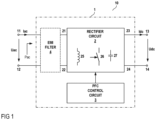
- FIG. 1 schematically illustrates one example of a power converter circuit 10.
- the power converter circuit 10 includes a PFC (power factor correction) rectifier 1.
- the PFC rectifier 1 includes an input 11, 12 configured to receive an input voltage Uac and an input current lac from a power source (not illustrated in Figure 1 ) and an output 13, 14 configured to provide an output voltage Udc and an output current Idc to a load or load circuit (not illustrated in Figure 1 ).
- the PFC rectifier 1 includes a rectifier circuit 2 and a PFC control circuit 3 that is configured to control operation of the rectifier circuit 2.
- an EMI (electromagnetic interference) filter 4 is connected between the input 11, 12 of the PFC rectifier and an input 21, 22 of the rectifier circuit 2.
- An output 23, 24 of the rectifier circuit 2 may form the output 13, 14 of the PFC rectifier 1.
- the input voltage Uac is an alternating voltage such as, for example a sinusoidal voltage.
- the power source providing the alternating input voltage Uac is a power grid, for example.
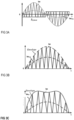
- Figure 2A shows a signal diagram of a sinusoidal input voltage Uac during one period of the sinusoidal input voltage Uac.
- An RMS (Rout Mean Square) value of the input voltage Uac and the amplitude ⁇ ac of the input voltage Uac which is 2 times the RMS value Uac rms , U ⁇ ac 2 ⁇ Uac rms , may vary within a certain range, for example, dependent on the country or the location where the power grid is established.
- Typical RMS values of alternating voltages received from power grids range between 90 Vrms and 265 Vrms.
- a typical frequency of the grid voltages is 50 Hz or 60 Hz.
- the output voltage Udc is a direct voltage and the output current Idc is a direct current.
- the PFC control circuit 3 is configured to control operation of the rectifier circuit 2 in a PFC mode.
- Operating the rectifier circuit 2 in the PFC mode includes operating the rectifier circuit 2 such that that an average input current Iac avg received by the rectifier circuit 2 has a current waveform that is in correspondence with the waveform of the input voltage Uac.
- the average input current Iac avg is a sinusoidal input current when the input voltage Uac is a sinusoidal input voltage.
- the rectifier circuit 2 may be operated in such a way that the average input current Iac avg is in phase with the input voltage Uac.
- the PFC rectifier 1 from the perspective of the power source, is an ohmic load.
- a signal diagram of a sinusoidal average input current Iac avg that is in phase with a sinusoidal input voltage Uac is illustrated in Figure 2B .
- the rectifier circuit is operated such that there is a certain phase shift between the average input current Iac avg and the input voltage Uac.
- the input voltage Uac is a sinusoidal voltage and the rectifier circuit 2 is operated in the PFC mode
- the input power Pac has a sine-square waveform as illustrated in Figure 2c , so that the input power regularly oscillates between a maximum power level and zero.
- the oscillating frequency is twice the frequency of the input voltage Uac.
- the rectifier circuit 2 includes a capacitor 27 to buffer variations of the input power Pac that are associated with the PFC mode. It can be assumed that losses in the PFC rectifier are small as compared to an average input power Pac avg , which is given by an average of the input power over one half-period of the input voltage Uac and the average input current Iac avg . In this case, the output power Pdc approximately equals the average input power Pac avg , Pdc ⁇ Pac avg
- the average input current Pac avg is 50% of a peak input power
- Pac pk denotes the peak input power
- Îac avg denotes an amplitude (a peak) of the average input current Iac avg .
- the peak Îac avg of the average input current Iac avg occurs whenever the voltage level of the input voltage Uac equals ⁇ ac.
- the rectifier circuit has a boost converter topology, so that a voltage level of the output voltage Udc is equal to or higher than the amplitude ⁇ ac of the input voltage, Udc ⁇ ⁇ ac.
- the PFC rectifier 1 is configured to regulate the output voltage Udc in accordance with an output voltage reference Udc ⁇ .
- the output voltage reference Udc ⁇ defines a desired voltage level or setpoint of the output voltage Udc.
- regulating the output voltage Udc in accordance with the output voltage reference Udc ⁇ includes regulating the output voltage such that a voltage level of the output voltage Udc at least approximately equals a voltage level defined by the output voltage reference Udc ⁇ .
- Regulating the output voltage Udc by the PFC rectifier 1 includes regulating the average input power Pac avg , wherein regulating the average input power Pac avg includes regulating the amplitude of the average input current Iac avg . This is explained in detail herein further below.
- the rectifier circuit 2 includes an inductor 25 and an electronic switch 26.
- Controlling operation of the rectifier circuit 2 by the PFC control circuit 3 includes controlling operation of the switch 26, wherein controlling operation of the switch 26 includes operating the switch in an on-state (switched on state) or an off-state (switched off state).
- the inductor 25 and the switch 26 are coupled with each other and coupled to the input 21, 22 in such a way that the input current lac increases and energy is stored in the inductor 25 when the switch 26 is in the on-state, and the input current lac decreases and energy is transferred to the capacitor 26 and the output 23, 24 when the switch 26 is in the off-state.
- the input current lac can be modulated in order to control waveform and amplitude of the average input current Iac avg .
- Different examples of rectifier circuits 2 operating in this way are explained in detail herein further below.
- Figures 3A to 3C Conventional ways for operating a rectifier circuit 2 in a PFC mode are illustrated in Figures 3A to 3C , wherein each of these Figures 3A to 3C illustrates the input current lac and the average input current Iac avg during one period or during one half-period of a sinusoidal average input current Iac avg .
- Figure 3A illustrates operating a PFC rectifier circuit in a triangular current mode (TCM).
- TCM triangular current mode
- the input current lac is modulated such that it alternates in a triangular fashion between a first current level and a second current level.
- the first current level is negative during the positive half-wave of the average sinusoidal input current Iac avg and is positive during the negative half-wave.
- the second level defines a sinusoidal envelope.
- Figure 3B illustrates operating a PFC rectifier in a critical conduction mode (CrCM).
- the input current lac in a triangular fashion, alternates between a first level and a second level, wherein the second level defines a sinusoidal envelope.
- the first level is zero in the critical conduction mode.
- Figure 3C illustrates operating a PFC rectifier in a discontinuous conduction mode (DCM).
- DCM discontinuous conduction mode
- ZVS zero-voltage switching
- the at least one switch may be operated such that the input current lac increases when the switch is in an on-state and decreases when the switch is in an off-state.
- the at least one switch can be operated under ZVS conditions.
- the frequency of the triangular input current lac is, usually, significantly higher than the frequency of the average input current Iac avg and the input voltage Uac.
- the frequency of the input voltage Uac and the alternating average input current Iac avg is 50 Hz or 60 Hz, for example.
- the frequency of the triangular input current lac is several ten kilohertz or even several hundred kilohertz, for example.
- the frequency of the triangular input current lac significantly varies over one half-period of the input voltage Uac and the average input current Iac avg . This frequency variation is dependent, inter alia, on the RMS value of the input voltage Uac.
- Figure 4 schematically illustrates the frequency variation of the triangular input current lac in a PFC rectifier that is operated in TCM and generates a fixed output voltage Udc of 400V.
- Figure 4 illustrates the frequency variation for six different input voltages Uac having RMS values of 90 Vrms, 110 Vrms, 150 Vrms, 180 Vrms, 230 Vrms, and 265 Vrms.
- the higher the input voltage Uac the stronger variations of the frequency of the triangular input current lac.
- the frequency of the triangular input current lac equals the frequency at which the at least one switch in the PFC rectifier is operated. This frequency is also referred to as switching frequency in the following.
- the PFC rectifier 1 may include an EMI filter 4.
- the EMI filter 4 is configured to attenuate electromagnetic interferences that result from a switched mode operation of the at least one switch in the rectifier circuit 2 in order to comply with governmental regulations.
- the lowest occurring switching frequency determines the so-called cut-off frequency of the filter, wherein the lower the cut-off-frequency the larger the physical size of inductors included in the EMI filter.
- a zero-crossing detector is required that detects when the input current lac reaches or crosses zero.
- the zero-crossing detector requires additional circuitry and may complicate the design of the PFC rectifier 1.
- the method 100 according to Figure 5 includes operating the rectifier circuit 2 at a fixed switching frequency (101). Furthermore, the method includes regulating the output voltage comprises regulating the output voltage dependent on at least one operating parameter of the rectifier circuit such that the switch is operated under ZVS conditions (102).
- operating the rectifier circuit 2 at a fixed switching frequency includes operating the switch 26 included in the rectifier circuit 2 at a fixed switching frequency.
- Operating the switch 26 at the fixed switching frequency includes switching on the switch 26 at the fixed switching frequency or switching off the switch 26 at the fixed switching frequency, wherein on-durations or off-durations may vary in order to control the input current lac.
- On-durations are time durations during which the switch 26 is in the one-state and “off-durations” are time durations in which the switch 26 is in the off-state.
- regulating the output voltage dependent on at least one operating parameter of the rectifier circuit such that the switch is operated under ZVS conditions includes adjusting the output voltage reference Udc ⁇ dependent on the at least one operating parameter of the rectifier circuit, and regulating the output voltage of the rectifier circuit such that a voltage level of the output voltage is in accordance with the output voltage reference.
- the output voltage reference Udc ⁇ defines a desired voltage level or setpoint of the output voltage Udc.
- the at least one operating parameter based on which the output voltage reference Udc ⁇ is varied is the RMS value of the input voltage Uac received by the rectifier stage 2.
- One example for varying the output voltage reference Udc ⁇ dependent on the RMS value Uac rms of the input voltage Uac is explained in the following.
- the input current lac has a triangular waveform. In each period, the input current lac increases during a first time period Ton and decreases during a second time period Toff.
- the first time period Ton which may also be referred to as on-time, equals the duration of an on-time (switched on time) of the at least one electronic switch included in the rectifier circuit 2.
- the second time period Toff which may also be referred to as off-time, equals a duration of an off-time (switched off time) of the electronic switch 26 included in the rectifier circuit 2. This is explained in detail herein further below.
- Figure 6 illustrates an operating scenario in which an instantaneous voltage level of the input voltage Uac is positive.
- the input current lac increases during the on-time Ton and decreases during the off-time Toff.
- the input voltage Uac is negative, the input current lac decreases during the on-time, so that the magnitude increases, and increases during the off-time, so that the magnitude decreases.
- ZVS can be achieved when the input current lac crosses zero in each period, in particular, when the current crosses zero before the switch switches on.
- Figure 6 illustrates the input current lac reaching zero in each period.
- ⁇ Iac denotes a peak-to-peak current ripple ⁇ Iac.
- the input current lac crosses zero in each period, and ZVS can be achieved, whenever ⁇ Iac t > 2 ⁇ Iac avg t
- the rectifying circuit 2 of the PFC rectifier 1 operates as a boost converter, so that the voltage level of the output voltage Udc is equal to or higher than the amplitude ⁇ ac of the input voltage.
- m(t) ⁇ 1.
- the input voltage Uac and the average input current Iac avg are in phase.
- ZVS at time instance t wc can be achieved whenever 2 ⁇ Uac rms t ⁇ 2 ⁇ Uac rms t 2 Udc L ⁇ fsw > 2 ⁇ 2 ⁇ Pac avg Uac rms
- the switch 26 in the rectifier circuit 2 can be operated under ZVS conditions throughout the period of the input voltage Uac when the switching frequency fsw is fixed and the output voltage Udc is in accordance with equation (14).
- the output voltage reference Udc ⁇ in accordance with equation (14), is selected (adjusted) as follows, Udc * > Uac rms 3 ⁇ 2 Uac rms 2 ⁇ Pac avg ⁇ 2 ⁇ fsw ⁇ L
- the inductance L and the switching frequency fsw are fixed. According to one example, the inductance L and the switching frequency fsw are selected to meet the following condition, fsw ⁇ L ⁇ Uac _ min rms 2 2 ⁇ Pmax avg so that the denominator in equations (15) and (16) is greater than zero, where Uac_min rms denotes the RMS value of the lowest possible input voltage Uac, and Pmax avg denotes the maximum average input power of the rectifier circuit 2.
- the critical output voltage reference Udc crit ⁇ is the smallest possible output voltage for which the current lac reaches zero in each period.
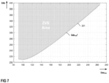
- Figure 7 illustrates the critical output voltage reference Udc crit ⁇ dependent on the RMS value of the input voltage Uac at a given power Pac avg , a given switching frequency fsw, and a given inductance L of the inductor 25 included in the PFC rectifier.
- the diagram shown in Figure 7 is based on an example in which the output power Pac avg is 240 W, the switching frequency fsw is 135 kHz, and the inductance is 50 microhenries ( ⁇ H).
- curve 201 represents the critical output voltage reference Udc crit ⁇ .
- Operating the switch 26 under ZVS can be achieved when the output voltage Udc or the output voltage reference Udc ⁇ is above curve 201.
- the higher the RMS value Uac rms of the input voltage Uac the higher the critical output voltage reference Udc crit ⁇ .
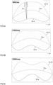
- Figures 8A - 8E illustrate the average input current Iac avg during one half-period of the average input current Iac avg obtained for input voltages with different RMS values, 90 Vrms in Figure 8A , 110 Vrms in Figure 8B , 150 Vrms in Figure 8C , 220 Vrms in Figure 8D , and 265 Vrms in Figure 8E .
- the power Pac avg , the switching frequency fsw, and the inductance L of the inductor 25 included in the PFC rectifier 2 are the same as in the example illustrated in Figure 7 .
- Figures 8A to 8E illustrate upper current ripple boundaries Iac_ub and lower current ripple boundaries Iac_lb.
- the input current lac which is only schematically illustrated in one section of Figure 8A , oscillates between these upper and lower ripple boundaries Iac_ub, Iac_lb.
- the output voltage Udc equals the critical output voltage reference Udc crit ⁇ that can be obtained based on Figure 7 for each of the respective RMS values Uac rms of the input voltage Uac.
- the lower current ripple boundary Iac_lb reaches zero when the average current Iac avg reaches its maximum Îac avg , that is, when the input voltage Uac reaches its maximum ⁇ ac during the respective half-period.
- the lower current ripple boundary Iac_lb is negative, so that the current lac crosses zero in each period of the current lac.
- Figures 8A to 8E illustrate the average input current Iac avg during the positive half-period of the average input current Iac avg .
- the situation in the negative half-period can be obtained by mirroring the diagrams shown in Figures 8A to 8E on the axis representing an input current of zero.
- the lower current ripple boundaries illustrated in Figures 8A to 8E become upper current ripple boundaries and the upper current ripple boundaries illustrated in Figures 8A to 8E become lower current ripple boundaries.
- the output voltage reference Udc ⁇ is adjusted dependent on at least one operating parameter of the rectifier circuit 2.
- operating parameters that affect the output voltage reference Udc ⁇ are the RMS value Uac rms of the input voltage Uac and the average input power Pac avg .
- the output voltage reference Udc ⁇ equals the critical output voltage reference Udc crit ⁇ when the average input power or the output power equals the maximum power Pmax. The latter may include that the input current lac reaches zero when the input voltage Uac reaches its maximum, but may not cross zero.
- the output voltage reference Udc ⁇ is always higher than the critical output voltage reference Udc crit ⁇ , so that the input current lac crosses zero in each period.
- the rectifier circuit 2 may be implemented in various ways. Some examples for implementing the rectifier circuit 2 are explained in the following.
- FIG 9 illustrates one example of the rectifier circuit 2 in greater detail.
- the rectifier circuit 2 includes a Totem pole dual boost PFC rectifier topology or, in short, Totem pole topology.
- the inductor 25 of the rectifier circuit 2 is connected between the input 21, 22 of the rectifier circuit 2 and a tap 26T of a first half-bridge, which may also be referred to as switch half-bridge. More specifically, the inductor 25 is connected between one of the input nodes 21, 22 and the tap 26T. In the example shown in Figure 9 , the inductor 25 is connected between the first input node 21 and the tap 26T. This, however, is only an example. According to another example (not illustrated), the inductor 25 is connected between the second input node 22 and a tap 28T of a rectifier half-bridge explained in the following.
- the output capacitor 27 is connected between the output nodes 23, 24.
- the switch half-bridge 26 includes a first switch 26H, which is also referred to as high-side switch in the following, and a second switch 26L, which is also referred to as low-side switch in the following.
- the high-side switch 26H and the low-side switch 26L are connected in series between the output nodes 23, 24 of the rectifier circuit 2 and are connected with one another at the tap 26T.
- each of the high-side switch 26H and the low-side switch 26L includes a rectifier element that is configured to conduct when a voltage across the respective switch 26H, 26L has a certain polarity.
- the rectifier element is represented by a diode in the example shown in Figure 9 .
- the high-side switch 26H and the low-side switch 26L may be implemented as a MOSFET, so that the rectifier element may be formed by the body diode of the respective MOSFET. This, however, is only an example. Any other type of electronic switch with an internal rectifier element or any other type of electronic switch having an external rectifier element connected in parallel thereto may be used as well.
- high-side and low-side switches 26H, 26L include HEMTs (High Electron Mobility Transistors, IGBTs (Insulated Gate Bipolar Transistors), or cascode circuits with a normally-on transistor and a normally-off transistors.
- HEMTs High Electron Mobility Transistors
- IGBTs Insulated Gate Bipolar Transistors
- cascode circuits with a normally-on transistor and a normally-off transistors.
- the high-side switch 26H and the low-side switch 26L may be connected between the tap 26T and the first and second output nodes 23, 24 such that the rectifier element of the high-side switch 26H conducts when an electrical potential at the tap 26T is higher than the electrical potential at the first output node 23 and such that the rectifier element of the low-side switch 26L conducts when the electrical potential at the tap 26T is lower than the electrical potential at the second output node 24.
- the rectifier circuit 2 further includes a second half-bridge 28 that is connected between the first and second output nodes 23, 24 and includes a tap 28T that is connected to the input.
- the tap 28T is connected to the second input node 22.
- the second half-bridge 28 which may also be referred to as rectifier half-bridge, includes two rectifier elements connected in series between the first and second output nodes 23, 24 and connected with each other at the tap 28T.
- a first rectifier element 28H is connected between the tap 28T and the first output node 23 and is also referred to as high-side rectifier element in the following
- a second rectifier element 28L is connected between the second output node 24 and the tap 28T and is also referred to as low-side rectifier element in the following.
- the rectifier elements 28H, 28L are pn diodes in the example shown in Figure 9 . However, these rectifier elements may be implemented as Schottky diodes as well.
- an electronic switch (not shown in Figure 9 ) is connected in parallel with each of the high-side element 28H and the low-side rectifier element 28L and is switched on by a respective drive circuit whenever the respective rectifier element is forward biased.
- the high-side rectifier element 28H is connected between the tap 28T of the second half-bridge 28 and the first output node 23 in such a way that the high-side rectifier element 28H conducts when the electrical potential at the tap 28T is higher than the electrical potential at the first output node 23, and the low-side rectifier element 28L is connected between the second output node 24 and the tap 28T such that the low-side rectifier element 28L conducts when the electrical potential at the second output node 24 is higher than the electrical potential at the tap 28T.
- the PFC control circuit 3 is configured to control operation of the rectifier circuit 2 by providing drive signals S26H, S26L received by the high-side switch 26H and the low-side switch 26L. Examples of the PFC control circuit 3 are explained in detail herein further below.
- the amplitude and the waveform of the average input current Iac avg can be adjusted by suitably controlling on-times and off-times of an electronic switch included in the rectifier circuit.
- the rectifier circuit 2 according to Figure 9 includes two switches, high-side switch 26H and low-side switch 26L. Dependent on the polarity of the input voltage Uac one of the high-side switch 26H and low-side switch 26L acts as a control switch for controlling the input current lac and the other one of the high-side switch 26H and low-side switch 26L acts as a rectifier element.
- the low-side switch 26L acts as the control switch for controlling the input current lac and the high-side switch 26H acts as a rectifier element.
- the high-side switch 26H may be switched off throughout the positive half-period of the input voltage Uac or may be switched on and off complementarily to the low-side switch 26L.
- the input current lac increases whenever the low-side switch 26L is switched on and the input current lac flows via the inductor 25, the low-side switch 26L and the low-side rectifier element 28L.
- the input current through the inductor 25 decreases and continues to flow via the high-side switch 26H or the parallel rectifier element, the output capacitor 27 and the load circuit (not shown), and the low-side rectifier element 28L.
- the high-side switch 26H acts as the control switch for controlling the input current lac and the low-side switch 26L acts as a rectifier element.
- the low-side switch 26H may be switched off throughout the negative half-period of the input voltage Uac or may be switched on and off complementarily to the low-side switch 26L.
- the average input current is negative.
- the input current lac decreases (towards more negative current levels) whenever the high-side switch 26H is switched on and the input current lac flows via the high-side rectifier element 28H, the high-side switch 26H and the inductor 25.
- the input current through the inductor 25 increases (towards more positive current levels) and continues to flow via the low-side switch 26H or the parallel rectifier element, the output capacitor 27 and the load circuit (not shown), and the high-side rectifier element 28L.
- the PFC control circuit 3 controls the duty cycle d26 of the switch acting as the control switch at the respective time instance.
- Each of the high-side switch 26H and the low side switch 26L includes an output capacitance, which is a capacitance parallel to the respective switch.
- the output capacitance is charged whenever the respective switch 26H, 26L switches off and a voltage across the switch 26H, 26L increases.
- the output capacitance is discharged, so that the voltage across the switch 26H, 26L decreases and the switch 26H, 26L can be switched on under ZVS conditions.
- Figure 10 shows a rectifier circuit 2 which is a modification of the converter stage according to Figure 9 .
- the topology of the rectifier circuit 2 according to Figure 10A may be referred to as double boost PFC rectifier or, in short, double boost topology.
- the rectifier circuit 2 according to Figure 10 is different from the rectifier circuit 2 according to Figure 9 in that a first half-bridge, which has a first tap 261T connected to the inductor 25, includes a first low-side switch 261L and a first high-side rectifier element 281H (instead of a high-side switch and a low-side switch) and in that a second half-bridge, which has a second tap 262T connected to the second input node 22, includes a second low-side switch 262L and a second high-side rectifier element 282H (instead of a high-side rectifier element and a low-side rectifier element).
- the first high-side rectifier 281H is connected between the tap 261T and the first output node 23 such that it conducts when the electrical potential at the first tap 261T is higher than the electrical potential at the first output node 23.
- the second high-side rectifier element 282H is connected between the second tap 262T and the first output node 24 such that it conducts when the electrical potential at the tap 262T is higher than the electrical potential at the first output node 23.
- the first and second low-side switches 261L, 262L may each include a rectifier element (freewheeling element) that is configured to conduct when a voltage across the respective switch 261L, 262L has a certain polarity.
- a rectifier element freewheeling element
- the first low-side switch 261L may be connected between the first tap 261T and the second output node 24 such that the rectifier element of the first low-side switch 261L conducts when an electrical potential at the first tap 261T is lower than the electrical potential at the second output node 24, and the second low-side switch 262L of the second half-bridge may be connected between the second tap 262T and the second output node 24 such that the rectifier element of the second low-side switch 262L conducts when an electrical potential at the second tap 262T is lower than the electrical potential at the second output node 24.
- one of the first and second low-side switches 261L, 262L acts as a control switch for controlling the input current lac and the other one of the first and second low-side switches 261L, 262L acts as a rectifier element.
- the first low-side switch 261L acts as the control switch for controlling the input current lac and the second low-side switch 262L acts as a rectifier element.
- the second low-side switch 262L may be switched off throughout the positive half-period of the input voltage Uac or may be switched on throughout the positive half-period of the input voltage Uac.
- the input current lac increases whenever the first low-side switch 261L is switched on and the input current lac flows via the inductor 25, the first low-side switch 261L and the second low-side switch 262L or its rectifier element.
- the input current through the inductor 25 decreases and continues to flow via the first high-side rectifier element 281H, the output capacitor 27 and the load circuit (not shown), and the second low-side switch 262L or its rectifier element.
- the second low-side switch 262L acts as the control switch for controlling the input current lac and the first low-side switch 261L acts as a rectifier element.
- the first low-side switch 261L may be switched off throughout the negative half-period of the input voltage Uac or may be switched on and throughout the negative half-period of the input voltage Uac.
- the average input current is negative.
- the input current lac decreases (towards more negative current levels) whenever the second low-side switch 26H is switched on and the input current lac flows via the second low-side switch 262L, the first low-side switch 261L or its rectifier element and the inductor 25.
- the second low-side switch 262L switches off, the input current through the inductor 25 increases (towards more positive current levels) and continues to flow via the second high-side rectifier element 282H, the output capacitor 27 and the load circuit (not shown), and the high-side rectifier element 28L, and the first low-side switch 261L or its rectifier element.
- the PFC control circuit 3 is configured to control operation of the rectifier circuit 2 by providing drive signals S261L, S262L received by the first and second low-side switches 261L, 262L.
- the PFC control circuit 3 controls the duty cycle d26 of the switch acting as the control switch.
- Figure 11 shows a rectifier circuit 2 with a boost converter topology according to another example.
- the topology of the rectifier circuit 2 shown in Figure 11 may be referred to as H4-PFC rectifier topology or double boost PFC rectifier with bidirectional switch topology.
- the rectifier circuit 2 includes two half-bridges that are each connected between the first output node 23 and the second output node 24.
- Each of these half-bridges includes two rectifier elements 283H, 283L, 284H, 284L connected in series between the first and second output nodes 23, 24.
- the rectifier elements 283H, 283L, 284H, 284L of each of the first and second half-bridges are connected to one another at a respective tap 283T, 284T, wherein the tap 283 of the first half-bridge is connected to the inductor 25 and the tap 284T of the second half-bridge is connected to one of the input nodes 21, 22.
- the inductor 25 is connected to the first input node 21 and the tap 284T of the second half-bridge 283 is connected to the second input node 22.
- the half-bridges may be implemented with passive rectifier elements such as, for example, pn diodes (as illustrated) or Schottky diodes (not illustrated). Additionally, a respective switch (not shown) may be connected in parallel with each of the rectifier elements 283H, 283L, 284H, 284L, wherein the switch is driven by a respective drive circuit (also not shown) in such a way that the switch switches on when the respective rectifier element is forward biased.
- passive rectifier elements such as, for example, pn diodes (as illustrated) or Schottky diodes (not illustrated).
- a respective switch may be connected in parallel with each of the rectifier elements 283H, 283L, 284H, 284L, wherein the switch is driven by a respective drive circuit (also not shown) in such a way that the switch switches on when the respective rectifier element is forward biased.
- the rectifier elements are connected between the first and second output nodes 23, 24 and the taps 283T, 284T such that a high-side rectifier element 283H of the first half-bridge conducts when the electrical potential at the tap 283T is higher than the electrical potential at the first output node 23; the low-side rectifier element 283L of the first half-bridge conducts when the electrical potential at the second output node 24 is higher than the electrical potential at the tap 283T; a high-side rectifier element 284H of the second half-bridge when an electrical potential at the tap 284T is higher than the electrical potential at the first output node 23; and a low-side rectifier element 284L of the second half-bridge 283 conducts when the electrical potential at the second output node 24 is higher than the electrical potential at the tap 284T.
- the rectifier circuit 2 includes a switch 263 that is connected between the taps 283T, 284T and that is controlled by the PFC control circuit 3 through a respective drive signal S263.
- the switch 263 is a bidirectionally blocking switch, for example.
- the switch 263 acts as a control switch, wherein the PFC control circuit, for controlling the input current lac, adjusts the duty-cycle of the control switch 263.
- the PFC control circuit 3 is configured to control operation of the rectifier circuit 2 by providing a drive signal S263 received by switch 263.
- the PFC control circuit 3 controls the duty cycle d26 of switch 263.
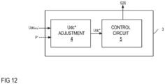
- PFC control circuit 3 that is configured to control operation of the rectifier circuit 2 is explained with reference to Figures 12 and 13 in the following. It should be noted that these figures represent a functionality of the PFC control circuit 3 rather than a specific implementation.
- the PFC control circuit 3 may be implemented in various ways. According to one example, the PFC control circuit 3 is implemented using dedicated circuitry. According to another example, the PFC control circuit 3 includes a microcontroller and a memory that includes instructions (software) executed by the microcontroller.
- the PFC control circuit 3 includes an output voltage reference circuit 4 that is configured to output the output voltage reference Udc ⁇ .
- the output voltage reference circuit 4 is configured to calculate the output voltage reference Udc ⁇ in accordance with any one of equations (18a), (18b), and (19).
- the output voltage reference circuit 4 receives a measured RMS value Uac rms ', which is obtained by measuring the input voltage Uac and represents the RMS value of the input voltage Uac.
- the output voltage reference circuit 4 further receives a measured power P'.
- the measured power P' represents the average input power Pac avg or the output power Pdc and is obtained by measuring the input power Pac or the output power Pdc.
- Information on the switching frequency fsw and the inductance are included in the output voltage reference circuit 4.
- the output voltage reference circuit 4 may include any kind of circuit that is configured to provide the output voltage reference Udc ⁇ dependent on the measured RMS value Uac rms ' and the measured power P' in accordance with any one of equations (18a), (18b), and (19).
- This circuit may include a look-up table, a calculation circuit, or the like.
- a control circuit 5 receives the output voltage reference Udc ⁇ and is configured to control operation of the rectifier circuit 2 by generating at least one drive signal S26.
- Drive signal S26 in Figure 12 represents any one of the drive signals S26H, S26L illustrated in Figure 9 , S2611, S262L illustrated in Figure 10 , or S263 illustrated in Figure 11 for driving the respective switch(es).
- Figure 13 illustrates one example of the control circuit 5 in greater detail. It should be noted that the control circuit 5 according to Figure 13 is only an example. Basically, any kind of control circuit may be used that is configured to control operation of a rectifier circuit in a PFC rectifier in a PFC mode such that an output voltage is in accordance with an output voltage reference.
- the control circuit 5 includes an output voltage controller (output voltage regulator) 5U that receives the output voltage reference Udc ⁇ and a measured output voltage Udc' and is configured to provide an inductor current reference I25 ⁇ .
- the measured output voltage Udc' represents the instantaneous voltage level of the output voltage Uac and can be obtained by measuring the output voltage Uac using any kind of voltage measurement circuit.
- the inductor current reference I25 ⁇ represents a desired current through the inductor 25.
- control circuit 5 includes a current controller 51 that receives the inductor current reference I25 ⁇ and a measured inductor current 125' and is configured to generate the drive signal S26 for controlling the control switch.
- the measured inductor 125' represents the instantaneous current level of the inductor current 125' and can be obtained by measuring the inductor current 125 using any kind of current measurement circuit.
- the measured inductor 125' current represents an average of the instantaneous current level of the inductor current 125' during one drive cycle of the switch 26.
- the output voltage controller 5U includes a subtractor 51 that subtracts a measured output voltage Udc' from the output voltage reference Udc ⁇ and provides an error signal Udc_err that represents a difference between the output voltage reference Udc ⁇ and the measured output voltage Udc'.
- a filter (regulator) 52 receives the error signal Ucd_err and provides a filter output signal S52 based on the error signal Ucd_err.
- Filter (regulator) 52 has one of a proportional (P), proportional-integral (PI), or proportional-integral-derivative (PID) characteristic, for example.
- the filter output signal S52 represents a current 127 (see Figures 9 , 10 , 11 ) into the output capacitor 27.
- An adder 53 adds a measured output current Idc' to the filter output signal S52 and provides an adder output signal S53.
- the adder output signal S53 represents the overall current of the rectifier circuit 2, that is, the current through the inductor 25.
- the measured output current Idc' represents the instantaneous current level of the output current Idc and can be obtained by measuring the output current Idc Uac using any kind of current measurement circuit.
- a multiplier 54 multiplies the adder output signal S53 with the output voltage reference Udc ⁇ .
- An output signal P ⁇ of the multiplier represents a power reference P ⁇ , wherein power reference P ⁇ represents a desired output power Pdc or a desired average input power.
- An optional limiter 55 limits the power reference P ⁇ such that the power reference P ⁇ does not exceed the maximum power Pmax.
- a divider 56 receives the power reference P ⁇ and divides the power reference by 1 2 U ⁇ ac ′ 2 , where ⁇ ac' denotes the measured amplitude of the input voltage Uac, wherein the measured amplitude ⁇ ac' represents the amplitude of the input voltage Uac and may be obtained by measuring the input voltage Uac.
- An output signal G ⁇ of the divider represents a desired conductance of the rectifier circuit 2.
- a further multiplier 57 multiplies the desired conductance G ⁇ with the measured input voltage Uac'.
- the measured input voltage Uac' represents the instantaneous voltage level of the input voltage Uac and can be obtained by measuring the input voltage Uac using any kind of voltage measurement circuit.
- An output signal of the further multiplier 57 represents the inductor current reference I25 ⁇ .
- the current controller 51 that is configured to regulate the inductor current 251 includes a further subtractor 58 that is configured to subtract the measured inductor current 125' from the inductor current reference I25 ⁇ to provide an error signal I25_err that represents a difference between the inductor current reference I25 ⁇ and the measured inductor current 125'.
- a further filter (regulator) 59 receives the current error signal I25_err and provides a filter output signal S59 based on the current error signal I25_err. Further filter (regulator) 59 has one of a proportional (P), proportional-integral (PI), or proportional-integral-derivative (PID) characteristic, for example.
- the filter output signal S59 represents an inductor voltage reference Ul ⁇ , which is a desired voltage Ul across the inductor 25.
- An adder 60 adds the inductor voltage reference Ul ⁇ and the measured input voltage Uac', wherein an adder output signal represents a switch node voltage reference Ut ⁇ , which is a desired voltage level of a voltage Ut at the circuit node between the inductor 25 and the control switch.
- An optional limiter 56 limits the switch node voltage reference Ut ⁇ such that the switch node voltage reference Ut ⁇ does not exceed the measured input voltage Udc'.
- the switch node voltage Ut is adjusted by a switched-mode operation of the control switch.
- the switch node voltage Ut is zero when the control switch is in the on-state and the switch node voltage Ut essentially equals the output voltage Udc when the control switch is in the off-state.
- the duty-cycle d26 is obtained by dividing the switch node voltage reference Ut ⁇ by the measured output voltage Udc' by a divider 62.
- a PWM modulator 63 receives the duty-cycle d26 and is configured to generate the drive signal S26 for controlling the control switch.
- the control switch changes when the polarity of the input voltage Uac changes.
- the PWM modulator 63 may receive the measured input voltage Uac' in order to decide which of the switches (S26L or S26H in Figure 9 or S261L or S262L in Figure 10 ) is the control switch at the respective time instance.
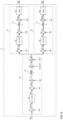
- FIG 16 illustrates a rectifier circuit 2 according to another example.
- the rectifier circuit 2 according to Figure 14 includes several rectifier circuit stages 2 1 , 2 n that are connected in parallel between the input 21, 22 and the output 23, 24.
- each of these rectifier stages 21, 22 is in accordance with one of the examples illustrated in Figures 9 - 11 , wherein the rectifier stages 2 1 , 2 n share the output capacitor 27.
- the rectifier circuit 2 according to Figure 2 includes two rectifier stages 2 1 , 2 n connected in parallel. This, however, is only an example. It is also possible to implement the rectifier circuit 2 with more than two rectifier stages 2 1 , 2 n connected in parallel.
- the PFC control circuit 3 is configured to control operation of both rectifier stages 2 1 , 2 n .
- the PFC control circuit 3 may be implemented as explained with reference to Figure 12 and include an output voltage reference circuit 4 that is configured to provide the output voltage reference Udc ⁇ .
- the output voltage reference circuit 4 may be configured to generate the output voltage reference Udc ⁇ in accordance with one of equations (18a), (18b), (18c), wherein Pmax in equations (18a) and (18b) is the maximum power of one rectifier stage 2 1 , 2 n and P in equation (19) is the power of one converter stage.
- the rectifier stages 2 1 , 2 n are implemented with identical components and operated such that each converter stage 2 1 , 2 n provides an equal share of 1/n of the overall output power of the PFC rectifier, wherein n denotes the number of rectifier stages connected in parallel.
- the power P according to equation (19) may be obtained by measuring the average input power or the output power of one of the converter stages 2 1 , 2 n , or may be obtained by measuring an overall average input power or an overall average output power of the rectifier circuit 2 and dividing the measurement result by n.
- the PFC control circuit 5 may include a control circuit 5 of the type explained with reference to Figure 13 .
- One example of such control circuit is illustrated in Figure 16 .
- the control circuit 5 according to Figure 16 is different from the control circuit according to Figure 13 in that it includes n current controllers 5I 1 , 5I n that each receive the inductor current reference I25 ⁇ from the output voltage regulator 5U.
- Each of the current controllers 5I 1 , 5I n is configured to generate a drive signal S26i, S26 n for the control switch in a respective one of the rectifier stage 2 1 , 2 n .
- Each of the current controllers 5I 1 , 5I n may be implemented in the same way as the current controller 51 illustrated in Figure 13 .
- like signals and circuit elements as in the example shown in Figure 13 are denoted with the same reference numbers, wherein subscript "1" has been added to the signals and circuit elements of a first one 5I 1 and subscript "2" has been added to the signals and circuit elements of a second one 5I 2 of current the current controller 5I 1 , 5I 2 .
- the current controllers 5I 1 , 5I 2 are configured to operate the two rectifier stages 2 1 , 2 2 at the same switching frequency fsw and may be configured to operate the rectifier stages 2 1 , 2 2 in an interleaved fashion. The latter, however, is only an example.
- the power converter circuit 10 in addition to the PFC rectifier 1, includes a DC-DC converter 6.
- the DC-DC converter 6 includes an input 61, 62, that is connected to the output 13, 14 of the PFC rectifier 1 and is configured to receive the output voltage Udc from the PFC rectifier 1.
- the output voltage Udc of the PFC rectifier 1 may also be referred to DC link voltage.
- the DC-DC converter 6 is configured to provide an output voltage Uo and an output current Io based on the DC link voltage Udc and the output current Idc (DC link current Idc) received from the PFC rectifier 1.
- any type of isolated or non-isolated DC-DC converter may be used to implement DC-DC converter 6 according to Figure 10 .
- An "isolated" DC-DC converter is a DC-DC converter that includes a galvanic isolation between the input 61, 62 and the output 63, 64, wherein the galvanic isolation is provided by a transformer, for example.
- a “non-isolated” DC-DC converter is a DC-DC converter that does not include a galvanic isolation between the input 61, 62 and the output 63, 64.
- the DC-DC converter 6 may be configured to provide a regulated output current Io based on the DC link voltage Udc and the DC link current Idc received from the PFC rectifier 1, or may be configured to provide a regulated output current Io based on the DC link voltage Udc or the DC link current Idc.
- a regulated output current Io may be used for charging a battery, for example.
- a regulated output voltage may be used for supplying any kind of DC load such as, for example, a monitor, a computer, or the like.
- the DC-DC converter 6 includes a first converter stage 7 that is configured to receive the DC link voltage Udc and the DC link current Idc and generate an intermediate voltage Uint and an intermediate current lint based on the DC link voltage and the DC link current Idc. Furthermore, the DC-DC converter 6 includes a second converter stage 8 that is configured to receive the intermediate voltage Uint and the intermediate current lint from the first converter stage 7 and provide the output voltage Uo and the output current Io based on the intermediate voltage Uint and the intermediate current lint.
- one of the first and second converter stages 7, 8 is a non-regulated converter stage and the other one of the first and second converter stages 7, 8 is a regulated converter stage.
- the first converter stage 7 is a non-regulated converter stage, that is, the first converter stage includes a non-regulated converter.
- each of m and n is an integer selected from between 2 and 10, for example.
- m and n are selected such that the first converter stage 7 is a buck stage, so that DC-DC Uint/Udc ⁇ 1.
- the first converter stage 7 includes an isolated resonant converter.
- the second converter stage 8 includes a buck converter with a non-isolated topology, for example.
- the second converter stage 8 includes a regulated converter, so that either the output current Io or the output voltage Uo is regulated.
- the output voltage Vo is selected from between 5V and 50V, in particular, fro, between 10V and 30V, for example.
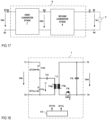
- Figure 18 illustrates one example of the first converter stage 7.
- the first converter stage 7 includes a hybrid flyback converter, which is one example of a resonant converter.
- the hybrid flyback converter according to Figure 18 includes a half-bridge with a high-side switch 711H and a low-side switch 711L connected between a first input node 71 and a second input node 72 of the first converter stage 7.
- the circuit symbols of the high-side and low-side switches 711H, 711L in Figure 12 represent HEMTs such as GaN-HEMTs. This, however, is only an example.
- the high-side and low-side switch 711H, 711L of the half-bridge may be implemented using any kind of conventional electronic switch.
- the half-bridge 711H, 711L is controlled by a control circuit 717 that generates drive signals S711H, S711L received by the high-side and low-side switches 711H, 711L.
- control circuit 717 operates the half-bridge 711H, 711L at a fixed switching frequency such that a voltage U7 with a rectangular signal waveform and a fixed frequency is generated across the low-side switch 711L.
- a series circuit including a capacitor 713 and a primary winding 714p of a transformer 714 is connected in parallel with the low-side switch 711L and receives the rectangular voltage U7.
- the hybrid flyback converter includes a secondary winding 714s of the transformer 714, wherein the secondary winding 714s is inductively coupled with the primary winding 714p.
- a rectifier circuit 715, 716 is connected in parallel with the secondary winding 714s.
- the rectifier circuit includes a capacitor 715 and a rectifier element 716 connected in series with the capacitor 715.
- the intermediate voltage Uint is available across the capacitor 715.
- the rectifier element 716 may be an active rectifier element (as illustrated) or a passive rectifier element.
- a ratio between a voltage level of the DC link voltage Udc and the intermediate voltage Uint is dependent on a winding ratio of the transformer 714.
- the primary winding 714p and the secondary winding 714s have opposite winding senses in the hybrid flyback converter.
- the hybrid flyback converter includes an output capacitor 715 connected between the output nodes 73, 74.
- Figure 19 illustrates another example of a resonant converter.
- the resonant converter includes a transformer 721 with a primary winding 721p and the secondary winding 721s, wherein the primary winding 721p and the secondary winding 721s have the same winding sense and are inductively coupled.
- a capacitor 722 is connected in series with the primary winding 721p.
- a series circuit including the primary winding 721p and the capacitor 722 is coupled to the input 71, 72 via a first full-bridge circuit that includes two half-bridges 723, 724. More specifically, a first circuit node of the series circuit is connected to a tap 723T of a first half-bridge and a second circuit node of the series circuit is connected to a tap 724T of a second half-bridge 724.
- Each of the first and second half-bridges includes a high-side switch 723H, 724H and a low-side switch 723L, 724L that are connected at the tap 723T, 724T and is connected between the input nodes 71, 72.
- the first and second half-bridges 723, 724 are controlled by a control circuit 727 that generates drive signals S723H, S723L, S724H, S724L for the high-side and low-side switches of the half-bridges 723, 724.
- the control circuit 727 is configured to control operation of the full-bridge such that an alternating voltage that alternates between +Udc and -Udc is generated based on the DC link voltage Udc across the series circuit with the capacitor 722 and the primary winding 721p.
- the secondary winding 721s is connected to the output 73, 74 through a second full-bridge with two half-bridges 725, 726.
- Each of the half-bridges 725, 726 is connected between the output nodes 73, 74 and includes a high-side switch 725H, 726H and a low-side switch 725L, 726L that are connected at a respective tap 725T, 726T.
- the secondary winding 721a is connected between the taps 725T, 726T of the half-bridges 725, 726.
- the second full-bridge is operated by the control circuit 726 synchronously with the first full-bridge, so that the second full-bridge 727 acts as an active rectifier for generating the intermediate voltage Uint.
- the intermediate voltage Uint is available across an output capacitor 728.
- Figure 20 illustrates one example of the second converter stage 8.
- the second converter stage 8 includes a buck converter.
- the buck converter includes a series circuit with an electronic switch 84, an inductor 85, and a capacitor 86, wherein the series circuit is connected between input nodes 81, 82 of the buck converter.
- the intermediate voltage Unit is available between the input nodes 81, 82.
- the output voltage Uo is available across the capacitor 86.
- a rectifying element 87 is connected in parallel with a series circuit including the inductor 85 and the capacitor 86.
- the rectifier element may be an active rectifier element (as illustrated) or a passive rectifier element.
- the electronic switch 84 and the active rectifier element may be implanted as HEMTs. This, however, is only an example. Any other kind of electronic switch may be used as well.
- a control circuit 88 is configured to control operation of the electronic switch 84 dependent either on a measured the output current Io' or a measured output the output voltage Vo in order to either regulate the output current Io or the output voltage Vo. This is commonly known so that no further explanation is required in this regard.
- Example 1 A method, including: operating a rectifier circuit in a PFC mode, wherein operating the rectifier circuit in the PFC mode includes: regulating an output voltage of the rectifier circuit, wherein regulating the output voltage includes operating a switch of the rectifier circuit at a fixed switching frequency, and wherein regulating the output voltage includes regulating the output voltage dependent on at least one operating parameter of the rectifier circuit such that the switch is operated under ZVS conditions.
- Example 2 The method of example 1, wherein regulating the output voltage dependent on at least one operating parameter of the rectifier circuit such that the switch is operated under ZVS conditions includes: adjusting an output voltage reference dependent on the at least one operating parameter of the rectifier circuit; and regulating the output voltage of the rectifier circuit such that a voltage level of the output voltage is in accordance with the output voltage reference.
- Example 3 A method, including: operating a rectifier circuit in a PFC mode, wherein operating the rectifier circuit in the PFC mode includes: adjusting an output voltage reference dependent on at least one operating parameter of the rectifier circuit; and regulating an output voltage of the rectifier circuit such that a voltage level of the output voltage is in accordance with an output voltage reference, and wherein regulating the output voltage comprises operating a switch of the rectifier circuit at a fixed switching frequency (fsw).
- fsw fixed switching frequency
- Example 4 The method according to example 1 or 3, wherein the at least one operating parameter includes an RMS value of an alternating input voltage received by the rectifier circuit.
- Example 5 The method according to example 5, wherein the at least one operating parameter further includes one of an average input power or an output power of the rectifier circuit.
- Example 6 The method according to any one of examples 1 to 5, wherein the rectifier circuit includes an inductor having an inductance, and wherein adjusting the output voltage reference further includes adjusting the output voltage reference dependent on the inductance and the fixed switching frequency.
- Example 7 The method according to example 6, wherein operating the switch under ZVS conditions includes adjusting a duty-cycle of the switch in such a way that a current through the inductor crosses zero in each drive cycle of the switch.
- Pmax denotes one of the maximum average input power and the maximum output power of the rectifier circuit 2
- Uac rms denotes the RMS value of the input voltage
- fsw denotes the switching frequency
- L denotes an inductance of an inductor in the rectifier circuit
- p denotes a proportionality factor, wherein 1 ⁇ p ⁇ 1.2.
- P denotes one of the average instantaneous input power Pac avg and the instantaneous output power Pdc
- Uac rms denotes the RMS value of the input voltage
- fsw denotes the switching frequency
- L denotes an inductance of an inductor in the rectifier circuit
- q denotes a proportionality factor, wherein 1 ⁇ q ⁇ 1.2.
- Example 11 The method according to any one of examples 1 to 10, wherein the rectifier circuit includes two rectifier stages connected in parallel, and wherein regulating the output voltage includes operating a switch in each of the rectifier stages at the same fixed switching frequency.
- Example 12 The method according to any one of examples 1 to 11, further including: converting the output voltage of the PFC rectifier into a fixed further output voltage or a fixed output current by a DC-DC converter.
- Example 13 The method according to example 12, wherein the DC-DC converter includes a first converter stage and a second converter stage, wherein one of the first and second converter stages is a regulated converter stage and the other one of the first and second converter stages is a non-regulated converter stage.
- Example 14 The method of any one of the preceding examples, wherein the RMS value of the input voltage ranges between 90 Vrms and 265Vrms.
- Example 15 The method of any one of the preceding examples, wherein the output voltage reference is adjusted to be within 210V and 400V.
- Example 16 A PFC control circuit configured to operate a rectifier circuit in a PFC mode, wherein, to operate the rectifier circuit in the PFC mode, the control circuit is configured to adjust an output voltage reference dependent on at least one operating parameter of the rectifier circuit; and regulate an output voltage of the rectifier circuit such that a voltage level of the output voltage is in correspondence with an output voltage reference, and wherein the control circuit, to regulate the output voltage, is configured to operate a switch of the rectifier circuit at a fixed switching frequency.
- Example 17 A power converter circuit, including: a PFC control circuit according to example 16; and a rectifier circuit controlled by the PFC control circuit.
- Example 18 The power converter circuit according to example 76, further including: a DC-DC converter connected downstream the PFC rectifier.
- Example 19 The power converter circuit according to example 17, wherein the DC-DC converter includes a first converter stage and a second converter stage, wherein one of the first and second converter stages is a regulated converter stage and the other one of the first and second converter stages is a non-regulated converter stage.
Landscapes
- Engineering & Computer Science (AREA)
- Power Engineering (AREA)
- Rectifiers (AREA)
Abstract
Description
- This disclosure relates in general to a power conversion method and a power converter circuit. In particular, the invention relates to an AC-DC power conversion method and power converter circuit including a PFC rectifier.
- Power converters that employ AC-DC power conversion are widely used in various kinds of applications such as battery chargers or DC (direct current) power supplies. AC-DC power conversion includes converting power received from an AC (alternating current) power source into DC power. The AC power source is a power grid, for example. Dependent on the country, an AC voltage provided by the power grid may vary between 90 Vrms and 265Vrms, for example. A voltage level of a DC voltage provided by the AC-DC converter is dependent on the specific application in which the power converter is used and may range from several volts to several 10 volts, for example.
- AC-DC power converters may include a PFC (Power Factor Correction) rectifier that is configured to receive the ac power and generate a regulated DC link voltage based on the AC power. At the same time, the PFC rectifier is configured to regulate a waveform of an alternating current received from the AC power source in order to control a power factor.
- The PFC rectifier may include electronic switches. Operating the electronic switches is associated with losses, wherein these losses include switching losses and conduction losses. Switching losses are losses associated with switching on and switching off the switches, and conduction losses (ohmic losses) are losses associated with currents flowing through the switches in an on-state.
- The switching losses can be reduced by operating the electronic switches under ZVS (zero voltage switching) conditions. ZVS includes switching on a respective switch when a voltage across the switch is zero (has decreased to zero). However, conventional strategies for operating a PFC rectifier, such as operating the PFC rectifier in a triangular conduction (or current) mode (TCM), a critical conduction mode (CrCM), or a discontinuous conduction mode (DCM) are associated with a varying switching frequency, which may increase the complexity of EMI (electromagnetic interference) filters.
- There is a need for a method for operating a PFC rectifier in an efficient way.
- One example relates to a method. The method includes operating a rectifier circuit in a PFC mode. Operating the rectifier circuit in the PFC mode includes regulating an output voltage of the rectifier circuit. Regulating the output voltage includes operating a switch of the rectifier circuit at a fixed switching frequency, and regulating the output voltage includes regulating the output voltage dependent on at least one operating parameter of the rectifier circuit such that the switch is operated under ZVS conditions.
- Examples are explained below with reference to the drawings. The drawings serve to illustrate certain principles, so that only aspects necessary for understanding these principles are illustrated. The drawings are not to scale. In the drawings the same reference characters denote like features.
-
Figure 1 schematically illustrates one example of a power converter circuit that includes a PFC rectifier; -
Figures 2A - 2C illustrate signal diagrams of an input voltage, an (average) input current, and an input power of the power converter circuit; -
Figures 3A - 3C show signal diagrams that illustrate conventional ways for operating a PFC rectifier; -
Figure 4 illustrates switching frequency variations in a PFC rectifier operated in accordance with the method according toFigure 3A ; -
Figure 5 illustrates one example of a method for operating a PFC rectifier; -
Figure 6 schematically illustrates an input current of the PFC rectifier; -
Figure 7 illustrates a critical output voltage (a critical output voltage reference) dependent on an RMS value of an input voltage; -
Figure 8A - 8E illustrates upper and lower current ripples boundaries and an average input current at different input voltages and an output current reference selected in accordance withFigure 7 ; -
Figures 9 - 11 illustrate different examples of a rectifier circuit of the PFC rectifier; -
Figure 12 illustrates one example of a PFC control circuit that includes an outputvoltage reference circuit 4 and acontrol circuit 5; -
Figure 13 illustrates one example of the control circuit in detail; -
Figure 14 illustrates a rectifier circuit according to another example; -
Figure 15 illustrates one example of a control circuit that is configured to control operation of the rectifier circuit according toFigure 14 ; -
Figure 16 illustrates one example of a power converter circuit that includes a DC-DC converter connected downstream the PFC rectifier; -
Figure 17 illustrates one example of a DC-DC converter that includes two converter stages; -
Figures 17 - 18 illustrate different examples of the first converter stage; and -
Figure 20 illustrates one example of the second converter stage. - In the following detailed description, reference is made to the accompanying drawings. The drawings form a part of the description and for the purpose of illustration show examples of how the invention may be used and implemented. It is to be understood that the features of the various embodiments described herein may be combined with each other, unless specifically noted otherwise.
-
Figure 1 schematically illustrates one example of apower converter circuit 10. Thepower converter circuit 10 according toFigure 1 includes a PFC (power factor correction)rectifier 1. ThePFC rectifier 1 includes aninput Figure 1 ) and anoutput Figure 1 ). ThePFC rectifier 1 includes arectifier circuit 2 and aPFC control circuit 3 that is configured to control operation of therectifier circuit 2. - Optionally, an EMI (electromagnetic interference)
filter 4 is connected between theinput input rectifier circuit 2. Anoutput rectifier circuit 2 may form theoutput PFC rectifier 1. - The input voltage Uac is an alternating voltage such as, for example a sinusoidal voltage. The power source providing the alternating input voltage Uac is a power grid, for example.
Figure 2A shows a signal diagram of a sinusoidal input voltage Uac during one period of the sinusoidal input voltage Uac. An RMS (Rout Mean Square) value of the input voltage Uac and the amplitude Ûac of the input voltage Uac which is

- The output voltage Udc is a direct voltage and the output current Idc is a direct current.
- The
PFC control circuit 3 is configured to control operation of therectifier circuit 2 in a PFC mode. Operating therectifier circuit 2 in the PFC mode includes operating therectifier circuit 2 such that that an average input current Iacavg received by therectifier circuit 2 has a current waveform that is in correspondence with the waveform of the input voltage Uac. Thus, for example, the average input current Iacavg is a sinusoidal input current when the input voltage Uac is a sinusoidal input voltage. - The
rectifier circuit 2 may be operated in such a way that the average input current Iacavg is in phase with the input voltage Uac. In this case, the PFC rectifier 1, from the perspective of the power source, is an ohmic load. A signal diagram of a sinusoidal average input current Iacavg that is in phase with a sinusoidal input voltage Uac is illustrated inFigure 2B . According to another example, the rectifier circuit is operated such that there is a certain phase shift between the average input current Iacavg and the input voltage Uac. - An input power received at the
input rectifier circuit 2 is operated in the PFC mode, the input power Pac has a sine-square waveform as illustrated inFigure 2c , so that the input power regularly oscillates between a maximum power level and zero. The oscillating frequency is twice the frequency of the input voltage Uac. - An output power Pdc of the rectifier circuit is given by the output voltage Udc multiplied with the output current Idc, Pdc=Udc ·Idc. The
rectifier circuit 2 includes acapacitor 27 to buffer variations of the input power Pac that are associated with the PFC mode. It can be assumed that losses in the PFC rectifier are small as compared to an average input power Pacavg, which is given by an average of the input power over one half-period of the input voltage Uac and the average input current Iacavg. In this case, the output power Pdc approximately equals the average input power Pacavg,
- Furthermore, when the input voltage Uac is a sinusoidal voltage and the average input current Iacavg is a sinusoidal current, the average input current Pacavg is 50% of a peak input power,

- The rectifier circuit has a boost converter topology, so that a voltage level of the output voltage Udc is equal to or higher than the amplitude Ûac of the input voltage, Udc ≥ Ûac. According to one example, the
PFC rectifier 1 is configured to regulate the output voltage Udc in accordance with an output voltage reference Udc∗. The output voltage reference Udc∗ defines a desired voltage level or setpoint of the output voltage Udc. According to one example, regulating the output voltage Udc in accordance with the output voltage reference Udc∗ includes regulating the output voltage such that a voltage level of the output voltage Udc at least approximately equals a voltage level defined by the output voltage reference Udc∗. - Regulating the output voltage Udc by the
PFC rectifier 1 includes regulating the average input power Pacavg, wherein regulating the average input power Pacavg includes regulating the amplitude of the average input current Iacavg. This is explained in detail herein further below. - For controlling the input current lac, the
rectifier circuit 2 includes aninductor 25 and anelectronic switch 26. Controlling operation of therectifier circuit 2 by thePFC control circuit 3 includes controlling operation of theswitch 26, wherein controlling operation of theswitch 26 includes operating the switch in an on-state (switched on state) or an off-state (switched off state). Theinductor 25 and theswitch 26 are coupled with each other and coupled to theinput inductor 25 when theswitch 26 is in the on-state, and the input current lac decreases and energy is transferred to thecapacitor 26 and theoutput switch 26 is in the off-state. In this way, the input current lac can be modulated in order to control waveform and amplitude of the average input current Iacavg. Different examples ofrectifier circuits 2 operating in this way are explained in detail herein further below. - Conventional ways for operating a
rectifier circuit 2 in a PFC mode are illustrated inFigures 3A to 3C , wherein each of theseFigures 3A to 3C illustrates the input current lac and the average input current Iacavg during one period or during one half-period of a sinusoidal average input current Iacavg.Figure 3A illustrates operating a PFC rectifier circuit in a triangular current mode (TCM). In this operating mode, the input current lac is modulated such that it alternates in a triangular fashion between a first current level and a second current level. The first current level is negative during the positive half-wave of the average sinusoidal input current Iacavg and is positive during the negative half-wave. The second level defines a sinusoidal envelope. -
Figure 3B illustrates operating a PFC rectifier in a critical conduction mode (CrCM). In this operating mode, the input current lac, in a triangular fashion, alternates between a first level and a second level, wherein the second level defines a sinusoidal envelope. The first level is zero in the critical conduction mode. -
Figure 3C illustrates operating a PFC rectifier in a discontinuous conduction mode (DCM). In this operating mode, the input current lac may be zero for certain time periods. - Operating a PFC rectifier in TCM, CrCM, or DCM is commonly known, so that no further detailed description is required in this regard. In each of these operating modes, the modulation of the input current lac can be achieved by operating at least one switch in the
rectifier circuit 2 in a PWM fashion. In each of these operating modes, zero-voltage switching (ZVS) of the at least one switch is possible. ZVS includes that during an off-state (switched-off state) of the at least one electronic switch a voltage across the electronic switch decreases to zero, which may help to reduce switching losses. - The at least one switch may be operated such that the input current lac increases when the switch is in an on-state and decreases when the switch is in an off-state. When operating the at least one switch such that the current during the off-state changes is polarity, as in TCM, or decreases to zero, as in CrCM and DCM, the at least one switch can be operated under ZVS conditions.
- It should be noted that in
Figures 3A to 3C the input current lac is only schematically illustrated. The frequency of the triangular input current lac is, usually, significantly higher than the frequency of the average input current Iacavg and the input voltage Uac. The frequency of the input voltage Uac and the alternating average input current Iacavg is 50 Hz or 60 Hz, for example. The frequency of the triangular input current lac is several ten kilohertz or even several hundred kilohertz, for example. - In each of the three conventional operating modes illustrated in
Figure 3A to 3C , the frequency of the triangular input current lac significantly varies over one half-period of the input voltage Uac and the average input current Iacavg. This frequency variation is dependent, inter alia, on the RMS value of the input voltage Uac. -
Figure 4 schematically illustrates the frequency variation of the triangular input current lac in a PFC rectifier that is operated in TCM and generates a fixed output voltage Udc of 400V.Figure 4 illustrates the frequency variation for six different input voltages Uac having RMS values of 90 Vrms, 110 Vrms, 150 Vrms, 180 Vrms, 230 Vrms, and 265 Vrms. As can be seen fromFigure 4 , the higher the input voltage Uac, the stronger variations of the frequency of the triangular input current lac. The frequency of the triangular input current lac equals the frequency at which the at least one switch in the PFC rectifier is operated. This frequency is also referred to as switching frequency in the following. - Referring to the above, the
PFC rectifier 1 may include anEMI filter 4. TheEMI filter 4 is configured to attenuate electromagnetic interferences that result from a switched mode operation of the at least one switch in therectifier circuit 2 in order to comply with governmental regulations. The larger the frequency range of the switched mode operation of the at least one switch, the more complicated is the EMI filter design and the larger is typically the EMI filter. The lowest occurring switching frequency determines the so-called cut-off frequency of the filter, wherein the lower the cut-off-frequency the larger the physical size of inductors included in the EMI filter. Moreover, for operating thePFC rectifier 1 in each of TCM, CrCM, and DCM a zero-crossing detector is required that detects when the input current lac reaches or crosses zero. The zero-crossing detector requires additional circuitry and may complicate the design of thePFC rectifier 1. - There is therefore a need for operating a PFC rectifier in an efficient way, in particular, such that zero-voltage switching (ZVS) of the
switch 26 included in thePFC rectifier 2 can be achieved, and such that a less complicated EMI filter can be used. This is achieved by operating thePFC rectifier 2 in accordance with the method illustrated inFigure 5 . - The
method 100 according toFigure 5 includes operating therectifier circuit 2 at a fixed switching frequency (101). Furthermore, the method includes regulating the output voltage comprises regulating the output voltage dependent on at least one operating parameter of the rectifier circuit such that the switch is operated under ZVS conditions (102). - According to one example, operating the
rectifier circuit 2 at a fixed switching frequency includes operating theswitch 26 included in therectifier circuit 2 at a fixed switching frequency. Operating theswitch 26 at the fixed switching frequency includes switching on theswitch 26 at the fixed switching frequency or switching off theswitch 26 at the fixed switching frequency, wherein on-durations or off-durations may vary in order to control the input current lac. "On-durations" are time durations during which theswitch 26 is in the one-state and "off-durations" are time durations in which theswitch 26 is in the off-state. - According to one example, regulating the output voltage dependent on at least one operating parameter of the rectifier circuit such that the switch is operated under ZVS conditions includes adjusting the output voltage reference Udc∗ dependent on the at least one operating parameter of the rectifier circuit, and regulating the output voltage of the rectifier circuit such that a voltage level of the output voltage is in accordance with the output voltage reference.
- Referring to the above, the output voltage reference Udc∗ defines a desired voltage level or setpoint of the output voltage Udc. According to one example, the at least one operating parameter based on which the output voltage reference Udc∗ is varied is the RMS value of the input voltage Uac received by the
rectifier stage 2. One example for varying the output voltage reference Udc∗ dependent on the RMS value Uacrms of the input voltage Uac is explained in the following. -
Figure 6 schematically illustrates the input current lac during several periods of the input current lac, wherein each of these periods has a duration Tsw, wherein the duration Tsw is the reciprocal of the fixed switching frequency fsw,
- The input current lac has a triangular waveform. In each period, the input current lac increases during a first time period Ton and decreases during a second time period Toff. The first time period Ton, which may also be referred to as on-time, equals the duration of an on-time (switched on time) of the at least one electronic switch included in the
rectifier circuit 2. The second time period Toff, which may also be referred to as off-time, equals a duration of an off-time (switched off time) of theelectronic switch 26 included in therectifier circuit 2. This is explained in detail herein further below. -
Figure 6 illustrates an operating scenario in which an instantaneous voltage level of the input voltage Uac is positive. In this case, the input current lac increases during the on-time Ton and decreases during the off-time Toff. When the input voltage Uac is negative, the input current lac decreases during the on-time, so that the magnitude increases, and increases during the off-time, so that the magnitude decreases. - The equations provided in the following relate to the positive half-period of the input voltage Uac. The dependency of the output voltage reference Udc∗ on different operating parameters that can be obtained from this equations, however, is independent of the polarity of the input voltage Uac.
- Referring to the above, ZVS can be achieved when the input current lac crosses zero in each period, in particular, when the current crosses zero before the switch switches on.
Figure 6 illustrates the input current lac reaching zero in each period. InFigure 6 , ΔIac denotes a peak-to-peak current ripple ΔIac. The input current lac reaches zero in each period when
Figure 2 , may vary over the time, and ΔIac(t) denotes the peak-to-peak current ripple. The input current lac crosses zero in each period, and ZVS can be achieved, whenever
- In the
rectifier circuit 2, theinductor 25 is connected to theinput electronic switch 26 the input voltage Uac is applied toinductor 25, so that a slope of the input current lac is given by

inductor 25. Referring toFigure 6 , the input current lac increases during the on-time Ton of theelectronic switch 26, so that the peak-to-peak current ripple ΔIac can be expressed as
- In the
rectifier circuit 2, the on-time of theelectronic switch 26 is dependent on a modulation index m(t), which is given by the ratio between the instantaneous voltage level of the input voltage Uac and the voltage level of the output voltage Udc,
circuit 2 of thePFC rectifier 1 operates as a boost converter, so that the voltage level of the output voltage Udc is equal to or higher than the amplitude Ûac of the input voltage. Thus m(t) ≥ 1. In this case, the on-time Ton is dependent on the modulation index m(t) as follows,
- Based on equation (8) it can be seen that the lower the input voltage level Uac(t) relative to the output voltage level Udc, the longer the duration of the on-time. Based on equations (6a), (7) and (8), the peak-to-peak current ripple ΔIac can be expressed as

- It can be shown that in view of operating the
switch 26 under ZVS conditions the operating scenario in which the magnitude of the average input current Iacavg reaches the peak value Îacavg is most critical. Considering equation (2), the peak value Îacavg of the average input current Iacavg is given by
- When the input voltage Uac is a sinusoidal voltage,


- Let twc be the time instance at which the average input current Iacavg reaches the peak value, so that Iacavg(twc) = Îacavg. Considering equation (4b), ZVS at time instance twc can be achieved whenever

- For the purpose of explanation it is assumed that the input voltage Uac and the average input current Iacavg are in phase. In this case, the input voltage Uac reaches its peak Ûac at time instance twc, that is, Uac(t)=Ûac.
- Considering equations (6b) and (10), the peak-to-peak current ripple ΔIac at time instance twc is given by

- Considering equations (11), (9b), and (12), ZVS at time instance twc can be achieved whenever

- Solving equation (13) for Udc yields

- The
switch 26 in therectifier circuit 2 can be operated under ZVS conditions throughout the period of the input voltage Uac when the switching frequency fsw is fixed and the output voltage Udc is in accordance with equation (14). Thus, according to one example, the output voltage reference Udc∗, in accordance with equation (14), is selected (adjusted) as follows,
- The inductance L and the switching frequency fsw are fixed. According to one example, the inductance L and the switching frequency fsw are selected to meet the following condition,

rectifier circuit 2. - In the following, Udccrit ∗ denotes the critical output voltage reference, wherein

- The critical output voltage reference Udccrit ∗ is the smallest possible output voltage for which the current lac reaches zero in each period.
-
Figure 7 illustrates the critical output voltage reference Udccrit ∗ dependent on the RMS value of the input voltage Uac at a given power Pacavg, a given switching frequency fsw, and a given inductance L of theinductor 25 included in the PFC rectifier. The diagram shown inFigure 7 is based on an example in which the output power Pacavg is 240 W, the switching frequency fsw is 135 kHz, and the inductance is 50 microhenries (µH). - In
Figure 7 ,curve 201 represents the critical output voltage reference Udccrit ∗. Operating theswitch 26 under ZVS can be achieved when the output voltage Udc or the output voltage reference Udc∗ is abovecurve 201. As can be seen fromFigure 7 , the higher the RMS value Uacrms of the input voltage Uac, the higher the critical output voltage reference Udccrit ∗. -
Figures 8A - 8E illustrate the average input current Iacavg during one half-period of the average input current Iacavg obtained for input voltages with different RMS values, 90 Vrms inFigure 8A , 110 Vrms inFigure 8B , 150 Vrms inFigure 8C , 220 Vrms inFigure 8D , and 265 Vrms inFigure 8E . In the examples illustrated inFigures 8A - 8E , the power Pacavg, the switching frequency fsw, and the inductance L of theinductor 25 included in thePFC rectifier 2 are the same as in the example illustrated inFigure 7 . - In addition to the average input current Iacavg,
Figures 8A to 8E illustrate upper current ripple boundaries Iac_ub and lower current ripple boundaries Iac_lb. The input current lac, which is only schematically illustrated in one section ofFigure 8A , oscillates between these upper and lower ripple boundaries Iac_ub, Iac_lb. In each of the examples illustrated inFigure 8A to 8E , the output voltage Udc equals the critical output voltage reference Udccrit ∗ that can be obtained based onFigure 7 for each of the respective RMS values Uacrms of the input voltage Uac. In this example, the lower current ripple boundary Iac_lb reaches zero when the average current Iacavg reaches its maximum Îacavg, that is, when the input voltage Uac reaches its maximum Ûac during the respective half-period. During the remainder of the half-period illustrated inFigures 8A to 8E , the lower current ripple boundary Iac_lb is negative, so that the current lac crosses zero in each period of the current lac. - It should be noted that
Figures 8A to 8E illustrate the average input current Iacavg during the positive half-period of the average input current Iacavg. The situation in the negative half-period can be obtained by mirroring the diagrams shown inFigures 8A to 8E on the axis representing an input current of zero. During the negative half-periods, the lower current ripple boundaries illustrated inFigures 8A to 8E become upper current ripple boundaries and the upper current ripple boundaries illustrated inFigures 8A to 8E become lower current ripple boundaries. - As can be seen from
Figures 8A - 8E , at a given average input power Pacavg, the lower the RMS value Uacrms of the input voltage Uac, the higher the amplitude of the average input current Iacavg. - Referring to
Figure 5 , the output voltage reference Udc∗ is adjusted dependent on at least one operating parameter of therectifier circuit 2. Referring to equation (15), operating parameters that affect the output voltage reference Udc∗, at a given switching frequency fsw and a given inductance L, are the RMS value Uacrms of the input voltage Uac and the average input power Pacavg. According to one example, the output voltage reference Udc∗ is adjusted as a function of the input voltage RMS value Uacrms as follows,
rectifier circuit 2. In this example, the output voltage reference Udc∗ equals the critical output voltage reference Udccrit ∗ when the average input power or the output power equals the maximum power Pmax. The latter may include that the input current lac reaches zero when the input voltage Uac reaches its maximum, but may not cross zero. - According to one example, the output voltage reference Udc∗ is adjusted as a function of the input voltage RMS value Uacrms as follows,

- According to another example, the output voltage reference Udc∗ is adjusted as a function of both the input voltage RMS value Uacrms and one of the average input power Pacavg and the output power Pdc as follows,

- When selecting the output voltage reference Udc∗ in accordance with any one of equations (18A), (18B), or (19), for example, and when operating the
switch 26 at the fixed switching frequency and a varying duty cycle, the input current lac "automatically" is generated in such a way that it crosses zero twice in each drive cycle, so that ZVS is ensured. - The
rectifier circuit 2 may be implemented in various ways. Some examples for implementing therectifier circuit 2 are explained in the following. -
Figure 9 illustrates one example of therectifier circuit 2 in greater detail. In the example shown inFigure 9 , therectifier circuit 2 includes a Totem pole dual boost PFC rectifier topology or, in short, Totem pole topology. Theinductor 25 of therectifier circuit 2 is connected between theinput rectifier circuit 2 and atap 26T of a first half-bridge, which may also be referred to as switch half-bridge. More specifically, theinductor 25 is connected between one of theinput nodes tap 26T. In the example shown inFigure 9 , theinductor 25 is connected between thefirst input node 21 and thetap 26T. This, however, is only an example. According to another example (not illustrated), theinductor 25 is connected between thesecond input node 22 and atap 28T of a rectifier half-bridge explained in the following. - Referring to
Figure 9 , theoutput capacitor 27 is connected between theoutput nodes - The switch half-
bridge 26 includes afirst switch 26H, which is also referred to as high-side switch in the following, and asecond switch 26L, which is also referred to as low-side switch in the following. The high-side switch 26H and the low-side switch 26L are connected in series between theoutput nodes rectifier circuit 2 and are connected with one another at thetap 26T. - According to one example, each of the high-
side switch 26H and the low-side switch 26L includes a rectifier element that is configured to conduct when a voltage across therespective switch Figure 9 . The high-side switch 26H and the low-side switch 26L may be implemented as a MOSFET, so that the rectifier element may be formed by the body diode of the respective MOSFET. This, however, is only an example. Any other type of electronic switch with an internal rectifier element or any other type of electronic switch having an external rectifier element connected in parallel thereto may be used as well. Further examples of high-side and low-side switches - Referring to
Figure 9 , the high-side switch 26H and the low-side switch 26L may be connected between thetap 26T and the first andsecond output nodes side switch 26H conducts when an electrical potential at thetap 26T is higher than the electrical potential at thefirst output node 23 and such that the rectifier element of the low-side switch 26L conducts when the electrical potential at thetap 26T is lower than the electrical potential at thesecond output node 24. - Referring to
Figure 9 , therectifier circuit 2 further includes a second half-bridge 28 that is connected between the first andsecond output nodes tap 28T that is connected to the input. In the example illustrated inFigure 9 , thetap 28T is connected to thesecond input node 22. - The second half-bridge 28, which may also be referred to as rectifier half-bridge, includes two rectifier elements connected in series between the first and
second output nodes tap 28T. Afirst rectifier element 28H is connected between thetap 28T and thefirst output node 23 and is also referred to as high-side rectifier element in the following, and asecond rectifier element 28L is connected between thesecond output node 24 and thetap 28T and is also referred to as low-side rectifier element in the following. Just for the purpose of illustration, therectifier elements Figure 9 . However, these rectifier elements may be implemented as Schottky diodes as well. - According to another example, in order to reduce conduction losses, an electronic switch (not shown in
Figure 9 ) is connected in parallel with each of the high-side element 28H and the low-side rectifier element 28L and is switched on by a respective drive circuit whenever the respective rectifier element is forward biased. Implementing a converter stage with a totem pole topology in this way is commonly known, so that no further explanation is required in this regard. - According to one example, the high-
side rectifier element 28H is connected between thetap 28T of the second half-bridge 28 and thefirst output node 23 in such a way that the high-side rectifier element 28H conducts when the electrical potential at thetap 28T is higher than the electrical potential at thefirst output node 23, and the low-side rectifier element 28L is connected between thesecond output node 24 and thetap 28T such that the low-side rectifier element 28L conducts when the electrical potential at thesecond output node 24 is higher than the electrical potential at thetap 28T. - Referring to
Figure 9 , thePFC control circuit 3 is configured to control operation of therectifier circuit 2 by providing drive signals S26H, S26L received by the high-side switch 26H and the low-side switch 26L. Examples of thePFC control circuit 3 are explained in detail herein further below. - Referring to the above, the amplitude and the waveform of the average input current Iacavg can be adjusted by suitably controlling on-times and off-times of an electronic switch included in the rectifier circuit. The
rectifier circuit 2 according toFigure 9 includes two switches, high-side switch 26H and low-side switch 26L. Dependent on the polarity of the input voltage Uac one of the high-side switch 26H and low-side switch 26L acts as a control switch for controlling the input current lac and the other one of the high-side switch 26H and low-side switch 26L acts as a rectifier element. - During a positive half-wave (half-period) of the input voltage Uac, the low-
side switch 26L acts as the control switch for controlling the input current lac and the high-side switch 26H acts as a rectifier element. The high-side switch 26H may be switched off throughout the positive half-period of the input voltage Uac or may be switched on and off complementarily to the low-side switch 26L. During the positive half-period of the input voltage Uac, the input current lac increases whenever the low-side switch 26L is switched on and the input current lac flows via theinductor 25, the low-side switch 26L and the low-side rectifier element 28L. When the low-side switch 26L switches off, the input current through theinductor 25 decreases and continues to flow via the high-side switch 26H or the parallel rectifier element, theoutput capacitor 27 and the load circuit (not shown), and the low-side rectifier element 28L. - During a negative half-wave (half-period) of the input voltage Uac, the high-
side switch 26H acts as the control switch for controlling the input current lac and the low-side switch 26L acts as a rectifier element. The low-side switch 26H may be switched off throughout the negative half-period of the input voltage Uac or may be switched on and off complementarily to the low-side switch 26L. During the negative half-period of the input voltage Uac, the average input current is negative. The input current lac decreases (towards more negative current levels) whenever the high-side switch 26H is switched on and the input current lac flows via the high-side rectifier element 28H, the high-side switch 26H and theinductor 25. When the high-side switch 26H switches off, the input current through theinductor 25 increases (towards more positive current levels) and continues to flow via the low-side switch 26H or the parallel rectifier element, theoutput capacitor 27 and the load circuit (not shown), and the high-side rectifier element 28L. - In each case, for controlling the input current lac, the
PFC control circuit 3 controls the duty cycle d26 of the switch acting as the control switch at the respective time instance. The duty cycle d26 is given by
- Each of the high-
side switch 26H and thelow side switch 26L includes an output capacitance, which is a capacitance parallel to the respective switch. The output capacitance is charged whenever therespective switch switch inductor 25 is allowed to change its polarity during the off-time of therespective switch switch switch - Implementing the
rectifier circuit 2 with a totem pole topology is only an example. Any other kind of converter stage having a boost converter topology may be used as well. Further examples ofconverter stages 2 having a boost converter topology are illustrated in Figures 9A - 9C and explained in the following. -
Figure 10 shows arectifier circuit 2 which is a modification of the converter stage according toFigure 9 . The topology of therectifier circuit 2 according to Figure 10A may be referred to as double boost PFC rectifier or, in short, double boost topology. - The
rectifier circuit 2 according toFigure 10 is different from therectifier circuit 2 according toFigure 9 in that a first half-bridge, which has afirst tap 261T connected to theinductor 25, includes a first low-side switch 261L and a first high-side rectifier element 281H (instead of a high-side switch and a low-side switch) and in that a second half-bridge, which has asecond tap 262T connected to thesecond input node 22, includes a second low-side switch 262L and a second high-side rectifier element 282H (instead of a high-side rectifier element and a low-side rectifier element). - The first high-
side rectifier 281H is connected between thetap 261T and thefirst output node 23 such that it conducts when the electrical potential at thefirst tap 261T is higher than the electrical potential at thefirst output node 23. Furthermore, the second high-side rectifier element 282H is connected between thesecond tap 262T and thefirst output node 24 such that it conducts when the electrical potential at thetap 262T is higher than the electrical potential at thefirst output node 23. - Referring to
Figure 10 , the first and second low-side switches respective switch Figure 10 , the first low-side switch 261L may be connected between thefirst tap 261T and thesecond output node 24 such that the rectifier element of the first low-side switch 261L conducts when an electrical potential at thefirst tap 261T is lower than the electrical potential at thesecond output node 24, and the second low-side switch 262L of the second half-bridge may be connected between thesecond tap 262T and thesecond output node 24 such that the rectifier element of the second low-side switch 262L conducts when an electrical potential at thesecond tap 262T is lower than the electrical potential at thesecond output node 24. - In the
rectifier circuit 2 according toFigure 10 , dependent on the polarity of the input voltage Uac one of the first and second low-side switches side switches - During a positive half-wave (half-period) of the input voltage Uac, the first low-
side switch 261L acts as the control switch for controlling the input current lac and the second low-side switch 262L acts as a rectifier element. The second low-side switch 262L may be switched off throughout the positive half-period of the input voltage Uac or may be switched on throughout the positive half-period of the input voltage Uac. - During a positive half-period of the input voltage Uac, the input current lac increases whenever the first low-
side switch 261L is switched on and the input current lac flows via theinductor 25, the first low-side switch 261L and the second low-side switch 262L or its rectifier element. When the first low-side switch 261L switches off, the input current through theinductor 25 decreases and continues to flow via the first high-side rectifier element 281H, theoutput capacitor 27 and the load circuit (not shown), and the second low-side switch 262L or its rectifier element. - During a negative half-wave (half-period) of the input voltage Uac, the second low-
side switch 262L acts as the control switch for controlling the input current lac and the first low-side switch 261L acts as a rectifier element. The first low-side switch 261L may be switched off throughout the negative half-period of the input voltage Uac or may be switched on and throughout the negative half-period of the input voltage Uac. - During the negative half-period of the input voltage Uac, the average input current is negative. The input current lac decreases (towards more negative current levels) whenever the second low-
side switch 26H is switched on and the input current lac flows via the second low-side switch 262L, the first low-side switch 261L or its rectifier element and theinductor 25. When the second low-side switch 262L switches off, the input current through theinductor 25 increases (towards more positive current levels) and continues to flow via the second high-side rectifier element 282H, theoutput capacitor 27 and the load circuit (not shown), and the high-side rectifier element 28L, and the first low-side switch 261L or its rectifier element. - Referring to
Figure 10 , thePFC control circuit 3 is configured to control operation of therectifier circuit 2 by providing drive signals S261L, S262L received by the first and second low-side switches PFC control circuit 3 controls the duty cycle d26 of the switch acting as the control switch. -
Figure 11 shows arectifier circuit 2 with a boost converter topology according to another example. The topology of therectifier circuit 2 shown inFigure 11 may be referred to as H4-PFC rectifier topology or double boost PFC rectifier with bidirectional switch topology. - In addition to the
inductor 25 connected to theinput rectifier circuit 2 according toFigure 11 includes two half-bridges that are each connected between thefirst output node 23 and thesecond output node 24. Each of these half-bridges includes tworectifier elements second output nodes rectifier elements respective tap inductor 25 and thetap 284T of the second half-bridge is connected to one of theinput nodes Figure 11 , theinductor 25 is connected to thefirst input node 21 and thetap 284T of the second half-bridge 283 is connected to thesecond input node 22. - The half-bridges may be implemented with passive rectifier elements such as, for example, pn diodes (as illustrated) or Schottky diodes (not illustrated). Additionally, a respective switch (not shown) may be connected in parallel with each of the
rectifier elements - The rectifier elements are connected between the first and
second output nodes taps side rectifier element 283H of the first half-bridge conducts when the electrical potential at thetap 283T is higher than the electrical potential at thefirst output node 23; the low-side rectifier element 283L of the first half-bridge conducts when the electrical potential at thesecond output node 24 is higher than the electrical potential at thetap 283T; a high-side rectifier element 284H of the second half-bridge when an electrical potential at thetap 284T is higher than the electrical potential at thefirst output node 23; and a low-side rectifier element 284L of the second half-bridge 283 conducts when the electrical potential at thesecond output node 24 is higher than the electrical potential at thetap 284T. - In addition to the first and second half-bridges, the
rectifier circuit 2 includes aswitch 263 that is connected between thetaps PFC control circuit 3 through a respective drive signal S263. Theswitch 263 is a bidirectionally blocking switch, for example. Theswitch 263 acts as a control switch, wherein the PFC control circuit, for controlling the input current lac, adjusts the duty-cycle of thecontrol switch 263. - Referring to
Figure 11 , thePFC control circuit 3 is configured to control operation of therectifier circuit 2 by providing a drive signal S263 received byswitch 263. For controlling the input current lac, thePFC control circuit 3 controls the duty cycle d26 ofswitch 263. - One example of the
PFC control circuit 3 that is configured to control operation of therectifier circuit 2 is explained with reference toFigures 12 and13 in the following. It should be noted that these figures represent a functionality of thePFC control circuit 3 rather than a specific implementation. ThePFC control circuit 3 may be implemented in various ways. According to one example, thePFC control circuit 3 is implemented using dedicated circuitry. According to another example, thePFC control circuit 3 includes a microcontroller and a memory that includes instructions (software) executed by the microcontroller. - Referring to
Figure 12 , thePFC control circuit 3 includes an outputvoltage reference circuit 4 that is configured to output the output voltage reference Udc∗. According to one example, the outputvoltage reference circuit 4 is configured to calculate the output voltage reference Udc∗ in accordance with any one of equations (18a), (18b), and (19). For this, the outputvoltage reference circuit 4 receives a measured RMS value Uacrms', which is obtained by measuring the input voltage Uac and represents the RMS value of the input voltage Uac. Optionally, the outputvoltage reference circuit 4 further receives a measured power P'. The measured power P' represents the average input power Pacavg or the output power Pdc and is obtained by measuring the input power Pac or the output power Pdc. Information on the switching frequency fsw and the inductance are included in the outputvoltage reference circuit 4. - The output
voltage reference circuit 4 may include any kind of circuit that is configured to provide the output voltage reference Udc∗ dependent on the measured RMS value Uacrms' and the measured power P' in accordance with any one of equations (18a), (18b), and (19). This circuit may include a look-up table, a calculation circuit, or the like. - Referring to
Figure 12 , acontrol circuit 5 receives the output voltage reference Udc∗ and is configured to control operation of therectifier circuit 2 by generating at least one drive signal S26. Drive signal S26 inFigure 12 represents any one of the drive signals S26H, S26L illustrated inFigure 9 , S2611, S262L illustrated inFigure 10 , or S263 illustrated inFigure 11 for driving the respective switch(es). -
Figure 13 illustrates one example of thecontrol circuit 5 in greater detail. It should be noted that thecontrol circuit 5 according toFigure 13 is only an example. Basically, any kind of control circuit may be used that is configured to control operation of a rectifier circuit in a PFC rectifier in a PFC mode such that an output voltage is in accordance with an output voltage reference. - The
control circuit 5 according toFigure 13 includes an output voltage controller (output voltage regulator) 5U that receives the output voltage reference Udc∗ and a measured output voltage Udc' and is configured to provide an inductor current reference I25∗. The measured output voltage Udc' represents the instantaneous voltage level of the output voltage Uac and can be obtained by measuring the output voltage Uac using any kind of voltage measurement circuit. The inductor current reference I25∗ represents a desired current through theinductor 25. - Furthermore, the
control circuit 5 includes acurrent controller 51 that receives the inductor current reference I25∗ and a measured inductor current 125' and is configured to generate the drive signal S26 for controlling the control switch. The measured inductor 125' represents the instantaneous current level of the inductor current 125' and can be obtained by measuring the inductor current 125 using any kind of current measurement circuit. According to one example, the measured inductor 125' current represents an average of the instantaneous current level of the inductor current 125' during one drive cycle of theswitch 26. - Referring to
Figure 13 , theoutput voltage controller 5U includes asubtractor 51 that subtracts a measured output voltage Udc' from the output voltage reference Udc∗ and provides an error signal Udc_err that represents a difference between the output voltage reference Udc∗ and the measured output voltage Udc'. - A filter (regulator) 52 receives the error signal Ucd_err and provides a filter output signal S52 based on the error signal Ucd_err. Filter (regulator) 52 has one of a proportional (P), proportional-integral (PI), or proportional-integral-derivative (PID) characteristic, for example. The filter output signal S52 represents a current 127 (see
Figures 9 ,10 ,11 ) into theoutput capacitor 27. - An
adder 53 adds a measured output current Idc' to the filter output signal S52 and provides an adder output signal S53. The adder output signal S53 represents the overall current of therectifier circuit 2, that is, the current through theinductor 25. The measured output current Idc' represents the instantaneous current level of the output current Idc and can be obtained by measuring the output current Idc Uac using any kind of current measurement circuit. - A
multiplier 54 multiplies the adder output signal S53 with the output voltage reference Udc∗. An output signal P∗ of the multiplier represents a power reference P∗, wherein power reference P∗ represents a desired output power Pdc or a desired average input power. Anoptional limiter 55 limits the power reference P∗ such that the power reference P∗ does not exceed the maximum power Pmax. - Furthermore, a
divider 56 receives the power reference P∗ and divides the power reference by
rectifier circuit 2. - A
further multiplier 57 multiplies the desired conductance G∗ with the measured input voltage Uac'. The measured input voltage Uac' represents the instantaneous voltage level of the input voltage Uac and can be obtained by measuring the input voltage Uac using any kind of voltage measurement circuit. An output signal of thefurther multiplier 57 represents the inductor current reference I25∗. - Referring to
Figure 13 , thecurrent controller 51 that is configured to regulate the inductor current 251 includes afurther subtractor 58 that is configured to subtract the measured inductor current 125' from the inductor current reference I25∗ to provide an error signal I25_err that represents a difference between the inductor current reference I25∗ and the measured inductor current 125'. - A further filter (regulator) 59 receives the current error signal I25_err and provides a filter output signal S59 based on the current error signal I25_err. Further filter (regulator) 59 has one of a proportional (P), proportional-integral (PI), or proportional-integral-derivative (PID) characteristic, for example. The filter output signal S59 represents an inductor voltage reference Ul∗, which is a desired voltage Ul across the
inductor 25. - An
adder 60 adds the inductor voltage reference Ul∗ and the measured input voltage Uac', wherein an adder output signal represents a switch node voltage reference Ut∗, which is a desired voltage level of a voltage Ut at the circuit node between theinductor 25 and the control switch. Anoptional limiter 56 limits the switch node voltage reference Ut∗ such that the switch node voltage reference Ut∗ does not exceed the measured input voltage Udc'. - In each of the rectifier circuits according to
Figures 9 - 11 , for example, the switch node voltage Ut is adjusted by a switched-mode operation of the control switch. The switch node voltage Ut is zero when the control switch is in the on-state and the switch node voltage Ut essentially equals the output voltage Udc when the control switch is in the off-state. Thus, the (average) switch node voltage Ut is given by the duty cycle d26 of the control switch multiplied with the output voltage Udc,
- Referring to
Figure 13 , considering equation (21), the duty-cycle d26 is obtained by dividing the switch node voltage reference Ut∗ by the measured output voltage Udc' by adivider 62. - Furthermore, a
PWM modulator 63 receives the duty-cycle d26 and is configured to generate the drive signal S26 for controlling the control switch. In the examples according toFigures 9 and10 , for example, the control switch changes when the polarity of the input voltage Uac changes. Thus, thePWM modulator 63 may receive the measured input voltage Uac' in order to decide which of the switches (S26L or S26H inFigure 9 or S261L or S262L inFigure 10 ) is the control switch at the respective time instance. -
Figure 16 illustrates arectifier circuit 2 according to another example. Therectifier circuit 2 according toFigure 14 includes several rectifier circuit stages 21, 2n that are connected in parallel between theinput output Figures 9 - 11 , wherein the rectifier stages 21, 2n share theoutput capacitor 27. Just for the purpose of illustration, therectifier circuit 2 according toFigure 2 includes tworectifier stages rectifier circuit 2 with more than tworectifier stages - In this example, the
PFC control circuit 3 is configured to control operation of bothrectifier stages PFC control circuit 3 may be implemented as explained with reference toFigure 12 and include an outputvoltage reference circuit 4 that is configured to provide the output voltage reference Udc∗. The outputvoltage reference circuit 4 may be configured to generate the output voltage reference Udc∗ in accordance with one of equations (18a), (18b), (18c), wherein Pmax in equations (18a) and (18b) is the maximum power of onerectifier stage converter stage - The power P according to equation (19) may be obtained by measuring the average input power or the output power of one of the converter stages 21, 2n, or may be obtained by measuring an overall average input power or an overall average output power of the
rectifier circuit 2 and dividing the measurement result by n. - Furthermore, the
PFC control circuit 5 may include acontrol circuit 5 of the type explained with reference toFigure 13 . One example of such control circuit is illustrated inFigure 16 . - The
control circuit 5 according toFigure 16 is different from the control circuit according toFigure 13 in that it includes n current controllers 5I1, 5In that each receive the inductor current reference I25∗ from theoutput voltage regulator 5U. Each of the current controllers 5I1, 5In is configured to generate a drive signal S26i, S26n for the control switch in a respective one of therectifier stage - Each of the current controllers 5I1, 5In may be implemented in the same way as the
current controller 51 illustrated inFigure 13 . InFigure 16 , like signals and circuit elements as in the example shown inFigure 13 are denoted with the same reference numbers, wherein subscript "1" has been added to the signals and circuit elements of a first one 5I1 and subscript "2" has been added to the signals and circuit elements of a second one 5I2 of current the current controller 5I1, 5I2. - The current controllers 5I1, 5I2 are configured to operate the two
rectifier stages - According to one example illustrated in
Figure 16 , thepower converter circuit 10, in addition to thePFC rectifier 1, includes a DC-DC converter 6. The DC-DC converter 6 includes aninput output PFC rectifier 1 and is configured to receive the output voltage Udc from thePFC rectifier 1. In thepower converter circuit 10 according toFigure 10 , the output voltage Udc of thePFC rectifier 1 may also be referred to DC link voltage. The DC-DC converter 6 is configured to provide an output voltage Uo and an output current Io based on the DC link voltage Udc and the output current Idc (DC link current Idc) received from thePFC rectifier 1. Any type of isolated or non-isolated DC-DC converter may be used to implement DC-DC converter 6 according toFigure 10 . An "isolated" DC-DC converter is a DC-DC converter that includes a galvanic isolation between theinput output input output - The DC-
DC converter 6 may be configured to provide a regulated output current Io based on the DC link voltage Udc and the DC link current Idc received from thePFC rectifier 1, or may be configured to provide a regulated output current Io based on the DC link voltage Udc or the DC link current Idc. A regulated output current Io may be used for charging a battery, for example. A regulated output voltage may be used for supplying any kind of DC load such as, for example, a monitor, a computer, or the like. - According to one example illustrated in
Figure 17 , the DC-DC converter 6 includes afirst converter stage 7 that is configured to receive the DC link voltage Udc and the DC link current Idc and generate an intermediate voltage Uint and an intermediate current lint based on the DC link voltage and the DC link current Idc. Furthermore, the DC-DC converter 6 includes asecond converter stage 8 that is configured to receive the intermediate voltage Uint and the intermediate current lint from thefirst converter stage 7 and provide the output voltage Uo and the output current Io based on the intermediate voltage Uint and the intermediate current lint. - According to one example, one of the first and second converter stages 7, 8 is a non-regulated converter stage and the other one of the first and second converter stages 7, 8 is a regulated converter stage.
- According to one example, the
first converter stage 7 is a non-regulated converter stage, that is, the first converter stage includes a non-regulated converter. The non-regulated converter may be configured to generate the intermediate voltage Uint such that a voltage level of the intermediate voltage Uint is a fixed portion of the voltage level of the DC link voltage Udc, so that Uint/Udc = m/n, wherein m > 1 and n > 1. According to one example, each of m and n is an integer selected from between 2 and 10, for example. According to one example, m and n are selected such that thefirst converter stage 7 is a buck stage, so that DC-DC Uint/Udc < 1. According to one example, thefirst converter stage 7 includes an isolated resonant converter. - The
second converter stage 8 includes a buck converter with a non-isolated topology, for example. According to one example, thesecond converter stage 8 includes a regulated converter, so that either the output current Io or the output voltage Uo is regulated. The output voltage Vo is selected from between 5V and 50V, in particular, fro, between 10V and 30V, for example. -
Figure 18 illustrates one example of thefirst converter stage 7. In this example, thefirst converter stage 7 includes a hybrid flyback converter, which is one example of a resonant converter. The hybrid flyback converter according toFigure 18 includes a half-bridge with a high-side switch 711H and a low-side switch 711L connected between afirst input node 71 and asecond input node 72 of thefirst converter stage 7. The circuit symbols of the high-side and low-side switches 711H, 711L inFigure 12 represent HEMTs such as GaN-HEMTs. This, however, is only an example. The high-side and low-side switch 711H, 711L of the half-bridge may be implemented using any kind of conventional electronic switch. The half-bridge 711H, 711L is controlled by acontrol circuit 717 that generates drive signals S711H, S711L received by the high-side and low-side switches 711H, 711L. - According to one example, the
control circuit 717 operates the half-bridge 711H, 711L at a fixed switching frequency such that a voltage U7 with a rectangular signal waveform and a fixed frequency is generated across the low-side switch 711L. A series circuit including acapacitor 713 and a primary winding 714p of atransformer 714 is connected in parallel with the low-side switch 711L and receives the rectangular voltage U7. - Furthermore, the hybrid flyback converter includes a secondary winding 714s of the
transformer 714, wherein the secondary winding 714s is inductively coupled with the primary winding 714p. Arectifier circuit capacitor 715 and arectifier element 716 connected in series with thecapacitor 715. The intermediate voltage Uint is available across thecapacitor 715. Therectifier element 716 may be an active rectifier element (as illustrated) or a passive rectifier element. - In the hybrid flyback converter according to
Figure 18 , a ratio between a voltage level of the DC link voltage Udc and the intermediate voltage Uint is dependent on a winding ratio of thetransformer 714. The primary winding 714p and the secondary winding 714s have opposite winding senses in the hybrid flyback converter. - Furthermore, the hybrid flyback converter includes an
output capacitor 715 connected between theoutput nodes -
Figure 19 illustrates another example of a resonant converter. In this example, the resonant converter includes atransformer 721 with a primary winding 721p and the secondary winding 721s, wherein the primary winding 721p and the secondary winding 721s have the same winding sense and are inductively coupled. Acapacitor 722 is connected in series with the primary winding 721p. - Referring to
Figure 19 , a series circuit including the primary winding 721p and thecapacitor 722 is coupled to theinput bridges tap 723T of a first half-bridge and a second circuit node of the series circuit is connected to atap 724T of a second half-bridge 724. Each of the first and second half-bridges includes a high-side switch side switch tap input nodes - The first and second half-
bridges control circuit 727 that generates drive signals S723H, S723L, S724H, S724L for the high-side and low-side switches of the half-bridges control circuit 727 is configured to control operation of the full-bridge such that an alternating voltage that alternates between +Udc and -Udc is generated based on the DC link voltage Udc across the series circuit with thecapacitor 722 and the primary winding 721p. - The secondary winding 721s is connected to the
output bridges 725, 726. Each of the half-bridges 725, 726 is connected between theoutput nodes side switch side switch 725L, 726L that are connected at arespective tap taps bridges 725, 726. - The second full-bridge is operated by the
control circuit 726 synchronously with the first full-bridge, so that the second full-bridge 727 acts as an active rectifier for generating the intermediate voltage Uint. The intermediate voltage Uint is available across anoutput capacitor 728. -
Figure 20 illustrates one example of thesecond converter stage 8. In this example, thesecond converter stage 8 includes a buck converter. The buck converter includes a series circuit with anelectronic switch 84, aninductor 85, and acapacitor 86, wherein the series circuit is connected betweeninput nodes input nodes capacitor 86. - Furthermore, a rectifying
element 87 is connected in parallel with a series circuit including theinductor 85 and thecapacitor 86. The rectifier element may be an active rectifier element (as illustrated) or a passive rectifier element. Referring toFigure 20 , theelectronic switch 84 and the active rectifier element may be implanted as HEMTs. This, however, is only an example. Any other kind of electronic switch may be used as well. - A
control circuit 88 is configured to control operation of theelectronic switch 84 dependent either on a measured the output current Io' or a measured output the output voltage Vo in order to either regulate the output current Io or the output voltage Vo. This is commonly known so that no further explanation is required in this regard. - Some of aspects described herein above are summarized with reference to numbered examples in the following.
- Example 1. A method, including: operating a rectifier circuit in a PFC mode, wherein operating the rectifier circuit in the PFC mode includes: regulating an output voltage of the rectifier circuit, wherein regulating the output voltage includes operating a switch of the rectifier circuit at a fixed switching frequency, and wherein regulating the output voltage includes regulating the output voltage dependent on at least one operating parameter of the rectifier circuit such that the switch is operated under ZVS conditions.
- Example 2. The method of example 1, wherein regulating the output voltage dependent on at least one operating parameter of the rectifier circuit such that the switch is operated under ZVS conditions includes: adjusting an output voltage reference dependent on the at least one operating parameter of the rectifier circuit; and regulating the output voltage of the rectifier circuit such that a voltage level of the output voltage is in accordance with the output voltage reference.
- Example 3. A method, including: operating a rectifier circuit in a PFC mode, wherein operating the rectifier circuit in the PFC mode includes: adjusting an output voltage reference dependent on at least one operating parameter of the rectifier circuit; and regulating an output voltage of the rectifier circuit such that a voltage level of the output voltage is in accordance with an output voltage reference, and wherein regulating the output voltage comprises operating a switch of the rectifier circuit at a fixed switching frequency (fsw).
- Example 4. The method according to example 1 or 3, wherein the at least one operating parameter includes an RMS value of an alternating input voltage received by the rectifier circuit.
- Example 5. The method according to example 5, wherein the at least one operating parameter further includes one of an average input power or an output power of the rectifier circuit.
- Example 6. The method according to any one of examples 1 to 5, wherein the rectifier circuit includes an inductor having an inductance, and wherein adjusting the output voltage reference further includes adjusting the output voltage reference dependent on the inductance and the fixed switching frequency.
- Example 7. The method according to example 6, wherein operating the switch under ZVS conditions includes adjusting a duty-cycle of the switch in such a way that a current through the inductor crosses zero in each drive cycle of the switch.
- Example 8. The method of any one of
claims 1 to 7, wherein adjusting the output voltage reference (Udc∗) includes adjusting the output voltage reference (Udc∗) dependent on an RMS value of the input voltage (Uac) as follows,
rectifier circuit 2, Uacrms denotes the RMS value of the input voltage, fsw denotes the switching frequency, and L denotes an inductance of an inductor in the rectifier circuit. - Example 9. The method of any one of
claims 1 to 7, wherein adjusting the output voltage reference (Udc∗) includes adjusting the output voltage reference (Udc∗) dependent on an RMS value of the input voltage (Uac) as follows,
- where Pmax denotes one of the maximum average input power and the maximum output power of the
rectifier circuit 2, Uacrms denotes the RMS value of the input voltage, fsw denotes the switching frequency, L denotes an inductance of an inductor in the rectifier circuit, and p denotes a proportionality factor, wherein 1 < p < 1.2. - Example 10. The method of any one of
claims 1 to 7, wherein adjusting the output voltage reference (Udc∗) includes adjusting the output voltage reference (Udc∗) dependent on an RMS value of the input voltage (Uac) and one of the average input power Pacavg and the output power Pdc as follows,
- where P denotes one of the average instantaneous input power Pacavg and the instantaneous output power Pdc, Uacrms denotes the RMS value of the input voltage, fsw denotes the switching frequency, L denotes an inductance of an inductor in the rectifier circuit, and q denotes a proportionality factor, wherein 1 < q < 1.2.
- Example 11. The method according to any one of examples 1 to 10, wherein the rectifier circuit includes two rectifier stages connected in parallel, and wherein regulating the output voltage includes operating a switch in each of the rectifier stages at the same fixed switching frequency.
- Example 12. The method according to any one of examples 1 to 11, further including: converting the output voltage of the PFC rectifier into a fixed further output voltage or a fixed output current by a DC-DC converter.
- Example 13. The method according to example 12, wherein the DC-DC converter includes a first converter stage and a second converter stage, wherein one of the first and second converter stages is a regulated converter stage and the other one of the first and second converter stages is a non-regulated converter stage.
- Example 14. The method of any one of the preceding examples, wherein the RMS value of the input voltage ranges between 90 Vrms and 265Vrms.
- Example 15. The method of any one of the preceding examples, wherein the output voltage reference is adjusted to be within 210V and 400V.
- Example 16. A PFC control circuit configured to operate a rectifier circuit in a PFC mode, wherein, to operate the rectifier circuit in the PFC mode, the control circuit is configured to adjust an output voltage reference dependent on at least one operating parameter of the rectifier circuit; and regulate an output voltage of the rectifier circuit such that a voltage level of the output voltage is in correspondence with an output voltage reference, and wherein the control circuit, to regulate the output voltage, is configured to operate a switch of the rectifier circuit at a fixed switching frequency.
- Example 17. A power converter circuit, including: a PFC control circuit according to example 16; and a rectifier circuit controlled by the PFC control circuit.
- Example 18. The power converter circuit according to example 76, further including: a DC-DC converter connected downstream the PFC rectifier.
- Example 19. The power converter circuit according to example 17, wherein the DC-DC converter includes a first converter stage and a second converter stage, wherein one of the first and second converter stages is a regulated converter stage and the other one of the first and second converter stages is a non-regulated converter stage.
Claims (15)
- A method, comprising:operating a rectifier circuit (2) in a PFC mode,wherein operating the rectifier circuit (2) in the PFC mode comprises:regulating an output voltage (Udc) of the rectifier circuit (2),wherein regulating the output voltage (Udc) comprises operating a switch (26) of the rectifier circuit (2) at a fixed switching frequency (fsw), andwherein regulating the output voltage (Udc) comprises regulating the output voltage (Udc) dependent on at least one operating parameter of the rectifier circuit (2) such that the switch (26) is operated under ZVS conditions.
- The method of claim 1, wherein regulating the output voltage (Udc) dependent on at least one operating parameter of the rectifier circuit (2) such that the switch (26) is operated under ZVS conditions comprises:adjusting an output voltage reference (Udc∗) dependent on the at least one operating parameter of the rectifier circuit (2); andregulating the output voltage (Udc) of the rectifier circuit (2) such that a voltage level of the output voltage (Udc) is in accordance with the output voltage reference (Udc∗).
- The method according to claim 1,
wherein the at least one operating parameter comprises an RMS value (Uacrms) of an alternating input voltage (Uac) received by the rectifier circuit (2). - The method according to claim 3,
wherein the at least one operating parameter further comprises one of an average input power (Pacavg) or an output power (Pdc) of the rectifier circuit. - The method according to any one of claims 1 to 4,wherein the rectifier circuit (2) includes an inductor (25) having an inductance (L), andwherein adjusting the output voltage reference (Udc∗) further comprises adjusting the output voltage reference (Udc∗) dependent on the inductance (L) and the fixed switching frequency (fsw).
- The method according to claim 5,
wherein operating the switch (26) under ZVS conditions comprises adjusting a duty-cycle (d26) of the switch (26) in such a way that a current (125) through the inductor (25) crosses zero in each drive cycle of the switch (26). - The method according to any one of claims 1 to 6,wherein the rectifier circuit (2) includes two rectifier stages (21, 22) connected in parallel, andwherein regulating the output voltage (Udc) comprises operating a switch (26) in each of the rectifier stages (21, 22) at the same fixed switching frequency (fsw).
- The method according to any one of the preceding claims, further comprising:
converting the output voltage (Udc) of the PFC rectifier (1) into a fixed further output voltage (Uo) or a fixed output current (Io) by a DC-DC converter (6). - The method according to claim 8,wherein the DC-DC converter (6) comprises a first converter stage (7) and a second converter stage (8),wherein one of the first and second converter stages (7, 8) is a regulated converter stage and the other one of the first and second converter stages (7, 8) is a non-regulated converter stage.
- The method of any one of the preceding claims,
wherein the RMS value (Uacrms) of the input voltage (Uac) ranges between 90 Vrms and 265Vrms. - The method of any one of the preceding claims, wherein the output voltage reference (Udc∗) is adjusted to be within 210V and 400V.
- A PFC control circuit configured to operate a rectifier circuit (2) in a PFC mode,wherein, to operate the rectifier circuit (2) in the PFC mode, the control circuit (3) is configured toadjust an output voltage reference (Udc∗) dependent on at least one operating parameter of the rectifier circuit (2); andregulate an output voltage (Udc) of the rectifier circuit (2) such that a voltage level of the output voltage (Udc) is in correspondence with an output voltage reference (Udc∗),and wherein the control circuit (3), to regulate the output voltage (Udc), is configured to operate a switch (26) of the rectifier circuit (2) at a fixed switching frequency (fsw).
- A power converter circuit, comprising:a PFC control circuit (3) according to claim 12; anda rectifier circuit (2) controlled by the PFC control circuit (3).
- The power converter circuit according to claim 13, further comprising:
a DC-DC converter (6) connected downstream the PFC rectifier (1). - The power converter circuit according to claim 13,wherein the DC-DC converter (6) comprises a first converter stage (7) and a second converter stage (8),wherein one of the first and second converter stages (7, 8) is a regulated converter stage and the other one of the first and second converter stages (7, 8) is a non-regulated converter stage.
Priority Applications (3)
| Application Number | Priority Date | Filing Date | Title |
|---|---|---|---|
| EP22160572.8A EP4243269A1 (en) | 2022-03-07 | 2022-03-07 | Power conversion method and power converter |
| US18/106,253 US12424931B2 (en) | 2022-03-07 | 2023-02-06 | Operating parameter power conversion method and power converter |
| CN202310162649.2A CN116722733A (en) | 2022-03-07 | 2023-02-24 | Methods of operating rectifier circuits, PFC control circuits and power converter circuits |
Applications Claiming Priority (1)
| Application Number | Priority Date | Filing Date | Title |
|---|---|---|---|
| EP22160572.8A EP4243269A1 (en) | 2022-03-07 | 2022-03-07 | Power conversion method and power converter |
Publications (1)
| Publication Number | Publication Date |
|---|---|
| EP4243269A1 true EP4243269A1 (en) | 2023-09-13 |
Family
ID=80683236
Family Applications (1)
| Application Number | Title | Priority Date | Filing Date |
|---|---|---|---|
| EP22160572.8A Pending EP4243269A1 (en) | 2022-03-07 | 2022-03-07 | Power conversion method and power converter |
Country Status (3)
| Country | Link |
|---|---|
| US (1) | US12424931B2 (en) |
| EP (1) | EP4243269A1 (en) |
| CN (1) | CN116722733A (en) |
Citations (4)
| Publication number | Priority date | Publication date | Assignee | Title |
|---|---|---|---|---|
| EP1501176A2 (en) * | 2003-07-24 | 2005-01-26 | Harman International Industries, Incorporated | Power supply with power factor correction |
| US20100026095A1 (en) * | 2008-07-31 | 2010-02-04 | Astec International Limited | Multiple Output Isolated DC/DC Power Converters |
| US20140307483A1 (en) * | 2013-04-11 | 2014-10-16 | Astec International Limited | Power Converters And Methods Of Improving Efficiency Thereof |
| JP6968315B1 (en) * | 2020-12-23 | 2021-11-17 | 三菱電機株式会社 | Power converter |
Family Cites Families (1)
| Publication number | Priority date | Publication date | Assignee | Title |
|---|---|---|---|---|
| US20180309372A1 (en) * | 2017-04-21 | 2018-10-25 | Infineon Technologies Austria Ag | System and method for a switched mode converter |
-
2022
- 2022-03-07 EP EP22160572.8A patent/EP4243269A1/en active Pending
-
2023
- 2023-02-06 US US18/106,253 patent/US12424931B2/en active Active
- 2023-02-24 CN CN202310162649.2A patent/CN116722733A/en active Pending
Patent Citations (4)
| Publication number | Priority date | Publication date | Assignee | Title |
|---|---|---|---|---|
| EP1501176A2 (en) * | 2003-07-24 | 2005-01-26 | Harman International Industries, Incorporated | Power supply with power factor correction |
| US20100026095A1 (en) * | 2008-07-31 | 2010-02-04 | Astec International Limited | Multiple Output Isolated DC/DC Power Converters |
| US20140307483A1 (en) * | 2013-04-11 | 2014-10-16 | Astec International Limited | Power Converters And Methods Of Improving Efficiency Thereof |
| JP6968315B1 (en) * | 2020-12-23 | 2021-11-17 | 三菱電機株式会社 | Power converter |
Non-Patent Citations (1)
| Title |
|---|
| YEONG-JUN CHOI ET AL: "A novel active discontinuous PWM control strategy for high efficiency partial switching predictive current-mode control PFC converter", 2017 IEEE 3RD INTERNATIONAL FUTURE ENERGY ELECTRONICS CONFERENCE AND ECCE ASIA (IFEEC 2017 - ECCE ASIA), IEEE, 3 June 2017 (2017-06-03), pages 236 - 241, XP033129513, DOI: 10.1109/IFEEC.2017.7992043 * |
Also Published As
| Publication number | Publication date |
|---|---|
| CN116722733A (en) | 2023-09-08 |
| US12424931B2 (en) | 2025-09-23 |
| US20230308012A1 (en) | 2023-09-28 |
Similar Documents
| Publication | Publication Date | Title |
|---|---|---|
| US9847710B2 (en) | Universal system structure for low power adapters | |
| US8503204B2 (en) | Power converter circuit | |
| EP3437178B1 (en) | An ac/dc pfc converter using a half bridge resonant converter, and corresponding conversion method | |
| EP2827485B1 (en) | Power feed device of inductive charging device | |
| US20210313875A1 (en) | Method to control a variable frequency switching converter, and corresponding variable frequency converter apparatus | |
| US8817494B2 (en) | PFC AC/DC converter reducing harmonics, switching loss, and switching noise | |
| US20140153294A1 (en) | AC/DC Power Converter Arrangement | |
| US20030117818A1 (en) | Switching power supply | |
| US20140307483A1 (en) | Power Converters And Methods Of Improving Efficiency Thereof | |
| US11342853B2 (en) | Power converter circuit with a main converter and an auxiliary converter | |
| US11953971B2 (en) | Method for extending hold-up time | |
| CN111542999A (en) | power conversion device | |
| JP2009142085A (en) | Energy transfer device and semiconductor device for energy transfer control | |
| JP2010503375A (en) | Applicable circuit for controlling the conversion circuit | |
| CN114448263B (en) | Converter based on asymmetric half-bridge flyback circuit and control method thereof | |
| CN114268229A (en) | Power conversion method using cooperative control of two power converters | |
| US20170244330A1 (en) | Power Converter with a Snubber Circuit | |
| JP6277087B2 (en) | Power converter | |
| US12143003B2 (en) | Method for extending the hold-up time | |
| US12424931B2 (en) | Operating parameter power conversion method and power converter | |
| EP4322384A1 (en) | Power conversion method and power converter | |
| US20230047484A1 (en) | Method of operating a power converter arrangement, control circuit and power converter arrangement | |
| JP5577933B2 (en) | converter | |
| US12261547B2 (en) | Method of operating a power converter, control circuit, and power converter with switch input circuit | |
| US20250158507A1 (en) | Method and control circuit for operating a power converter arrangement and power converter arrangement |
Legal Events
| Date | Code | Title | Description |
|---|---|---|---|
| PUAI | Public reference made under article 153(3) epc to a published international application that has entered the european phase |
Free format text: ORIGINAL CODE: 0009012 |
|
| STAA | Information on the status of an ep patent application or granted ep patent |
Free format text: STATUS: THE APPLICATION HAS BEEN PUBLISHED |
|
| AK | Designated contracting states |
Kind code of ref document: A1 Designated state(s): AL AT BE BG CH CY CZ DE DK EE ES FI FR GB GR HR HU IE IS IT LI LT LU LV MC MK MT NL NO PL PT RO RS SE SI SK SM TR |
|
| STAA | Information on the status of an ep patent application or granted ep patent |
Free format text: STATUS: REQUEST FOR EXAMINATION WAS MADE |
|
| 17P | Request for examination filed |
Effective date: 20240313 |
|
| RBV | Designated contracting states (corrected) |
Designated state(s): AL AT BE BG CH CY CZ DE DK EE ES FI FR GB GR HR HU IE IS IT LI LT LU LV MC MK MT NL NO PL PT RO RS SE SI SK SM TR |
|
| STAA | Information on the status of an ep patent application or granted ep patent |
Free format text: STATUS: EXAMINATION IS IN PROGRESS |
|
| 17Q | First examination report despatched |
Effective date: 20250508 |