EP4243262A1 - Self-driven active clamp circuit - Google Patents
Self-driven active clamp circuit Download PDFInfo
- Publication number
- EP4243262A1 EP4243262A1 EP22161106.4A EP22161106A EP4243262A1 EP 4243262 A1 EP4243262 A1 EP 4243262A1 EP 22161106 A EP22161106 A EP 22161106A EP 4243262 A1 EP4243262 A1 EP 4243262A1
- Authority
- EP
- European Patent Office
- Prior art keywords
- switch
- capacitor
- voltage
- clamp
- terminal
- Prior art date
- Legal status (The legal status is an assumption and is not a legal conclusion. Google has not performed a legal analysis and makes no representation as to the accuracy of the status listed.)
- Granted
Links
Images


Classifications
-
- H—ELECTRICITY
- H02—GENERATION; CONVERSION OR DISTRIBUTION OF ELECTRIC POWER
- H02M—APPARATUS FOR CONVERSION BETWEEN AC AND AC, BETWEEN AC AND DC, OR BETWEEN DC AND DC, AND FOR USE WITH MAINS OR SIMILAR POWER SUPPLY SYSTEMS; CONVERSION OF DC OR AC INPUT POWER INTO SURGE OUTPUT POWER; CONTROL OR REGULATION THEREOF
- H02M1/00—Details of apparatus for conversion
- H02M1/32—Means for protecting converters other than automatic disconnection
- H02M1/34—Snubber circuits
- H02M1/344—Active dissipative snubbers
-
- H—ELECTRICITY
- H02—GENERATION; CONVERSION OR DISTRIBUTION OF ELECTRIC POWER
- H02M—APPARATUS FOR CONVERSION BETWEEN AC AND AC, BETWEEN AC AND DC, OR BETWEEN DC AND DC, AND FOR USE WITH MAINS OR SIMILAR POWER SUPPLY SYSTEMS; CONVERSION OF DC OR AC INPUT POWER INTO SURGE OUTPUT POWER; CONTROL OR REGULATION THEREOF
- H02M3/00—Conversion of DC power input into DC power output
- H02M3/22—Conversion of DC power input into DC power output with intermediate conversion into AC
- H02M3/24—Conversion of DC power input into DC power output with intermediate conversion into AC by static converters
- H02M3/28—Conversion of DC power input into DC power output with intermediate conversion into AC by static converters using discharge tubes with control electrode or semiconductor devices with control electrode to produce the intermediate AC
- H02M3/325—Conversion of DC power input into DC power output with intermediate conversion into AC by static converters using discharge tubes with control electrode or semiconductor devices with control electrode to produce the intermediate AC using devices of a triode or a transistor type requiring continuous application of a control signal
- H02M3/335—Conversion of DC power input into DC power output with intermediate conversion into AC by static converters using discharge tubes with control electrode or semiconductor devices with control electrode to produce the intermediate AC using devices of a triode or a transistor type requiring continuous application of a control signal using semiconductor devices only
- H02M3/33507—Conversion of DC power input into DC power output with intermediate conversion into AC by static converters using discharge tubes with control electrode or semiconductor devices with control electrode to produce the intermediate AC using devices of a triode or a transistor type requiring continuous application of a control signal using semiconductor devices only with automatic control of the output voltage or current, e.g. flyback converters
- H02M3/33523—Conversion of DC power input into DC power output with intermediate conversion into AC by static converters using discharge tubes with control electrode or semiconductor devices with control electrode to produce the intermediate AC using devices of a triode or a transistor type requiring continuous application of a control signal using semiconductor devices only with automatic control of the output voltage or current, e.g. flyback converters with galvanic isolation between input and output of both the power stage and the feedback loop
Definitions
- the present invention relates generally to a self-driven active clamp circuit, and more particularly to an active clamp circuit applied to a flyback converter operating in a boundary current mode (BCM).
- BCM boundary current mode
- the flyback converter is very common and may be applied for AC (alternating current)-DC (direct current) conversion or DC-DC conversion.
- the flyback converter because a transformer is applied between input and output of the flyback converter, the flyback converter has advantages of circuit isolation.
- the flyback converters may be categorized as standard flyback converter and active clamp flyback (ACF) converter.
- the clamp switch which is formed by the metal-oxide-semiconductor field-effect transistor (MOSFET), in the primary-side winding of the transformer of the ACF converter replaces the snubber diode of the standard flyback converter.
- MOSFET metal-oxide-semiconductor field-effect transistor
- the clamp switch is controlled by an individual driving circuit to be turned on and off. Namely, the driving circuit and its power circuit for control are further added to the ACF converter, such that the whole circuit configuration will become much more complicated and detrimental to the reduction in the converter's volume. In addition, while controlling the clamp switch, how to properly drive the clamp switch has to be taken into consideration, such that the conduction loss and the switching loss of the clamp switch will not be too high to have adverse effect on the whole conversion efficiency of the power converter.
- An objective of the present invention is to provide a self-driven active clamp circuit applied to a flyback converter.
- the present invention can turn on and off a clamp switch without adding further more driving circuits.
- the clamp switch while turned on has lower conduction loss and reaches a zero voltage switching (ZVS) itself, such that the switching loss of the clamp loss will be decreased.
- ZVS zero voltage switching
- the self-driven active clamp circuit of the present invention is applied to a flyback converter having a transformer and a switch.
- the self-driven active clamp circuit of the present invention comprises a clamp switch and a resistor.
- the clamp switch is connected between a first capacitor and a second capacitor in series, wherein another terminal of the first capacitor is connected to a first terminal of a primary-side winding of the transformer, and another terminal of the second capacitor is connected to a second terminal of the primary-side winding of the transformer and the switch of the flyback converter.
- a terminal of the resistor is connected to a control terminal of the clamp switch.
- Another terminal of the resistor is connected to the second terminal of the primary-side winding of the transformer and the switch of the flyback converter.
- the self-driven active clamp circuit of the present invention further comprises a diode.
- An anode of the diode is connected to the control terminal of the clamp switch.
- a cathode of the diode is connected to the second terminal of the primary-side winding of the transformer and the switch of the flyback converter.
- the clamp switch is a metal-oxide-semiconductor field-effect transistor (MOSFET) having a gate as the control terminal, a drain connected to the first capacitor, and a source connected to the second capacitor.
- MOSFET metal-oxide-semiconductor field-effect transistor
- the self-driven active clamp circuit of the present invention can autonomously turn on and off the clamp switch according to the voltage polarity of the primary-side winding of the transformer.
- the present invention not only absorbs the current spike by the first capacitor and the second capacitor, but also provides the gate of the clamp switch with an ideal driving voltage by a proper selection for the capacitance of the second capacitor.
- the clamp switch while turned on may have lower on-state resistance (R DS ) , such that the loss will be reduced.
- the self-driven active clamp circuit of the present invention is connected to a flyback converter.
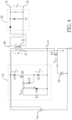
- Fig. 1 shows an example of a circuit configuration of the flyback converter.
- Working principle of the flyback converter is not the focus in the present invention, so is introduced briefly as follows.
- fundamental components of the flyback converter may comprise a transformer 20, a switch Q1, and an output circuit 30.
- a primary-side winding 21 of the transformer 20 is connected to the switch Q1 in series.
- the switch Q1 may be formed by a metal-oxide-semiconductor field-effect transistor (hereinafter referred to as MOSFET), having a gate connected to a pulse width modulation (hereinafter referred to as PWM) controller 40.
- the PWM controller 40 outputs a PWM signal to the switch Q1 to turn on or off the switch Q1.
- a drain of the switch Q1 is connected to the primary-side winding 21.
- the source of the switch Q1 is grounded.
- a terminal of the primary-side 21 of the transformer 20 is connected to an input power Vin, such as a DC (direct current) power as an example herein.
- the output circuit 30 is connected to a secondary-side winding 22 of the transformer 20 and comprises two output terminals 31, 32 to be connected to load(s) .
- the primary-side winding 21 and the secondary-side winding 22 of the transformer 20 are not connected to a same ground.
- the self-driven active clamp circuit 10 of the present invention is connected to the transformer 20 and the switch Q1 and comprises a clamp switch Q2, a first capacitor C1, a second capacitor C2, and a resistor R.
- the self-driven active clamp circuit 10 of the present invention may further comprise a diode D.
- a terminal of the clamp switch Q2 is connected to the first capacitor C1.
- Another terminal of the clamp switch Q2 is connected to the second capacitor C2.
- the clamp switch Q2 is connected between the first capacitor C1 and a second capacitor C2 in series.
- a control terminal of the clamp switch Q2 is connected to the resistor R and the diode D.
- the clamp switch Q2 is formed by a MOSFET.
- a parasitic capacitance C3 exists between a gate and a source of the clamp switch Q2.
- the gate of the clamp switch Q2 is deemed as the above-mentioned control terminal.
- a drain and the source of the clamp switch Q2 are connected to the first capacitor C1 and the second capacitor C2 respectively.
- a terminal of the first capacitor C1 is connected to the primary-side winding 21 of the transformer 20 and the input power Vin. Another terminal of the first capacitor C1 is connected to the drain of the clamp switch Q2.
- a terminal of the second capacitor C2 is connected to the source of the clamp switch Q2. Another terminal of the second capacitor C2 is connected to the drain of the switch Q1 of the flyback converter.
- An anode of the diode D is connected to the gate of the clamp switch Q2.
- a cathode of the diode D is connected to the drain of the switch Q1 of the flyback converter.
- the resistor R is connected to two terminals of the diode D, such that the resistor R is connected across the diode D.
- the vertical axis represents voltage value (V)
- the horizontal axis represents the time.
- Time segment t0 Under the boundary current mode (BCM), the voltage V P on the primary-side winding 21 of the transformer 20 is gradually reduced to 0V.
- the voltage V C2 on the second capacitor C2 is reduced to 0V, too.
- the parasitic capacitance C3 is discharged via the diode D, such that the voltage on the parasitic capacitance C3 is reduced to 0V rapidly.
- the gate voltage of the clamp switch Q2 will be lower than a turn-on threshold voltage (Vgs-th). Then, the clamp switch Q2 is turned off.
- the drain-source voltage V Q1-DS of the switch Q1 is reduced to 0V from a prior high voltage level, and a signal of high is sent to the gate voltage V Q1-G of the switch Q1.
- Control mode of the switch Q1 reaches a zero voltage switching (ZVS).
- Time segment t1 The switch Q1 is turned on. In other words, the switch Q1 changes to on-state from a prior off-state.
- the voltage V P of the primary-side winding 21 rises to Vin from 0V.
- Time segment t2 When gate voltage V Q1-G of the switch Q1 is reduced to a low voltage level (such as the low level in the PWM signal), the switch Q1 changes to the off-state. Because the switch Q1 changes to off-state from a prior on-state, an inverse voltage is generated on the primary-side winding 21 of the transformer 20, so the voltage V P of the primary-side winding 21 shown in Fig. 2H is negative. With reference to Fig. 3 , the voltage V P charges the second capacitor C2 and the first capacitor C1 via a body diode of the clamp switch Q2.
- the second capacitor C2 and the first capacitor C1 also absorb the current spike induced by the leakage inductance of the transformer 20. Then, the second capacitor C2 and the first capacitor C1 will be gradually charged to reach a steady state. Since the body diode is turned on previously, the drain-source voltage V Q2-DS of the clamp switch Q2 is reduced to be lower than approximation of the forward voltage (VF) of the body diode before a driving signal is sent to the clamp switch Q2, as shown in the position "S" of Figs. 2B and 2C . Within the charging duration of the second capacitor C2, as shown in Fig.
- the second capacitor C2 may charge the parasitic capacitance C3 via the resistor R.
- Vgs-th turn-on threshold voltage
- ZVS zero voltage switching
- the gate voltage V Q2-G of the clamp switch Q2 reaches the turn-on threshold voltage (Vgs-th) only when the drain-source voltage V Q2-DS is reduced to approximation of the forward voltage (VF) of the body diode, such that drive and control for the clamp switch Q2 can meet the requirement of the zero voltage switching.
- Time segment t3 Under the boundary current mode (BCM), the voltage V P of the primary-side winding 21 of the transformer 20 will be reduced to 0V gradually.
- the voltage V C2 on the two terminals of the second capacitor C2 is reduced to 0V, too.
- the parasitic capacitance C3 is discharged via the diode D, such that the voltage on the parasitic capacitance C3 is reduced to 0V rapidly.
- the gate voltage of the clamp switch Q2 will be lower than the turn-on threshold voltage (Vgs-th). Then, the clamp switch Q2 is turned off. Because the clamp switch Q2 can be turned off rapidly, the switching loss of the clamp switch Q2 will be decreased.
- the drain-source voltage V Q1-DS of the switch Q1 is gradually reduced to 0V from a prior high voltage level, and the operation within the time segment t0 will be repeated.
- Time segment t4 The switch Q1 is turned on. As shown in Fig. 4 , the operation within the time segment t1 will be repeated.
- the voltage V P is limited by the winding ratio and fails to approximate the ideal driving voltage of 10V due to various demands for input/output.
- the ideal driving voltage approximating 10V will be obtained on the second capacitor C2 according to the voltage division by the first capacitor C1 and the second capacitor C2.
- the gate of the clamp switch Q2 will have a proper driving voltage. Then the present invention will achieve the ideal driving effect.
- the self-driven active clamp circuit of the present invention can autonomously turn on and off the clamp switch Q2 according to the polarity of VP of the primary-side winding 21 without adding further more driving circuits.
- the self-driven active clamp circuit of the present invention not only absorbs the current spike, but also provides the gate of the clamp switch Q2 with the ideal driving voltage by the properly selected second capacitor C2, such that the clamp switch Q2 while turned on may have lower on-state resistance (R DS ), and the loss will be reduced.
Landscapes
- Engineering & Computer Science (AREA)
- Power Engineering (AREA)
- Dc-Dc Converters (AREA)
Abstract
Description
- The present invention relates generally to a self-driven active clamp circuit, and more particularly to an active clamp circuit applied to a flyback converter operating in a boundary current mode (BCM).
- Among various power converters, the flyback converter is very common and may be applied for AC (alternating current)-DC (direct current) conversion or DC-DC conversion. In the flyback converter, because a transformer is applied between input and output of the flyback converter, the flyback converter has advantages of circuit isolation. The flyback converters may be categorized as standard flyback converter and active clamp flyback (ACF) converter.
- For the purposes including absorption of current spikes, energy recycling, and improvement of conversion efficiency, the clamp switch, which is formed by the metal-oxide-semiconductor field-effect transistor (MOSFET), in the primary-side winding of the transformer of the ACF converter replaces the snubber diode of the standard flyback converter.
- The clamp switch is controlled by an individual driving circuit to be turned on and off. Namely, the driving circuit and its power circuit for control are further added to the ACF converter, such that the whole circuit configuration will become much more complicated and detrimental to the reduction in the converter's volume. In addition, while controlling the clamp switch, how to properly drive the clamp switch has to be taken into consideration, such that the conduction loss and the switching loss of the clamp switch will not be too high to have adverse effect on the whole conversion efficiency of the power converter.
- An objective of the present invention is to provide a self-driven active clamp circuit applied to a flyback converter. The present invention can turn on and off a clamp switch without adding further more driving circuits. Besides, the clamp switch while turned on has lower conduction loss and reaches a zero voltage switching (ZVS) itself, such that the switching loss of the clamp loss will be decreased.
- The self-driven active clamp circuit of the present invention is applied to a flyback converter having a transformer and a switch. The self-driven active clamp circuit of the present invention comprises a clamp switch and a resistor. The clamp switch is connected between a first capacitor and a second capacitor in series, wherein another terminal of the first capacitor is connected to a first terminal of a primary-side winding of the transformer, and another terminal of the second capacitor is connected to a second terminal of the primary-side winding of the transformer and the switch of the flyback converter. A terminal of the resistor is connected to a control terminal of the clamp switch. Another terminal of the resistor is connected to the second terminal of the primary-side winding of the transformer and the switch of the flyback converter.
- Preferably, the self-driven active clamp circuit of the present invention further comprises a diode. An anode of the diode is connected to the control terminal of the clamp switch. A cathode of the diode is connected to the second terminal of the primary-side winding of the transformer and the switch of the flyback converter.
- Preferably, the clamp switch is a metal-oxide-semiconductor field-effect transistor (MOSFET) having a gate as the control terminal, a drain connected to the first capacitor, and a source connected to the second capacitor.
- The self-driven active clamp circuit of the present invention can autonomously turn on and off the clamp switch according to the voltage polarity of the primary-side winding of the transformer. The present invention not only absorbs the current spike by the first capacitor and the second capacitor, but also provides the gate of the clamp switch with an ideal driving voltage by a proper selection for the capacitance of the second capacitor. The clamp switch while turned on may have lower on-state resistance (RDS) , such that the loss will be reduced.
-
-
Fig. 1 is a circuit diagram of the self-driven active clamp circuit of the present invention applied to the flyback converter; -
Fig. 2A is a waveform diagram of the output voltage VO as shown inFig. 1 ; -
Fig. 2B is a waveform diagram of the voltage VC2 between two terminals of the second capacitor (C2) as shown inFig. 1 ; -
Fig. 2C is a waveform diagram of the voltage VC1 between two terminals of the first capacitor (C1) as shown inFig. 1 ; -
Fig. 2D is a waveform diagram of the drain-source voltage VQ2-DS of the clamp switch (Q2) as shown inFig. 1 ; -
Fig. 2E is a waveform diagram of the voltage VQ2-G between the gate and the source of the clamp switch (Q2) as shown inFig. 1 ; -
Fig. 2F is a waveform diagram of the drain-source voltage VQ1-DS of the switch (Q1) of the flyback converter as shown inFig. 1 ; -
Fig. 2G is a waveform diagram of the gate voltage VQ1-G of the switch (Q1) of the flyback converter as shown inFig. 1 ; -
Fig. 2H is a waveform diagram of the voltage VP between two terminals of the primary-side winding of the transformer as shown inFig. 1 ; -
Fig. 3 is a circuit diagram of the operation that the switch (Q1) is turned off and the clamp switch (Q2) is turned on; and -
Fig. 4 is a circuit diagram of the operation that the switch (Q1) is turned on and the clamp switch (Q2) is turned off. - The self-driven active clamp circuit of the present invention is connected to a flyback converter.
Fig. 1 shows an example of a circuit configuration of the flyback converter. Working principle of the flyback converter is not the focus in the present invention, so is introduced briefly as follows. - At first, fundamental components of the flyback converter may comprise a
transformer 20, a switch Q1, and anoutput circuit 30. A primary-side winding 21 of thetransformer 20 is connected to the switch Q1 in series. The switch Q1 may be formed by a metal-oxide-semiconductor field-effect transistor (hereinafter referred to as MOSFET), having a gate connected to a pulse width modulation (hereinafter referred to as PWM)controller 40. ThePWM controller 40 outputs a PWM signal to the switch Q1 to turn on or off the switch Q1. A drain of the switch Q1 is connected to the primary-side winding 21. The source of the switch Q1 is grounded. A terminal of the primary-side 21 of thetransformer 20 is connected to an input power Vin, such as a DC (direct current) power as an example herein. - The
output circuit 30 is connected to a secondary-side winding 22 of thetransformer 20 and comprises twooutput terminals transformer 20 are not connected to a same ground. - The self-driven
active clamp circuit 10 of the present invention is connected to thetransformer 20 and the switch Q1 and comprises a clamp switch Q2, a first capacitor C1, a second capacitor C2, and a resistor R. The self-drivenactive clamp circuit 10 of the present invention may further comprise a diode D. A terminal of the clamp switch Q2 is connected to the first capacitor C1. Another terminal of the clamp switch Q2 is connected to the second capacitor C2. Hence, the clamp switch Q2 is connected between the first capacitor C1 and a second capacitor C2 in series. A control terminal of the clamp switch Q2 is connected to the resistor R and the diode D. - In an embodiment of the present invention, the clamp switch Q2 is formed by a MOSFET. A parasitic capacitance C3 exists between a gate and a source of the clamp switch Q2. The gate of the clamp switch Q2 is deemed as the above-mentioned control terminal. A drain and the source of the clamp switch Q2 are connected to the first capacitor C1 and the second capacitor C2 respectively.
- A terminal of the first capacitor C1 is connected to the primary-side winding 21 of the
transformer 20 and the input power Vin. Another terminal of the first capacitor C1 is connected to the drain of the clamp switch Q2. - A terminal of the second capacitor C2 is connected to the source of the clamp switch Q2. Another terminal of the second capacitor C2 is connected to the drain of the switch Q1 of the flyback converter.
- An anode of the diode D is connected to the gate of the clamp switch Q2. A cathode of the diode D is connected to the drain of the switch Q1 of the flyback converter. The resistor R is connected to two terminals of the diode D, such that the resistor R is connected across the diode D.
- With reference to the voltage waveform diagrams shown in
Figs. 2A to 2H , the vertical axis represents voltage value (V), and the horizontal axis represents the time. The circuit operation of the present invention is described as follows. - Time segment t0: Under the boundary current mode (BCM), the voltage VP on the primary-side winding 21 of the
transformer 20 is gradually reduced to 0V. The voltage VC2 on the second capacitor C2 is reduced to 0V, too. The parasitic capacitance C3 is discharged via the diode D, such that the voltage on the parasitic capacitance C3 is reduced to 0V rapidly. As a result, the gate voltage of the clamp switch Q2 will be lower than a turn-on threshold voltage (Vgs-th). Then, the clamp switch Q2 is turned off. At that time, as the voltage reduction of the voltage VP on the primary-side winding 21, the drain-source voltage VQ1-DS of the switch Q1 is reduced to 0V from a prior high voltage level, and a signal of high is sent to the gate voltage VQ1-G of the switch Q1. Control mode of the switch Q1 reaches a zero voltage switching (ZVS). - Time segment t1: The switch Q1 is turned on. In other words, the switch Q1 changes to on-state from a prior off-state. The voltage VP of the primary-side winding 21 rises to Vin from 0V.
- Time segment t2: When gate voltage VQ1-G of the switch Q1 is reduced to a low voltage level (such as the low level in the PWM signal), the switch Q1 changes to the off-state. Because the switch Q1 changes to off-state from a prior on-state, an inverse voltage is generated on the primary-side winding 21 of the
transformer 20, so the voltage VP of the primary-side winding 21 shown inFig. 2H is negative. With reference toFig. 3 , the voltage VP charges the second capacitor C2 and the first capacitor C1 via a body diode of the clamp switch Q2. Within the charging duration of the second capacitor C2 and the first capacitor C1, the second capacitor C2 and the first capacitor C1 also absorb the current spike induced by the leakage inductance of thetransformer 20. Then, the second capacitor C2 and the first capacitor C1 will be gradually charged to reach a steady state. Since the body diode is turned on previously, the drain-source voltage VQ2-DS of the clamp switch Q2 is reduced to be lower than approximation of the forward voltage (VF) of the body diode before a driving signal is sent to the clamp switch Q2, as shown in the position "S" ofFigs. 2B and 2C . Within the charging duration of the second capacitor C2, as shown inFig. 3 , the second capacitor C2 may charge the parasitic capacitance C3 via the resistor R. When the voltage on the parasitic capacitance C3 reaches the turn-on threshold voltage (Vgs-th) of the clamp switch Q2, the clamp switch Q2 changes to on-state to implement the zero voltage switching (ZVS) and absorb the current spike. The resistor R plays a role of a delay component. While charging and based on the delay time determined by the resistor R and the parasitic capacitance C3, the gate voltage VQ2-G of the clamp switch Q2 reaches the turn-on threshold voltage (Vgs-th) only when the drain-source voltage VQ2-DS is reduced to approximation of the forward voltage (VF) of the body diode, such that drive and control for the clamp switch Q2 can meet the requirement of the zero voltage switching. - Time segment t3: Under the boundary current mode (BCM), the voltage VP of the primary-side winding 21 of the
transformer 20 will be reduced to 0V gradually. The voltage VC2 on the two terminals of the second capacitor C2 is reduced to 0V, too. The parasitic capacitance C3 is discharged via the diode D, such that the voltage on the parasitic capacitance C3 is reduced to 0V rapidly. As a result, the gate voltage of the clamp switch Q2 will be lower than the turn-on threshold voltage (Vgs-th). Then, the clamp switch Q2 is turned off. Because the clamp switch Q2 can be turned off rapidly, the switching loss of the clamp switch Q2 will be decreased. The drain-source voltage VQ1-DS of the switch Q1 is gradually reduced to 0V from a prior high voltage level, and the operation within the time segment t0 will be repeated. - Time segment t4: The switch Q1 is turned on. As shown in
Fig. 4 , the operation within the time segment t1 will be repeated. - In a preferred embodiment, in order to minimize the on-state resistance (RDS) and the loss of the clamp switch Q2 while turned on, an ideal driving voltage around 10V as an example should be retained on the gate of the clamp switch Q2. In general, the sum of voltage of the first capacitor C1 and the second capacitor C2, represented as VC1+VC2, is approximately equal to the voltage VP of the primary-side winding 21 while discharging, wherein VP is as the inverse voltage. At that time, the relationship regarding the voltage VP, a winding number NP of the primary-side winding 21, and a winding number NS of the secondary-side winding 22 may be represented as VP= [(NS/NP) ×VO]. In the design practice for the converter, the voltage VP is limited by the winding ratio and fails to approximate the ideal driving voltage of 10V due to various demands for input/output. In the present invention, by selecting a proper capacitance value for the second capacitor C2, the ideal driving voltage approximating 10V will be obtained on the second capacitor C2 according to the voltage division by the first capacitor C1 and the second capacitor C2. The gate of the clamp switch Q2 will have a proper driving voltage. Then the present invention will achieve the ideal driving effect.
- In conclusion, the self-driven active clamp circuit of the present invention can autonomously turn on and off the clamp switch Q2 according to the polarity of VP of the primary-side winding 21 without adding further more driving circuits. The self-driven active clamp circuit of the present invention not only absorbs the current spike, but also provides the gate of the clamp switch Q2 with the ideal driving voltage by the properly selected second capacitor C2, such that the clamp switch Q2 while turned on may have lower on-state resistance (RDS), and the loss will be reduced.
Claims (5)
- A self-driven active clamp circuit (10), characterized in that the self-driven active clamp circuit (10) is connected to a flyback converter having a transformer (20) and a switch (Q1) and comprises:a clamp switch (Q2) connected between a first capacitor (C1) and a second capacitor (C2) in series, wherein another terminal of the first capacitor (C1) is connected to a first terminal of a primary-side winding (21) of the transformer (20), and another terminal of the second capacitor (C2) is connected to a second terminal of the primary-side winding (21) of the transformer (20) and the switch (Q1) of the flyback converter; anda resistor (R), wherein a terminal of the resistor (R) is connected to a control terminal of the clamp switch (Q2), and another terminal of the resistor (R) is connected to the second terminal of the primary-side winding (21) of the transformer (20) and the switch (Q1) of the flyback converter.
- The self-driven active clamp circuit (10) as claimed in claim 1 further comprising a diode (D), wherein an anode of the diode (D) is connected to the control terminal of the clamp switch (Q2), and a cathode of the diode (D) is connected to the second terminal of the primary-side winding (21) of the transformer (20) and the switch (Q1) of the flyback converter.
- The self-driven active clamp circuit (10) as claimed in claim 1 or 2, wherein the clamp switch (Q2) is a metal-oxide-semiconductor field-effect transistor having a gate as the control terminal, a drain connected to the first capacitor (C1), and a source connected to the second capacitor (C2).
- The self-driven active clamp circuit (10) as claimed in claim 3, wherein only when a voltage between the drain and the source of the clamp switch (Q2) is reduced to 0V, a gate voltage of the clamp switch (Q2) rises to turn on the clamp switch (Q2), such that the clamp switch (Q2) operates in zero voltage switching.
- The self-driven active clamp circuit (10) as claimed in claim 4, wherein when the clamp switch (Q2) is turned on, the primary-side winding (21) of the transformer (20) generates an inverse voltage to charge the first capacitor (C1) and the second capacitor (C2).
Priority Applications (1)
| Application Number | Priority Date | Filing Date | Title |
|---|---|---|---|
| EP22161106.4A EP4243262B1 (en) | 2022-03-09 | 2022-03-09 | Self-driven active clamp circuit connected to a flyback converter |
Applications Claiming Priority (1)
| Application Number | Priority Date | Filing Date | Title |
|---|---|---|---|
| EP22161106.4A EP4243262B1 (en) | 2022-03-09 | 2022-03-09 | Self-driven active clamp circuit connected to a flyback converter |
Publications (3)
| Publication Number | Publication Date |
|---|---|
| EP4243262A1 true EP4243262A1 (en) | 2023-09-13 |
| EP4243262A8 EP4243262A8 (en) | 2023-10-18 |
| EP4243262B1 EP4243262B1 (en) | 2026-01-28 |
Family
ID=80684873
Family Applications (1)
| Application Number | Title | Priority Date | Filing Date |
|---|---|---|---|
| EP22161106.4A Active EP4243262B1 (en) | 2022-03-09 | 2022-03-09 | Self-driven active clamp circuit connected to a flyback converter |
Country Status (1)
| Country | Link |
|---|---|
| EP (1) | EP4243262B1 (en) |
Citations (3)
| Publication number | Priority date | Publication date | Assignee | Title |
|---|---|---|---|---|
| US7764515B2 (en) * | 2006-02-14 | 2010-07-27 | Flextronics Ap, Llc | Two terminals quasi resonant tank circuit |
| CN102170232A (en) * | 2011-03-23 | 2011-08-31 | 上海新进半导体制造有限公司 | Self-driven active buffer and flyback switching mode power supply |
| CN107196517B (en) * | 2017-07-04 | 2019-07-19 | 广州金升阳科技有限公司 | The driving circuit of clamp switch in Switching Power Supply |
-
2022
- 2022-03-09 EP EP22161106.4A patent/EP4243262B1/en active Active
Patent Citations (3)
| Publication number | Priority date | Publication date | Assignee | Title |
|---|---|---|---|---|
| US7764515B2 (en) * | 2006-02-14 | 2010-07-27 | Flextronics Ap, Llc | Two terminals quasi resonant tank circuit |
| CN102170232A (en) * | 2011-03-23 | 2011-08-31 | 上海新进半导体制造有限公司 | Self-driven active buffer and flyback switching mode power supply |
| CN107196517B (en) * | 2017-07-04 | 2019-07-19 | 广州金升阳科技有限公司 | The driving circuit of clamp switch in Switching Power Supply |
Also Published As
| Publication number | Publication date |
|---|---|
| EP4243262A8 (en) | 2023-10-18 |
| EP4243262B1 (en) | 2026-01-28 |
Similar Documents
| Publication | Publication Date | Title |
|---|---|---|
| EP1052763B1 (en) | Low loss synchronous rectifier for application to clamped-mode power converters | |
| US7911810B2 (en) | Bi-directional DC-DC converter and method for controlling the same | |
| US5793190A (en) | Method and device for power conversion | |
| US20010024378A1 (en) | Method and arrangement for controlling a synchronous rectifier in a DC/DC converter | |
| EP3509203B1 (en) | Converter with zvs | |
| US6580626B2 (en) | Switching power supply | |
| US8284573B2 (en) | Synchronous rectifier circuit capable of preventing flow-through current | |
| JP5201388B2 (en) | Synchronous rectification drive circuit | |
| US7400519B2 (en) | Switching power supply | |
| US6239989B1 (en) | Forward converter with improved reset circuitry | |
| CN109347311B (en) | Self-driven driving circuit of double-tube forward synchronous rectification circuit | |
| US11990841B2 (en) | Multi-mode hybrid control DC-DC converting circuit and control method thereof | |
| US6430063B1 (en) | Control switch for synchronous rectification circuit of DC-DC converter | |
| JP5040268B2 (en) | Switching power supply | |
| EP4243262B1 (en) | Self-driven active clamp circuit connected to a flyback converter | |
| US11936287B2 (en) | Self-driven active clamp circuit | |
| CN216794868U (en) | Self-excited active clamping circuit | |
| JP7053291B2 (en) | Power converter | |
| US11811299B2 (en) | Direct-current voltage conversion circuit and switching power-supply device | |
| TWI800203B (en) | Self-excited Active Clamp Circuit | |
| KR102142630B1 (en) | Driving circuit of voltage driven synchronous rectifier | |
| EP4243270A1 (en) | Multi-mode hybrid control dc-dc converting circuit and control method thereof | |
| TWM626135U (en) | Self-excited active clamp circuit | |
| JP7825635B2 (en) | Switching control device, switching power supply device and power supply system | |
| JP3169873B2 (en) | Power supply |
Legal Events
| Date | Code | Title | Description |
|---|---|---|---|
| PUAI | Public reference made under article 153(3) epc to a published international application that has entered the european phase |
Free format text: ORIGINAL CODE: 0009012 |
|
| STAA | Information on the status of an ep patent application or granted ep patent |
Free format text: STATUS: REQUEST FOR EXAMINATION WAS MADE |
|
| 17P | Request for examination filed |
Effective date: 20221230 |
|
| AK | Designated contracting states |
Kind code of ref document: A1 Designated state(s): AL AT BE BG CH CY CZ DE DK EE ES FI FR GB GR HR HU IE IS IT LI LT LU LV MC MK MT NL NO PL PT RO RS SE SI SK SM TR |
|
| STAA | Information on the status of an ep patent application or granted ep patent |
Free format text: STATUS: EXAMINATION IS IN PROGRESS |
|
| 17Q | First examination report despatched |
Effective date: 20240911 |
|
| GRAP | Despatch of communication of intention to grant a patent |
Free format text: ORIGINAL CODE: EPIDOSNIGR1 |
|
| STAA | Information on the status of an ep patent application or granted ep patent |
Free format text: STATUS: GRANT OF PATENT IS INTENDED |
|
| INTG | Intention to grant announced |
Effective date: 20251002 |
|
| GRAS | Grant fee paid |
Free format text: ORIGINAL CODE: EPIDOSNIGR3 |
|
| GRAA | (expected) grant |
Free format text: ORIGINAL CODE: 0009210 |
|
| STAA | Information on the status of an ep patent application or granted ep patent |
Free format text: STATUS: THE PATENT HAS BEEN GRANTED |
|
| AK | Designated contracting states |
Kind code of ref document: B1 Designated state(s): AL AT BE BG CH CY CZ DE DK EE ES FI FR GB GR HR HU IE IS IT LI LT LU LV MC MK MT NL NO PL PT RO RS SE SI SK SM TR |
|
| REG | Reference to a national code |
Ref country code: CH Ref legal event code: F10 Free format text: ST27 STATUS EVENT CODE: U-0-0-F10-F00 (AS PROVIDED BY THE NATIONAL OFFICE) Effective date: 20260128 Ref country code: GB Ref legal event code: FG4D |
|
| REG | Reference to a national code |
Ref country code: CH Ref legal event code: R17 Free format text: ST27 STATUS EVENT CODE: U-0-0-R10-R17 (AS PROVIDED BY THE NATIONAL OFFICE) Effective date: 20260202 |
|
| REG | Reference to a national code |
Ref country code: DE Ref legal event code: R096 Ref document number: 602022029051 Country of ref document: DE |
|
| REG | Reference to a national code |
Ref country code: IE Ref legal event code: FG4D |
|
| REG | Reference to a national code |
Ref country code: CH Ref legal event code: U11 Free format text: ST27 STATUS EVENT CODE: U-0-0-U10-U11 (AS PROVIDED BY THE NATIONAL OFFICE) Effective date: 20260401 |
|
| PGFP | Annual fee paid to national office [announced via postgrant information from national office to epo] |
Ref country code: GB Payment date: 20260129 Year of fee payment: 5 |
|
| PGFP | Annual fee paid to national office [announced via postgrant information from national office to epo] |
Ref country code: DE Payment date: 20260121 Year of fee payment: 5 |
|
| PGFP | Annual fee paid to national office [announced via postgrant information from national office to epo] |
Ref country code: AT Payment date: 20260301 Year of fee payment: 5 |
|
| PGFP | Annual fee paid to national office [announced via postgrant information from national office to epo] |
Ref country code: FR Payment date: 20260306 Year of fee payment: 5 |