EP4243245B1 - Verbesserungen der statorwicklung einer leiterplatte für eine axialfeld-rotationsenergievorrichtung - Google Patents
Verbesserungen der statorwicklung einer leiterplatte für eine axialfeld-rotationsenergievorrichtung Download PDFInfo
- Publication number
- EP4243245B1 EP4243245B1 EP23160166.7A EP23160166A EP4243245B1 EP 4243245 B1 EP4243245 B1 EP 4243245B1 EP 23160166 A EP23160166 A EP 23160166A EP 4243245 B1 EP4243245 B1 EP 4243245B1
- Authority
- EP
- European Patent Office
- Prior art keywords
- pcb
- coil
- stator
- layer
- traces
- Prior art date
- Legal status (The legal status is an assumption and is not a legal conclusion. Google has not performed a legal analysis and makes no representation as to the accuracy of the status listed.)
- Active
Links
Images





Classifications
-
- H—ELECTRICITY
- H02—GENERATION; CONVERSION OR DISTRIBUTION OF ELECTRIC POWER
- H02K—DYNAMO-ELECTRIC MACHINES
- H02K1/00—Details of the magnetic circuit
- H02K1/06—Details of the magnetic circuit characterised by the shape, form or construction
- H02K1/12—Stationary parts of the magnetic circuit
-
- H—ELECTRICITY
- H02—GENERATION; CONVERSION OR DISTRIBUTION OF ELECTRIC POWER
- H02K—DYNAMO-ELECTRIC MACHINES
- H02K11/00—Structural association of dynamo-electric machines with electric components or with devices for shielding, monitoring or protection
- H02K11/30—Structural association with control circuits or drive circuits
-
- H—ELECTRICITY
- H02—GENERATION; CONVERSION OR DISTRIBUTION OF ELECTRIC POWER
- H02K—DYNAMO-ELECTRIC MACHINES
- H02K1/00—Details of the magnetic circuit
- H02K1/04—Details of the magnetic circuit characterised by the material used for insulating the magnetic circuit or parts thereof
-
- H—ELECTRICITY
- H02—GENERATION; CONVERSION OR DISTRIBUTION OF ELECTRIC POWER
- H02K—DYNAMO-ELECTRIC MACHINES
- H02K1/00—Details of the magnetic circuit
- H02K1/06—Details of the magnetic circuit characterised by the shape, form or construction
- H02K1/12—Stationary parts of the magnetic circuit
- H02K1/14—Stator cores with salient poles
- H02K1/146—Stator cores with salient poles consisting of a generally annular yoke with salient poles
-
- H—ELECTRICITY
- H02—GENERATION; CONVERSION OR DISTRIBUTION OF ELECTRIC POWER
- H02K—DYNAMO-ELECTRIC MACHINES
- H02K1/00—Details of the magnetic circuit
- H02K1/06—Details of the magnetic circuit characterised by the shape, form or construction
- H02K1/22—Rotating parts of the magnetic circuit
- H02K1/27—Rotor cores with permanent magnets
- H02K1/2793—Rotors axially facing stators
- H02K1/2795—Rotors axially facing stators the rotor consisting of two or more circumferentially positioned magnets
- H02K1/2798—Rotors axially facing stators the rotor consisting of two or more circumferentially positioned magnets where both axial sides of the stator face a rotor
-
- H—ELECTRICITY
- H02—GENERATION; CONVERSION OR DISTRIBUTION OF ELECTRIC POWER
- H02K—DYNAMO-ELECTRIC MACHINES
- H02K21/00—Synchronous motors having permanent magnets; Synchronous generators having permanent magnets
- H02K21/12—Synchronous motors having permanent magnets; Synchronous generators having permanent magnets with stationary armatures and rotating magnets
- H02K21/24—Synchronous motors having permanent magnets; Synchronous generators having permanent magnets with stationary armatures and rotating magnets with magnets axially facing the armatures, e.g. hub-type cycle dynamos
-
- H—ELECTRICITY
- H02—GENERATION; CONVERSION OR DISTRIBUTION OF ELECTRIC POWER
- H02K—DYNAMO-ELECTRIC MACHINES
- H02K3/00—Details of windings
- H02K3/04—Windings characterised by the conductor shape, form or construction, e.g. with bar conductors
- H02K3/26—Windings characterised by the conductor shape, form or construction, e.g. with bar conductors consisting of printed conductors
-
- H—ELECTRICITY
- H02—GENERATION; CONVERSION OR DISTRIBUTION OF ELECTRIC POWER
- H02K—DYNAMO-ELECTRIC MACHINES
- H02K3/00—Details of windings
- H02K3/30—Windings characterised by the insulating material
-
- H—ELECTRICITY
- H02—GENERATION; CONVERSION OR DISTRIBUTION OF ELECTRIC POWER
- H02K—DYNAMO-ELECTRIC MACHINES
- H02K35/00—Generators with reciprocating, oscillating or vibrating coil system, magnet, armature or other part of the magnetic circuit
- H02K35/02—Generators with reciprocating, oscillating or vibrating coil system, magnet, armature or other part of the magnetic circuit with moving magnets and stationary coil systems
-
- H—ELECTRICITY
- H02—GENERATION; CONVERSION OR DISTRIBUTION OF ELECTRIC POWER
- H02K—DYNAMO-ELECTRIC MACHINES
- H02K2203/00—Specific aspects not provided for in the other groups of this subclass relating to the windings
- H02K2203/03—Machines characterised by the wiring boards, i.e. printed circuit boards or similar structures for connecting the winding terminations
-
- H—ELECTRICITY
- H02—GENERATION; CONVERSION OR DISTRIBUTION OF ELECTRIC POWER
- H02K—DYNAMO-ELECTRIC MACHINES
- H02K2211/00—Specific aspects not provided for in the other groups of this subclass relating to measuring or protective devices or electric components
- H02K2211/03—Machines characterised by circuit boards, e.g. pcb
Definitions
- the present disclosure relates in general to an axial field rotary energy device and, in particular, to a system, method and apparatus for motors and generators having one or more printed circuit board (PCB) stators.
- PCB printed circuit board
- PCB printed circuit board
- WO 2021/096804 A1 discloses another example of an axial field electric machine with a printed circuit board stator structure.
- These PCB stator structures are produced through a combination of etching, laminating, drilling and plating operations that can be repeated until a complete PCB stator is obtained. While the manufacturing process of these PCB stators is well established, it is desirable to simplify the manufacturing process to reduce costs.
- Some PCB stator designs require the PCB stator to be split into PCB panels that are processed individually, namely going through etching, laminating, drilling and plating operations, then undergoing additional laminating, drilling, and plating operations. By selecting and applying design features to the PCB stator, some of the previously mentioned repetitive operations can be eliminated resulting in a faster and more economical manufacturing process.
- FIGS. 1-9 disclose various embodiments of axial field rotary energy devices.
- Some axial field electric machines can include one, two or more PCB stators, such as one for each electrical phase of the machine.
- FIGS. 1 and 2 depict a typical multiphase axial field rotary energy device, or multiphase device 100.
- the multiphase device 100 can include at least one rotor 110 (two shown, in FIG. 2 ) with an axis of rotation 120. Each rotor 110 can comprise at least one magnet 130.
- the multiphase device 100 can also include at least one PCB stator 200 that is coaxial with the rotor 110.
- Each PCB stator 200 can include a plurality of coils 210 etched, for example, in the copper foil of a laminated structure of the PCB.
- the coils 210 can be supported by a dielectric structure 215 made of, for example, epoxy-glass laminate, polyimide-glass laminate, or PTFE-ceramic laminate.
- the coils 210 can include multiple turns depending on the design of the PCB stator 200.
- the coils 210 in the PCB stator 200 can be interconnected by means of traces (not shown in FIG. 3A ) etched in the copper foil of a PCB laminate structure to form north and south poles. While FIG. 3A shows an example of a 36-pole stator, many other pole configurations are possible.
- FIG. 3B which is not according to the invention, depicts a coil 210 in more detail.
- Coil 210 can be formed as a continuous conductive trace 211 that can be etched out of a layer of copper foil laminated on a dielectric laminate such as FR4 glass-epoxy laminate, for example.
- the continuous conductive trace 211 of coil 210 can have perforations 212 at both of its terminal ends.
- the perforations 212 can connect coil 210 to other coils in the PCB stator 200.
- coil 210 is shown as having 5-turns, other PCB stators may have coils with different numbers of turns.
- FIG. 3C which is not according to the invention, shows an embodiment where the coils are interconnected to form a continuous path, which is hereinafter referred to as a coil subassembly 220.
- a coil subassembly 220 shows an embodiment where the coils are interconnected to form a continuous path, which is hereinafter referred to as a coil subassembly 220.
- the dielectric material of the PCB laminate structure is not shown for better visualization of the coil structure.
- a first coil 210.1 located on one layer of the PCB structure can have a first terminal 212.1 that can be connected to other coils, or to an external voltage source such as a variable frequency drive (VFD).
- VFD variable frequency drive
- a trace 211.1 can be etched on the copper of a PCB laminate structure to form turns that are terminated at a second terminal 212.2.
- the second terminal 212.2 is coupled to a third terminal 212.3, that is part of a second coil 210.2 located in another layer of the PCB structure, by means of a via, such as a plated via 213.1.
- the second coil 210.2 can have a trace 211.2 that can be etched on the copper of the PCB laminate structure to form turns.
- the trace 211.2 can seamlessly connect and form turns of a third coil 210.3 that terminates at a fourth terminal 212.4.
- the fourth terminal 212.4 can be coupled to a fifth terminal 212.5 that is part of a fourth coil 210.4 located in the same PCB layer as the first coil 210.1.
- the fourth coil 210.4 can have a trace 211.3 that can be etched on the copper of the PCB laminate structure to form turns and terminate at a sixth terminal 212.6.
- the sixth terminal 212.6 can be connected to still other coils, or to an external voltage source such as a VFD.
- coil subassembly 220 is shown as having coils with 5 turns, it should be understood that other coil subassemblies can have different numbers of turns.
- FIGS. 4A and 4B which are not according to the invention, show partial views of an embodiment of the PCB stator 200 where the dielectric material is not shown and the length of the vias is increased for better visualization.
- FIG. 4A shows an example of a 3-phase PCB stator with two layers per phase. Each pair of layers can form a PCB panel that comprises a plurality of coil subassemblies 220.1, 220.2 and 220.3, respectively. Each PCB panel can be assigned to one electrical phase. Each coil subassembly 220.1, 220.2, 220.3 can comprise a set of plated vias 230.1, 230.2 and 230.3, respectively, that connect the coils in each coil subassembly 220.1, 220.2, 220.3 to form a continuous path.
- FIG. 4B shows that the stator panels, and therefore the coil subassemblies, can be rotatably shifted relative to each other by 120 electrical degrees, which is 360 electrical degrees divided by the number of phases.
- 360 electrical degrees cover the angular span of two consecutive poles, or a pair of poles.
- the PCB stator example shown in FIGS. 3A-4B has 36 poles.
- each pole in this one example has a physical span of 10 mechanical (or electrical) degrees and a pair of poles has a physical span of 20 mechanical (or electrical) degrees.
- 360 electrical degrees are equivalent to 20 mechanical degrees and 120 electrical degrees are equivalent to 6.67 mechanical degrees.
- FIGS. 4A and 4B show a 3-phase stator structure
- PCB stators can have 2, 4, 5, 6, or another number of phases. It should also be noted that although each phase in PCB stator 200 has one pair of layers per phase, other PCB stators can have 2, 3, 4 or more pairs of layers per phase.
- FIG. 4B shows a top view of the PCB stator 200 where the locations of vias 230.1, 230.2 and 230.3 are indicated.
- vias 230.1 which are in coil subassembly 220.1
- vias 230.2 which are in coil subassembly 220.2
- vias 230.3 of coil subassembly 220.3 are substantially vertically aligned with traces 232 from other layers.
- FIG. 5 shows a flow diagram of an embodiment of a manufacturing process 300 for a PCB stator which is not according to the invention, were vias could intersect traces as depicted in the example in FIGS. 4A and 4B .
- each PCB panel can undergo the process 301 that can include application of a photoresist, etching, resist stripping, panel lamination, via drilling and via plating.
- the process can be repeated for each phase of the PCB panel.
- the phases panels of the PCB stators can undergo process 302, where they are laminated together to form the complete PCB stator. Subsequently, they can be drilled, plated, coated with resist, etched, stripped of remaining resist and coated with a solder mask, for example.
- FIG. 5 describes a process for a stator with three PCB panels with one panel per electrical phase
- other PCB stators can have 2, 4, 5, 6 or more PCB panels with one panel per phase, so the process 301 can match the number of panels and/or phases.
- the reason that the vias 230.1, 230.2, 230.3 can intersect the other coil traces is because the number of coil turns is not a multiple of the number of phases.
- the example in FIGS. 4A and 4B has coils with 5 turns which is not a multiple of 3, which is the number of phases.
- FIGS. 6A and 6B show an example of a 3-phase PCB stator 400 that have coils with 6 turns, which is multiple of 3, which is the number of phases in PCB stator 400.
- the dielectric material is not shown and the length of the vias are increased for easier visualization.
- the 3-phase PCB stator 400 has 2 layers per phase. Each pair of layers can form a PCB panel that comprises a plurality of coil subassemblies 420.1, 420.2 and 420.3, respectively, and each PCB panel can be assigned to one electrical phase.
- Each coil subassembly can comprise a set of plated vias 430.1, 430.2 and 430.3, respectively, that connects the coils in each coil subassembly 420.1, 420.2, 420.3 to form a continuous path.
- the PCB stator panels in FIGS. 6A and 6B are rotatably shifted relative to each other by 120 electrical degrees, which is 360 electrical degrees divided by the number of phases. It should be noted that although each phase in PCB stator 400 has one pair of layers, other PCB stators can have 2, 3, 4 or more pairs of layers per phase.
- via 430.1 in coil subassembly 420.1 can be extended along the line 431.1, which is substantially co-linear with via 430.1, without intersecting any traces 432 in any other layers.
- via 430.2 in coil subassembly 420.2 can be extended along the line 431.2, which is substantially co-linear with via 430.2, without intersecting any traces 432 in any other layers.
- via 430.3 in coil subassembly 420.3 can be extended along the line 431.3, which is substantially co-linear with via 430.3 without intersecting any traces 432 in any other layers.
- FIG. 6B shows a top view of PCB stator 400 where the vias 430.1, 430.2 and 430.3 are indicated. It can be seen that the vias 430.1, 430.2, 430.3 do not intersect any traces 432 other than the traces in the layers that form the coils they are coupled to. In this embodiment where the number of turns of the coils is a multiple of the number of electrical phases, a via and its extension will intersect traces only in coils that belong to layers associated to that one phase. Said via and its extension will not intersect traces in coils that belong to layers associated with the other phases.
- FIGS. 6A and 6B allow for a PCB manufacturing process 500 depicted in FIG. 7 , which has fewer steps than the manufacturing process 300 depicted in FIG. 5 . This is because all PCB stator layers can be laminated, via drilled and plated in one single step, which is faster and more economical than the manufacturing process 300 depicted in FIG. 5 .
- the PCB stator can have coils connected in series, parallel, or a combination of both.
- each coil of the PCB stator has two or more parallel traces.
- the current flowing through the coils of the PCB stator can be split among parallel traces.
- the traces do not intersect each other along the coils, because that would create paths for eddy current circulation, which would create eddy current losses and degrade machine efficiency.
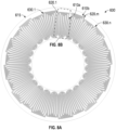
- FIG. 8A shows an example of a PCB stator 600 according to the invention with parallel traces that can include a plurality of coils 610, 620.1 through 620.m, and coils 630.1 through 630.n.
- the coils may be etched, for example, in the copper foil of a laminated structure of the PCB. These copper coils can be supported by a dielectric structure 615 formed from, for example, epoxy-glass laminate, polyimide-glass laminate, or PTFE-ceramic laminate.
- the coils 610, 620.1 through 620.m, and 630.1 through 630.n can include multiple turns depending on the design of the PCB stator. While FIG. 8A shows an example of a 24-pole stator, many other pole configurations are possible.
- the PCB stator example shown in FIG. 8A has three turns per coil, however, other PCB stators can have coils with other numbers of turns.
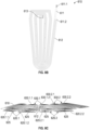
- FIG. 8B shows an embodiment of an individual coil 610 which can have a terminal 611 that can be connected to an external voltage source, such as a VFD, at a first end 611.1. At a second end 611.2, the terminal 611 can be split into multiple parallel traces 612 that form the coil 610.
- FIG. 8B shows the coil 610 with three parallel traces 612, other embodiments can have coils with two, four, five or more parallel traces.
- Each trace 612 in coil 610 terminates in a respective terminal 613 ( FIG. 8B ).
- the terminals 613 are not connected to each other in any of the coils 610a, 620.1 through 620.m, or 630.1 to 630.n, until they circumscribe (in a counterclockwise direction, in FIG. 8A ) the entire PCB stator 600.
- the only point where the traces 612 reconnect is the second end 611.2 of terminal 611 of the second coil 610b (on the right side of FIG. 8A ).
- the current from the external source can enter at coil 610a (via terminal 611), split into traces 612 and then exit at the terminal 611 of coil 610b.
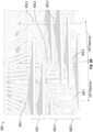
- FIG. 8C shows a detailed view of an embodiment of a PCB stator where the dielectric structure is not shown for ease of understanding.
- the coil 610 can be in one layer and connected to a coil 620.1 in another layer with vias 625.
- Coil 620.1 can have a first part 620.1.1 that can be circumferentially aligned with coil 610.
- a second part 620.1.2 can be in the same layer and adjacent to the first part 620.1.1 to form a continuous path of three non-intersecting traces.
- the second part 620.1.2 can be connected (with vias 625) to a first part 630.1.1 of a coil 630.1 that is in the same layer as coil 610.
- Second part 620.1.2 and first part 630.1.1 can be circumferentially aligned.
- the second part 630.1.2 of coil 630.1 can be connected with vias 625 to a first part 620.2.1 of a coil 620.2 that is located in the same layer as the coil 620.1.
- Coils 620.1 and 620.2 can be identical to each other.
- Second part 630.1.2 and 620.2.1 can be circumferentially aligned.
- the second part 620.2.2 of the coil 620.2 can be connected to the first part 630.2.1 of a coil 630.2 that is located in the same layer as the coil 630.1 and coil 610.
- Coils 6301. And 630.2 can be identical to each other.
- Coils 620.2.2 and 630.2.1 can be circumferentially aligned.
- This pattern can repeat for the entire circumference of the PCB stator for up to coils 620.m and 630.n.
- the second part 620.m.2 of the last coil 620.m can connect to another coil 610 (which can be identical to the original coil 610), as shown in FIG. 8A .
- the traces 612 ( FIGS. 8B and 8C ) only intersect each other at the terminals 611 at both ends of the PCB stator panel winding.
- a continuous serial path is formed through the vias connections that each trace in each coil forms with corresponding traces in other coils.
- Embodiments of the PCB stator 600 can have coils where the number of turns is a multiple of the number of phases.
- FIG. 9A depicts a partial view of the PCB stator 600 having three panels 600.1, 600.2 and 600.3, and each panel is assigned to one phase.
- panels 600.1, 600.2 and 600.3 have one pair of layers each, however other embodiments can have more than one pair of layers.
- FIG. 9B shows a detailed view of a portion of the PCB stator 600 where the dielectric structure is not shown for ease of understanding.
- PCB Stator 600 is 3-phase stator and has coils with 3 turns.
- the via extensions 635.1, 635.2 and 635.3 can extend from the vias 625.1, 625.2 and 625.3, respectively, and intersect only the traces associated with the respective phases.
- FIG. 10 is an enlarged cross-sectional view of a portion of a PCB stator showing a via and PCB layer details.
- FIG. 11 is a process flow chart for manufacturing an embodiment of a PCB stator.
- FIG. 12A is an enlarged view of a surface detail of a PCB stator.
- FIG. 12B is a further enlarged view of the detail shown in FIG. 12A .
- FIG.10 shows a partial cross section of a PCB stator 700.
- PCB stator 700 includes a via 710 that can extend from one major surface (e.g., flat surface, in some examples) of the PCB stator 700 to another major surface thereof.
- the via 710 can be plated (see, e.g., step 805 in the manufacturing process 800 shown in FIG. 11 ) with a material having high thermal conductivity, such as copper, for example.
- the vias 710 can include one or more substantially cylindrical, electrically conductive tubes 715 that extend from one major surface of the PCB stator to the opposing major surface.
- the conductive tubes 715 are alternatively depicted as vias 625.2 and 635.2 in FIG. 9B , for example. As shown in FIG. 10 , the tube 715 can be electrically connected to selected ones of the traces 701 while selectively not intersecting other traces 702 in the PCB stator 700.
- a conductive pad 716 can be formed on the outer surface of the PCB stator 700.
- a voltage of hundreds of volts can be applied to the pad 716, in some examples.
- layers of B-stage glass-epoxy laminate for example, can be laminated onto the external major surfaces of the PCB stator 700.
- the laminate can form a dielectric layer 720 that can completely cover and isolate the pad 716 electrically from surrounding components, such as rotor 110.
- the lamination of the dielectric layer 720 is represented by step 806 ( FIG. 11 ) in the PCB stator manufacturing process 800.
- This process can be simpler and more economical than the manufacturing processes 300 and 500 ( FIGS. 5 and 7 , respectively) where a solder mask coat is applied to the surfaces of the PCB stator.
- the dielectric layer 720 can have a high dielectric strength, such as 40 kV/mm, for example, and can enable the PCB stator 700 to withstand up to 3,000 Vdc or more during high voltage testing in some embodiments. This represents a substantial improvement over a typical solder mask coat which is not intended to provide dielectric protection and cannot withstand more than 1,000 Vdc in a high voltage test, for example.
- Embodiments of the PCB stator manufacturing process 800 can include other steps such as a resist coat lamination 801, an etch and strip resist 802, stator lamination 803 and stator drilling 804.
- Some embodiments can have a laminated dielectric layer 720 made of a B-stage glass epoxy laminate, with typical off-plane thermal conductivity of 0.2 to 0.3 W/m.K.
- Other embodiments can employ a B-stage glass epoxy laminate with high off-plane thermal conductivity in the 2 to 3 W/m.K range.
- some embodiments can employ glass reinforced laminates with other resins, such as polyimide or polytetrafluorethylene based resins or others.
- the dielectric layer 720 can be configured to conform to features on the surface of the PCB stator 700.
- FIG. 12A shows an example of an embodiment of the dielectric layer 720 with a cutout 721 forming a recess providing clearance around conductive pads 730.
- the conductive pads 730 can receive, by means of soldering, an resistance temperature detector (RTD), for example, to sense the temperature of the PCB stator 700 during operation.
- RTD resistance temperature detector
- the conductive pads 730 can be configured to receive other sensors 733 (shown schematically in FIG. 12B ) such as thermistors, accelerometers, or other sensing devices.
- the conductive pads 730 can be connected to terminals 731 ( FIG. 12B ) by means of conductive traces 732.
- the conductive pads 730, terminals 731 and conductive traces 732 can be made from copper or other metal or alloy with good electrical conductivity and can be formed by etching.
- a masking pattern 740 can be applied to the surface of the PCB stator 700.
- the masking pattern 740 can be applied with a silk-screen printing or ink jet printing, for example. Such processing can eliminate the need to apply a solder mask, which is a more complicated and expensive process.
- the masking pattern 740 can be configured to cover the conductive traces 732 that connect the conductive pads 730 to terminals 731 to protect conductive traces 732 from oxidation.
- the masking pattern 740 can comprise an extension 741 that provides a barrier to prevent molten solder from bridging the gap between the adjacent conductive pads 730 during the soldering operation.
- the masking pattern 740 can further comprise a contour 742 for preventing molten solder from running off over the surface of the PCB stator 700.
- the masking pattern 740 can be 25 ⁇ m thick, for example, however other thicknesses can also be employed.
- an axial field rotary energy device comprising:
- the device comprising one or more of: each end of the plated vias comprises plated pads; the dielectric layer has an off-plane thermal conductivity that is greater than 2 W/m.K; or the dielectric layer has a dielectric strength of 40 kV/mm or more.
- the device further comprising one or more of:
- the device further comprising one or more of: the masking pattern is at least 25 ⁇ m thick; the plated vias have plated pads at each end; the dielectric layer has an off-plane thermal conductivity that is greater than 2 W/m.K; or the dielectric layer has a dielectric strength of 40 kV/mm or more.
- the device further comprising:
- the plated vias have plated pads at each end.
- the layer of dielectric material has an off-plane thermal conductivity that is greater than 2 W/m.K.
- the layer of dielectric material has a dielectric strength of 40 kV/mm or more.
- the device further comprising conductive pads coupled to sensors, and the conductive pads are connected to terminals through conductive traces.
- the conductive pads, terminals and conductive traces are comprised of an electrically conductive material.
- the dielectric layer on at least one of the major surfaces of the PCB stator has cut outs that provide clearance around the conductive pads.
- the device further comprising a masking pattern that covers conductive traces and forms barriers to prevent molten solder from bridging across adjacent ones of conductive pads and from running off on the major surfaces of the PCB stator.
- each major surface of the PCB stator is laminated with the dielectric material layer.
- an axial field rotary energy device comprising:
- the layer of dielectric material has an off-plane thermal conductivity that is greater than 2 W/m.K.
- the device further comprising:
- the masking pattern is at least 25 ⁇ m thick.
- the layer of dielectric material has an off-plane thermal conductivity that is greater than 2 W/m.K.
- first, second, third, etc. may be used herein to describe various elements, components, regions, layers and/or sections, these elements, components, regions, layers and/or sections should not be limited by these terms. These terms may be only used to distinguish one element, component, region, layer or section from another region, layer or section. Terms such as “first,” “second,” and other numerical terms when used herein do not imply a sequence or order unless clearly indicated by the context. Thus, a first element, component, region, layer or section discussed below could be termed a second element, component, region, layer or section without departing from the teachings of the example embodiments.
- spatially relative terms such as “inner,” “outer,” “beneath,” “below,” “lower,” “above,” “upper,” “top”, “bottom,” and the like, may be used herein for ease of description to describe one element's or feature's relationship to another element(s) or feature(s) as illustrated in the figures.
- Spatially relative terms may be intended to encompass different orientations of the device in use or operation in addition to the orientation depicted in the figures. For example, if the device in the figures is turned over, elements described as “below” or “beneath” other elements or features would then be oriented “above” the other elements or features.
- the example term “below” can encompass both an orientation of above and below.
- the device may be otherwise oriented (rotated degrees or at other orientations) and the spatially relative descriptions used herein interpreted accordingly.
- the term “or” is inclusive, meaning and/or.
- phrases "at least one of,” when used with a list of items, means that different combinations of one or more of the listed items can be used, and only one item in the list can be needed.
- “at least one of: A, B, and C” includes any of the following combinations: A, B, C, A and B, A and C, B and C, and A and B and C.
Landscapes
- Engineering & Computer Science (AREA)
- Power Engineering (AREA)
- Windings For Motors And Generators (AREA)
Claims (13)
- Eine Axialfeld-Rotationsenergievorrichtung (100), umfassend:einen Rotor (110), der eine Drehachse und einen Magneten umfasst;einen zum Rotor koaxialen Stator (400, 600), wobei der Stator Leiterplatten(PCB)-felder umfasst, jedes PCB-Feld ist einer elektrischen Phase der Vorrichtung zugeordnet, jedes PCB-Feld umfasst mindestens ein Paar PCB-Lagen und jede PCB-Lage umfasst Spulen;dadurch gekennzeichnet, dassjede Spule in jeder PCB-Lage eines gegebenen PCB-Feldes in Umfangsrichtung mit einer entsprechenden Spule in einer anderen PCB-Lage des gegebenen PCB-Feldes ausgerichtet ist;wobeieine Spule in einer PCB-Lage mit einer entsprechenden Spule in einer anderen PCB-Lage des gegebenen PCB-Feldes mit einem jeweiligen Durchgang (430, 625) gekoppelt ist; undeine Anzahl von Windungen in jeder Spule ein Vielfaches einer Anzahl von elektrischen Phasen ist, die für die Vorrichtung konfiguriert sind, so dass die Durchgänge (430) und ihre Verlängerungen keine Bahnen (432) von Spulen schneiden, die zu PCB-Lagen gehören, die anderen Phasen zugeordnet sind,
oderjede Spule in jeder PCB-Lage des gegebenen PCB-Feldes in Umfangsrichtung mit einer entsprechenden Spule in einer anderen PCB-Lage des gegebenen PCB-Feldes ausgerichtet und gekoppelt ist; undjede Spule Bahnen (612) umfasst, die nicht miteinander verbunden sind, außer an Anschlüssen (611) einer ersten Spule und einer letzten Spule der gekoppelten Spulen eines jeweiligen des Paars von PCB-Lagen. - Die Vorrichtung nach Anspruch 1, wobei jede Spule Bahnen (612) umfasst, die parallel zueinander sind, und/oder die Bahnen (612) in jeder Spule nicht miteinander verbunden sind, außer an den Anschlüssen (611) einer ersten Spule und einer letzten Spule eines jeweiligen des Paares von PCB-Lagen.
- Die Vorrichtung nach Anspruch 2, wobei der Stator für drei elektrische Phasen eingerichtet ist, und die Anzahl der Windungen in den Spulen ein Vielfaches von drei ist.
- Die Vorrichtung nach einem der vorhergehenden Ansprüche, wobei jedes PCB-Feld eine Vielzahl von leitenden Lagen umfassend, und ausgewählte der leitenden Lagen mit plattierten Durchgängen (710) verbunden sind, die sich von einer Hauptfläche des PCB-Stators zu einer gegenüberliegenden Hauptfläche des PCB-Stators erstrecken; und
jede Hauptfläche des PCB-Stators eine Lage (720) aus einem dielektrischen Material umfasst, die Enden der plattierten Durchgänge vollständig bedeckt. - Die Vorrichtung nach dem vorhergehenden Anspruch, wobei die Lage des dielektrischen Materials eine Durchschlagfestigkeit von 40 kV/mm oder mehr aufweist.
- Die Vorrichtung nach einem der beiden vorhergehenden Ansprüche, wobei die Lage des dielektrischen Materials eine Wärmeleitfähigkeit außerhalb der Ebene aufweist, die größer als 2 W/m.K ist.
- Die Vorrichtung nach einem der drei vorhergehenden Ansprüche, ferner umfassend eines oder mehrere von:leitenden Pads (730), die mit Sensoren gekoppelt sind, und die leitenden Pads sind über Leiterbahnen mit Anschlüssen verbunden;die leitenden Pads, Anschlüsse und Leiterbahnen umfassen ein elektrisch leitendes Material.
- Die Vorrichtung nach dem vorhergehenden Anspruch, wobeidie dielektrische Lage auf mindestens einer der Hauptflächen des PCB-Stators Aussparungen aufweist, die einen Freiraum um die leitenden Pads bereitstellen;
und/oderein Maskierungsmuster die Leiterbahnen bedeckt und Barrieren bildet, um zu verhindern, dass geschmolzenes Lot Benachbarte der leitenden Pads überbrückt und auf die Hauptflächen des PCB-Stators abfließt. - Die Vorrichtung nach dem vorhergehenden Anspruch, wobei das Maskierungsmuster mindestens 25 µm dick ist.
- Die Vorrichtung nach einem der vorhergehenden Ansprüche, wobei sich der Durchgang von einer Hauptfläche des PCB-Stators zu einer gegenüberliegenden Hauptfläche des PCB-Stators erstreckt.
- Die Vorrichtung nach einem der vorhergehenden Ansprüche, wobei jedes Ende der plattierten Durchgänge plattierte Pads umfasst.
- Die Vorrichtung nach Anspruch 4 oder einem der vorhergehenden acht Ansprüche, wobei jede Hauptfläche des PCB-Stators mit der Lage des dielektrischen Materials laminiert ist.
- Die Vorrichtung nach Anspruch 4 oder einer der vorhergehenden neun Ansprüche, wobei die Lage des dielektrischen Materials die Enden der plattierten Durchgänge und/oder die jeweiligen Pads vollständig bedeckt.
Priority Applications (1)
| Application Number | Priority Date | Filing Date | Title |
|---|---|---|---|
| EP24195310.8A EP4439936A3 (de) | 2022-03-07 | 2023-03-06 | Verbesserungen der statorwicklung einer leiterplatte für eine axialfeld-rotationsenergievorrichtung |
Applications Claiming Priority (3)
| Application Number | Priority Date | Filing Date | Title |
|---|---|---|---|
| US17/688,451 US11502583B1 (en) | 2022-03-07 | 2022-03-07 | Printed circuit board stator winding enhancements for axial field rotary energy device |
| US17/880,817 US11616423B1 (en) | 2022-03-07 | 2022-08-04 | Printed circuit board stator winding enhancements for axial field rotary energy device |
| US17/945,403 US11750071B1 (en) | 2022-03-07 | 2022-09-15 | Printed circuit board stator winding enhancements for axial field rotary energy device |
Related Child Applications (1)
| Application Number | Title | Priority Date | Filing Date |
|---|---|---|---|
| EP24195310.8A Division EP4439936A3 (de) | 2022-03-07 | 2023-03-06 | Verbesserungen der statorwicklung einer leiterplatte für eine axialfeld-rotationsenergievorrichtung |
Publications (3)
| Publication Number | Publication Date |
|---|---|
| EP4243245A1 EP4243245A1 (de) | 2023-09-13 |
| EP4243245B1 true EP4243245B1 (de) | 2024-09-11 |
| EP4243245C0 EP4243245C0 (de) | 2024-09-11 |
Family
ID=85505689
Family Applications (2)
| Application Number | Title | Priority Date | Filing Date |
|---|---|---|---|
| EP23160166.7A Active EP4243245B1 (de) | 2022-03-07 | 2023-03-06 | Verbesserungen der statorwicklung einer leiterplatte für eine axialfeld-rotationsenergievorrichtung |
| EP24195310.8A Pending EP4439936A3 (de) | 2022-03-07 | 2023-03-06 | Verbesserungen der statorwicklung einer leiterplatte für eine axialfeld-rotationsenergievorrichtung |
Family Applications After (1)
| Application Number | Title | Priority Date | Filing Date |
|---|---|---|---|
| EP24195310.8A Pending EP4439936A3 (de) | 2022-03-07 | 2023-03-06 | Verbesserungen der statorwicklung einer leiterplatte für eine axialfeld-rotationsenergievorrichtung |
Country Status (5)
| Country | Link |
|---|---|
| US (1) | US11750071B1 (de) |
| EP (2) | EP4243245B1 (de) |
| CA (1) | CA3190044A1 (de) |
| IE (1) | IES87425Y1 (de) |
| MX (1) | MX2023002703A (de) |
Families Citing this family (3)
| Publication number | Priority date | Publication date | Assignee | Title |
|---|---|---|---|---|
| US12621930B2 (en) * | 2023-03-28 | 2026-05-05 | Infinitum Electric Inc. | Printed circuit board dielectric molding or machining and electrolytic metallization |
| EP4554058A1 (de) * | 2023-11-09 | 2025-05-14 | Airbus S.A.S. | Statorsystem für eine axialflussmaschine für ein flugzeug sowie antriebsstrang und flugzeug damit |
| WO2025217730A1 (en) * | 2024-04-15 | 2025-10-23 | Litens Automotive Partnership | Torque efficient axial flux printed circuit board stator |
Family Cites Families (12)
| Publication number | Priority date | Publication date | Assignee | Title |
|---|---|---|---|---|
| US7109625B1 (en) * | 2003-02-07 | 2006-09-19 | Jore Lincoln M | Conductor optimized axial field rotary energy device |
| EP3128646A1 (de) | 2009-01-16 | 2017-02-08 | Boulder Wind Power, Inc. | Segmentierter stator für eine axiale feldvorrichtung |
| EP2671306B1 (de) * | 2011-01-31 | 2015-08-05 | Hitachi Koki Co., Ltd. | Scheibenmotor, elektrische arbeitsmaschine mit dem scheibenmotor und verfahren zur herstellung des scheibenmotors |
| FR2994038B1 (fr) * | 2012-07-27 | 2017-04-28 | David Libault | Moteur electrique a flux axial |
| US8736133B1 (en) | 2013-03-14 | 2014-05-27 | Boulder Wind Power, Inc. | Methods and apparatus for overlapping windings |
| US20150155070A1 (en) * | 2013-12-04 | 2015-06-04 | General Electric Company | Insulation for electrical components |
| US9793775B2 (en) * | 2013-12-31 | 2017-10-17 | Boulder Wind Power, Inc. | Methods and apparatus for reducing machine winding circulating current losses |
| US10170953B2 (en) * | 2015-10-02 | 2019-01-01 | E-Circuit Motors, Inc. | Planar composite structures and assemblies for axial flux motors and generators |
| US10135310B2 (en) | 2017-01-11 | 2018-11-20 | Infinitum Electric Inc. | System and apparatus for modular axial field rotary energy device |
| US10186922B2 (en) | 2017-01-11 | 2019-01-22 | Infinitum Electric Inc. | System and apparatus for axial field rotary energy device |
| US20210203213A1 (en) * | 2017-11-06 | 2021-07-01 | Core Innovation, Llc | Structures and methods of manufacture of serpentine stator coils |
| US11283319B2 (en) * | 2019-11-11 | 2022-03-22 | Infinitum Electric, Inc. | Axial field rotary energy device with PCB stator having interleaved PCBS |
-
2022
- 2022-09-15 US US17/945,403 patent/US11750071B1/en active Active
-
2023
- 2023-02-16 CA CA3190044A patent/CA3190044A1/en active Pending
- 2023-03-03 MX MX2023002703A patent/MX2023002703A/es unknown
- 2023-03-06 EP EP23160166.7A patent/EP4243245B1/de active Active
- 2023-03-06 EP EP24195310.8A patent/EP4439936A3/de active Pending
- 2023-03-06 IE IE20230048U patent/IES87425Y1/en unknown
Also Published As
| Publication number | Publication date |
|---|---|
| EP4439936A2 (de) | 2024-10-02 |
| IE20230048U1 (en) | 2023-09-13 |
| CA3190044A1 (en) | 2023-09-07 |
| US11750071B1 (en) | 2023-09-05 |
| MX2023002703A (es) | 2023-09-08 |
| EP4243245A1 (de) | 2023-09-13 |
| IES87425Y1 (en) | 2023-09-13 |
| EP4439936A3 (de) | 2025-01-08 |
| EP4243245C0 (de) | 2024-09-11 |
| US20230283152A1 (en) | 2023-09-07 |
Similar Documents
| Publication | Publication Date | Title |
|---|---|---|
| EP4439936A2 (de) | Verbesserungen der statorwicklung einer leiterplatte für eine axialfeld-rotationsenergievorrichtung | |
| US11502583B1 (en) | Printed circuit board stator winding enhancements for axial field rotary energy device | |
| US8785784B1 (en) | Methods and apparatus for optimizing structural layout of multi-circuit laminated composite assembly | |
| US8736133B1 (en) | Methods and apparatus for overlapping windings | |
| US10170953B2 (en) | Planar composite structures and assemblies for axial flux motors and generators | |
| EP2566012B1 (de) | Motorstator | |
| EP2382701B1 (de) | Segmentierter stator für eine axiale feldvorrichtung | |
| US10355550B2 (en) | Methods and apparatus for reducing machine winding circulating current losses | |
| EP1168574B1 (de) | Elektrische Maschine | |
| KR100755556B1 (ko) | 도체 최적화된 축 방향 필드 회전 에너지 장치 | |
| US8723052B1 (en) | Methods and apparatus for optimizing electrical interconnects on laminated composite assemblies | |
| CN110138121B (zh) | 蛇形定子线圈结构及制造方法 | |
| US11605993B2 (en) | Rotary motors incorporating flexible printed circuit boards | |
| US20250219489A1 (en) | Printed circuit board stator winding enhancements for axial field rotary energy device | |
| WO2005050818A1 (en) | Electric machine improvement | |
| US12603558B2 (en) | Printed circuit board stator winding enhancements for axial field rotary energy device | |
| US10225934B2 (en) | Magnetic circuit board and method for manufacturing same | |
| JP2020527014A5 (de) | ||
| JP4157319B2 (ja) | 結線基板 | |
| WO2025248809A1 (ja) | 電機子、回転電機、及び電機子の製造方法 | |
| WO2025248808A1 (ja) | 電機子及び回転電機 |
Legal Events
| Date | Code | Title | Description |
|---|---|---|---|
| PUAI | Public reference made under article 153(3) epc to a published international application that has entered the european phase |
Free format text: ORIGINAL CODE: 0009012 |
|
| STAA | Information on the status of an ep patent application or granted ep patent |
Free format text: STATUS: THE APPLICATION HAS BEEN PUBLISHED |
|
| AK | Designated contracting states |
Kind code of ref document: A1 Designated state(s): AL AT BE BG CH CY CZ DE DK EE ES FI FR GB GR HR HU IE IS IT LI LT LU LV MC ME MK MT NL NO PL PT RO RS SE SI SK SM TR |
|
| STAA | Information on the status of an ep patent application or granted ep patent |
Free format text: STATUS: REQUEST FOR EXAMINATION WAS MADE |
|
| 17P | Request for examination filed |
Effective date: 20240214 |
|
| RBV | Designated contracting states (corrected) |
Designated state(s): AL AT BE BG CH CY CZ DE DK EE ES FI FR GB GR HR HU IE IS IT LI LT LU LV MC ME MK MT NL NO PL PT RO RS SE SI SK SM TR |
|
| GRAP | Despatch of communication of intention to grant a patent |
Free format text: ORIGINAL CODE: EPIDOSNIGR1 |
|
| STAA | Information on the status of an ep patent application or granted ep patent |
Free format text: STATUS: GRANT OF PATENT IS INTENDED |
|
| INTG | Intention to grant announced |
Effective date: 20240412 |
|
| GRAS | Grant fee paid |
Free format text: ORIGINAL CODE: EPIDOSNIGR3 |
|
| GRAA | (expected) grant |
Free format text: ORIGINAL CODE: 0009210 |
|
| STAA | Information on the status of an ep patent application or granted ep patent |
Free format text: STATUS: THE PATENT HAS BEEN GRANTED |
|
| AK | Designated contracting states |
Kind code of ref document: B1 Designated state(s): AL AT BE BG CH CY CZ DE DK EE ES FI FR GB GR HR HU IE IS IT LI LT LU LV MC ME MK MT NL NO PL PT RO RS SE SI SK SM TR |
|
| REG | Reference to a national code |
Ref country code: GB Ref legal event code: FG4D |
|
| REG | Reference to a national code |
Ref country code: CH Ref legal event code: EP |
|
| REG | Reference to a national code |
Ref country code: DE Ref legal event code: R096 Ref document number: 602023000524 Country of ref document: DE |
|
| REG | Reference to a national code |
Ref country code: IE Ref legal event code: FG4D |
|
| U01 | Request for unitary effect filed |
Effective date: 20241007 |
|
| U07 | Unitary effect registered |
Designated state(s): AT BE BG DE DK EE FI FR IT LT LU LV MT NL PT RO SE SI Effective date: 20241028 |
|
| PG25 | Lapsed in a contracting state [announced via postgrant information from national office to epo] |
Ref country code: NO Free format text: LAPSE BECAUSE OF FAILURE TO SUBMIT A TRANSLATION OF THE DESCRIPTION OR TO PAY THE FEE WITHIN THE PRESCRIBED TIME-LIMIT Effective date: 20241211 |
|
| PG25 | Lapsed in a contracting state [announced via postgrant information from national office to epo] |
Ref country code: GR Free format text: LAPSE BECAUSE OF FAILURE TO SUBMIT A TRANSLATION OF THE DESCRIPTION OR TO PAY THE FEE WITHIN THE PRESCRIBED TIME-LIMIT Effective date: 20241212 |
|
| PG25 | Lapsed in a contracting state [announced via postgrant information from national office to epo] |
Ref country code: HR Free format text: LAPSE BECAUSE OF FAILURE TO SUBMIT A TRANSLATION OF THE DESCRIPTION OR TO PAY THE FEE WITHIN THE PRESCRIBED TIME-LIMIT Effective date: 20240911 |
|
| PG25 | Lapsed in a contracting state [announced via postgrant information from national office to epo] |
Ref country code: ES Free format text: LAPSE BECAUSE OF FAILURE TO SUBMIT A TRANSLATION OF THE DESCRIPTION OR TO PAY THE FEE WITHIN THE PRESCRIBED TIME-LIMIT Effective date: 20240911 Ref country code: RS Free format text: LAPSE BECAUSE OF FAILURE TO SUBMIT A TRANSLATION OF THE DESCRIPTION OR TO PAY THE FEE WITHIN THE PRESCRIBED TIME-LIMIT Effective date: 20241211 |
|
| PG25 | Lapsed in a contracting state [announced via postgrant information from national office to epo] |
Ref country code: RS Free format text: LAPSE BECAUSE OF FAILURE TO SUBMIT A TRANSLATION OF THE DESCRIPTION OR TO PAY THE FEE WITHIN THE PRESCRIBED TIME-LIMIT Effective date: 20241211 Ref country code: NO Free format text: LAPSE BECAUSE OF FAILURE TO SUBMIT A TRANSLATION OF THE DESCRIPTION OR TO PAY THE FEE WITHIN THE PRESCRIBED TIME-LIMIT Effective date: 20241211 Ref country code: HR Free format text: LAPSE BECAUSE OF FAILURE TO SUBMIT A TRANSLATION OF THE DESCRIPTION OR TO PAY THE FEE WITHIN THE PRESCRIBED TIME-LIMIT Effective date: 20240911 Ref country code: GR Free format text: LAPSE BECAUSE OF FAILURE TO SUBMIT A TRANSLATION OF THE DESCRIPTION OR TO PAY THE FEE WITHIN THE PRESCRIBED TIME-LIMIT Effective date: 20241212 Ref country code: ES Free format text: LAPSE BECAUSE OF FAILURE TO SUBMIT A TRANSLATION OF THE DESCRIPTION OR TO PAY THE FEE WITHIN THE PRESCRIBED TIME-LIMIT Effective date: 20240911 |
|
| PG25 | Lapsed in a contracting state [announced via postgrant information from national office to epo] |
Ref country code: IS Free format text: LAPSE BECAUSE OF FAILURE TO SUBMIT A TRANSLATION OF THE DESCRIPTION OR TO PAY THE FEE WITHIN THE PRESCRIBED TIME-LIMIT Effective date: 20250111 |
|
| PG25 | Lapsed in a contracting state [announced via postgrant information from national office to epo] |
Ref country code: SM Free format text: LAPSE BECAUSE OF FAILURE TO SUBMIT A TRANSLATION OF THE DESCRIPTION OR TO PAY THE FEE WITHIN THE PRESCRIBED TIME-LIMIT Effective date: 20240911 |
|
| PG25 | Lapsed in a contracting state [announced via postgrant information from national office to epo] |
Ref country code: CZ Free format text: LAPSE BECAUSE OF FAILURE TO SUBMIT A TRANSLATION OF THE DESCRIPTION OR TO PAY THE FEE WITHIN THE PRESCRIBED TIME-LIMIT Effective date: 20240911 Ref country code: PL Free format text: LAPSE BECAUSE OF FAILURE TO SUBMIT A TRANSLATION OF THE DESCRIPTION OR TO PAY THE FEE WITHIN THE PRESCRIBED TIME-LIMIT Effective date: 20240911 |
|
| PG25 | Lapsed in a contracting state [announced via postgrant information from national office to epo] |
Ref country code: SK Free format text: LAPSE BECAUSE OF FAILURE TO SUBMIT A TRANSLATION OF THE DESCRIPTION OR TO PAY THE FEE WITHIN THE PRESCRIBED TIME-LIMIT Effective date: 20240911 |
|
| U20 | Renewal fee for the european patent with unitary effect paid |
Year of fee payment: 3 Effective date: 20250327 |
|
| PLBE | No opposition filed within time limit |
Free format text: ORIGINAL CODE: 0009261 |
|
| STAA | Information on the status of an ep patent application or granted ep patent |
Free format text: STATUS: NO OPPOSITION FILED WITHIN TIME LIMIT |
|
| 26N | No opposition filed |
Effective date: 20250612 |
|
| PG25 | Lapsed in a contracting state [announced via postgrant information from national office to epo] |
Ref country code: MC Free format text: LAPSE BECAUSE OF FAILURE TO SUBMIT A TRANSLATION OF THE DESCRIPTION OR TO PAY THE FEE WITHIN THE PRESCRIBED TIME-LIMIT Effective date: 20240911 |
|
| PG25 | Lapsed in a contracting state [announced via postgrant information from national office to epo] |
Ref country code: IE Free format text: LAPSE BECAUSE OF NON-PAYMENT OF DUE FEES Effective date: 20250306 |
|
| U20 | Renewal fee for the european patent with unitary effect paid |
Year of fee payment: 4 Effective date: 20260327 |