EP4243201A1 - Antenna device - Google Patents
Antenna device Download PDFInfo
- Publication number
- EP4243201A1 EP4243201A1 EP20966000.0A EP20966000A EP4243201A1 EP 4243201 A1 EP4243201 A1 EP 4243201A1 EP 20966000 A EP20966000 A EP 20966000A EP 4243201 A1 EP4243201 A1 EP 4243201A1
- Authority
- EP
- European Patent Office
- Prior art keywords
- antenna device
- circuit
- patch conductor
- conductor
- line
- Prior art date
- Legal status (The legal status is an assumption and is not a legal conclusion. Google has not performed a legal analysis and makes no representation as to the accuracy of the status listed.)
- Granted
Links
Images


Classifications
-
- H—ELECTRICITY
- H01—ELECTRIC ELEMENTS
- H01Q—ANTENNAS, i.e. RADIO AERIALS
- H01Q9/00—Electrically-short antennas having dimensions not more than twice the operating wavelength and consisting of conductive active radiating elements
- H01Q9/04—Resonant antennas
- H01Q9/0407—Substantially flat resonant element parallel to ground plane, e.g. patch antenna
-
- H—ELECTRICITY
- H01—ELECTRIC ELEMENTS
- H01Q—ANTENNAS, i.e. RADIO AERIALS
- H01Q23/00—Antennas with active circuits or circuit elements integrated within them or attached to them
-
- H—ELECTRICITY
- H01—ELECTRIC ELEMENTS
- H01Q—ANTENNAS, i.e. RADIO AERIALS
- H01Q1/00—Details of, or arrangements associated with, antennas
- H01Q1/52—Means for reducing coupling between antennas; Means for reducing coupling between an antenna and another structure
- H01Q1/526—Electromagnetic shields
-
- H—ELECTRICITY
- H01—ELECTRIC ELEMENTS
- H01Q—ANTENNAS, i.e. RADIO AERIALS
- H01Q21/00—Antenna arrays or systems
- H01Q21/24—Combinations of antenna units polarised in different directions for transmitting or receiving circularly and elliptically polarised waves or waves linearly polarised in any direction
- H01Q21/26—Turnstile or like antennas comprising arrangements of three or more elongated elements disposed radially and symmetrically in a horizontal plane about a common centre
-
- H—ELECTRICITY
- H01—ELECTRIC ELEMENTS
- H01Q—ANTENNAS, i.e. RADIO AERIALS
- H01Q9/00—Electrically-short antennas having dimensions not more than twice the operating wavelength and consisting of conductive active radiating elements
- H01Q9/04—Resonant antennas
- H01Q9/0407—Substantially flat resonant element parallel to ground plane, e.g. patch antenna
- H01Q9/0421—Substantially flat resonant element parallel to ground plane, e.g. patch antenna with a shorting wall or a shorting pin at one end of the element
-
- H—ELECTRICITY
- H01—ELECTRIC ELEMENTS
- H01Q—ANTENNAS, i.e. RADIO AERIALS
- H01Q9/00—Electrically-short antennas having dimensions not more than twice the operating wavelength and consisting of conductive active radiating elements
- H01Q9/04—Resonant antennas
- H01Q9/0407—Substantially flat resonant element parallel to ground plane, e.g. patch antenna
- H01Q9/0428—Substantially flat resonant element parallel to ground plane, e.g. patch antenna radiating a circular polarised wave
- H01Q9/0435—Substantially flat resonant element parallel to ground plane, e.g. patch antenna radiating a circular polarised wave using two feed points
-
- H—ELECTRICITY
- H01—ELECTRIC ELEMENTS
- H01Q—ANTENNAS, i.e. RADIO AERIALS
- H01Q9/00—Electrically-short antennas having dimensions not more than twice the operating wavelength and consisting of conductive active radiating elements
- H01Q9/04—Resonant antennas
- H01Q9/0407—Substantially flat resonant element parallel to ground plane, e.g. patch antenna
- H01Q9/045—Substantially flat resonant element parallel to ground plane, e.g. patch antenna with particular feeding means
Definitions
- the present disclosure relates to an antenna device.
- components of an RF circuit are installed inside an antenna unit.
- Such a conventional antenna device is disclosed in, for example, Patent Literature 1.
- Patent Literature 1 JP 2001-339239 A
- the antenna device disclosed in Patent Literature 1 components of an RF circuit are provided in a space inside an annular patch antenna including a patch conductor and a GND conductor. For this reason, in the antenna device disclosed in Patent Literature 1, the patch conductor and the GND conductor are larger than necessary, which may lead to an increase in size of the device.
- the present disclosure has been made to solve the above problem, and an object of the present disclosure is to provide an antenna device that does not require a space for installing an RF circuit in the space inside the patch antenna, so that the size of the device can be reduced.
- An antenna device includes: a patch conductor provided on a substrate; a GND conductor provided in the substrate in such a manner as to face the patch conductor; GND pins that are provided in the substrate and that connect the patch conductor and the GND conductor; and an RF circuit provided on a first face of the patch conductor opposite to a second face of the patch conductor, the second face being attached to the substrate, the RF circuit being provided in such a manner as to be surrounded by the GND pins.
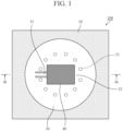
- FIG. 1 is a plan view illustrating the configuration of the antenna device 100 according to the first embodiment.
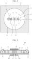
- FIG. 2 is a plan view illustrating a state in which an RF circuit 40 is removed from the antenna device 100.
- FIG. 3 is a cross-sectional view viewed along arrows III-III in FIG. 1 .
- the antenna device 100 includes a substrate 10, a GND conductor 20, GND pins 21, a patch conductor 30, a coplanar line 31, an RF circuit 40, mounted components 41a and 41b, a signal line 42, and a power supply line 43.
- the substrate 10 is formed of an insulating material such as resin, ceramic, or a hybrid material obtained by combining resin and ceramic.
- the substrate 10 has a rectangular shape in plan view and has a predetermined thickness.
- the GND conductor 20 is provided inside the substrate 10.
- the GND conductor 20 is provided between the top face of the substrate 10 and the lower face of the substrate 10.
- the GND conductor 20 is formed into a flat plate shape and has a size substantially equal to the size of the substrate 10.
- the patch conductor 30 is provided on the top face of the substrate 10. That is, the lower face of the patch conductor 30 is attached to the top face of the substrate 10.
- the patch conductor 30 has, for example, a circular shape.
- the patch conductor 30 is provided in such a manner as to face the GND conductor 20.
- the plurality of GND pins 21 is provided inside the substrate 10. These GND pins 21 connect the GND conductor 20 and the patch conductor 30.
- the coplanar line 31 is a conductor region surrounded by linear slits on three sides thereof in the patch conductor 30. In this manner, the coplanar line 31 is linearly formed on a region inside the three continuous slits in the patch conductor 30. In the coplanar line 31, a feeding point P connecting the patch conductor 30 and the RF circuit 40 is formed. Meanwhile, the GND pins 21 are connected to a region outside the three continuous slits in the patch conductor 30.
- the RF circuit 40 is provided at the central portion on the top face of the patch conductor 30. That is, the lower face of the RF circuit 40 is attached to the top face of the patch conductor 30.
- the RF circuit 40 is, for example, a low-noise amplifier circuit.
- the RF circuit 40 is surrounded by a plurality of GND pins 21 and shielded by the plurality of GND pins 21. In other words, the plurality of GND pins 21 prevent intrusion of radio waves from the outside of the antenna device 100 into the RF circuit 40 and leakage of noise from the RF circuit 40 to the outside of the antenna device 100.
- the RF circuit 40 is surrounded by a plurality of GND pins 21 farthest radially outward from the center of the patch conductor 30 among the plurality of GND pins 21.
- a radially inner region with respect to the plurality of GND pins 21 surrounding the circumference of the RF circuit 40 in this manner is hereinafter referred to as an inner region 32.
- the mounted components 41a and 41b are provided on the lower face of the substrate 10. That is, the top faces of the mounted components 41a and 41b are attached to the lower face of the substrate 10.
- the signal line 42 is provided inside the substrate 10.
- the signal line 42 connects the RF circuit 40 and the mounted component 41a.
- the signal line 42 penetrates through the GND conductor 20 and the patch conductor 30 without being in contact with them. Therefore, the mounted component 41a can receive a signal output from the RF circuit 40 via the signal line 42.
- the signal line 42 is surrounded by a plurality of GND pins 21 and shielded by the plurality of GNDs 21.
- the plurality of GND pins 21 prevents intrusion of radio waves from the outside of the antenna device 100 into the signal line 42 and leakage of noise from the signal line 42 to the outside of the antenna device 100.
- the power supply line 43 is provided inside the substrate 10.
- the power supply line 43 connects the RF circuit 40 and the mounted component 41b.
- the power supply line 43 penetrates through the GND conductor 20 and the patch conductor 30 without being in contact with them. Therefore, the mounted component 41b can supply power to the RF circuit 40 via the power supply line 43.
- the power supply line 43 is surrounded by a plurality of GND pins 21 and shielded by the plurality of GND pins 21.
- the plurality of GND pins 21 prevents intrusion of radio waves from the outside of the antenna device 100 into the power supply line 43 and leakage of noise from the power supply line 43 to the outside of the antenna device 100.
- the antenna device 100 operates as a reception antenna device.
- the patch conductor 30 when receiving a radio wave, the patch conductor 30 generates a high-frequency signal corresponding to the radio wave.
- the patch conductor 30 transmits the generated high-frequency signal to the RF circuit 40 via the coplanar line 31.
- the RF circuit 40 amplifies the high-frequency signal and transmits the amplified high-frequency signal to the mounted component 41a via the signal line 42.
- power supply to the RF circuit 40 is performed by the mounted component 41b to the RF circuit 40 via the power supply line 43.
- an arrow illustrated in FIG. 3 indicates the direction of a line of electric force L.
- no current flows in the inner region 32 surrounded by the GND pins 21 since the circumference of the inner region 32 is short-circuited by the GND pins 21. That is, the inner region 32 is shielded by the GND pins 21.
- the RF circuit 40, the signal line 42, and the power supply line 43 are provided in the inner region 32 surrounded by the GND pins 21. Therefore, intrusion of radio waves from the outside of the antenna device 100 into the RF circuit 40, the signal line 42, and the power supply line 43 provided in the inner region 32 is prevented.
- the inner region 32 of the patch conductor 30 is connected to the GND conductor 20 via a plurality of GND pins 21. Therefore, the antenna device 100 can use the inner region 32 as a mounting space for the RF circuit 40.
- the RF circuit 40 is used in a high-frequency band of several tens of GHz band.
- an installation face for installing the RF circuit 40 is a ground face (top face of the patch conductor 30) having a large wavelength ratio and no holes. Therefore, the antenna device 100 can reduce unnecessary coupling due to radio waves radiated from the antenna device 100 to the outside and the influence of noise from the outside of the antenna device 100.
- the antenna device 100 can also operate as a transmission antenna device. Even in a case where the antenna device 100 operates as a transmission antenna device, it is possible to achieve an effect equivalent to that in the case where the antenna device operates as a reception antenna device.
- the antenna device 100 includes: the patch conductor 30 provided on the substrate 10; the GND conductor 20 provided in the substrate 10 in such a manner as to face the patch conductor 30; the GND pins 21 that are provided in the substrate 10 and that connect the patch conductor 30 and the GND conductor 20; and the RF circuit 40 provided on a first face of the patch conductor 30 opposite to a second face of the patch conductor 30, the second face being attached to the substrate 10, the RF circuit 40 being provided in such a manner as to be surrounded by the GND pins 21. Therefore, the antenna device 100 does not require a space for installing the RF circuit 40 in a space inside the patch antenna, so that the size of the device can be reduced.
- FIG. 4 is a cross-sectional view illustrating the configuration of the antenna device 200 according to the second embodiment.
- the antenna device 200 according to the second embodiment has a configuration in which a shielding case 50 is added to the configuration of the antenna device 100 according to the first embodiment.
- the shielding case 50 is formed of a metal material.
- the shielding case 50 covers the circumference of the RF circuit 40.
- Such a shielding case 50 is electrically connected to the top face of the patch conductor 30 using, for example, solder, a conductive adhesive, or the like. That is, the shielding case 50 covers the outside of the entire RF circuit 40 with the patch conductor 30 serving as the GND. Moreover, the shielding case 50 is not electrically connected to the coplanar line 31.
- the shielding case 50 may cover the entire coplanar line 31 or partially cover the coplanar line 31.
- the shielding case 50 has a cutout portion that straddles the coplanar line 31 so as not to be in electrical contact with the coplanar line 31.
- the antenna device 200 can improve the shieldability of the RF circuit 40 by covering the RF circuit 40 with the shielding case 50 in the above manner. That is, the shielding case 50 prevents intrusion of radio waves from the outside of the antenna device 200 into the RF circuit 40 and leakage of noise from the RF circuit 40 to the outside of the antenna device 200.
- metal plating may be applied to the surface of the RF circuit 40 instead of including the shielding case 50.
- the surface of the metal-plated RF circuit 40 is short-circuited via the patch conductor 30.
- the antenna device 200 includes the shielding case 50 that covers the outside of the RF circuit 40 and that is connected to the patch conductor 30. Therefore, the antenna device 200 can improve the shieldability of the RF circuit 40.
- the surface of the RF circuit 40 is plated with metal. Therefore, the antenna device 200 can improve the shieldability of the RF circuit 40.
- FIG. 5 is a plan view illustrating the configuration of the antenna device 300 according to the third embodiment.
- the antenna device 300 according to the third embodiment has a configuration that includes two coplanar lines 31a and 31b instead of one coplanar line 31 in the antenna device 100 according to the first embodiment.
- the patch conductor 30 includes the coplanar lines 31a and 31b.
- the coplanar line 31a and the coplanar line 31b are provided in such a manner as to be perpendicular to each other.
- Each of the coplanar lines 31a and 31b has a feeding point P.
- the antenna device 300 can excite a circularly polarized wave by feeding power through the feeding points P of the coplanar lines 31a and 31b which have a phase difference of 90° therebetween as described above.
- the antenna device 300 may include three or more coplanar lines.
- the coplanar lines can be provided at desired positions by appropriately setting the phase differences between adjacent coplanar lines.
- the antenna device 300 includes two or more coplanar lines 31a and 31b that are provided for the patch conductor 30 and that connect the patch conductor 30 and the RF circuit 40.
- the two coplanar lines 31b and 31b are provided in such a manner as to be perpendicular to each other. Therefore, the antenna device 300 can excite a circularly polarized wave.
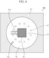
- FIG. 6 is a plan view illustrating the configuration of the antenna device 400 according to the fourth embodiment.
- the antenna device 400 according to the fourth embodiment has a configuration in which a cutout portion 30a is added to the configuration of the antenna device 100 according to the first embodiment.
- the patch conductor 30 has the cutout portion 30a.
- the cutout portion 30a is for implementing circular polarization.
- the antenna device 400 includes the cutout portion 30a provided in the outer circumferential portion of the patch conductor 30. Therefore, the antenna device 400 can implement circular polarization by the cutout portion 30a.
- FIG. 7 is a plan view illustrating the configuration of the antenna device 500 according to the fifth embodiment.
- the antenna device 500 according to the fifth embodiment has a configuration that includes a ⁇ /4 conversion line 33 instead of the coplanar line 31 of the antenna device 100 according to the first embodiment.
- the patch conductor 30 includes the ⁇ /4 conversion line 33.
- the ⁇ /4 conversion line 33 is a conductor region surrounded by slits on both sides in the width direction in the patch conductor 30.
- the ⁇ /4 conversion line 33 is formed into a rectangular shape in the inner portion between the slits facing each other in the patch conductor 30 as described above.
- the ⁇ /4 conversion line 33 connects the patch conductor 30 and the RF circuit 40. Therefore, the ⁇ /4 conversion line 33 facilitates impedance matching between the patch conductor 30 and the RF circuit 40 as compared with the case where the coplanar line 31 is provided.
- the line width of the ⁇ /4 conversion line 33 can be set desirably, the value of the impedance can be selected desirably. Therefore, in the antenna device 500, it is possible to design an antenna in which the patch conductor 30 and the RF circuit 40 are set to have desired impedance values.
- the antenna device 500 includes the rectangular ⁇ /4 conversion line 33, however, the shape of the ⁇ /4 conversion line 33 is not limited thereto.
- the ⁇ /4 conversion line 33 may have, for example, a tapered shape in which the line width gradually increases as it is closer to an outer side in the radial direction of the patch conductor 30.
- the antenna device 500 can reduce the influence on a reflection coefficient of a radio wave due to a steep change in the line width.
- the antenna device 500 may include a plurality of ⁇ /4 conversion lines 33.
- the ⁇ /4 conversion lines 33 can be provided at desired positions by appropriately setting phase differences between adjacent ⁇ /4 conversion lines 33.
- the antenna device 500 includes the ⁇ /4 conversion line 33 that is provided for the patch conductor 30 and that connects the patch conductor 30 and the RF circuit 40.
- the ⁇ /4 conversion line 33 is formed in such a manner that a portion closer to the outside of the patch conductor 30 has a wider line width. Therefore, in the antenna device 500, it is possible to set the patch conductor 30 and the RF circuit 40 to have desired impedance values.
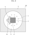
- FIG. 8 is a plan view illustrating the configuration of the antenna device 600 according to the sixth embodiment.
- the antenna device 600 according to the sixth embodiment has a configuration that includes a feed line 34 instead of the coplanar line 31 of the antenna device 100 according to the first embodiment.
- the patch conductor 30 includes the feed line 34.
- the feed line 34 is a conductor region that is a portion remaining after cutting out parts of the patch conductor 30. Two portions obtained by cutting out the parts from the patch conductor 30 are hollow portions 30b. Furthermore, a part of the feed line 34 forms a microstrip line. As described above, a part of the feed line 34 is a microstrip line, and thus impedance matching between the patch conductor 30 and the RF circuit 40 is easily achieved by providing a stub in the feed line 34, for example.
- the antenna device 600 may include a plurality of feed lines 34.
- the feed lines 34 can be provided at desired positions by appropriately setting phase differences between adjacent feed lines 34.
- the antenna device 600 includes the feed line 34 that is provided for the patch conductor 30 and that connects the patch conductor 30 and the RF circuit 40.
- the feed line 34 is formed by cutting out parts of the patch conductor 30. Therefore, in the antenna device 600, the values of impedance can be easily matched between the patch conductor 30 and the RF circuit 40.
- the present disclosure can include a flexible combination of the embodiments, modification of any component of the embodiments, or omission of any component in the embodiments within the scope of the disclosure.
- an antenna device includes an RF circuit provided in such a manner as to be surrounded by GND pins, a space for installing the RF circuit is not required in a space inside the patch antenna, so that the size of the device can be reduced. Therefore, the antenna device is suitable for use as an antenna device or the like.
Landscapes
- Physics & Mathematics (AREA)
- Electromagnetism (AREA)
- Waveguide Aerials (AREA)
- Variable-Direction Aerials And Aerial Arrays (AREA)
Abstract
Description
- The present disclosure relates to an antenna device.
- In some antenna devices, components of an RF circuit are installed inside an antenna unit. Such a conventional antenna device is disclosed in, for example, Patent Literature 1.
- Patent Literature 1:
JP 2001-339239 A - In the antenna device disclosed in Patent Literature 1, components of an RF circuit are provided in a space inside an annular patch antenna including a patch conductor and a GND conductor. For this reason, in the antenna device disclosed in Patent Literature 1, the patch conductor and the GND conductor are larger than necessary, which may lead to an increase in size of the device.
- The present disclosure has been made to solve the above problem, and an object of the present disclosure is to provide an antenna device that does not require a space for installing an RF circuit in the space inside the patch antenna, so that the size of the device can be reduced.
- An antenna device according to the present disclosure includes: a patch conductor provided on a substrate; a GND conductor provided in the substrate in such a manner as to face the patch conductor; GND pins that are provided in the substrate and that connect the patch conductor and the GND conductor; and an RF circuit provided on a first face of the patch conductor opposite to a second face of the patch conductor, the second face being attached to the substrate, the RF circuit being provided in such a manner as to be surrounded by the GND pins.
- According to the present disclosure, with the above configuration, it is possible to downsize the device since a space for installing an RF circuit is not required in a space inside a patch antenna.
-
-
FIG. 1 is a plan view illustrating a configuration of an antenna device according to a first embodiment. -
FIG. 2 is a plan view illustrating a state in which an RF circuit is removed from the antenna device. -
FIG. 3 is a cross-sectional view viewed along arrows III-III inFIG. 1 . -
FIG. 4 is a cross-sectional view illustrating a configuration of an antenna device according to a second embodiment. -
FIG. 5 is a plan view illustrating a configuration of an antenna device according to a third embodiment. -
FIG. 6 is a plan view illustrating a configuration of an antenna device according to a fourth embodiment. -
FIG. 7 is a plan view illustrating a configuration of an antenna device according to a fifth embodiment. -
FIG. 8 is a plan view illustrating a configuration of an antenna device according to a sixth embodiment. - To describe the present disclosure further in detail, embodiments for carrying out the present disclosure will be described below with reference to the accompanying drawings.
- An
antenna device 100 according to a first embodiment will be described with reference toFIGS. 1 to 3 .FIG. 1 is a plan view illustrating the configuration of theantenna device 100 according to the first embodiment.FIG. 2 is a plan view illustrating a state in which anRF circuit 40 is removed from theantenna device 100.FIG. 3 is a cross-sectional view viewed along arrows III-III inFIG. 1 . - The
antenna device 100 includes asubstrate 10, aGND conductor 20,GND pins 21, apatch conductor 30, acoplanar line 31, anRF circuit 40, mountedcomponents signal line 42, and apower supply line 43. - The
substrate 10 is formed of an insulating material such as resin, ceramic, or a hybrid material obtained by combining resin and ceramic. Thesubstrate 10 has a rectangular shape in plan view and has a predetermined thickness. - The
GND conductor 20 is provided inside thesubstrate 10. TheGND conductor 20 is provided between the top face of thesubstrate 10 and the lower face of thesubstrate 10. TheGND conductor 20 is formed into a flat plate shape and has a size substantially equal to the size of thesubstrate 10. - The
patch conductor 30 is provided on the top face of thesubstrate 10. That is, the lower face of thepatch conductor 30 is attached to the top face of thesubstrate 10. Thepatch conductor 30 has, for example, a circular shape. Thepatch conductor 30 is provided in such a manner as to face theGND conductor 20. - The plurality of
GND pins 21 is provided inside thesubstrate 10. TheseGND pins 21 connect theGND conductor 20 and thepatch conductor 30. - The
coplanar line 31 is a conductor region surrounded by linear slits on three sides thereof in thepatch conductor 30. In this manner, thecoplanar line 31 is linearly formed on a region inside the three continuous slits in thepatch conductor 30. In thecoplanar line 31, a feeding point P connecting thepatch conductor 30 and theRF circuit 40 is formed. Meanwhile, theGND pins 21 are connected to a region outside the three continuous slits in thepatch conductor 30. - The
RF circuit 40 is provided at the central portion on the top face of thepatch conductor 30. That is, the lower face of theRF circuit 40 is attached to the top face of thepatch conductor 30. TheRF circuit 40 is, for example, a low-noise amplifier circuit. TheRF circuit 40 is surrounded by a plurality ofGND pins 21 and shielded by the plurality ofGND pins 21. In other words, the plurality ofGND pins 21 prevent intrusion of radio waves from the outside of theantenna device 100 into theRF circuit 40 and leakage of noise from theRF circuit 40 to the outside of theantenna device 100. - Note that the
RF circuit 40 is surrounded by a plurality ofGND pins 21 farthest radially outward from the center of thepatch conductor 30 among the plurality ofGND pins 21. A radially inner region with respect to the plurality ofGND pins 21 surrounding the circumference of theRF circuit 40 in this manner is hereinafter referred to as aninner region 32. - The mounted
components substrate 10. That is, the top faces of the mountedcomponents substrate 10. - The
signal line 42 is provided inside thesubstrate 10. Thesignal line 42 connects theRF circuit 40 and the mountedcomponent 41a. Incidentally, thesignal line 42 penetrates through theGND conductor 20 and thepatch conductor 30 without being in contact with them. Therefore, the mountedcomponent 41a can receive a signal output from theRF circuit 40 via thesignal line 42. - Moreover, the
signal line 42 is surrounded by a plurality ofGND pins 21 and shielded by the plurality ofGNDs 21. In other words, the plurality ofGND pins 21 prevents intrusion of radio waves from the outside of theantenna device 100 into thesignal line 42 and leakage of noise from thesignal line 42 to the outside of theantenna device 100. - The
power supply line 43 is provided inside thesubstrate 10. Thepower supply line 43 connects theRF circuit 40 and the mountedcomponent 41b. Incidentally, thepower supply line 43 penetrates through theGND conductor 20 and thepatch conductor 30 without being in contact with them. Therefore, the mountedcomponent 41b can supply power to theRF circuit 40 via thepower supply line 43. - Moreover, the
power supply line 43 is surrounded by a plurality of GND pins 21 and shielded by the plurality of GND pins 21. In other words, the plurality of GND pins 21 prevents intrusion of radio waves from the outside of theantenna device 100 into thepower supply line 43 and leakage of noise from thepower supply line 43 to the outside of theantenna device 100. - Next, a case where the
antenna device 100 operates as a reception antenna device will be described. - First, when receiving a radio wave, the
patch conductor 30 generates a high-frequency signal corresponding to the radio wave. Next, thepatch conductor 30 transmits the generated high-frequency signal to theRF circuit 40 via thecoplanar line 31. In this case, theRF circuit 40 amplifies the high-frequency signal and transmits the amplified high-frequency signal to the mountedcomponent 41a via thesignal line 42. In addition, power supply to theRF circuit 40 is performed by the mountedcomponent 41b to theRF circuit 40 via thepower supply line 43. - Incidentally, an arrow illustrated in
FIG. 3 indicates the direction of a line of electric force L. As illustrated inFIG. 3 , no current flows in theinner region 32 surrounded by the GND pins 21 since the circumference of theinner region 32 is short-circuited by the GND pins 21. That is, theinner region 32 is shielded by the GND pins 21. In theantenna device 100, theRF circuit 40, thesignal line 42, and thepower supply line 43 are provided in theinner region 32 surrounded by the GND pins 21. Therefore, intrusion of radio waves from the outside of theantenna device 100 into theRF circuit 40, thesignal line 42, and thepower supply line 43 provided in theinner region 32 is prevented. - Furthermore, the
inner region 32 of thepatch conductor 30 is connected to theGND conductor 20 via a plurality of GND pins 21. Therefore, theantenna device 100 can use theinner region 32 as a mounting space for theRF circuit 40. - It is based on the premise that the
RF circuit 40 is used in a high-frequency band of several tens of GHz band. In theantenna device 100, in the high-frequency band, an installation face for installing theRF circuit 40 is a ground face (top face of the patch conductor 30) having a large wavelength ratio and no holes. Therefore, theantenna device 100 can reduce unnecessary coupling due to radio waves radiated from theantenna device 100 to the outside and the influence of noise from the outside of theantenna device 100. - Note that the above description of the operation of the
antenna device 100 relates to a case where theantenna device 100 operates as a reception antenna device, however, theantenna device 100 can also operate as a transmission antenna device. Even in a case where theantenna device 100 operates as a transmission antenna device, it is possible to achieve an effect equivalent to that in the case where the antenna device operates as a reception antenna device. - As described above, the
antenna device 100 according to the first embodiment includes: thepatch conductor 30 provided on thesubstrate 10; theGND conductor 20 provided in thesubstrate 10 in such a manner as to face thepatch conductor 30; the GND pins 21 that are provided in thesubstrate 10 and that connect thepatch conductor 30 and theGND conductor 20; and theRF circuit 40 provided on a first face of thepatch conductor 30 opposite to a second face of thepatch conductor 30, the second face being attached to thesubstrate 10, theRF circuit 40 being provided in such a manner as to be surrounded by the GND pins 21. Therefore, theantenna device 100 does not require a space for installing theRF circuit 40 in a space inside the patch antenna, so that the size of the device can be reduced. - An
antenna device 200 according to a second embodiment will be described with reference toFIG. 4. FIG. 4 is a cross-sectional view illustrating the configuration of theantenna device 200 according to the second embodiment. - As illustrated in
FIG. 4 , theantenna device 200 according to the second embodiment has a configuration in which ashielding case 50 is added to the configuration of theantenna device 100 according to the first embodiment. - The shielding
case 50 is formed of a metal material. The shieldingcase 50 covers the circumference of theRF circuit 40. Such a shieldingcase 50 is electrically connected to the top face of thepatch conductor 30 using, for example, solder, a conductive adhesive, or the like. That is, the shieldingcase 50 covers the outside of theentire RF circuit 40 with thepatch conductor 30 serving as the GND. Moreover, the shieldingcase 50 is not electrically connected to thecoplanar line 31. - Specifically, as long as the shielding
case 50 covers theentire RF circuit 40, the shieldingcase 50 may cover the entirecoplanar line 31 or partially cover thecoplanar line 31. In a case where the shieldingcase 50 partially covers thecoplanar line 31, the shieldingcase 50 has a cutout portion that straddles thecoplanar line 31 so as not to be in electrical contact with thecoplanar line 31. - The
antenna device 200 can improve the shieldability of theRF circuit 40 by covering theRF circuit 40 with the shieldingcase 50 in the above manner. That is, the shieldingcase 50 prevents intrusion of radio waves from the outside of theantenna device 200 into theRF circuit 40 and leakage of noise from theRF circuit 40 to the outside of theantenna device 200. - Note that, in the
antenna device 200, metal plating may be applied to the surface of theRF circuit 40 instead of including the shieldingcase 50. In this case, the surface of the metal-platedRF circuit 40 is short-circuited via thepatch conductor 30. By metalizing the surface of theRF circuit 40 in this manner, the shieldability of theRF circuit 40 can be improved in theantenna device 200. - As described above, the
antenna device 200 according to the second embodiment includes the shieldingcase 50 that covers the outside of theRF circuit 40 and that is connected to thepatch conductor 30. Therefore, theantenna device 200 can improve the shieldability of theRF circuit 40. - Furthermore, in the
antenna device 200, the surface of theRF circuit 40 is plated with metal. Therefore, theantenna device 200 can improve the shieldability of theRF circuit 40. - An
antenna device 300 according to a third embodiment will be described with reference toFIG. 5. FIG. 5 is a plan view illustrating the configuration of theantenna device 300 according to the third embodiment. - As illustrated in
FIG. 5 , theantenna device 300 according to the third embodiment has a configuration that includes twocoplanar lines coplanar line 31 in theantenna device 100 according to the first embodiment. - The
patch conductor 30 includes thecoplanar lines coplanar line 31a and thecoplanar line 31b are provided in such a manner as to be perpendicular to each other. Each of thecoplanar lines antenna device 300 can excite a circularly polarized wave by feeding power through the feeding points P of thecoplanar lines - Note that the
antenna device 300 may include three or more coplanar lines. In this case, in theantenna device 300, the coplanar lines can be provided at desired positions by appropriately setting the phase differences between adjacent coplanar lines. - As described above, the
antenna device 300 according to the third embodiment includes two or morecoplanar lines patch conductor 30 and that connect thepatch conductor 30 and theRF circuit 40. The twocoplanar lines antenna device 300 can excite a circularly polarized wave. - An
antenna device 400 according to a fourth embodiment will be described with reference toFIG. 6. FIG. 6 is a plan view illustrating the configuration of theantenna device 400 according to the fourth embodiment. - The
antenna device 400 according to the fourth embodiment has a configuration in which acutout portion 30a is added to the configuration of theantenna device 100 according to the first embodiment. - As illustrated in
FIG. 6 , thepatch conductor 30 has thecutout portion 30a. Thecutout portion 30a is for implementing circular polarization. - As described above, the
antenna device 400 according to the fourth embodiment includes thecutout portion 30a provided in the outer circumferential portion of thepatch conductor 30. Therefore, theantenna device 400 can implement circular polarization by thecutout portion 30a. - An
antenna device 500 according to a fifth embodiment will be described with reference toFIG. 7. FIG. 7 is a plan view illustrating the configuration of theantenna device 500 according to the fifth embodiment. - The
antenna device 500 according to the fifth embodiment has a configuration that includes a λ/4conversion line 33 instead of thecoplanar line 31 of theantenna device 100 according to the first embodiment. - As illustrated in
FIG. 7 , thepatch conductor 30 includes the λ/4conversion line 33. The λ/4conversion line 33 is a conductor region surrounded by slits on both sides in the width direction in thepatch conductor 30. The λ/4conversion line 33 is formed into a rectangular shape in the inner portion between the slits facing each other in thepatch conductor 30 as described above. The λ/4conversion line 33 connects thepatch conductor 30 and theRF circuit 40. Therefore, the λ/4conversion line 33 facilitates impedance matching between thepatch conductor 30 and theRF circuit 40 as compared with the case where thecoplanar line 31 is provided. - In addition, since the line width of the λ/4
conversion line 33 can be set desirably, the value of the impedance can be selected desirably. Therefore, in theantenna device 500, it is possible to design an antenna in which thepatch conductor 30 and theRF circuit 40 are set to have desired impedance values. - Note that the
antenna device 500 includes the rectangular λ/4conversion line 33, however, the shape of the λ/4conversion line 33 is not limited thereto. The λ/4conversion line 33 may have, for example, a tapered shape in which the line width gradually increases as it is closer to an outer side in the radial direction of thepatch conductor 30. By including the tapered λ/4conversion line 33, theantenna device 500 can reduce the influence on a reflection coefficient of a radio wave due to a steep change in the line width. - Furthermore, the
antenna device 500 may include a plurality of λ/4 conversion lines 33. In this case, in theantenna device 500, the λ/4conversion lines 33 can be provided at desired positions by appropriately setting phase differences between adjacent λ/4 conversion lines 33. - As described above, the
antenna device 500 according to the fifth embodiment includes the λ/4conversion line 33 that is provided for thepatch conductor 30 and that connects thepatch conductor 30 and theRF circuit 40. The λ/4conversion line 33 is formed in such a manner that a portion closer to the outside of thepatch conductor 30 has a wider line width. Therefore, in theantenna device 500, it is possible to set thepatch conductor 30 and theRF circuit 40 to have desired impedance values. - An
antenna device 600 according to a sixth embodiment will be described with reference toFIG. 8. FIG. 8 is a plan view illustrating the configuration of theantenna device 600 according to the sixth embodiment. - The
antenna device 600 according to the sixth embodiment has a configuration that includes afeed line 34 instead of thecoplanar line 31 of theantenna device 100 according to the first embodiment. - As illustrated in
FIG. 8 , thepatch conductor 30 includes thefeed line 34. Thefeed line 34 is a conductor region that is a portion remaining after cutting out parts of thepatch conductor 30. Two portions obtained by cutting out the parts from thepatch conductor 30 arehollow portions 30b. Furthermore, a part of thefeed line 34 forms a microstrip line. As described above, a part of thefeed line 34 is a microstrip line, and thus impedance matching between thepatch conductor 30 and theRF circuit 40 is easily achieved by providing a stub in thefeed line 34, for example. - Note that the
antenna device 600 may include a plurality of feed lines 34. In this case, in theantenna device 600, thefeed lines 34 can be provided at desired positions by appropriately setting phase differences between adjacent feed lines 34. - As described above, the
antenna device 600 according to the sixth embodiment includes thefeed line 34 that is provided for thepatch conductor 30 and that connects thepatch conductor 30 and theRF circuit 40. Thefeed line 34 is formed by cutting out parts of thepatch conductor 30. Therefore, in theantenna device 600, the values of impedance can be easily matched between thepatch conductor 30 and theRF circuit 40. - Note that the present disclosure can include a flexible combination of the embodiments, modification of any component of the embodiments, or omission of any component in the embodiments within the scope of the disclosure.
- Since an antenna device according to the present disclosure includes an RF circuit provided in such a manner as to be surrounded by GND pins, a space for installing the RF circuit is not required in a space inside the patch antenna, so that the size of the device can be reduced. Therefore, the antenna device is suitable for use as an antenna device or the like.
- 10: substrate, 20: GND conductor, 21: GND pin, 30: patch conductor, 30a: cutout portion, 30b: hollow portion, 31, 31a, 31b: coplanar line, 32: inner region, 33: λ/4 conversion line, 34: feed line, 40: RF circuit, 41a, 41b: mounted component, 42: signal line, 43: power supply line, 50: shielding case, 100 to 600: antenna device, P: feeding point, L: line of electric force
Claims (7)
- An antenna device comprising:a patch conductor provided on a substrate;a GND conductor provided in the substrate in such a manner as to face the patch conductor;GND pins that are provided in the substrate and that connect the patch conductor and the GND conductor; andan RF circuit provided on a first face of the patch conductor opposite to a second face of the patch conductor, the second face being attached to the substrate, the RF circuit being provided in such a manner as to be surrounded by the GND pins.
- The antenna device according to claim 1, further comprising:
a shielding case that covers an outside of the RF circuit and that is connected to the patch conductor. - The antenna device according to claim 1,
wherein a surface of the RF circuit is plated with metal. - The antenna device according to claim 1, further comprising:two or more coplanar lines that are provided for the patch conductor and that connect the patch conductor and the RF circuit,wherein the two coplanar lines are provided in such a manner as to be perpendicular to each other.
- The antenna device according to claim 1, further comprising:
a cutout portion provided in an outer circumferential portion of the patch conductor. - The antenna device according to claim 1, further comprising:a λ/4 conversion line that is provided for the patch conductor and that connects the patch conductor and the RF circuit,wherein the λ/4 conversion line is formed in such a manner that a portion closer to an outside of the patch conductor has a wider line width.
- The antenna device according to claim 1, further comprising:a feed line that is provided for the patch conductor and that connects the patch conductor and the RF circuit,wherein the feed line is formed by cutting out a part of the patch conductor.
Applications Claiming Priority (1)
| Application Number | Priority Date | Filing Date | Title |
|---|---|---|---|
| PCT/JP2020/047405 WO2022130613A1 (en) | 2020-12-18 | 2020-12-18 | Antenna device |
Publications (3)
| Publication Number | Publication Date |
|---|---|
| EP4243201A1 true EP4243201A1 (en) | 2023-09-13 |
| EP4243201A4 EP4243201A4 (en) | 2023-12-13 |
| EP4243201B1 EP4243201B1 (en) | 2025-09-03 |
Family
ID=82059318
Family Applications (1)
| Application Number | Title | Priority Date | Filing Date |
|---|---|---|---|
| EP20966000.0A Active EP4243201B1 (en) | 2020-12-18 | 2020-12-18 | Antenna device |
Country Status (4)
| Country | Link |
|---|---|
| US (1) | US12199360B2 (en) |
| EP (1) | EP4243201B1 (en) |
| JP (1) | JP7246583B2 (en) |
| WO (1) | WO2022130613A1 (en) |
Family Cites Families (8)
| Publication number | Priority date | Publication date | Assignee | Title |
|---|---|---|---|---|
| JP2001339239A (en) | 2000-05-29 | 2001-12-07 | Tdk Corp | Antenna unit |
| JP3995206B2 (en) | 2002-12-20 | 2007-10-24 | Tdk株式会社 | Module with antenna |
| TWI518991B (en) * | 2013-02-08 | 2016-01-21 | 巽晨國際股份有限公司 | Integrated antenna and integrated circuit components of the shielding module |
| US20140266959A1 (en) * | 2013-03-15 | 2014-09-18 | City University Of Hong Kong | Patch antenna |
| JP6674824B2 (en) | 2016-04-05 | 2020-04-01 | 株式会社ユーシン | Multilayer substrate circuit module, wireless communication device and radar device |
| NO347324B1 (en) | 2017-02-08 | 2023-09-18 | Norbit Its | Patch antenna |
| JP6661714B2 (en) | 2018-03-08 | 2020-03-11 | シャープ株式会社 | Microwave equipment |
| CN109273837A (en) * | 2018-09-03 | 2019-01-25 | 北京邮电大学 | A structure for realizing nesting connection between antenna and circuit |
-
2020
- 2020-12-18 WO PCT/JP2020/047405 patent/WO2022130613A1/en not_active Ceased
- 2020-12-18 EP EP20966000.0A patent/EP4243201B1/en active Active
- 2020-12-18 JP JP2022568688A patent/JP7246583B2/en active Active
-
2023
- 2023-03-22 US US18/124,867 patent/US12199360B2/en active Active
Also Published As
| Publication number | Publication date |
|---|---|
| US20230223694A1 (en) | 2023-07-13 |
| JPWO2022130613A1 (en) | 2022-06-23 |
| US12199360B2 (en) | 2025-01-14 |
| EP4243201B1 (en) | 2025-09-03 |
| EP4243201A4 (en) | 2023-12-13 |
| WO2022130613A1 (en) | 2022-06-23 |
| JP7246583B2 (en) | 2023-03-27 |
Similar Documents
| Publication | Publication Date | Title |
|---|---|---|
| US9190732B2 (en) | Antenna device | |
| US10418708B2 (en) | Wideband antenna | |
| US9577340B2 (en) | Waveguide adapter plate to facilitate accurate alignment of sectioned waveguide channel in microwave antenna assembly | |
| US10971824B2 (en) | Antenna element | |
| US11936096B2 (en) | Wiring substrate, antenna module, and communication device | |
| US9515385B2 (en) | Coplanar waveguide implementing launcher and waveguide channel section in IC package substrate | |
| US9419341B2 (en) | RF system-in-package with quasi-coaxial coplanar waveguide transition | |
| JP5431433B2 (en) | High frequency line-waveguide converter | |
| US7248224B2 (en) | Antenna device having radiation characteristics suitable for ultrawideband communications | |
| US11303004B2 (en) | Microstrip-to-waveguide transition including a substrate integrated waveguide with a 90 degree bend section | |
| US10461403B2 (en) | Antenna device | |
| US20200333430A1 (en) | Antenna with Anti-Interference Arrangement and Manufacturing Method Thereof | |
| JPWO2014122925A1 (en) | Antenna device | |
| US9450282B2 (en) | Connection structure between a waveguide and a substrate, where the substrate has an opening larger than a waveguide opening | |
| US12199360B2 (en) | Antenna device | |
| US12107352B2 (en) | Antenna for sending and/or receiving electromagnetic signals | |
| JP5562080B2 (en) | antenna | |
| US11532865B2 (en) | PCB antenna, electronic circuit and item of electronic equipment provided with such an antenna | |
| JP2004320431A (en) | Planar antenna device | |
| US11211712B1 (en) | Compact integrated GNSS-UHF antenna system | |
| US20110169710A1 (en) | Cross-polarized antenna | |
| WO2017168705A1 (en) | Antenna | |
| JP6560623B2 (en) | Antenna device | |
| JP2018182362A (en) | Antenna device | |
| US20160079673A1 (en) | Chip Antenna Module |
Legal Events
| Date | Code | Title | Description |
|---|---|---|---|
| STAA | Information on the status of an ep patent application or granted ep patent |
Free format text: STATUS: THE INTERNATIONAL PUBLICATION HAS BEEN MADE |
|
| PUAI | Public reference made under article 153(3) epc to a published international application that has entered the european phase |
Free format text: ORIGINAL CODE: 0009012 |
|
| STAA | Information on the status of an ep patent application or granted ep patent |
Free format text: STATUS: REQUEST FOR EXAMINATION WAS MADE |
|
| 17P | Request for examination filed |
Effective date: 20230606 |
|
| AK | Designated contracting states |
Kind code of ref document: A1 Designated state(s): AL AT BE BG CH CY CZ DE DK EE ES FI FR GB GR HR HU IE IS IT LI LT LU LV MC MK MT NL NO PL PT RO RS SE SI SK SM TR |
|
| A4 | Supplementary search report drawn up and despatched |
Effective date: 20231114 |
|
| RIC1 | Information provided on ipc code assigned before grant |
Ipc: H01Q 23/00 20060101ALI20231108BHEP Ipc: H01Q 9/04 20060101ALI20231108BHEP Ipc: H01Q 1/52 20060101ALI20231108BHEP Ipc: H01Q 1/24 20060101AFI20231108BHEP |
|
| DAV | Request for validation of the european patent (deleted) | ||
| DAX | Request for extension of the european patent (deleted) | ||
| STAA | Information on the status of an ep patent application or granted ep patent |
Free format text: STATUS: EXAMINATION IS IN PROGRESS |
|
| 17Q | First examination report despatched |
Effective date: 20240805 |
|
| GRAP | Despatch of communication of intention to grant a patent |
Free format text: ORIGINAL CODE: EPIDOSNIGR1 |
|
| STAA | Information on the status of an ep patent application or granted ep patent |
Free format text: STATUS: GRANT OF PATENT IS INTENDED |
|
| INTG | Intention to grant announced |
Effective date: 20250327 |
|
| GRAS | Grant fee paid |
Free format text: ORIGINAL CODE: EPIDOSNIGR3 |
|
| GRAA | (expected) grant |
Free format text: ORIGINAL CODE: 0009210 |
|
| STAA | Information on the status of an ep patent application or granted ep patent |
Free format text: STATUS: THE PATENT HAS BEEN GRANTED |
|
| AK | Designated contracting states |
Kind code of ref document: B1 Designated state(s): AL AT BE BG CH CY CZ DE DK EE ES FI FR GB GR HR HU IE IS IT LI LT LU LV MC MK MT NL NO PL PT RO RS SE SI SK SM TR |
|
| REG | Reference to a national code |
Ref country code: CH Ref legal event code: EP |
|
| REG | Reference to a national code |
Ref country code: DE Ref legal event code: R096 Ref document number: 602020058329 Country of ref document: DE |
|
| REG | Reference to a national code |
Ref country code: IE Ref legal event code: FG4D |
|
| REG | Reference to a national code |
Ref country code: NL Ref legal event code: MP Effective date: 20250903 |
|
| PGFP | Annual fee paid to national office [announced via postgrant information from national office to epo] |
Ref country code: DE Payment date: 20251028 Year of fee payment: 6 |
|
| PGFP | Annual fee paid to national office [announced via postgrant information from national office to epo] |
Ref country code: GB Payment date: 20251030 Year of fee payment: 6 |
|
| PG25 | Lapsed in a contracting state [announced via postgrant information from national office to epo] |
Ref country code: NO Free format text: LAPSE BECAUSE OF FAILURE TO SUBMIT A TRANSLATION OF THE DESCRIPTION OR TO PAY THE FEE WITHIN THE PRESCRIBED TIME-LIMIT Effective date: 20251203 |
|
| REG | Reference to a national code |
Ref country code: LT Ref legal event code: MG9D |
|
| PG25 | Lapsed in a contracting state [announced via postgrant information from national office to epo] |
Ref country code: FI Free format text: LAPSE BECAUSE OF FAILURE TO SUBMIT A TRANSLATION OF THE DESCRIPTION OR TO PAY THE FEE WITHIN THE PRESCRIBED TIME-LIMIT Effective date: 20250903 |
|
| PGFP | Annual fee paid to national office [announced via postgrant information from national office to epo] |
Ref country code: IT Payment date: 20251121 Year of fee payment: 6 |
|
| PG25 | Lapsed in a contracting state [announced via postgrant information from national office to epo] |
Ref country code: HR Free format text: LAPSE BECAUSE OF FAILURE TO SUBMIT A TRANSLATION OF THE DESCRIPTION OR TO PAY THE FEE WITHIN THE PRESCRIBED TIME-LIMIT Effective date: 20250903 |
|
| PGFP | Annual fee paid to national office [announced via postgrant information from national office to epo] |
Ref country code: FR Payment date: 20251117 Year of fee payment: 6 |
|
| PG25 | Lapsed in a contracting state [announced via postgrant information from national office to epo] |
Ref country code: GR Free format text: LAPSE BECAUSE OF FAILURE TO SUBMIT A TRANSLATION OF THE DESCRIPTION OR TO PAY THE FEE WITHIN THE PRESCRIBED TIME-LIMIT Effective date: 20251204 |
|
| PG25 | Lapsed in a contracting state [announced via postgrant information from national office to epo] |
Ref country code: SE Free format text: LAPSE BECAUSE OF FAILURE TO SUBMIT A TRANSLATION OF THE DESCRIPTION OR TO PAY THE FEE WITHIN THE PRESCRIBED TIME-LIMIT Effective date: 20250903 |
|
| PG25 | Lapsed in a contracting state [announced via postgrant information from national office to epo] |
Ref country code: LV Free format text: LAPSE BECAUSE OF FAILURE TO SUBMIT A TRANSLATION OF THE DESCRIPTION OR TO PAY THE FEE WITHIN THE PRESCRIBED TIME-LIMIT Effective date: 20250903 |
|
| PG25 | Lapsed in a contracting state [announced via postgrant information from national office to epo] |
Ref country code: BG Free format text: LAPSE BECAUSE OF FAILURE TO SUBMIT A TRANSLATION OF THE DESCRIPTION OR TO PAY THE FEE WITHIN THE PRESCRIBED TIME-LIMIT Effective date: 20250903 Ref country code: PL Free format text: LAPSE BECAUSE OF FAILURE TO SUBMIT A TRANSLATION OF THE DESCRIPTION OR TO PAY THE FEE WITHIN THE PRESCRIBED TIME-LIMIT Effective date: 20250903 |
|
| PG25 | Lapsed in a contracting state [announced via postgrant information from national office to epo] |
Ref country code: RS Free format text: LAPSE BECAUSE OF FAILURE TO SUBMIT A TRANSLATION OF THE DESCRIPTION OR TO PAY THE FEE WITHIN THE PRESCRIBED TIME-LIMIT Effective date: 20251203 |
|
| PG25 | Lapsed in a contracting state [announced via postgrant information from national office to epo] |
Ref country code: ES Free format text: LAPSE BECAUSE OF FAILURE TO SUBMIT A TRANSLATION OF THE DESCRIPTION OR TO PAY THE FEE WITHIN THE PRESCRIBED TIME-LIMIT Effective date: 20250903 |
|
| REG | Reference to a national code |
Ref country code: AT Ref legal event code: MK05 Ref document number: 1834290 Country of ref document: AT Kind code of ref document: T Effective date: 20250903 |
|
| PG25 | Lapsed in a contracting state [announced via postgrant information from national office to epo] |
Ref country code: NL Free format text: LAPSE BECAUSE OF FAILURE TO SUBMIT A TRANSLATION OF THE DESCRIPTION OR TO PAY THE FEE WITHIN THE PRESCRIBED TIME-LIMIT Effective date: 20250903 |
|
| PG25 | Lapsed in a contracting state [announced via postgrant information from national office to epo] |
Ref country code: SM Free format text: LAPSE BECAUSE OF FAILURE TO SUBMIT A TRANSLATION OF THE DESCRIPTION OR TO PAY THE FEE WITHIN THE PRESCRIBED TIME-LIMIT Effective date: 20250903 |
|
| PG25 | Lapsed in a contracting state [announced via postgrant information from national office to epo] |
Ref country code: AT Free format text: LAPSE BECAUSE OF FAILURE TO SUBMIT A TRANSLATION OF THE DESCRIPTION OR TO PAY THE FEE WITHIN THE PRESCRIBED TIME-LIMIT Effective date: 20250903 |
|
| PG25 | Lapsed in a contracting state [announced via postgrant information from national office to epo] |
Ref country code: RO Free format text: LAPSE BECAUSE OF FAILURE TO SUBMIT A TRANSLATION OF THE DESCRIPTION OR TO PAY THE FEE WITHIN THE PRESCRIBED TIME-LIMIT Effective date: 20250903 |
|
| PG25 | Lapsed in a contracting state [announced via postgrant information from national office to epo] |
Ref country code: IS Free format text: LAPSE BECAUSE OF FAILURE TO SUBMIT A TRANSLATION OF THE DESCRIPTION OR TO PAY THE FEE WITHIN THE PRESCRIBED TIME-LIMIT Effective date: 20260103 |
|
| PG25 | Lapsed in a contracting state [announced via postgrant information from national office to epo] |
Ref country code: CZ Free format text: LAPSE BECAUSE OF FAILURE TO SUBMIT A TRANSLATION OF THE DESCRIPTION OR TO PAY THE FEE WITHIN THE PRESCRIBED TIME-LIMIT Effective date: 20250903 Ref country code: PT Free format text: LAPSE BECAUSE OF FAILURE TO SUBMIT A TRANSLATION OF THE DESCRIPTION OR TO PAY THE FEE WITHIN THE PRESCRIBED TIME-LIMIT Effective date: 20260105 |
|
| PG25 | Lapsed in a contracting state [announced via postgrant information from national office to epo] |
Ref country code: EE Free format text: LAPSE BECAUSE OF FAILURE TO SUBMIT A TRANSLATION OF THE DESCRIPTION OR TO PAY THE FEE WITHIN THE PRESCRIBED TIME-LIMIT Effective date: 20250903 Ref country code: SK Free format text: LAPSE BECAUSE OF FAILURE TO SUBMIT A TRANSLATION OF THE DESCRIPTION OR TO PAY THE FEE WITHIN THE PRESCRIBED TIME-LIMIT Effective date: 20250903 |