EP4239480B1 - System und verfahren zur verwaltung von speicherfehlern in integrierten schaltungen - Google Patents
System und verfahren zur verwaltung von speicherfehlern in integrierten schaltungen Download PDFInfo
- Publication number
- EP4239480B1 EP4239480B1 EP23158725.4A EP23158725A EP4239480B1 EP 4239480 B1 EP4239480 B1 EP 4239480B1 EP 23158725 A EP23158725 A EP 23158725A EP 4239480 B1 EP4239480 B1 EP 4239480B1
- Authority
- EP
- European Patent Office
- Prior art keywords
- thread
- instruction
- processor
- bit
- error
- Prior art date
- Legal status (The legal status is an assumption and is not a legal conclusion. Google has not performed a legal analysis and makes no representation as to the accuracy of the status listed.)
- Active
Links
Images




Classifications
-
- G—PHYSICS
- G06—COMPUTING OR CALCULATING; COUNTING
- G06F—ELECTRIC DIGITAL DATA PROCESSING
- G06F11/00—Error detection; Error correction; Monitoring
- G06F11/004—Error avoidance
-
- G—PHYSICS
- G06—COMPUTING OR CALCULATING; COUNTING
- G06F—ELECTRIC DIGITAL DATA PROCESSING
- G06F3/00—Input arrangements for transferring data to be processed into a form capable of being handled by the computer; Output arrangements for transferring data from processing unit to output unit, e.g. interface arrangements
- G06F3/06—Digital input from, or digital output to, record carriers, e.g. RAID, emulated record carriers or networked record carriers
- G06F3/0601—Interfaces specially adapted for storage systems
- G06F3/0602—Interfaces specially adapted for storage systems specifically adapted to achieve a particular effect
- G06F3/0614—Improving the reliability of storage systems
- G06F3/0619—Improving the reliability of storage systems in relation to data integrity, e.g. data losses, bit errors
-
- G—PHYSICS
- G06—COMPUTING OR CALCULATING; COUNTING
- G06F—ELECTRIC DIGITAL DATA PROCESSING
- G06F11/00—Error detection; Error correction; Monitoring
- G06F11/07—Responding to the occurrence of a fault, e.g. fault tolerance
- G06F11/14—Error detection or correction of the data by redundancy in operations
- G06F11/1402—Saving, restoring, recovering or retrying
- G06F11/1405—Saving, restoring, recovering or retrying at machine instruction level
- G06F11/141—Saving, restoring, recovering or retrying at machine instruction level for bus or memory accesses
-
- G—PHYSICS
- G06—COMPUTING OR CALCULATING; COUNTING
- G06F—ELECTRIC DIGITAL DATA PROCESSING
- G06F11/00—Error detection; Error correction; Monitoring
- G06F11/07—Responding to the occurrence of a fault, e.g. fault tolerance
- G06F11/14—Error detection or correction of the data by redundancy in operations
- G06F11/1402—Saving, restoring, recovering or retrying
- G06F11/1415—Saving, restoring, recovering or retrying at system level
- G06F11/1438—Restarting or rejuvenating
-
- G—PHYSICS
- G06—COMPUTING OR CALCULATING; COUNTING
- G06F—ELECTRIC DIGITAL DATA PROCESSING
- G06F3/00—Input arrangements for transferring data to be processed into a form capable of being handled by the computer; Output arrangements for transferring data from processing unit to output unit, e.g. interface arrangements
- G06F3/06—Digital input from, or digital output to, record carriers, e.g. RAID, emulated record carriers or networked record carriers
- G06F3/0601—Interfaces specially adapted for storage systems
- G06F3/0628—Interfaces specially adapted for storage systems making use of a particular technique
- G06F3/0629—Configuration or reconfiguration of storage systems
-
- G—PHYSICS
- G06—COMPUTING OR CALCULATING; COUNTING
- G06F—ELECTRIC DIGITAL DATA PROCESSING
- G06F3/00—Input arrangements for transferring data to be processed into a form capable of being handled by the computer; Output arrangements for transferring data from processing unit to output unit, e.g. interface arrangements
- G06F3/06—Digital input from, or digital output to, record carriers, e.g. RAID, emulated record carriers or networked record carriers
- G06F3/0601—Interfaces specially adapted for storage systems
- G06F3/0668—Interfaces specially adapted for storage systems adopting a particular infrastructure
- G06F3/0671—In-line storage system
- G06F3/0673—Single storage device
- G06F3/0679—Non-volatile semiconductor memory device, e.g. flash memory, one time programmable memory [OTP]
Definitions
- the present disclosure relates generally to electronic circuits, and, more particularly, to a system and a method for managing memory errors in integrated circuits.
- a processor executes multiple threads (e.g., sequences of instructions) concurrently by way of context switching.
- the concurrent execution of multiple threads is referred to as multithreading and is implemented to facilitate sharing of resources (such as the processor) among the threads.
- the threads and data sets associated therewith are typically stored in a program memory of the IC and a data memory of the IC, respectively.
- the program and data memories experience various errors (referred to as memory errors) that corrupt instructions and data stored therein, respectively.
- Such erroneous instructions and data lead to an operational failure of the processor (e.g., the processor may experience a hang condition).
- US 2006/161421 A1 discloses a multithreading microprocessor that has a plurality of thread contexts (TCs) each including sufficient state, such as general purpose registers and program counters, to execute a separate thread of execution as one of a plurality of symmetric processors controlled by a multiprocessor operating system.
- TCs thread contexts
- the microprocessor hardware does not support the ability for one TC to direct an exception to another TC, i.e., to specify to which of the other TCs the exception is directed.
- a first thread running on a first TC of the operating system executes architected instructions to halt a second thread (either user or kernel thread) running on a second TC, save state of the second TC, write the second TC state to emulate an exception-including writing a restart register with the address of an exception handler, and unhalt the second TC to execute the exception hander.
- US 2004/139372 A1 discloses a data processing system that has a processor coupled to a bus, where the data processing system includes access error detection circuitry and access error response circuitry, each coupled to the bus. The access error detection circuitry detects an access error in the data processing system.
- the access error response circuitry initiates replacement of an existing value on the bus with a predetermined value when the access error has been detected, and continues to replace the existing value on the bus with the predetermined value when the access error has been detected and a persistent mode indicator has been asserted.
- the predetermined value may correspond to a predetermined instruction value or a predetermined data value. In one embodiment, different values for the predetermined value may be used depending on the current operating mode of the data processing system.
- US 2009/265579 A1 discloses a memory interface module that is configured to read one of the instructions stored in a memory in accordance with a memory address designated by a fetch request issued from a processor.
- An error detection module is configured to detect an error in the read instruction.
- An instruction transmission module is configured to send to the processor, upon detection of an error in the read instruction, a first instruction to hold on a stack the same memory address as the one designated by the fetch request and a second instruction to jump to an error correction routine for correcting an error of the read instruction.
- FIG. 1 illustrates a schematic block diagram of an integrated circuit (IC) 100 in accordance with an embodiment of the present disclosure.
- the IC 100 may include a processor 102, an error control circuit 104, a first memory 106, and a second memory 108.
- the first memory 106 corresponds to a program memory and may be configured to store a plurality of threads of which a first thread TH1 and a second thread TH2 are shown.
- the first and second threads TH1 and TH2 may include first and second sets of instructions (not shown), respectively.
- Each thread stored in the first memory 106 may be associated with the processor 102 ( e.g., the processor 102 may execute multithreading based on the plurality of threads).
- the second memory 108 may correspond to a data memory and may be configured to store a plurality of data sets of which a first data set DS1 and a second data set DS2 are shown.
- the plurality of data sets may be associated with the plurality of threads and may include data to be utilized during the execution of the plurality of threads.
- the first and second data sets DS1 and DS2 are associated with the first and second threads TH1 and TH2 and may include various data to be utilized during the execution of the first and second threads TH1 and TH2, respectively.
- the first and second threads TH1 and TH2 may be available for execution when all data samples of the first and second data sets DS1 and DS2 are stored in the second memory 108, respectively.
- the IC 100 may further include, a first register 112, a second register 114, an inverter 116 and a logic gate 118.
- the IC 100 includes a system controller 110 and a thread scheduler 120.
- the IC 100 may be included in various devices such as automotive devices, battery management devices, mobile devices, networking devices, or the like.
- Signal/Data Description Instruction request IRQ Generated by the processor 102 to retrieve one or more instructions of the first thread TH1 First instruction INS1 Instruction retrieved by the error control circuit 104 from the first memory 106 based on the instruction request IRQ
- Substitute instruction SUB Instruction provided by the error control circuit 104 to the processor 102 when an instruction retrieved from the first memory 106 (e.g., the first instruction INS1) is erroneous Error bit EB Indicates whether the retrieved instruction is erroneous or error-free First trigger bit TG1 Generated by the system controller 110 to indicate whether an execution of the first thread TH1 is to be suspended or is to remain unaltered when the first thread TH1 is erroneous First suspension control bit SC1 Stored in the first register 112 during a boot-up of the IC 100 and indicates whether the execution of the first thread TH1 is to be suspended or is to remain unaltered when the first thread TH1 is
- the processor 102 may be coupled to the error control circuit 104 and the thread scheduler 120.
- the processor 102 may include suitable circuitry that may be configured to perform one or more operations.
- the processor 102 may be configured to initiate an execution of a scheduled thread (e.g., the first thread TH1).
- the first thread TH1 may be scheduled for execution at the processor 102 by the thread scheduler 120.
- the processor 102 may be further configured to generate an instruction request IRQ to retrieve one or more instructions of the first thread TH1 ( e.g ., the first set of instructions).
- the instruction request IRQ may include one or more addresses of the first memory 106 where the one or more instructions are stored, respectively.
- the processor 102 may be further configured to provide the instruction request IRQ to the error control circuit 104.
- various instructions e.g., a first instruction INS1
- various instructions e.g., a first instruction INS1
- the instructions may be retrieved sequentially. Further, for each retrieved instruction, it is determined whether the instruction is erroneous or error-free.
- the instruction may be erroneous as a result of a memory error in the first memory 106.
- the memory error may correspond to an address fault in an address decoder of the first memory 106 or one or more bit-flips in the stored instruction.
- the memory error in the first memory 106 may be a transient error or a permanent error.
- the processor 102 may be configured to receive, from the error control circuit 104, the first instruction INS1 or a substitute instruction SUB.
- the substitute instruction SUB is included in an instruction set of the processor 102.
- the instruction set of the processor 102 includes instructions that are executable by the processor 102.
- the substitute instruction SUB is any instruction that does not affect an operation of the processor 102 and does not alter an execution of the associated thread ( e.g., the first thread TH1).
- Examples of the substitute instruction SUB may include a SLEEP instruction, a no-operation instruction, a branch instruction, or the like.
- the substitute instruction SUB is received when it is determined that the first instruction INS1 is erroneous. Further, the first instruction INS1 is received when it is determined that the first instruction INS1 is error-free. For the sake of ongoing discussion, it is assumed that the first instruction INS1 is erroneous. In such a scenario, the processor 102 may be further configured to execute the received substitute instruction SUB. The execution of the substitute instruction SUB does not require a data fetch from the second memory 108.
- the processor 102 may experience a hang condition or operate in an unpredictable manner. In other words, the execution of the erroneous first instruction INS1 may lead to an operational failure of the processor 102.
- the memory error in the first memory 106 may thus be referred to as a fatal error.
- the replacement of the erroneous first instruction INS1 with the substitute instruction SUB prevents the processor 102 from experiencing a hang condition or operating in an unpredictable manner ( e.g., prevents the operational failure of the processor 102).
- an execution of the first thread TH1 may be suspended or may remain unaltered.
- the execution of the first thread TH1 may be suspended if the execution of the substitute instruction SUB instead of the desired instruction hampers the operations of the processor 102 and the IC 100.
- the execution of the first thread TH1 may remain unaltered if the execution of the substitute instruction SUB instead of the desired instruction does not hamper the operations of the processor 102 and the IC 100. For the sake of ongoing discussion, it is assumed that the execution of the first thread TH1 is suspended.
- the processor 102 may be further configured to receive a suspend request SRQ from the thread scheduler 120.
- the suspend request SRQ may be generated based on the erroneous first instruction INS1.
- the processor 102 may be further configured to suspend the execution of the first thread TH1. In other words, the processor 102 may suspend the execution of the first thread TH1 based on the erroneous first instruction INS1.
- the processor 102 may be further configured to generate an acknowledgment ACK based on the successful suspension of the execution of the first thread TH1 and provide the acknowledgment ACK to the thread scheduler 120.
- the processor 102 may be further configured to receive a thread switching signal TSW from the thread scheduler 120. Based on the thread switching signal TSW, the processor 102 may be further configured to initiate an execution of the second thread TH2. In an embodiment, the processor 102 may initiate the execution of the second thread TH2 based on an assertion of the thread switching signal TSW. The operation of the processor 102 thus may not be halted due to a memory error in the first memory 106.
- a context switching operation (e.g., replacement of a context associated with the first thread TH1 with a context associated with the second thread TH2) may be performed.
- the context switching operation may be performed by the processor 102 or the thread scheduler 120.
- the processor 102 may initiate the execution of the second thread TH2 by generating and providing another instruction request to the error control circuit 104.
- the first thread TH1 is disabled.
- the disabling of the first thread TH1 corresponds to exclusion of the first thread TH1 from the multithreading associated with the processor 102. In other words, the first thread TH1 is unavailable ( e.g., is not scheduled) for execution.
- the first thread TH1 is then re-enabled after the erroneous first instruction INS1 is corrected.
- the re-enabling of the first thread TH1 corresponds to the inclusion of the first thread TH1 in the multithreading associated with the processor 102. In other words, the first thread TH1 is available ( e.g., may be scheduled) for execution.
- the error control circuit 104 may be coupled to the processor 102 and the first and second memories 106 and 108.
- the error control circuit 104 may include suitable circuitry that may be configured to perform one or more operations.
- the error control circuit 104 may be configured to receive the instruction request IRQ from the processor 102. Based on the instruction request IRQ, the error control circuit 104 may be configured to retrieve various instructions from the first memory 106 in a sequential manner.
- the error control circuit 104 may be configured to initially retrieve the first instruction INS1 from the first memory 106.
- the error control circuit 104 may be configured to determine whether the first instruction INS1 is erroneous or error-free.
- the error control circuit 104 may determine whether the first instruction INS1 is erroneous or error-free by implementing various error detection techniques (e.g., a parity check technique).
- the error control circuit 104 may be further configured to provide the substitute instruction SUB to the processor 102. Alternatively, the error control circuit 104 may be further configured to provide the first instruction INS1 to processor 102 based on the determination that the first instruction INS1 is error-free. Further, the error control circuit 104 may be configured to generate an error bit EB. In an embodiment, the error bit EB is asserted based on the determination that the first instruction INS1 is erroneous. Conversely, the error bit EB is de-asserted based on the determination that the first instruction INS1 is error-free.
- the error control circuit 104 may provide the substitute instruction SUB to the processor 102 and generate the error bit EB in an asserted state. Based on the error bit EB, the execution of the first thread TH1 may be suspended or may remain unaltered.
- the error control circuit 104 may be configured to receive another instruction request from the processor 102 to retrieve various instructions of the second thread TH2 from the first memory 106. For each instruction of the second thread TH2, the error control circuit 104 may operate in a similar manner as for the first instruction INS1. Further, after the execution of the first thread TH1 is suspended, the first thread TH1 is disabled, the erroneous first instruction INS1 is corrected, and the first thread TH1 is re-enabled.
- the system controller 110 may be configured to generate a first trigger bit TG1 indicating whether the execution of the first thread TH1 is to be suspended or is to remain unaltered and provide the first trigger bit TG1 to the thread scheduler 120.
- the first trigger bit TG1 is asserted when the execution of the first thread TH1 is to be suspended. Conversely, the first trigger bit TG1 is de-asserted when the execution of the first thread TH1 is to remain unaltered.
- the system controller 110 may correct the erroneous first instruction INS1 by moving the correct instruction to a different address in the first memory 106.
- the system controller 110 corrects the erroneous first instruction INS1 based on error correction code (ECC) data associated with the stored instruction.
- ECC error correction code
- the system controller 110 is further configured to generate a thread control bit TCT indicative of the successful correction of the erroneous first instruction INS1.
- the thread control bit TCT is asserted to indicate that the erroneous first instruction INS1 is corrected.
- the system controller 110 is further configured to provide the thread control bit TCT to the thread scheduler 120. Further, the first thread TH1 is re-enabled based on the thread control bit TCT.
- the first register 112 may be configured to store a first suspension control bit SC1.
- the first suspension control bit SC1 may be stored in the first register 112 by the core circuit during a boot-up of the IC 100.
- the first suspension control bit SC1 is asserted to indicate that the execution of the first thread TH1 is to be suspended when the first thread TH1 is erroneous.
- the first suspension control bit SC1 is de-asserted to indicate that the execution of the first thread TH1 is to remain unaltered when the first thread TH1 is erroneous.
- the second register 114 may be configured to store a second suspension control bit SC2.
- the second suspension control bit SC2 may be stored in the second register 114 during the boot-up of the IC 100 by the core circuit.
- the second suspension control bit SC2 is asserted to indicate that the system controller 110 determines whether the execution of the first thread TH1 is to be suspended.
- the second suspension control bit SC2 is de-asserted to indicate that whether the execution of the first thread TH1 is to be suspended is determined based on the first suspension control bit SC1 stored in the first register 112.
- the inverter 116 may be coupled to the second register 114.
- the inverter 116 may be configured to receive the second suspension control bit SC2 from the second register 114. Further, the inverter 116 may be configured to generate a third suspension control bit SC3 as an inverted version of the second suspension control bit SC2. Thus, the third suspension control bit SC3 is asserted and de-asserted based on the de-assertion and the assertion of the second suspension control bit SC2, respectively.
- the logic gate 118 may be coupled to the error control circuit 104, the first register 112, the inverter 116, and the thread scheduler 120.
- the logic gate 118 may be configured to receive the error bit EB from the error control circuit 104. Further, the logic gate 118 may be configured to receive the first and third suspension control bits SC1 and SC3 from the first register 112 and the inverter 116, respectively. Based on the error bit EB and the first and third suspension control bits SC1 and SC3, the logic gate 118 may be further configured to generate a second trigger bit TG2.
- the logic gate 118 is an AND gate.
- the second trigger bit TG2 is asserted based on the assertion of each of the error bit EB, the first suspension control bit SC1, and the third suspension control bit SC3. Conversely, the second trigger bit TG2 is de-asserted based on the de-assertion of the error bit EB, the first suspension control bit SC1, or the third suspension control bit SC3. Further, the logic gate 118 may be configured to provide the second trigger bit TG2 to the thread scheduler 120. The execution of the first thread TH1 may be suspended based on the second trigger bit TG2.
- the execution of the first thread TH1 is to be suspended when the first thread TH1 is erroneous (e.g., when the error bit EB is asserted).
- the first and second suspension control bits SC1 and SC2 are de-asserted, the execution of the first thread TH1 is to remain unaltered when the first thread TH1 is erroneous.
- the system controller 110 determines in real-time whether the execution of the first thread TH1 is to be suspended or is to remain unaltered when the first thread TH1 is erroneous.
- the thread scheduler 120 may be coupled to the processor 102, the system controller 110, and the logic gate 118.
- the thread scheduler 120 may be a standalone circuit or may be embedded in the core circuit of the IC 100. Further, the thread scheduler 120 may be configured to perform one or more operations. For example, the thread scheduler 120 may be configured to schedule the first thread TH1 for execution at the processor 102. During the execution of the first thread TH1, the thread scheduler 120 may be further configured to receive the first trigger bit TG1 from the system controller 110 and the second trigger bit TG2 from the logic gate 118.
- the first and second trigger bits TG1 and TG2 indicate whether an execution of a thread having an erroneous instruction (e.g., the execution of the first thread TH1 having the erroneous first instruction INS1) is to be suspended or is to remain unaltered.
- the first trigger bit TG1 or the second trigger bit TG2 is asserted.
- the first trigger bit TG1 indicates that whether the execution of the first thread TH1 is to be suspended is determined by the system controller 110 in real-time.
- the second trigger bit TG2 indicates that whether the execution of the first thread TH1 is to be suspended is determined based on the first suspension control bit SC1 stored in the first register 112 during the boot-up of the IC 100.
- the thread scheduler 120 may be further configured to generate the suspend request SRQ.
- the thread scheduler 120 may generate the suspend request SRQ based on the erroneous first instruction INS1 ( e.g. , the error bit EB). Further, the thread scheduler 120 may be configured to provide the suspend request SRQ to the processor 102. The processor 102 suspends the execution of the first thread TH1 in response to the suspend request SRQ ( e.g., in response to the erroneous first instruction INS1).
- the thread scheduler 120 may be further configured to receive the acknowledgment ACK from the processor 102.
- the acknowledgment ACK may indicate the successful suspension of the execution of the first thread TH1.
- the thread scheduler 120 may be configured to disable the first thread TH1 based on the suspension of the execution of the first thread TH1 ( e.g. , the acknowledgment ACK). The disabling of the first thread TH1 corresponds to the exclusion of the first thread TH1 from the multithreading associated with the processor 102.
- the thread scheduler 120 may be further configured to generate, based on the suspension of the execution of the first thread TH1, the thread switching signal TSW to schedule a subsequent thread (e.g., the second thread TH2) for execution at the processor 102. Further, the thread scheduler 120 may be configured to provide the thread switching signal TSW to the processor 102. Based on the thread switching signal TSW, the execution of the second thread TH2 is initiated by the processor 102.
- the thread scheduler 120 is further configured to receive the thread control bit TCT from the system controller 110.
- the thread control bit TCT indicates that the erroneous first instruction INS1 is corrected.
- the thread scheduler 120 is further configured to re-enable the first thread TH1.
- the re-enabling of the first thread TH1 corresponds to the inclusion of the first thread TH1 in the multithreading associated with the processor 102.
- the thread scheduler 120 is further configured to modify the context associated with the first thread TH1.
- the context associated with the first thread TH1 may be stored in the second memory 108 or an internal memory of the processor 102.
- the modification of the context may correspond to the modification of a general-purpose register, a floating-point register, a program counter, and a status register associated with the first thread TH1.
- the modification of the context may result in the execution of the first thread TH1 resuming from an initial instruction of the first thread TH1, from the instruction where the memory error occurred, or any other portion of the first thread TH1.
- the re-enabling of the first thread TH1 does not affect the operations of the processor 102 and the execution of other threads of the plurality of threads. In other words, the re-enabling of the first thread TH1 does not require a reset of the processor 102 or the IC 100.
- the processor 102 may generate the instruction request IRQ to retrieve the one or more instructions of the first thread TH1.
- the error control circuit 104 may receive the instruction request IRQ from the processor 102 and retrieve the first instruction INS1 from the first memory 106 based on the instruction request IRQ. Further, the error control circuit 104 may determine whether the first instruction INS1 is erroneous or error-free. As it is assumed that the first instruction INS1 is erroneous, the error control circuit 104 may provide the substitute instruction SUB to the processor 102, and the processor 102 may execute the substitute instruction SUB. The execution of the substitute instruction SUB does not require a data fetch from the second memory 108. Thus, the replacement of the erroneous first instruction INS1 with the substitute instruction SUB prevents the operational failure of the processor 102.
- the error control circuit 104 may further generate the error bit EB in an asserted state.
- the system controller 110 may receive the error bit EB that is indicative of the erroneous first instruction INS1. Based on the erroneous first instruction INS1, the system controller 110 may determine whether the execution of the first thread TH1 is to be suspended or is to remain unaltered and generate the first trigger bit TG1. Further, the logic gate 118 may generate the second trigger bit TG2 based on the first and third suspension control bits SC1 and SC3 and the error bit EB. The first trigger bit TG1 or the second trigger bit TG2 controls whether the execution of the first thread TH1 is to be suspended or is to remain unaltered.
- the thread scheduler 120 may generate the suspend request SRQ and provide the suspend request SRQ to the processor 102.
- the processor 102 may suspend the execution of the first thread TH1. Further, the processor 102 may generate the acknowledgment ACK indicative of the successful suspension of the execution of the first thread TH1 and provide the acknowledgment ACK to the thread scheduler 120.
- the thread scheduler 120 may generate and provide the thread switching signal TSW to the processor 102. Based on the thread switching signal TSW, the processor 102 may initiate the execution of the second thread TH2. During the execution of the second thread TH2, the processor 102 may generate another instruction request to retrieve various instructions of the second thread TH2 and provide the generated instruction request to the error control circuit 104.
- the error control circuit 104 may process the instruction request associated with the second thread TH2 in a similar manner as the instruction request IRQ associated with the first thread TH1.
- the thread scheduler 120 may disable the first thread TH1. After the first thread TH1 is disabled, the system controller 110 may correct the erroneous first instruction INS1. Further, the system controller 110 generates the thread control bit TCT indicative of the successful correction of the erroneous first instruction INS1 and provides the thread control bit TCT to the thread scheduler 120. The thread scheduler 120 re-enables the first thread TH1 based on the thread control bit TCT. To re-enable the first thread TH1, the thread scheduler 120 modifies the context associated with the first thread TH1.
- the re-enabled first thread TH1 may then be scheduled for execution at the processor 102 after the execution of the second thread TH2 is complete.
- the thread scheduler 120 may generate and provide another thread switching signal (such as the thread switching signal TSW) to the processor 102.
- the processor 102 may initiate the execution of the first thread TH1.
- the processor 102 may regenerate the instruction request IRQ and provide the instruction request IRQ to the error control circuit 104.
- the error control circuit 104 may again retrieve the first instruction INS1 from the first memory 106 and determine whether the first instruction INS1 is erroneous or error-free.
- the error bit EB is de-asserted and the error control circuit 104 may be further configured to provide the first instruction INS1 to the processor 102 for execution. In such a scenario, the execution of the first thread TH1 remains unaltered.
- the processor 102 may be further configured to generate a data request DRQ to retrieve associated data of the first data set DS1 from the second memory 108.
- the data request DRQ may include one or more addresses associated with the data required for executing the first instruction INS1.
- the error control circuit 104 may be configured to receive the data request DRQ from the processor 102 during the execution of the first instruction INS1 and retrieve first data D1 of the first data set DS1 from the second memory 108 based on the data request DRQ.
- the error control circuit 104 may be further configured to determine whether the first data D1 is erroneous or error-free.
- the first data D1 may be erroneous as a result of a memory error in the second memory 108.
- the memory error may correspond to an address fault in an address decoder of the second memory 108 or one or more bit-flips in the stored data.
- the error control circuit 104 may generate another error bit (such as the error bit EB) in an asserted state and provide the first data D1 to the processor 102.
- the processor 102 may be further configured to suspend the execution of the first thread TH1 in a similar manner as described above.
- the system controller 110 may determine whether the execution of the first thread TH1 is to be suspended or is to remain unaltered and generate and provide a third trigger bit (not shown) to the thread scheduler 120.
- the IC 100 may further include another logic gate (not shown) that operates in a similar manner as the logic gate 118, and may be configured to generate a fourth trigger bit (not shown). Based on an assertion of the third trigger bit or an assertion of the fourth trigger bit, the thread scheduler 120 may generate and provide another suspend request (such as the suspend request SRQ) to the processor 102. The processor 102 may thus suspend the execution of the first thread TH1.
- the processor 102 may initiate the execution of a subsequent thread (e.g., the second thread TH2) and the thread scheduler 120 may disable the first thread TH1 in a similar manner as described above. For example, after the execution of the first thread TH1 is suspended, the processor 102 may generate and provide another acknowledgment (such as the acknowledgment ACK) to the thread scheduler 120. In response, the thread scheduler 120 may generate and provide the thread switching signal TSW to the processor 102 for initiating the execution of the second thread TH2. Additionally, the thread scheduler 120 may disable the first thread TH1.
- a subsequent thread e.g., the second thread TH2
- the thread scheduler 120 may disable the first thread TH1 in a similar manner as described above. For example, after the execution of the first thread TH1 is suspended, the processor 102 may generate and provide another acknowledgment (such as the acknowledgment ACK) to the thread scheduler 120. In response, the thread scheduler 120 may generate and provide the thread switching signal TSW to the processor 102 for initiating the execution
- the erroneous first data D1 may be corrected and the first thread TH1 may be re-enabled in a similar manner as described above.
- the system controller 110 corrects the erroneous first data D1. Further, the system controller 110 may generate and provide another thread control bit (such as the thread control bit TCT) to the thread scheduler 120. In response, the thread scheduler 120 may re-enable the first thread TH1.
- TCT thread control bit
- the processor 102 may regenerate the instruction request IRQ and provide the instruction request IRQ to the error control circuit 104.
- the execution of the first instruction INS1 may be successful.
- the error control circuit 104 may retrieve a subsequent instruction of the first thread TH1 from the first memory 106 and determine whether the retrieved instruction is erroneous or error-free.
- each remaining instruction of the first thread TH1 may be executed in a manner similar to the first instruction INS1.
- Memory errors in other threads e.g., the second thread TH2
- data sets associated with the threads e.g., the second data set DS2
- the first instruction INS1 may be error-free instead of being erroneous.
- the error control circuit 104 may be configured to provide the first instruction INS1 to the processor 102 instead of the substitute instruction SUB.
- the processor 102 may be configured to execute the first instruction INS1 in a similar manner as described above. Additionally, the processor 102 may be configured to receive other instructions of the first thread TH1 if the instructions are error-free and execute the received instructions.
- the first data D1 may be error-free instead of being erroneous.
- the error control circuit 104 may provide the first data D1 to the processor 102 and retrieve a subsequent instruction from the first memory 106.
- the error control circuit 104 retrieves a subsequent instruction of the first thread TH1 from the first memory 106.
- the error control circuit 104 may provide a different substitute instruction.
- the IC 100 may include additional registers for storing the first trigger bit TG1 and the thread control bit TCT.
- the thread scheduler 120 may receive the first trigger bit TG1 and the thread control bit TCT from the registers.
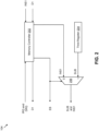
- FIG. 2 illustrates a schematic circuit diagram of the error control circuit 104 in accordance with an embodiment of the present disclosure.
- the error control circuit 104 may include a memory controller 202, a third register 204, and a multiplexer 206.
- the memory controller 202 may be coupled to the processor 102, the first memory 106, the second memory 108, the system controller 110, the logic gate 118, and the multiplexer 206.
- the memory controller 202 may include suitable circuitry that may be configured to perform one or more operations.
- the memory controller 202 may be configured to receive the instruction request IRQ from the processor 102. Based on the instruction request IRQ, the memory controller 202 may be configured to retrieve various instructions from the first memory 106 in a sequential manner.
- the memory controller 202 may be configured to initially retrieve the first instruction INS1 from the first memory 106. Further, the memory controller 202 may be configured to determine whether the first instruction INS1 is erroneous or error-free.
- the memory controller 202 may be further configured to generate the error bit EB. Based on the determination that the first instruction INS1 is erroneous, the error bit EB is asserted. Conversely, the error bit EB is de-asserted based on the determination that the first instruction INS1 is error-free. As it is assumed that the first instruction INS1 is erroneous, the error bit EB is asserted. Based on the assertion of the error bit EB, the substitute instruction SUB is provided to the processor 102 as the response to the instruction request IRQ. Further, the memory controller 202 may be configured to provide the asserted error bit EB to the system controller 110 and the logic gate 118. Based on the error bit EB, the execution of the first thread TH1 may be suspended or may remain unaltered.
- the memory controller 202 may be further configured to receive another instruction request from the processor 102 to retrieve various instructions of the second thread TH2 from the first memory 106. For each instruction of the second thread TH2, the memory controller 202 may operate in a similar manner as for the first instruction INS1. Further, after the execution of the first thread TH1 is suspended, the first thread TH1 is disabled, the erroneous first instruction INS1 is corrected, and the first thread TH1 is re-enabled.
- the re-enabled first thread TH1 may then be scheduled for execution at the processor 102 after the execution of the second thread TH2 is complete.
- the processor 102 may regenerate the instruction request IRQ and provide the instruction request IRQ to the memory controller 202.
- the memory controller 202 may again retrieve the first instruction INS1 from the first memory 106 and determine whether the first instruction INS1 is erroneous or error-free. As the first instruction INS1 is corrected, the memory controller 202 may generate the error bit EB in a de-asserted state and the first instruction INS1 is provided to the processor 102 for execution. In such a scenario, the execution of the first thread TH1 remains unaltered.
- the memory controller 202 may be further configured to receive the data request DRQ from the processor 102. Based on the data request DRQ, the memory controller 202 may be further configured to retrieve the first data D1 of the first data set DS1 from the second memory 108. The memory controller 202 may be further configured to determine whether the first data D1 is erroneous or error-free. As it is assumed that the first data D1 is erroneous, the memory controller 202 may be further configured to generate another error bit (such as the error bit EB) in an asserted state and provide the first data D1 to the processor 102. Based on the erroneous first data D1, the execution of the first thread TH1 may be suspended or may remain unaltered.
- error bit EB error bit
- the processor 102 may regenerate the instruction request IRQ and provide the instruction request IRQ to the memory controller 202. In such a scenario, as the first instruction INS1 and the first data D1 are corrected, the execution of the first instruction INS1 may be successful.
- the third register 204 may be coupled to the multiplexer 206.
- the third register 204 may be configured to store the substitute instruction SUB.
- the substitute instruction SUB may be stored in the third register 204 during the boot-up of the IC 100 by the core circuit.
- the multiplexer 206 may be coupled to the memory controller 202, the third register 204, and the processor 102.
- the multiplexer 206 may be configured to receive the first instruction INS1 and the error bit EB from the memory controller 202. Further, the multiplexer 206 may be configured to receive the substitute instruction SUB from the third register 204. Based on the error bit EB, the multiplexer 206 may be further configured to provide the first instruction INS1 or the substitute instruction SUB to the processor 102. Based on the assertion of the error bit EB, the multiplexer 206 may provide the substitute instruction SUB to the processor 102. Alternatively, based on the de-assertion of the error bit EB, the multiplexer 206 may provide the first instruction INS1 to the processor 102.
- the multiplexer 206 may receive the instruction and the associated error bit from the memory controller 202 and the substitute instruction SUB from the third register 204. Further, based on the received error bit, the multiplexer 206 may provide the retrieved instruction or the substitute instruction SUB to the processor 102.
- FIG. 2 illustrates that the error control circuit 104 includes a single register storing one substitute instruction
- the scope of the present disclosure is not limited to it.
- the error control circuit 104 may include various registers storing various substitute instructions, and various multiplexers for providing different substitute instructions to the processor 102 in place of the erroneous thread instructions.
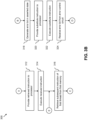
- FIGS. 3A-3D collectively, represents a flowchart 300 that illustrates a memory error management method in accordance with an embodiment of the present disclosure.
- the memory error management method may be implemented by the IC 100 to manage memory errors occurring in the first and second memories 106 and 108.
- the first memory 106 may store the first and second threads TH1 and TH2
- the second memory 108 may store the first and second data sets DS1 and DS2 associated with the first and second threads TH1 and TH2, respectively.
- the processor 102 may generate, when the first thread TH1 is scheduled for execution, the instruction request IRQ to retrieve the one or more instructions of the first thread TH1 ( e.g. , the first set of instructions).
- the error control circuit 104 may receive the instruction request IRQ from the processor 102.
- the error control circuit 104 may retrieve one instruction (e.g., the first instruction INS1) from the first memory 106 based on the instruction request IRQ.
- the error control circuit 104 may determine whether the retrieved instruction (e.g., the first instruction INS1) is erroneous or error-free. If at step 310, the error control circuit 104 determines that the retrieved instruction is error-free, step 312 is performed.
- the error control circuit 104 may provide the retrieved instruction (e.g., the first instruction INS1) to the processor 102.
- the processor 102 may execute the received instruction (e.g., the first instruction INS1).
- the execution of the first instruction INS1 may be successful or unsuccessful.
- the error control circuit 104 may retrieve a subsequent instruction of the first thread TH1 from the first memory 106. Step 310 is performed after step 316.
- step 318 is performed.
- the error control circuit 104 may generate the error bit EB in an asserted state.
- the error control circuit 104 may provide the substitute instruction SUB to the processor 102.
- the processor 102 may execute the substitute instruction SUB.
- the system controller 110 and the logic gate 118 may receive, from the error control circuit 104, the error bit EB that is indicative of the erroneous first instruction INS1.
- the system controller 110 or the first suspension control bit SC1 may determine whether the execution of the first thread TH1 is to be suspended. If at step 326, it is determined that the execution of the first thread TH1 is to remain unaltered, step 316 is performed. If at step 326, it is determined that the execution of the first thread TH1 is to be suspended, step 328 is performed.
- the thread scheduler 120 may generate the suspend request SRQ to suspend the execution of the first thread TH1.
- the suspend request SRQ may be generated based on the assertion of the first trigger bit TG1 generated by the system controller 110.
- the suspend request SRQ may be generated based on the assertion of the second trigger bit TG2 generated by the logic gate 118 ( e.g., the assertion of the first suspension control bit SC1 stored in the first register 112 and the de-assertion of the second suspension control bit SC2 stored in the second register 114).
- the thread scheduler 120 may provide the suspend request SRQ to the processor 102.
- the processor 102 may suspend the execution of the first thread TH1.
- the processor 102 may generate the acknowledgment ACK indicative of the successful suspension of the execution of the first thread TH1.
- the processor 102 may provide the acknowledgment ACK to the thread scheduler 120.
- the thread scheduler 120 may generate the thread switching signal TSW based on the acknowledgment ACK.
- the thread scheduler 120 may provide the thread switching signal TSW to the processor 102.
- the processor 102 may initiate the execution of the second thread TH2 based on the thread switching signal TSW.
- the thread scheduler 120 may disable the first thread TH1 based on the acknowledgment ACK.
- the system controller 110 may correct the erroneous instruction (e.g., the erroneous first instruction INS1).
- the system controller 110 generates the thread control bit TCT indicative of the successful correction of the erroneous first instruction INS1.
- the thread scheduler 120 receives the thread control bit TCT from the system controller 110.
- the thread scheduler 120 re-enables the first thread TH1 based on the thread control bit TCT. To re-enable the first thread TH1, the thread scheduler 120 modifies the context associated with the first thread TH1.
- the flowchart 300 describes the management of erroneous instruction (e.g., the first instruction INS1).
- the re-enabled first thread TH1 may then be scheduled for execution at the processor 102 after the execution of the second thread TH2 is complete.
- the first instruction INS1 is corrected, the first instruction INS1 is provided to the processor 102 for execution and the execution of the first thread TH1 remains unaltered.
- the execution of the first instruction INS1 may be successful or unsuccessful.
- the associated data of the first data set DS1 may be retrieved from the second memory 108 and it may be determined whether the retrieved data is erroneous or error-free.
- the retrieved data e.g., the first data D1
- the first data D1 is provided to the processor 102 and the execution of the first thread TH1 remains unaltered. If the retrieved data (e.g., the first data D1) is erroneous, the first data D1 is provided to the processor 102 and the execution of the first thread TH1 may be suspended in a similar manner as described above.
- the processor 102 may initiate the execution of a subsequent thread and the thread scheduler 120 may disable the first thread TH1 in a similar manner as described above. Further, after the first thread TH1 is disabled, the system controller 110 may correct the erroneous first data D1 and the thread scheduler 120 may re-enable the first thread TH1 based on the successful correction of the erroneous first data D1 in a similar manner as described above.
- the processor 102 may regenerate the instruction request IRQ and provide the instruction request IRQ to the error control circuit 104.
- the execution of the first instruction INS1 may be successful and the error control circuit 104 may retrieve a subsequent instruction of the first thread TH1 from the first memory 106.
- the entire IC may be reset or an IC subsystem that includes the processor may be reset.
- the reset of the IC subsystem or the entire IC takes up a significant amount of clock cycles.
- the significant turnaround time associated with the reset of the IC subsystem or the entire IC is undesirable for safety-critical applications (e.g., automotive applications).
- the operations of all the other threads that are being executed by the processor are disrupted by an error in one thread. As a result, the throughput of the processor significantly degrades.
- the replacement of the erroneous instruction (e.g., the first instruction INS1) with the substitute instruction SUB and the suspension of the execution of the erroneous thread (e.g., the first thread TH1) prevents the operational failure of the processor 102 due to memory errors.
- a need to reset the entire IC 100 or an IC subsystem (e.g., the processor 102) is reduced.
- the IC 100 may thus be implemented in the safety-critical applications.
- the execution of one thread is suspended, another thread is scheduled for execution at the processor 102.
- the operation of the processor 102 may not be halted due to the memory errors.
- the operations of other threads e.g., the second thread TH2
- the throughput of the processor 102 is significantly greater than that of processors that experience operational failures due to memory errors.
- An integrated circuit includes a memory that stores a thread and a processor that generates an instruction request to retrieve one or more instructions of the thread.
- the IC further includes an error control circuit that receives the instruction request from the processor and retrieves an instruction of the thread from the memory based on the instruction request. Further, the error control circuit determines whether the retrieved instruction is erroneous. Based on the determination that the retrieved instruction is erroneous, the error control circuit provides a substitute instruction to the processor as a response to the instruction request.
- the substitute instruction is included in an instruction set of the processor.
- the processor executes the received substitute instruction and suspends an execution of the thread.
- assert is used to mean placing a signal in an active state. For example, for an active-low signal, the signal is at a logic low state when asserted, and for an active-high signal, the signal is at a logic high state when asserted.
Landscapes
- Engineering & Computer Science (AREA)
- Theoretical Computer Science (AREA)
- Physics & Mathematics (AREA)
- General Engineering & Computer Science (AREA)
- General Physics & Mathematics (AREA)
- Human Computer Interaction (AREA)
- Quality & Reliability (AREA)
- Computer Security & Cryptography (AREA)
- Hardware Redundancy (AREA)
- Retry When Errors Occur (AREA)
Claims (14)
- Integrierte Schaltung, IC, (100), umfassend:einen ersten Speicher (106), der dazu ausgelegt ist, einen ersten Thread (TH1) zu speichern, wobei der erste Thread (TH1) einen Satz von Anweisungen umfasst;einen Prozessor (102), der dazu ausgelegt ist, eine Anweisungsanforderung (IRQ) zu erzeugen, um eine oder mehrere Anweisungen des Satzes von Anweisungen abzurufen; undeine Fehlersteuerschaltung (104), die mit dem ersten Speicher (106) und dem Prozessor (102) gekoppelt ist und ausgelegt ist zum:Empfangen der Anweisungsanforderung (IRQ) vom Prozessor (102) ;Abrufen einer ersten Anweisung (INS1) des Satzes von Anweisungen aus dem ersten Speicher (106) basierend auf der Anweisungsanforderung (IRQ);Bestimmen, ob die erste Anweisung (INS1) fehlerhaft ist; undBereitstellen, basierend auf der Bestimmung, dass die erste Anweisung (INS1) fehlerhaft ist, einer Ersatzanweisung (SUB) an den Prozessor (102) als eine Antwort auf die Anweisungsanforderung (IRQ), wobei die Ersatzanweisung (SUB) in einem Anweisungssatz des Prozessors (102) enthalten ist, wobei der Prozessor (102) ferner dazu ausgelegt ist, die empfangene Ersatzanweisung (SUB) auszuführen, und wobei, nach der Ausführung der Ersatzanweisung (SUB), der Prozessor (102) ferner dazu ausgelegt ist, eine Ausführung des ersten Threads (TH1) basierend auf der fehlerhaften ersten Anweisung (INS1) zu suspendieren, wobei die IC (100) ferner (i) einen Thread-Scheduler (120) und (ii) eine Systemsteuerung (110), die mit dem Thread-Scheduler (120) gekoppelt ist, umfasst,wobei die Systemsteuerung (110) dazu ausgelegt ist, die fehlerhafte erste Anweisung (INS1) zu korrigieren, nachdem der erste Thread (TH1) deaktiviert ist, und ein Thread-Steuerbit (TCT) zu erzeugen, das die erfolgreiche Korrektur der fehlerhaften ersten Anweisung (INS1) angibt,wobei der Thread-Scheduler (120) ferner dazu ausgelegt ist, das Thread-Steuerbit (TCT) von der Systemsteuerung (110) zu empfangen und den ersten Thread (TH1) wieder zu aktivieren,wobei das Wiederaktivieren des ersten Threads (TH1) einem Einschluss des ersten Threads (TH1) beim mit dem Prozessor (102) assoziierten Multithreading entspricht, undwobei zum Wiederaktivieren des ersten Threads (TH1) der Thread-Scheduler (120) ferner dazu ausgelegt ist, einen mit dem ersten Thread (TH1) assoziierten Kontext zu modifizieren.
- IC (100) nach Anspruch 1, wobei der Thread-Scheduler (120) mit dem Prozessor (102) gekoppelt ist und ausgelegt ist zum:Erzeugen, basierend auf der Suspendierung der Ausführung des ersten Threads (TH1), eines Thread-Umschaltsignals (TSW) zum Initiieren einer Ausführung eines zweiten Threads (TH2), der mit dem Prozessor (102) assoziiert ist, wobei der erste Speicher (106) ferner dazu ausgelegt ist, den zweiten Thread (TH2) zu speichern; undBereitstellen des Thread-Umschaltsignals (TSW) an den Prozessor (102), wobei der Prozessor (102) ferner dazu ausgelegt ist, die Ausführung des zweiten Threads (TH2) basierend auf dem Thread-Umschaltsignal (TSW) zu initiieren.
- IC (100) nach einem vorstehenden Anspruch, wobei der Thread-Scheduler (120) dazu ausgelegt ist, den ersten Thread (TH1) basierend auf der Suspendierung der Ausführung des ersten Threads (TH1) zu deaktivieren, wobei das Deaktivieren des ersten Threads (TH1) dem Ausschluss des ersten Threads (TH1) vom mit dem Prozessor (102) assoziierten Multithreading entspricht.
- IC (100) nach einem vorstehenden Anspruch, ferner umfassend einen zweiten Speicher (108), der mit der Fehlersteuerschaltung (104) gekoppelt ist,wobei der zweite Speicher (108) dazu ausgelegt ist, einen Datensatz (DS1) zu speichern, der mit dem ersten Thread (TH1) assoziiert ist,wobei, basierend auf dem Wiederaktivieren des ersten Threads (TH1), der Prozessor (102) ferner dazu ausgelegt ist, die erste Anweisung (INS1) von der Fehlersteuerschaltung (104) zu empfangen und die empfangene erste Anweisung (INS1) auszuführen,wobei die Fehlersteuerschaltung (104) ferner dazu ausgelegt ist, (i) eine Datenanforderung (DRQ) während der Ausführung der ersten Anweisung (INS1) vom Prozessor (102) zu empfangen, (ii) erste Daten (D1) des Datensatzes (DS1) aus dem zweiten Speicher (108) basierend auf der Datenanforderung (DRQ) abzurufen und (iii) zu bestimmen, ob die ersten Daten (D1) fehlerhaft sind, undwobei der Prozessor (102) ferner dazu ausgelegt ist, die Ausführung des ersten Threads (TH1) basierend auf den fehlerhaften ersten Daten (D1) zu suspendieren.
- IC (100) nach einem vorstehenden Anspruch, wobei der Thread-Scheduler (120) mit dem Prozessor gekoppelt ist und dazu ausgelegt ist, eine Suspendierungsanforderung (SRQ) basierend auf der fehlerhaften ersten Anweisung (INS1) zu erzeugen und die Suspendierungsanforderung (SRQ) dem Prozessor (102) bereitzustellen, wobei der Prozessor (102) die Ausführung des ersten Threads (TH1) als Reaktion auf die Suspendierungsanforderung (SRQ) suspendiert.
- IC (100) nach Anspruch 5, wobei die Fehlersteuerschaltung (104) ferner dazu ausgelegt ist, ein Fehlerbit (EB) zu erzeugen, wobei das Fehlerbit (EB) basierend auf der Bestimmung aktiv gesetzt wird, dass die erste Anweisung (INS1) fehlerhaft ist, und wobei die Suspendierungsanforderung (SRQ) basierend auf dem Fehlerbit (EB) erzeugt wird.
- IC (100) nach Anspruch 6, wobei die Systemsteuerung (110) mit der Fehlersteuerschaltung (104) gekoppelt ist und ausgelegt ist zum:Empfangen des Fehlerbits (EB) von der Fehlersteuerschaltung (104);Bestimmen, ob die Ausführung des ersten Threads (TH1) suspendiert werden soll, basierend auf der Aktivsetzung des Fehlerbits (EB);Erzeugen eines ersten Auslösebits (TG1), das angibt, ob die Ausführung des ersten Threads (TH1) suspendiert werden soll, wobei das erste Auslösebit (TG1) aktiv gesetzt wird, um anzugeben, dass die Ausführung des ersten Threads (TH1) suspendiert werden soll; undBereitstellen des ersten Auslösebits (TG1) an den Thread-Scheduler (120), wobei der Thread-Scheduler (120) die Suspendierungsanforderung (SRQ) basierend auf der Aktivsetzung des ersten Auslösebits (TG1) erzeugt.
- IC (100) nach einem der Ansprüche 6 oder 7, ferner umfassend ein Logikgatter (118), das mit der Fehlersteuerschaltung (104) und dem Thread-Scheduler (120) gekoppelt ist und ausgelegt ist zum:Empfangen des Fehlerbits (EB) von der Fehlersteuerschaltung (104);Empfangen eines Suspendierungssteuerbits (SC1, SC3), wobei das Suspendierungssteuerbit (SC1, SC3) aktiv gesetzt wird, um anzugeben, dass die Ausführung des ersten Threads (TH1) suspendiert werden soll, wenn der erste Thread (TH1) fehlerhaft ist;Erzeugen eines zweiten Auslösebits (TG2) basierend auf dem Fehlerbit (EB) und dem Suspendierungssteuerbit (SC1, SC3), wobei das zweite Auslösebit (TG2) basierend auf der Aktivsetzung sowohl des Fehlerbits (EB) als auch des Suspendierungssteuerbits (SC1, SC3) aktiv gesetzt wird, und wobei das zweite Auslösebit (TG2) basierend auf einer Inaktivsetzung von mindestens einem aus einer Gruppe, die aus dem Fehlerbit (EB) und dem Suspendierungssteuerbit (SC1, SC3) besteht, inaktiv gesetzt wird; undBereitstellen des zweiten Auslösebits (TG2) an den Thread-Scheduler (120), wobei der Thread-Scheduler (120) die Suspendierungsanforderung (SRQ) basierend auf der Aktivsetzung des zweiten Auslösebits (TG2) erzeugt.
- IC (100) nach Anspruch 8, ferner umfassend ein erstes Register (112), das mit dem Logikgatter (118) gekoppelt ist und dazu ausgelegt ist, das Suspendierungssteuerbit (SC1) zu speichern, wobei das Suspendierungssteuerbit (SC1) während eines Boot-Up der IC (100) im ersten Register (112) gespeichert wird.
- IC (100) nach einem vorstehenden Anspruch, wobei die Fehlersteuerschaltung (104) eine Speichersteuerung (202) umfasst, die mit dem ersten Speicher (106) und dem Prozessor (102) gekoppelt ist und ausgelegt ist zum:Empfangen der Anweisungsanforderung (IRQ) vom Prozessor (102) ;Abrufen der ersten Anweisung (INS1) aus dem ersten Speicher (106) basierend auf der Anweisungsanforderung (IRQ);Bestimmen, ob die erste Anweisung (INS1) fehlerhaft ist; undErzeugen eines Fehlerbits (EB), wobei das Fehlerbit (EB) basierend auf der Bestimmung aktiv gesetzt wird, dass die erste Anweisung (INS1) fehlerhaft ist.
- IC (100) nach Anspruch 10, wobei die Fehlersteuerschaltung (104) ferner einen Multiplexer (206) umfasst, der mit der Speichersteuerung (202) und dem Prozessor (102) gekoppelt ist und ausgelegt ist zum:Empfangen der ersten Anweisung (INS1) und des Fehlerbits (EB) von der Speichersteuerung (202);Empfangen der Ersatzanweisung (SUB); undBereitstellen, basierend auf dem Fehlerbit (EB), eines von einer Gruppe, die aus der ersten Anweisung (INS1) und der Ersatzanweisung (SUB) besteht, an den Prozessor (102), wobei, basierend auf der Aktivsetzung des Fehlerbits (EB), dem Prozessor (102) die Ersatzanweisung (SUB) bereitgestellt wird.
- IC (100) nach einem vorstehenden Anspruch, wobei die Fehlersteuerschaltung (104) ein zweites Register (114) umfasst, das dazu ausgelegt ist, die Ersatzanweisung (SUB) zu speichern, und wobei die Ersatzanweisung (SUB) während eines Boot-Up der IC (100) im zweiten Register gespeichert wird.
- IC (100) nach einem vorstehenden Anspruch, wobei die erste Anweisung (INS1) infolge eines Speicherfehlers im ersten Speicher (106) fehlerhaft ist.
- Speicherfehlerverwaltungsverfahren, umfassend:Speichern, durch einen ersten Speicher (106) einer integrierten Schaltung, IC, (100), eines ersten Threads (TH1), wobei der erste Thread (TH1) einen Satz von Anweisungen umfasst;Erzeugen, durch einen Prozessor (102) der IC (100), einer Anweisungsanforderung (IRQ), um eine oder mehrere Anweisungen des Satzes von Anweisungen abzurufen;Empfangen, durch eine Fehlersteuerschaltung (104) der IC (100), der Anweisungsanforderung (IRQ) vom Prozessor (102) ;Abrufen, durch die Fehlersteuerschaltung (104), einer ersten Anweisung (INS1) des Satzes von Anweisungen aus dem ersten Speicher (106) basierend auf der Anweisungsanforderung (IRQ);Bestimmen, durch die Fehlersteuerschaltung (104), ob die erste Anweisung (INS1) fehlerhaft ist;Bereitstellen, durch die Fehlersteuerschaltung (104), basierend auf der Bestimmung, dass die erste Anweisung (INS1) fehlerhaft ist, einer Ersatzanweisung (SUB) an den Prozessor (102) als eine Antwort auf die Anweisungsanforderung (IRQ), wobei die Ersatzanweisung (SUB) in einem Anweisungssatz des Prozessors (102) enthalten ist;Ausführen, durch den Prozessor (102), der Ersatzanweisung (SUB);Suspendieren, durch den Prozessor (102), nachdem die Ersatzanweisung (SUB) ausgeführt ist, einer Ausführung des ersten Threads (TH1) basierend auf der fehlerhaften ersten Anweisung (INS1);Korrigieren, durch die Systemsteuerung (110), der fehlerhaften ersten Anweisung (INS1), nachdem der erste Thread (TH1) deaktiviert ist, und Erzeugen, durch die Systemsteuerung (110), eines Thread-Steuerbits (TCT), das die erfolgreiche Korrektur der fehlerhaften ersten Anweisung (INS1) angibt;Empfangen, durch den Thread-Scheduler (120), des Thread-Steuerbits (TCT) von der Systemsteuerung (110) und Wiederaktivieren, durch den Thread-Scheduler (120), des ersten Threads (TH1), wobei das Wiederaktivieren des ersten Threads (TH1) einem Einschluss des ersten Threads (TH1) beim mit dem Prozessor (102) assoziierten Multithreading entspricht; undModifizieren, durch den Thread-Scheduler (120), eines mit dem ersten Thread (TH1) assoziierten Kontexts, um den ersten Thread (TH1) wieder zu aktivieren.
Applications Claiming Priority (1)
| Application Number | Priority Date | Filing Date | Title |
|---|---|---|---|
| US17/652,933 US12164781B2 (en) | 2022-03-01 | 2022-03-01 | System and method for managing memory errors in integrated circuits |
Publications (2)
| Publication Number | Publication Date |
|---|---|
| EP4239480A1 EP4239480A1 (de) | 2023-09-06 |
| EP4239480B1 true EP4239480B1 (de) | 2024-10-02 |
Family
ID=85384617
Family Applications (1)
| Application Number | Title | Priority Date | Filing Date |
|---|---|---|---|
| EP23158725.4A Active EP4239480B1 (de) | 2022-03-01 | 2023-02-27 | System und verfahren zur verwaltung von speicherfehlern in integrierten schaltungen |
Country Status (2)
| Country | Link |
|---|---|
| US (1) | US12164781B2 (de) |
| EP (1) | EP4239480B1 (de) |
Family Cites Families (7)
| Publication number | Priority date | Publication date | Assignee | Title |
|---|---|---|---|---|
| US4538265A (en) | 1983-03-24 | 1985-08-27 | International Business Machines Corporation | Method and apparatus for instruction parity error recovery |
| DE19964003A1 (de) * | 1999-12-30 | 2001-07-12 | Micronas Gmbh | Schaltungsanordnung und Verfahren zur Erzeugung und zum Auslesen von Ersatzdaten |
| US7278062B2 (en) | 2003-01-09 | 2007-10-02 | Freescale Semiconductor, Inc. | Method and apparatus for responding to access errors in a data processing system |
| US7849297B2 (en) | 2003-08-28 | 2010-12-07 | Mips Technologies, Inc. | Software emulation of directed exceptions in a multithreading processor |
| JP4334598B1 (ja) | 2008-04-16 | 2009-09-30 | 株式会社東芝 | 情報処理装置およびエラー訂正方法 |
| US10216521B2 (en) | 2017-06-20 | 2019-02-26 | Nvidia Corporation | Error mitigation for resilient algorithms |
| US10908987B1 (en) | 2019-03-28 | 2021-02-02 | Amazon Technologies, Inc. | Handling memory errors in computing systems |
-
2022
- 2022-03-01 US US17/652,933 patent/US12164781B2/en active Active
-
2023
- 2023-02-27 EP EP23158725.4A patent/EP4239480B1/de active Active
Also Published As
| Publication number | Publication date |
|---|---|
| EP4239480A1 (de) | 2023-09-06 |
| US20230280909A1 (en) | 2023-09-07 |
| US12164781B2 (en) | 2024-12-10 |
Similar Documents
| Publication | Publication Date | Title |
|---|---|---|
| US9891917B2 (en) | System and method to increase lockstep core availability | |
| CN109891393B (zh) | 使用检查器处理器的主处理器错误检测 | |
| US8095825B2 (en) | Error correction method with instruction level rollback | |
| US5537559A (en) | Exception handling circuit and method | |
| US8412981B2 (en) | Core sparing on multi-core platforms | |
| US8572441B2 (en) | Maximizing encodings of version control bits for memory corruption detection | |
| US8166338B2 (en) | Reliable exception handling in a computer system | |
| US8751736B2 (en) | Instructions to set and read memory version information | |
| US10817369B2 (en) | Apparatus and method for increasing resilience to faults | |
| US9348681B2 (en) | Apparatus and method for detecting fault of processor | |
| US20110185153A1 (en) | Simultaneous execution resumption of multiple processor cores after core state information dump to facilitate debugging via multi-core processor simulator using the state information | |
| US7721148B2 (en) | Method and apparatus for redirection of machine check interrupts in multithreaded systems | |
| US7861228B2 (en) | Variable delay instruction for implementation of temporal redundancy | |
| US7716537B2 (en) | Information processing apparatus and error correction method | |
| US10289332B2 (en) | Apparatus and method for increasing resilience to faults | |
| US10810039B2 (en) | Monitoring utilization of transactional processing resource | |
| JP6963552B2 (ja) | ブロックアトミック実行モデルを利用するプロセッサベースシステムにおける部分的に実行された命令ブロックのリプレイ | |
| US8769333B2 (en) | Application reliability and fault tolerant chip configurations | |
| US8516303B2 (en) | Arithmetic device for concurrently processing a plurality of threads | |
| US12164781B2 (en) | System and method for managing memory errors in integrated circuits | |
| CN108834427B (zh) | 处理向量指令 | |
| CN120523657A (zh) | 测试实现高速缓存功能的逻辑电路的计算机实现的方法 | |
| CN101027646A (zh) | 用于处理计算机系统上的计算机程序的方法 | |
| CN115576734B (zh) | 一种多核异构日志存储方法和系统 | |
| US20060195849A1 (en) | Method for synchronizing events, particularly for processors of fault-tolerant systems |
Legal Events
| Date | Code | Title | Description |
|---|---|---|---|
| PUAI | Public reference made under article 153(3) epc to a published international application that has entered the european phase |
Free format text: ORIGINAL CODE: 0009012 |
|
| STAA | Information on the status of an ep patent application or granted ep patent |
Free format text: STATUS: THE APPLICATION HAS BEEN PUBLISHED |
|
| AK | Designated contracting states |
Kind code of ref document: A1 Designated state(s): AL AT BE BG CH CY CZ DE DK EE ES FI FR GB GR HR HU IE IS IT LI LT LU LV MC ME MK MT NL NO PL PT RO RS SE SI SK SM TR |
|
| STAA | Information on the status of an ep patent application or granted ep patent |
Free format text: STATUS: REQUEST FOR EXAMINATION WAS MADE |
|
| 17P | Request for examination filed |
Effective date: 20240306 |
|
| RBV | Designated contracting states (corrected) |
Designated state(s): AL AT BE BG CH CY CZ DE DK EE ES FI FR GB GR HR HU IE IS IT LI LT LU LV MC ME MK MT NL NO PL PT RO RS SE SI SK SM TR |
|
| GRAP | Despatch of communication of intention to grant a patent |
Free format text: ORIGINAL CODE: EPIDOSNIGR1 |
|
| STAA | Information on the status of an ep patent application or granted ep patent |
Free format text: STATUS: GRANT OF PATENT IS INTENDED |
|
| INTG | Intention to grant announced |
Effective date: 20240517 |
|
| GRAS | Grant fee paid |
Free format text: ORIGINAL CODE: EPIDOSNIGR3 |
|
| GRAA | (expected) grant |
Free format text: ORIGINAL CODE: 0009210 |
|
| STAA | Information on the status of an ep patent application or granted ep patent |
Free format text: STATUS: THE PATENT HAS BEEN GRANTED |
|
| AK | Designated contracting states |
Kind code of ref document: B1 Designated state(s): AL AT BE BG CH CY CZ DE DK EE ES FI FR GB GR HR HU IE IS IT LI LT LU LV MC ME MK MT NL NO PL PT RO RS SE SI SK SM TR |
|
| REG | Reference to a national code |
Ref country code: GB Ref legal event code: FG4D |
|
| REG | Reference to a national code |
Ref country code: CH Ref legal event code: EP |
|
| REG | Reference to a national code |
Ref country code: IE Ref legal event code: FG4D |
|
| REG | Reference to a national code |
Ref country code: DE Ref legal event code: R096 Ref document number: 602023000630 Country of ref document: DE |
|
| REG | Reference to a national code |
Ref country code: LT Ref legal event code: MG9D |
|
| REG | Reference to a national code |
Ref country code: NL Ref legal event code: MP Effective date: 20241002 |
|
| REG | Reference to a national code |
Ref country code: AT Ref legal event code: MK05 Ref document number: 1728977 Country of ref document: AT Kind code of ref document: T Effective date: 20241002 |
|
| PG25 | Lapsed in a contracting state [announced via postgrant information from national office to epo] |
Ref country code: NL Free format text: LAPSE BECAUSE OF FAILURE TO SUBMIT A TRANSLATION OF THE DESCRIPTION OR TO PAY THE FEE WITHIN THE PRESCRIBED TIME-LIMIT Effective date: 20241002 |
|
| PG25 | Lapsed in a contracting state [announced via postgrant information from national office to epo] |
Ref country code: NL Free format text: LAPSE BECAUSE OF FAILURE TO SUBMIT A TRANSLATION OF THE DESCRIPTION OR TO PAY THE FEE WITHIN THE PRESCRIBED TIME-LIMIT Effective date: 20241002 |
|
| PG25 | Lapsed in a contracting state [announced via postgrant information from national office to epo] |
Ref country code: HR Free format text: LAPSE BECAUSE OF FAILURE TO SUBMIT A TRANSLATION OF THE DESCRIPTION OR TO PAY THE FEE WITHIN THE PRESCRIBED TIME-LIMIT Effective date: 20241002 Ref country code: IS Free format text: LAPSE BECAUSE OF FAILURE TO SUBMIT A TRANSLATION OF THE DESCRIPTION OR TO PAY THE FEE WITHIN THE PRESCRIBED TIME-LIMIT Effective date: 20250202 Ref country code: PT Free format text: LAPSE BECAUSE OF FAILURE TO SUBMIT A TRANSLATION OF THE DESCRIPTION OR TO PAY THE FEE WITHIN THE PRESCRIBED TIME-LIMIT Effective date: 20250203 |
|
| PG25 | Lapsed in a contracting state [announced via postgrant information from national office to epo] |
Ref country code: FI Free format text: LAPSE BECAUSE OF FAILURE TO SUBMIT A TRANSLATION OF THE DESCRIPTION OR TO PAY THE FEE WITHIN THE PRESCRIBED TIME-LIMIT Effective date: 20241002 |
|
| PG25 | Lapsed in a contracting state [announced via postgrant information from national office to epo] |
Ref country code: BG Free format text: LAPSE BECAUSE OF FAILURE TO SUBMIT A TRANSLATION OF THE DESCRIPTION OR TO PAY THE FEE WITHIN THE PRESCRIBED TIME-LIMIT Effective date: 20241002 |
|
| PG25 | Lapsed in a contracting state [announced via postgrant information from national office to epo] |
Ref country code: ES Free format text: LAPSE BECAUSE OF FAILURE TO SUBMIT A TRANSLATION OF THE DESCRIPTION OR TO PAY THE FEE WITHIN THE PRESCRIBED TIME-LIMIT Effective date: 20241002 |
|
| PG25 | Lapsed in a contracting state [announced via postgrant information from national office to epo] |
Ref country code: NO Free format text: LAPSE BECAUSE OF FAILURE TO SUBMIT A TRANSLATION OF THE DESCRIPTION OR TO PAY THE FEE WITHIN THE PRESCRIBED TIME-LIMIT Effective date: 20250102 |
|
| PG25 | Lapsed in a contracting state [announced via postgrant information from national office to epo] |
Ref country code: AT Free format text: LAPSE BECAUSE OF FAILURE TO SUBMIT A TRANSLATION OF THE DESCRIPTION OR TO PAY THE FEE WITHIN THE PRESCRIBED TIME-LIMIT Effective date: 20241002 Ref country code: GR Free format text: LAPSE BECAUSE OF FAILURE TO SUBMIT A TRANSLATION OF THE DESCRIPTION OR TO PAY THE FEE WITHIN THE PRESCRIBED TIME-LIMIT Effective date: 20250103 Ref country code: LV Free format text: LAPSE BECAUSE OF FAILURE TO SUBMIT A TRANSLATION OF THE DESCRIPTION OR TO PAY THE FEE WITHIN THE PRESCRIBED TIME-LIMIT Effective date: 20241002 |
|
| PG25 | Lapsed in a contracting state [announced via postgrant information from national office to epo] |
Ref country code: PL Free format text: LAPSE BECAUSE OF FAILURE TO SUBMIT A TRANSLATION OF THE DESCRIPTION OR TO PAY THE FEE WITHIN THE PRESCRIBED TIME-LIMIT Effective date: 20241002 Ref country code: CZ Free format text: LAPSE BECAUSE OF FAILURE TO SUBMIT A TRANSLATION OF THE DESCRIPTION OR TO PAY THE FEE WITHIN THE PRESCRIBED TIME-LIMIT Effective date: 20241002 |
|
| PG25 | Lapsed in a contracting state [announced via postgrant information from national office to epo] |
Ref country code: RS Free format text: LAPSE BECAUSE OF FAILURE TO SUBMIT A TRANSLATION OF THE DESCRIPTION OR TO PAY THE FEE WITHIN THE PRESCRIBED TIME-LIMIT Effective date: 20250102 |
|
| PG25 | Lapsed in a contracting state [announced via postgrant information from national office to epo] |
Ref country code: SM Free format text: LAPSE BECAUSE OF FAILURE TO SUBMIT A TRANSLATION OF THE DESCRIPTION OR TO PAY THE FEE WITHIN THE PRESCRIBED TIME-LIMIT Effective date: 20241002 |
|
| REG | Reference to a national code |
Ref country code: DE Ref legal event code: R097 Ref document number: 602023000630 Country of ref document: DE |
|
| PG25 | Lapsed in a contracting state [announced via postgrant information from national office to epo] |
Ref country code: DK Free format text: LAPSE BECAUSE OF FAILURE TO SUBMIT A TRANSLATION OF THE DESCRIPTION OR TO PAY THE FEE WITHIN THE PRESCRIBED TIME-LIMIT Effective date: 20241002 |
|
| PG25 | Lapsed in a contracting state [announced via postgrant information from national office to epo] |
Ref country code: EE Free format text: LAPSE BECAUSE OF FAILURE TO SUBMIT A TRANSLATION OF THE DESCRIPTION OR TO PAY THE FEE WITHIN THE PRESCRIBED TIME-LIMIT Effective date: 20241002 |
|
| PG25 | Lapsed in a contracting state [announced via postgrant information from national office to epo] |
Ref country code: RO Free format text: LAPSE BECAUSE OF FAILURE TO SUBMIT A TRANSLATION OF THE DESCRIPTION OR TO PAY THE FEE WITHIN THE PRESCRIBED TIME-LIMIT Effective date: 20241002 |
|
| PG25 | Lapsed in a contracting state [announced via postgrant information from national office to epo] |
Ref country code: SK Free format text: LAPSE BECAUSE OF FAILURE TO SUBMIT A TRANSLATION OF THE DESCRIPTION OR TO PAY THE FEE WITHIN THE PRESCRIBED TIME-LIMIT Effective date: 20241002 |
|
| PG25 | Lapsed in a contracting state [announced via postgrant information from national office to epo] |
Ref country code: IT Free format text: LAPSE BECAUSE OF FAILURE TO SUBMIT A TRANSLATION OF THE DESCRIPTION OR TO PAY THE FEE WITHIN THE PRESCRIBED TIME-LIMIT Effective date: 20241002 |
|
| P01 | Opt-out of the competence of the unified patent court (upc) registered |
Free format text: CASE NUMBER: APP_29984/2025 Effective date: 20250623 |
|
| PLBE | No opposition filed within time limit |
Free format text: ORIGINAL CODE: 0009261 |
|
| STAA | Information on the status of an ep patent application or granted ep patent |
Free format text: STATUS: NO OPPOSITION FILED WITHIN TIME LIMIT |
|
| PG25 | Lapsed in a contracting state [announced via postgrant information from national office to epo] |
Ref country code: SE Free format text: LAPSE BECAUSE OF FAILURE TO SUBMIT A TRANSLATION OF THE DESCRIPTION OR TO PAY THE FEE WITHIN THE PRESCRIBED TIME-LIMIT Effective date: 20241002 |
|
| 26N | No opposition filed |
Effective date: 20250703 |
|
| PG25 | Lapsed in a contracting state [announced via postgrant information from national office to epo] |
Ref country code: MC Free format text: LAPSE BECAUSE OF FAILURE TO SUBMIT A TRANSLATION OF THE DESCRIPTION OR TO PAY THE FEE WITHIN THE PRESCRIBED TIME-LIMIT Effective date: 20241002 |
|
| PG25 | Lapsed in a contracting state [announced via postgrant information from national office to epo] |
Ref country code: LU Free format text: LAPSE BECAUSE OF NON-PAYMENT OF DUE FEES Effective date: 20250227 |
|
| REG | Reference to a national code |
Ref country code: BE Ref legal event code: MM Effective date: 20250228 |
|
| PG25 | Lapsed in a contracting state [announced via postgrant information from national office to epo] |
Ref country code: FR Free format text: LAPSE BECAUSE OF NON-PAYMENT OF DUE FEES Effective date: 20250228 |
|
| PG25 | Lapsed in a contracting state [announced via postgrant information from national office to epo] |
Ref country code: BE Free format text: LAPSE BECAUSE OF NON-PAYMENT OF DUE FEES Effective date: 20250228 |
|
| PG25 | Lapsed in a contracting state [announced via postgrant information from national office to epo] |
Ref country code: IE Free format text: LAPSE BECAUSE OF NON-PAYMENT OF DUE FEES Effective date: 20250227 |
|
| PGFP | Annual fee paid to national office [announced via postgrant information from national office to epo] |
Ref country code: DE Payment date: 20260121 Year of fee payment: 4 |