EP4235777A2 - Multiple chip module with lid and stiffener ring - Google Patents
Multiple chip module with lid and stiffener ring Download PDFInfo
- Publication number
- EP4235777A2 EP4235777A2 EP23177407.6A EP23177407A EP4235777A2 EP 4235777 A2 EP4235777 A2 EP 4235777A2 EP 23177407 A EP23177407 A EP 23177407A EP 4235777 A2 EP4235777 A2 EP 4235777A2
- Authority
- EP
- European Patent Office
- Prior art keywords
- lid
- module
- accordance
- die
- module substrate
- Prior art date
- Legal status (The legal status is an assumption and is not a legal conclusion. Google has not performed a legal analysis and makes no representation as to the accuracy of the status listed.)
- Granted
Links
Images






Classifications
-
- H—ELECTRICITY
- H10—SEMICONDUCTOR DEVICES; ELECTRIC SOLID-STATE DEVICES NOT OTHERWISE PROVIDED FOR
- H10W—GENERIC PACKAGES, INTERCONNECTIONS, CONNECTORS OR OTHER CONSTRUCTIONAL DETAILS OF DEVICES COVERED BY CLASS H10
- H10W40/00—Arrangements for thermal protection or thermal control
- H10W40/20—Arrangements for cooling
- H10W40/22—Arrangements for cooling characterised by their shape, e.g. having conical or cylindrical projections
-
- H—ELECTRICITY
- H10—SEMICONDUCTOR DEVICES; ELECTRIC SOLID-STATE DEVICES NOT OTHERWISE PROVIDED FOR
- H10B—ELECTRONIC MEMORY DEVICES
- H10B80/00—Assemblies of multiple devices comprising at least one memory device covered by this subclass
-
- H—ELECTRICITY
- H10—SEMICONDUCTOR DEVICES; ELECTRIC SOLID-STATE DEVICES NOT OTHERWISE PROVIDED FOR
- H10W—GENERIC PACKAGES, INTERCONNECTIONS, CONNECTORS OR OTHER CONSTRUCTIONAL DETAILS OF DEVICES COVERED BY CLASS H10
- H10W76/00—Containers; Fillings or auxiliary members therefor; Seals
- H10W76/60—Seals
-
- H—ELECTRICITY
- H10—SEMICONDUCTOR DEVICES; ELECTRIC SOLID-STATE DEVICES NOT OTHERWISE PROVIDED FOR
- H10D—INORGANIC ELECTRIC SEMICONDUCTOR DEVICES
- H10D80/00—Assemblies of multiple devices comprising at least one device covered by this subclass
- H10D80/30—Assemblies of multiple devices comprising at least one device covered by this subclass the at least one device being covered by groups H10D84/00 - H10D86/00, e.g. assemblies comprising integrated circuit processor chips
-
- H—ELECTRICITY
- H10—SEMICONDUCTOR DEVICES; ELECTRIC SOLID-STATE DEVICES NOT OTHERWISE PROVIDED FOR
- H10W—GENERIC PACKAGES, INTERCONNECTIONS, CONNECTORS OR OTHER CONSTRUCTIONAL DETAILS OF DEVICES COVERED BY CLASS H10
- H10W40/00—Arrangements for thermal protection or thermal control
- H10W40/70—Fillings or auxiliary members in containers or in encapsulations for thermal protection or control
-
- H—ELECTRICITY
- H10—SEMICONDUCTOR DEVICES; ELECTRIC SOLID-STATE DEVICES NOT OTHERWISE PROVIDED FOR
- H10W—GENERIC PACKAGES, INTERCONNECTIONS, CONNECTORS OR OTHER CONSTRUCTIONAL DETAILS OF DEVICES COVERED BY CLASS H10
- H10W42/00—Arrangements for protection of devices
- H10W42/121—Arrangements for protection of devices protecting against mechanical damage
-
- H—ELECTRICITY
- H10—SEMICONDUCTOR DEVICES; ELECTRIC SOLID-STATE DEVICES NOT OTHERWISE PROVIDED FOR
- H10W—GENERIC PACKAGES, INTERCONNECTIONS, CONNECTORS OR OTHER CONSTRUCTIONAL DETAILS OF DEVICES COVERED BY CLASS H10
- H10W74/00—Encapsulations, e.g. protective coatings
- H10W74/10—Encapsulations, e.g. protective coatings characterised by their shape or disposition
- H10W74/131—Encapsulations, e.g. protective coatings characterised by their shape or disposition the semiconductor body being only partially enclosed
- H10W74/141—Encapsulations, e.g. protective coatings characterised by their shape or disposition the semiconductor body being only partially enclosed the encapsulations being on at least the sidewalls of the semiconductor body
-
- H—ELECTRICITY
- H10—SEMICONDUCTOR DEVICES; ELECTRIC SOLID-STATE DEVICES NOT OTHERWISE PROVIDED FOR
- H10W—GENERIC PACKAGES, INTERCONNECTIONS, CONNECTORS OR OTHER CONSTRUCTIONAL DETAILS OF DEVICES COVERED BY CLASS H10
- H10W76/00—Containers; Fillings or auxiliary members therefor; Seals
- H10W76/10—Containers or parts thereof
- H10W76/12—Containers or parts thereof characterised by their shape
-
- H—ELECTRICITY
- H10—SEMICONDUCTOR DEVICES; ELECTRIC SOLID-STATE DEVICES NOT OTHERWISE PROVIDED FOR
- H10W—GENERIC PACKAGES, INTERCONNECTIONS, CONNECTORS OR OTHER CONSTRUCTIONAL DETAILS OF DEVICES COVERED BY CLASS H10
- H10W76/00—Containers; Fillings or auxiliary members therefor; Seals
- H10W76/10—Containers or parts thereof
- H10W76/12—Containers or parts thereof characterised by their shape
- H10W76/15—Containers comprising an insulating or insulated base
-
- H—ELECTRICITY
- H10—SEMICONDUCTOR DEVICES; ELECTRIC SOLID-STATE DEVICES NOT OTHERWISE PROVIDED FOR
- H10W—GENERIC PACKAGES, INTERCONNECTIONS, CONNECTORS OR OTHER CONSTRUCTIONAL DETAILS OF DEVICES COVERED BY CLASS H10
- H10W76/00—Containers; Fillings or auxiliary members therefor; Seals
- H10W76/10—Containers or parts thereof
- H10W76/17—Containers or parts thereof characterised by their materials
-
- H—ELECTRICITY
- H10—SEMICONDUCTOR DEVICES; ELECTRIC SOLID-STATE DEVICES NOT OTHERWISE PROVIDED FOR
- H10W—GENERIC PACKAGES, INTERCONNECTIONS, CONNECTORS OR OTHER CONSTRUCTIONAL DETAILS OF DEVICES COVERED BY CLASS H10
- H10W76/00—Containers; Fillings or auxiliary members therefor; Seals
- H10W76/40—Fillings or auxiliary members in containers, e.g. centering rings
-
- H—ELECTRICITY
- H10—SEMICONDUCTOR DEVICES; ELECTRIC SOLID-STATE DEVICES NOT OTHERWISE PROVIDED FOR
- H10W—GENERIC PACKAGES, INTERCONNECTIONS, CONNECTORS OR OTHER CONSTRUCTIONAL DETAILS OF DEVICES COVERED BY CLASS H10
- H10W76/00—Containers; Fillings or auxiliary members therefor; Seals
- H10W76/40—Fillings or auxiliary members in containers, e.g. centering rings
- H10W76/42—Fillings
- H10W76/47—Solid or gel fillings
-
- H—ELECTRICITY
- H10—SEMICONDUCTOR DEVICES; ELECTRIC SOLID-STATE DEVICES NOT OTHERWISE PROVIDED FOR
- H10W—GENERIC PACKAGES, INTERCONNECTIONS, CONNECTORS OR OTHER CONSTRUCTIONAL DETAILS OF DEVICES COVERED BY CLASS H10
- H10W90/00—Package configurations
-
- H—ELECTRICITY
- H10—SEMICONDUCTOR DEVICES; ELECTRIC SOLID-STATE DEVICES NOT OTHERWISE PROVIDED FOR
- H10W—GENERIC PACKAGES, INTERCONNECTIONS, CONNECTORS OR OTHER CONSTRUCTIONAL DETAILS OF DEVICES COVERED BY CLASS H10
- H10W72/00—Interconnections or connectors in packages
- H10W72/071—Connecting or disconnecting
- H10W72/072—Connecting or disconnecting of bump connectors
-
- H—ELECTRICITY
- H10—SEMICONDUCTOR DEVICES; ELECTRIC SOLID-STATE DEVICES NOT OTHERWISE PROVIDED FOR
- H10W—GENERIC PACKAGES, INTERCONNECTIONS, CONNECTORS OR OTHER CONSTRUCTIONAL DETAILS OF DEVICES COVERED BY CLASS H10
- H10W72/00—Interconnections or connectors in packages
- H10W72/071—Connecting or disconnecting
- H10W72/073—Connecting or disconnecting of die-attach connectors
-
- H—ELECTRICITY
- H10—SEMICONDUCTOR DEVICES; ELECTRIC SOLID-STATE DEVICES NOT OTHERWISE PROVIDED FOR
- H10W—GENERIC PACKAGES, INTERCONNECTIONS, CONNECTORS OR OTHER CONSTRUCTIONAL DETAILS OF DEVICES COVERED BY CLASS H10
- H10W72/00—Interconnections or connectors in packages
- H10W72/20—Bump connectors, e.g. solder bumps or copper pillars; Dummy bumps; Thermal bumps
- H10W72/251—Materials
- H10W72/252—Materials comprising solid metals or solid metalloids, e.g. PbSn, Ag or Cu
-
- H—ELECTRICITY
- H10—SEMICONDUCTOR DEVICES; ELECTRIC SOLID-STATE DEVICES NOT OTHERWISE PROVIDED FOR
- H10W—GENERIC PACKAGES, INTERCONNECTIONS, CONNECTORS OR OTHER CONSTRUCTIONAL DETAILS OF DEVICES COVERED BY CLASS H10
- H10W72/00—Interconnections or connectors in packages
- H10W72/851—Dispositions of multiple connectors or interconnections
- H10W72/874—On different surfaces
- H10W72/877—Bump connectors and die-attach connectors
-
- H—ELECTRICITY
- H10—SEMICONDUCTOR DEVICES; ELECTRIC SOLID-STATE DEVICES NOT OTHERWISE PROVIDED FOR
- H10W—GENERIC PACKAGES, INTERCONNECTIONS, CONNECTORS OR OTHER CONSTRUCTIONAL DETAILS OF DEVICES COVERED BY CLASS H10
- H10W72/00—Interconnections or connectors in packages
- H10W72/90—Bond pads, in general
- H10W72/931—Shapes of bond pads
-
- H—ELECTRICITY
- H10—SEMICONDUCTOR DEVICES; ELECTRIC SOLID-STATE DEVICES NOT OTHERWISE PROVIDED FOR
- H10W—GENERIC PACKAGES, INTERCONNECTIONS, CONNECTORS OR OTHER CONSTRUCTIONAL DETAILS OF DEVICES COVERED BY CLASS H10
- H10W74/00—Encapsulations, e.g. protective coatings
- H10W74/10—Encapsulations, e.g. protective coatings characterised by their shape or disposition
- H10W74/15—Encapsulations, e.g. protective coatings characterised by their shape or disposition on active surfaces of flip-chip devices, e.g. underfills
-
- H—ELECTRICITY
- H10—SEMICONDUCTOR DEVICES; ELECTRIC SOLID-STATE DEVICES NOT OTHERWISE PROVIDED FOR
- H10W—GENERIC PACKAGES, INTERCONNECTIONS, CONNECTORS OR OTHER CONSTRUCTIONAL DETAILS OF DEVICES COVERED BY CLASS H10
- H10W76/00—Containers; Fillings or auxiliary members therefor; Seals
- H10W76/60—Seals
- H10W76/67—Seals characterised by their materials
-
- H—ELECTRICITY
- H10—SEMICONDUCTOR DEVICES; ELECTRIC SOLID-STATE DEVICES NOT OTHERWISE PROVIDED FOR
- H10W—GENERIC PACKAGES, INTERCONNECTIONS, CONNECTORS OR OTHER CONSTRUCTIONAL DETAILS OF DEVICES COVERED BY CLASS H10
- H10W90/00—Package configurations
- H10W90/701—Package configurations characterised by the relative positions of pads or connectors relative to package parts
- H10W90/721—Package configurations characterised by the relative positions of pads or connectors relative to package parts of bump connectors
- H10W90/724—Package configurations characterised by the relative positions of pads or connectors relative to package parts of bump connectors between a chip and a stacked insulating package substrate, interposer or RDL
-
- H—ELECTRICITY
- H10—SEMICONDUCTOR DEVICES; ELECTRIC SOLID-STATE DEVICES NOT OTHERWISE PROVIDED FOR
- H10W—GENERIC PACKAGES, INTERCONNECTIONS, CONNECTORS OR OTHER CONSTRUCTIONAL DETAILS OF DEVICES COVERED BY CLASS H10
- H10W90/00—Package configurations
- H10W90/701—Package configurations characterised by the relative positions of pads or connectors relative to package parts
- H10W90/731—Package configurations characterised by the relative positions of pads or connectors relative to package parts of die-attach connectors
- H10W90/734—Package configurations characterised by the relative positions of pads or connectors relative to package parts of die-attach connectors between a chip and a stacked insulating package substrate, interposer or RDL
-
- H—ELECTRICITY
- H10—SEMICONDUCTOR DEVICES; ELECTRIC SOLID-STATE DEVICES NOT OTHERWISE PROVIDED FOR
- H10W—GENERIC PACKAGES, INTERCONNECTIONS, CONNECTORS OR OTHER CONSTRUCTIONAL DETAILS OF DEVICES COVERED BY CLASS H10
- H10W90/00—Package configurations
- H10W90/701—Package configurations characterised by the relative positions of pads or connectors relative to package parts
- H10W90/731—Package configurations characterised by the relative positions of pads or connectors relative to package parts of die-attach connectors
- H10W90/736—Package configurations characterised by the relative positions of pads or connectors relative to package parts of die-attach connectors between a chip and a stacked lead frame, conducting package substrate or heat sink
Definitions
- Embodiments described herein relate to multiple chip modules, and in particular to lids thereof.
- Lids are widely used in multiple chip modules (MCMs) for a variety of reasons, such as to provide mechanical integrity, hermetic sealing from environment, and thermal performance.
- MCMs multiple chip modules
- one or more components are surface mounted onto a module substrate, and then optionally underfilled. A lid is then secured onto the module substrate and over the component(s).
- Embodiments describe multiple chip module (MCM) structures in which a combination of lid and stiffener structure is made to obtain the mechanical integrity and thermal benefits of a lid, and reduced warpage provided by the stiffener structure.
- the stiffener structure may reduce warpage potentially caused by mismatch of the coefficient of thermal expansion (CTE) of the lid and the rest of the MCM.
- Various lid designs are described which can further mitigate stress and warpage including trench designs to increase the volume ratio of the stiffener structure to lid, multiple piece lids, and hybrid lids.
- lids can provide mechanical integrity to an MCM
- lids can also induce large stress and high warpage in an MCM and induce mechanical failures.
- lids formed of copper may have a comparatively high coefficient of thermal expansion (CTE) relative to other module features. This can result in thermal expansion and induce stress and warpage in the MCM components (e.g. packages) when the lid is strongly coupled with the rest of the module.
- CTE coefficient of thermal expansion
- mold cracks can generate between overmolded side-by-side dies, which can be exacerbated by stress induced by a lid.
- various combinations of lids and stiffener structures are provided to balance the ability of the lid to provide mechanical integrity of the module while not inducing mechanical failure.
- the lid can include a trenched design.
- the trenched designs may include sufficient lid volume on top of the module components to retain sufficient thermal performance, while volume of the lid is reduced at connection areas to further reduce stress and warpage caused by the lid.
- a reduction of volume of the lid can correspond to an increase in volume of a stiffener structure, which increases the volume ratio of the stiffener structure to lid. This can further provide feasibility of selecting the stiffener structure material(s) to reduce the stress and warpage in the MCM.
- the stiffener structure (e.g. ring) can be fully or partially formed of a low CTE material.
- an increase of the stiffener structure to lid volume ratio (e.g. due to trenched lid design) facilitates the ability to reduce the effective CTE of the lid-stiffener combination by selecting a stiffener material with a lower CTE than the lid.
- a reduction of effective CTE of the lid-stiffener structure in turn can reduce stress and warpage issues of the MCM.
- a low CTE stiffener material can be a nickel-iron alloy (FeNi36), iron-nickel-cobalt alloy (sold under the trademark KOVAR, trademark of CRS Holdings, Inc., Delaware), iron-nickel alloy (Alloy42), stainless steels (SUS410, SUS430), etc. while the lid is formed of a higher CTE material such as copper.
- multiple piece lid designs are described.
- the multiple piece lid designs may reduce the coupling effect of the lid to the rest of the module, and further reduce stress caused by the lid. This may include a reduction of die-to-die molding compound stress, and module warpage.
- the multiple piece lid design incorporates different lid materials to meet different mechanical and thermal requirements of the MCMs.
- Hybrid lid designs are also described in which lids of different materials are bonded together or embedded, one within the other. By combining different materials, the effective CTE and stiffness of the lid can be tuned to match the target mechanical and thermal performance.
- the terms “above”, “over”, “to”, “between”, “spanning” and “on” as used herein may refer to a relative position of one layer with respect to other layers.
- One layer “above”, “over”, “spanning” or “on” another layer or bonded “to” or in “contact” with another layer may be directly in contact with the other layer or may have one or more intervening layers.
- One layer “between” layers may be directly in contact with the layers or may have one or more intervening layers.
- the MCM 150 includes a module substate 100 including a top side 102 and bottom side 104.
- a plurality of first components 120 can be mounted on the top side 102 of the module substrate 100.
- First components 120 may be active or passive devices, and may be chips or packages.
- first components 120 may be memory packages, such as dynamic random-access memory (DRAM) including one or more dies, which can be stacked dies, or side-by-side.
- DRAM dynamic random-access memory
- first components are chip scale packages.
- First components 120 can additionally be different types of components, and need not be identical.
- a second component 130 can also be mounted on the top side 102 of the module substrate 100.
- a second component 130 is a package that includes a plurality (e.g. two or more) of side-by-side dies.
- second component 130 may include a plurality of side-by-side logic, or system on chip dies.
- first components 120 and second component 130 are surface mounted onto the module substate 100 using any suitable technique such as solder bumps 160, with optional underfill 162 (e.g. epoxy).
- the second component 130 is a package that includes a plurality of side-by-side dies 132 incapsulated in a molding compound 134. As shown, the space 133 laterally between the dies 132 may be filled with molding compound 134. It has been observed this can be a high stress location within the MCM due to close proximity of a variety of materials and MCM structures.
- a thermal interface material (TIM) 170 can be located on top sides of the first components 120 and second component 130 in order to secure to the lid 300.
- TIM 170 may be applied using any suitable technique such as dispensing or tape.
- Exemplary TIM 170 materials include, but are not limited to, thermal grease, solder, metal filled polymer matrix, etc.
- the lid 300 can be bonded to an intermediate stiffener structure 200 (also referred to as a stiffener ring), which in turn is bonded to the module substrate 100.
- the stiffener structure 200 and lid 300 can be bonded using an adhesive material.
- adhesive can be dispensed onto the module substrate 100 at the connection areas (e.g. outer connection area 180 and inner connection area 182), followed by mounting the stiffener structure 200.
- Exemplary adhesive materials include glass paste, epoxies, urethane, polyurethane, silicone elastomers, etc.
- the lid 300 can similarly be bonded to the stiffener structure 200 after mounting the stiffener structure on the module substrate 100, or before.
- the lid 300 may include a roof 330, outer (periphery) walls 310 and optionally inner walls 320.
- the bottom surface 302 of the roof may be bonded to the TIM 170 on top of the second component 130 and first components 120. Contour of the bottom surface 302 (thickness of the roof 330) can be adjusted to evenly mate with the TIM 170 for the various first components 120 and second component 130.
- the outer walls 310 and inner walls 320 can extend from the roof 330 (e.g. protrude from the bottom surface) to form one or more cavities 305 which accommodate the second component 130 and first components 120.
- the stiffener structure 200 is shaped to mate with the outer walls 310 and inner walls 320 of the lid 300.
- the stiffener structure 200 can include outer support (walls) 210 and inner support 220 (walls).
- Outer support 210 and inner support 220 may be integrally formed of the same material.
- outer support 210 and inner support 220 can be formed of different materials with different CTE.
- the mating surfaces between the stiffener structure 200 and lid 300 may have a same surface area.
- a plurality of module solder bumps 190 may optionally be applied to the bottom side 104 of the module substrate 100 for further integration.
- various combinations of lids and stiffener structures are provided to balance the ability of the lid to provide mechanical integrity to the module while not inducing mechanical failure.
- various combinations of trenched lid designs, ratios of stiffener structure to lid volume, multiple piece lid designs, and combinations of materials with different CTE are described.
- the MCM 150 may include a module substrate 100, a first component 120 on the top side 102 of the module substrate and a second component 130 on the top side 102 of the module substrate.
- a stiffener structure 200 is mounted on the top side 102 of the module substrate and a lid 300 is mounted on the stiffener structure 200 and covering both the first component 120 and the second component 130.
- the stiffener structure 200 may be joined to the lid 300 within a trench 315 formed in a roof 330 of the lid.
- the stiffener structure 200 can include either or both of an outer support 210 and an inner support 220.
- FIG. 3 is a schematic cross-sectional side view illustration of a trenched design of a lid on an outer support 210 in accordance with an embodiment.
- a trench 315 is formed in the bottom surface 302 of the roof 330 of the lid 300.
- Each trench 315 may include one or more trench edges (sidewalls) 331 in the roof 330.
- a thickness of the roof 330 in the trench 315 area is less than a thickness of the roof 330 where the lid 300 is connected to the second component 130 with TIM 170, and where the lid 300 is connected to the first components 120 with TIM.
- the trench 315 reduces the volume of the lid 300 at the connection area.
- the trench 315 is formed at the outer (periphery) connection area 180 where the trench is joined with the outer support (walls) 210 of the stiffener structure 200.
- the trench does not include outer sidewalls (trench edge).
- the outer support 210 is joined to the lid 300 within the trench 315.
- the lid 300 may additionally include an inner wall 320 joined to an inner support 220 of the stiffener structure 200.
- FIG. 4 is a schematic cross-sectional side view illustration of a partial trenched design of a lid on an inner support in accordance with an embodiment.
- the inner support 220 is joined to the lid 300 within the trench 315.
- the lid 300 includes an outer wall 310 joined to the outer support 210.
- the inner support 220 is taller than the outer support 210.
- FIG. 5 is a schematic cross-sectional side view illustration of a partial trenched design of a lid on an outer support in accordance with an embodiment.
- the outer support 210 is joined to the lid 300 within the trench.
- the lid 300 additionally includes an inner wall 320 joined to the inner support 220.
- the outer support 210 is taller than the inner support 220.
- the inner wall 320 extends from the trench 315.
- the lid 300 can include both outer walls 310 and inner walls 320 extending from a trench 315.
- FIG. 6 is a schematic cross-sectional side view illustration of a partial trenched design of a lid on both an inner and outer support in accordance with an embodiment.
- FIG. 6 is similar to the embodiment illustrated in FIG. 3 with the addition of the inner support 220 also j oined to the lid within a trench 315, which may be the same trench or a separate trench than the trench 315 where the outer support 210 is joined to the lid.
- FIG. 7 is a schematic cross-sectional side view illustration of a partial trenched design of a lid on an inner or outer support in accordance with an embodiment. As shown, FIG. 7 combines features of FIGS. 4-6 to show a variety of configurations are possible, where portions of the inner support 220 and outer support 210 can have different heights, and outer wall 310 and inner wall 320 can be discontinuous.
- the trenched lid designs in accordance with embodiments can reduce the volume of lid at the connection areas to reduce stress and warpage caused by the lid. Furthermore, the reduction of volume of the lid can correspond to an increase in volume (height) of a stiffener structure, which increases the volume ratio of the stiffener structure to lid. In the illustrated embodiments, the ratio of stiffener structure to lid is greater than 1, meaning the stiffener structure can be taller than a thickness of the trenched roof of the lid.
- the stiffener structure can be fully or partially formed of a low CTE material.
- a low CTE stiffener material can be a nickel-iron alloy (FeNi36), iron-nickel-cobalt alloy (sold under the trademark KOVAR, trademark of CRS Holdings, Inc., Delaware), iron-nickel alloy (Alloy42), stainless steels (SUS410, SUS430), etc. while the lid is formed of a higher CTE material such as copper.
- the stiffener structure can also be formed of different materials (different chemical composition, or alloy ratios) to tune stress and warpage.
- FIG. 8 is a schematic cross-sectional side view illustration of a stiffener structure formed of adjacent materials with different coefficients of thermal expansion in accordance with an embodiment.
- the outer support 210 and the inner support 220 can be formed of different materials 221, 223 with a different CTE.
- different areas of the outer support 210 and inner support 220 can be formed of different materials 221, 223 to locally tune stress and warpage.
- FIG. 9 is a schematic cross-sectional side view illustration of a stiffener structure formed of stacked materials 221, 223 with different coefficients of thermal expansion in accordance with an embodiment. Furthermore, the relative thickness of the stacked materials 221, 223 can be different in different areas of the outer support 210 and inner support 220.
- the lids in accordance with embodiments may also have a plurality of physically separate pieces. Such multiple piece lid designs may reduce the coupling effect of the lid to the rest of the module, and further reduce stress caused by the lid. This may include a reduction of die-to-die molding compound stress, and module warpage.
- the lid 300 may include a plurality of physically separate roofs 330A, 330B, 330C bonded to the stiffener structure 200.
- the roofs 330A, 330B, 330C may additionally have a trench design including trenches 315.
- trenches 315 may be formed along the sides of the roofs 330A, 330B, 330C such that a pair of roofs are bonded to each inner support 220, and a single roof is bonded to each outer support 210.
- Each lid may be anchored to its surrounding inner support 220, and/or outer support 210.
- the lid may further include a component recess 335 which mates with a component (e.g. second component 130) edges.
- the component recess 335 may promote coverage of the TIM 170 with the component edges and reduce TIM peeling stress.
- FIGS. 11A-11B schematic top view and cross-sectional side view illustrations are provided of a multiple piece lid in accordance with embodiments.
- FIGS. 11A-11B differ from the embodiment of FIGS. 10A-10B in that the trenches 225 are formed within the inner support 220 and/or outer support 210 as opposed to the roofs of the lid. Similarly, trenches 225 may include trench edges 227.
- the inner supports 220 include trenches 225 to accommodate a roof 330A of lid 300.
- the physically separate roofs 330A, 330B, 330C of FIG. 11A-11B may have different thicknesses to manage stress and warpage.
- FIGS. 12A-12C schematic cross-sectional side view and top view illustrations are provided of multiple piece lids in accordance with an embodiment. It is to be appreciated that while illustrated and described separately, that the multiple piece lid embodiments of FIGS. 12A-12C are combinable with the multiple piece lid embodiments of FIGS. 10A-11B , as well as other embodiments described herein.
- the multiple piece lid 300 may include a first lid piece 300A spanning over a first die 132 in the second component 130 and a second lid piece 300B spanning over a second die 132 in the second component 130. Multiple lid pieces may be included 300A, 300B, 300C, 300D, etc.
- the molding compound 134 may fill a space 133 laterally between the first die 132 and the second die 132, which can correspond to a high stress region.
- a gap 325 may be located between the first lid piece 300A and the second lid piece 300B. In the illustrated embodiment the gap 325 is directly above the space 133 that is laterally between the first die 132 and the second die 132 of the component 130, which may be filled with the molding compound 134.
- the gap 325 may further reduce the coupling effect of the lid to the rest of the module, and further reduce stress caused by the lid.
- the separate lid pieces 300A, 300B, etc. may be formed of different materials 321, 323. Use of different lid material may be tuned to meet different mechanical and thermal requirements of the microelectronic module.
- the gap 325 may optionally be filled as shown in FIGS. 13A-13B with a fill material 400.
- the fill material may be a solder, adhesive, etc.
- a hybrid lid 300 design can include different materials bonded together or embedded, one within the other. By combining different materials, the effective CTE and stiffness of the lid can be tuned to match the target mechanical and thermal performance.
- a lid 300 may include a first lid pattern 500 bonded to a roof 330 of a main lid structure, wherein the first lid pattern 500 has a different CTE than the main lid structure.
- the main lid structure may be similar to the previously described lids 300 with the addition of a female pattern 360 into which the first lid pattern 500 is secured.
- the first lid pattern 500 may include a variety of features, which may optionally include an inner rib 520 and outer (peripheral) contour 510.
- the first lid pattern 500 may be located at high stress regions, such as at connection areas (180, 182) and over the space between side-by-side dies.
- the inner rib 520 is directly over the space 133 between adjacent dies 132.
- one or more local openings may be formed in any of the lid structures to reduce stress and warpage.
- FIGS. 15A-15C illustrate an exemplary implementation of such a local opening 326. As shown, FIGS. 15A-15C are similar to the lid design previously illustrated and described with regard to FIGS. 2A-2C , though embodiments are not so limited.
- the one or more local openings 326 may be located directly above (over) the space 133 laterally between dies 132.
- the one or more local opening 326 may completely or partially overlap the space 133.
- One or more local openings can also be located over other regions to mitigate stress.
- the one or more local openings 326 are formed completely through the roof 330 of the lid from the top side 304 to the bottom surface 302 of the roof 330.
- FIG. 16A is a schematic cross-sectional side view illustration of a lid design on an inner and outer support with the outer connection area 180 overhanging the module substrate 100 in accordance with an embodiment.
- FIG. 16B is a schematic cross-sectional side view illustration of a lid design on an outer support with the outer connection area 180 overhanging the module substrate 100 in accordance with an embodiment.
- the particular embodiments illustrated in FIGS. 16A-16B are similar to those previously illustrated and described with regard to FIGS.
- overhanging designs are combinable with any of the stiffener structure 200 inner and outer supports 220, 210, and lid 300 combinations with corresponding inner walls 320 and outer walls 310.
- the overhanging designs are also compatible with the multiple piece lid structures described herein.
- the overhanging lid designs in accordance with embodiments may overhang one or more, or all, peripheral (lateral) edges 106 of the module substrate 100.
- one or more peripheral edges 216 of the stiffener structure 200 and/or peripheral edges 316 of the lid(s) 300 corresponding to the outer connection areas 180 may overhang one or more peripheral edges 106 of the module substrate.
- the peripheral edges 216 of the outer supports 210 and peripheral edges 316 of the outer walls 310 of the lids 300 may overhang the peripheral edges 106 of the module substrate 100.
- FIG. 16C is a schematic top view illustration of the lid 300 design including an outer connection area overhanging a module substrate in one direction in accordance with an embodiment.
- FIG. 16D is a schematic top view illustration of the lid 300 design including an outer connection area overhanging a module substrate in multiple directions in accordance with an embodiment. As shown, the peripheral edges 316 of the lid 300 outer walls 310 extend laterally past the peripheral edges 106 on four sides of the module substrate 100. While not visible in the top view illustrations of FIGS. 16C-16D , the peripheral edges 216 of the stiffener structure 200 outer supports 210 can be similarly oriented, or alternatively oriented if the lid 300 does not include outer walls 310. It is to be appreciated the particular orientations of FIGS. 16B-16C are exemplary and various alternative arrangements are possible with the outer connection areas to overhang one or more peripheral edges 106 of the module substrate. Additionally, the outer connection areas 180 may partially or fully overhang a length of any of the peripheral edges 106 of the module substrate 100.
- FIG. 16E a close up schematic cross-sectional side view illustration is provided of a lid 300 and support structure 200 overhanging a module substrate in accordance with an embodiment.
- the bottom side 211 of the support structure 200 may be level, or planar.
- the peripheral edges 216, 316 of the support structure 200 and lid 300 overlap (or extend past) the peripheral edge 106 of the module substrate 100 by a width (W).
- the support structure 200 and/or lid 300 may also have an L-shape configuration where a hanging portion of the support structure and/or lid 300 is laterally adjacent to a peripheral edge 106 of the module substrate 100.
- the bottom side 211 of the support structure 200 or the bottom side 311 of the lid 300 can have an L-shape profile.
- FIG. 16F is a close up schematic cross-sectional side view illustration of an L-shaped support structure 200 overhanging a module substrate 100 in accordance with an embodiment.
- the support structure 200 may overlap (or extend past) the peripheral edge 106 of the module substrate 100 by a width (W), and also include a hanging portion 213 that protrudes downward and is laterally adjacent the peripheral edge 106 of the module substrate 100.
- the hanging portion 213 may include an inside edge 217 that is separated from the peripheral edge 106 by a gap (G).
- FIG. 16G is a close up schematic cross-sectional side view illustration of an L-shaped lid 300 overhanging a module substrate 100 in accordance with an embodiment.
- the lid 300 may overlap (or extend past) the peripheral edge 106 of the module substrate 100 by a width (W), and also include a hanging portion 313 that protrudes downward and is laterally adjacent the peripheral edge 106 of the module substrate 100.
- the hanging portion 313 may include an inside edge 317 that is separated from the peripheral edge 106 by a gap (G).
Landscapes
- Casings For Electric Apparatus (AREA)
- Cooling Or The Like Of Semiconductors Or Solid State Devices (AREA)
- Chemical & Material Sciences (AREA)
- Dispersion Chemistry (AREA)
- Semiconductor Lasers (AREA)
- Structure Of Printed Boards (AREA)
- Light Receiving Elements (AREA)
- Micromachines (AREA)
Abstract
Description
- This application claims the benefit of priority from
U.S. Provisional Patent Application Serial No. 63/002,888 filed on March 31, 2020 - Embodiments described herein relate to multiple chip modules, and in particular to lids thereof.
- Lids are widely used in multiple chip modules (MCMs) for a variety of reasons, such as to provide mechanical integrity, hermetic sealing from environment, and thermal performance. In an exemplary implementation one or more components are surface mounted onto a module substrate, and then optionally underfilled. A lid is then secured onto the module substrate and over the component(s).
- Embodiments describe multiple chip module (MCM) structures in which a combination of lid and stiffener structure is made to obtain the mechanical integrity and thermal benefits of a lid, and reduced warpage provided by the stiffener structure. In particular, the stiffener structure may reduce warpage potentially caused by mismatch of the coefficient of thermal expansion (CTE) of the lid and the rest of the MCM. Various lid designs are described which can further mitigate stress and warpage including trench designs to increase the volume ratio of the stiffener structure to lid, multiple piece lids, and hybrid lids.
-
-
FIG. 1 is an exploded isometric view illustration of a multiple chip module including a lid and stiffener structure with inner and outer support structures in accordance with an embodiment. -
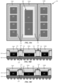
FIG. 2A is a schematic cross-sectional side view illustration of a lid design on an inner and outer support in accordance with an embodiment. -
FIG. 2B is a schematic cross-sectional side view illustration of a lid design on an outer support in accordance with an embodiment. -
FIG. 2C is a schematic top view illustration of the lid design over a module substrate in accordance with an embodiment. -
FIG. 3 is a schematic cross-sectional side view illustration of a trenched design of a lid on an outer support in accordance with an embodiment. -
FIG. 4 is a schematic cross-sectional side view illustration of a partial trenched design of a lid on an inner support in accordance with an embodiment. -
FIG. 5 is a schematic cross-sectional side view illustration of a partial trenched design of a lid on an outer support in accordance with an embodiment. -
FIG. 6 is a schematic cross-sectional side view illustration of a partial trenched design of a lid on both an inner and outer support in accordance with an embodiment. -
FIG. 7 is a schematic cross-sectional side view illustration of a partial trenched design of a lid on an inner or outer support in accordance with an embodiment. -
FIG. 8 is a schematic cross-sectional side view illustration of a stiffener structure formed of adjacent materials with different coefficients of thermal expansion in accordance with an embodiment. -
FIG. 9 is a schematic cross-sectional side view illustration of a stiffener structure formed of stacked materials with different coefficients of thermal expansion in accordance with an embodiment. -
FIG. 10A is a schematic top view illustration of a multiple chip module with multiple piece lid in accordance with an embodiment. -
FIG. 10B is a schematic cross-sectional side view illustration of a multiple piece lid with trench design roof components in accordance with an embodiment. -
FIG. 10C is a schematic cross-sectional side view illustration of a multiple piece lid with a component cavity in accordance with an embodiment. -
FIG. 11A is a schematic top view illustration of a multiple chip module with multiple piece lid in accordance with an embodiment. -
FIG. 11B is a schematic cross-sectional side view illustration of a multiple piece lid with trench design wall components in accordance with an embodiment. -
FIGS. 12A-12B are a schematic cross-sectional side view illustrations of multiple piece lids formed of different materials in accordance with an embodiment. -
FIG. 12C is a schematic top view illustration of a multiple piece lid formed of different materials in accordance with an embodiment. -
FIG. 13A is a schematic cross-sectional side view illustration of a multiple piece lid with sealed gap in accordance with an embodiment. -
FIG. 13B is a schematic top view illustrations of a multiple piece lid with sealed gap in accordance with an embodiment. -
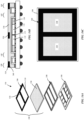
FIG. 14A is an exploded isometric view illustration of a multiple chip module including a hybrid lid design in accordance with an embodiment. -
FIG. 14B is a schematic cross-sectional side view illustration of a multiple chip module including a hybrid lid design in accordance with an embodiment. -
FIG. 14C is schematic top view illustration of a multiple chip module including a hybrid lid design in accordance with an embodiment. -
FIG. 15A is a schematic cross-sectional side view illustration of a lid design on an inner and outer support and including a local opening in accordance with an embodiment. -
FIG. 15B is a schematic cross-sectional side view illustration of a lid design on an outer support and including a local opening in accordance with an embodiment. -
FIG. 15C is a schematic top view illustration of the lid design including a local opening over a module substrate in accordance with an embodiment. -
FIG. 16A is a schematic cross-sectional side view illustration of a lid design on an inner and outer support with the outer connection area overhanging a module substrate in accordance with an embodiment. -
FIG. 16B is a schematic cross-sectional side view illustration of a lid design on an outer support with the outer connection area overhanging a module substrate in accordance with an embodiment. -
FIG. 16C is a schematic top view illustration of the lid design including an outer connection area overhanging a module substrate in one direction in accordance with an embodiment. -
FIG. 16D is a schematic top view illustration of the lid design including an outer connection area overhanging a module substrate in multiple directions in accordance with an embodiment. -
FIG. 16E is a close up schematic cross-sectional side view illustration of a lid and support structure overhanging a module substrate in accordance with an embodiment. -
FIG. 16F is a close up schematic cross-sectional side view illustration of an L-shaped support structure overhanging a module substrate in accordance with an embodiment. -
FIG. 16G is a close up schematic cross-sectional side view illustration of an L-shaped lid overhanging a module substrate in accordance with an embodiment. - While lids can provide mechanical integrity to an MCM, it has been observed that lids can also induce large stress and high warpage in an MCM and induce mechanical failures. For example, lids formed of copper may have a comparatively high coefficient of thermal expansion (CTE) relative to other module features. This can result in thermal expansion and induce stress and warpage in the MCM components (e.g. packages) when the lid is strongly coupled with the rest of the module. In particular, it has been observed that mold cracks can generate between overmolded side-by-side dies, which can be exacerbated by stress induced by a lid. In accordance with embodiments, various combinations of lids and stiffener structures (also referred to as stiffener rings) are provided to balance the ability of the lid to provide mechanical integrity of the module while not inducing mechanical failure.
- In an accordance with embodiments the lid can include a trenched design. The trenched designs may include sufficient lid volume on top of the module components to retain sufficient thermal performance, while volume of the lid is reduced at connection areas to further reduce stress and warpage caused by the lid. In some embodiments a reduction of volume of the lid can correspond to an increase in volume of a stiffener structure, which increases the volume ratio of the stiffener structure to lid. This can further provide feasibility of selecting the stiffener structure material(s) to reduce the stress and warpage in the MCM.
- In accordance with embodiments the stiffener structure (e.g. ring) can be fully or partially formed of a low CTE material. In this aspect an increase of the stiffener structure to lid volume ratio (e.g. due to trenched lid design) facilitates the ability to reduce the effective CTE of the lid-stiffener combination by selecting a stiffener material with a lower CTE than the lid. A reduction of effective CTE of the lid-stiffener structure in turn can reduce stress and warpage issues of the MCM. In an exemplary implementation a low CTE stiffener material can be a nickel-iron alloy (FeNi36), iron-nickel-cobalt alloy (sold under the trademark KOVAR, trademark of CRS Holdings, Inc., Delaware), iron-nickel alloy (Alloy42), stainless steels (SUS410, SUS430), etc. while the lid is formed of a higher CTE material such as copper.
- In accordance with embodiments multiple piece lid designs are described. The multiple piece lid designs may reduce the coupling effect of the lid to the rest of the module, and further reduce stress caused by the lid. This may include a reduction of die-to-die molding compound stress, and module warpage. In some embodiments, the multiple piece lid design incorporates different lid materials to meet different mechanical and thermal requirements of the MCMs. Hybrid lid designs are also described in which lids of different materials are bonded together or embedded, one within the other. By combining different materials, the effective CTE and stiffness of the lid can be tuned to match the target mechanical and thermal performance.
- In various embodiments, description is made with reference to figures. However, certain embodiments may be practiced without one or more of these specific details, or in combination with other known methods and configurations. In the following description, numerous specific details are set forth, such as specific configurations, dimensions and processes, etc., in order to provide a thorough understanding of the embodiments. In other instances, well-known semiconductor processes and manufacturing techniques have not been described in particular detail in order to not unnecessarily obscure the embodiments. Reference throughout this specification to "one embodiment" means that a particular feature, structure, configuration, or characteristic described in connection with the embodiment is included in at least one embodiment. Thus, the appearances of the phrase "in one embodiment" in various places throughout this specification are not necessarily referring to the same embodiment. Furthermore, the particular features, structures, configurations, or characteristics may be combined in any suitable manner in one or more embodiments.
- The terms "above", "over", "to", "between", "spanning" and "on" as used herein may refer to a relative position of one layer with respect to other layers. One layer "above", "over", "spanning" or "on" another layer or bonded "to" or in "contact" with another layer may be directly in contact with the other layer or may have one or more intervening layers. One layer "between" layers may be directly in contact with the layers or may have one or more intervening layers.
- Referring now to
FIG. 1 a cross-sectional side view illustration is provided of anMCM 150 including alid 300 andstiffener structure 200 with inner andouter supports MCM 150 includes amodule substate 100 including atop side 102 andbottom side 104. A plurality offirst components 120 can be mounted on thetop side 102 of themodule substrate 100.First components 120 may be active or passive devices, and may be chips or packages. For example,first components 120 may be memory packages, such as dynamic random-access memory (DRAM) including one or more dies, which can be stacked dies, or side-by-side. In an embodiment, first components are chip scale packages.First components 120 can additionally be different types of components, and need not be identical. One orsecond components 130 can also be mounted on thetop side 102 of themodule substrate 100. In an embodiment, asecond component 130 is a package that includes a plurality (e.g. two or more) of side-by-side dies. For example,second component 130 may include a plurality of side-by-side logic, or system on chip dies. - Referring now to
FIGS. 2A-2C schematic cross-sectional side view and top view illustrations are provided of lid and stiffener structure arrangements in accordance with embodiments. In an exemplary implementation,first components 120 andsecond component 130 are surface mounted onto themodule substate 100 using any suitable technique such as solder bumps 160, with optional underfill 162 (e.g. epoxy). In the illustrated embodiment, thesecond component 130 is a package that includes a plurality of side-by-side dies 132 incapsulated in amolding compound 134. As shown, thespace 133 laterally between the dies 132 may be filled withmolding compound 134. It has been observed this can be a high stress location within the MCM due to close proximity of a variety of materials and MCM structures. - A thermal interface material (TIM) 170 can be located on top sides of the
first components 120 andsecond component 130 in order to secure to thelid 300.TIM 170 may be applied using any suitable technique such as dispensing or tape.Exemplary TIM 170 materials include, but are not limited to, thermal grease, solder, metal filled polymer matrix, etc. - In accordance with embodiments the
lid 300 can be bonded to an intermediate stiffener structure 200 (also referred to as a stiffener ring), which in turn is bonded to themodule substrate 100. Thestiffener structure 200 andlid 300 can be bonded using an adhesive material. For example, and adhesive can be dispensed onto themodule substrate 100 at the connection areas (e.g.outer connection area 180 and inner connection area 182), followed by mounting thestiffener structure 200. Exemplary adhesive materials include glass paste, epoxies, urethane, polyurethane, silicone elastomers, etc. Thelid 300 can similarly be bonded to thestiffener structure 200 after mounting the stiffener structure on themodule substrate 100, or before. - As illustrated the
lid 300 may include aroof 330, outer (periphery)walls 310 and optionallyinner walls 320. Thebottom surface 302 of the roof may be bonded to theTIM 170 on top of thesecond component 130 andfirst components 120. Contour of the bottom surface 302 (thickness of the roof 330) can be adjusted to evenly mate with theTIM 170 for the variousfirst components 120 andsecond component 130. Theouter walls 310 andinner walls 320 can extend from the roof 330 (e.g. protrude from the bottom surface) to form one ormore cavities 305 which accommodate thesecond component 130 andfirst components 120. In accordance with embodiments, thestiffener structure 200 is shaped to mate with theouter walls 310 andinner walls 320 of thelid 300. Specifically, thestiffener structure 200 can include outer support (walls) 210 and inner support 220 (walls).Outer support 210 andinner support 220 may be integrally formed of the same material. Alternatively,outer support 210 andinner support 220 can be formed of different materials with different CTE. A variety of additional configurations, with different materials are possible. The mating surfaces between thestiffener structure 200 andlid 300 may have a same surface area. A plurality of module solder bumps 190 may optionally be applied to thebottom side 104 of themodule substrate 100 for further integration. - In accordance with embodiments, various combinations of lids and stiffener structures are provided to balance the ability of the lid to provide mechanical integrity to the module while not inducing mechanical failure. In particular, various combinations of trenched lid designs, ratios of stiffener structure to lid volume, multiple piece lid designs, and combinations of materials with different CTE are described.
- Referring now to
FIGS. 3-9 various trenched lid designs and stiffener structures are illustrated in accordance with embodiments. As shown, theMCM 150 may include amodule substrate 100, afirst component 120 on thetop side 102 of the module substrate and asecond component 130 on thetop side 102 of the module substrate. Astiffener structure 200 is mounted on thetop side 102 of the module substrate and alid 300 is mounted on thestiffener structure 200 and covering both thefirst component 120 and thesecond component 130. In accordance with various embodiments, thestiffener structure 200 may be joined to thelid 300 within atrench 315 formed in aroof 330 of the lid. Thestiffener structure 200 can include either or both of anouter support 210 and aninner support 220. -
FIG. 3 is a schematic cross-sectional side view illustration of a trenched design of a lid on anouter support 210 in accordance with an embodiment. As shown, atrench 315 is formed in thebottom surface 302 of theroof 330 of thelid 300. Eachtrench 315 may include one or more trench edges (sidewalls) 331 in theroof 330. In this manner, a thickness of theroof 330 in thetrench 315 area is less than a thickness of theroof 330 where thelid 300 is connected to thesecond component 130 withTIM 170, and where thelid 300 is connected to thefirst components 120 with TIM. Thus, thetrench 315 reduces the volume of thelid 300 at the connection area. Specifically, thetrench 315 is formed at the outer (periphery)connection area 180 where the trench is joined with the outer support (walls) 210 of thestiffener structure 200. In this illustration the trench does not include outer sidewalls (trench edge). In the illustrated embodiment theouter support 210 is joined to thelid 300 within thetrench 315. While not illustrated, thelid 300 may additionally include aninner wall 320 joined to aninner support 220 of thestiffener structure 200. -
FIG. 4 is a schematic cross-sectional side view illustration of a partial trenched design of a lid on an inner support in accordance with an embodiment. As shown, theinner support 220 is joined to thelid 300 within thetrench 315. Additionally, thelid 300 includes anouter wall 310 joined to theouter support 210. In the illustrated embodiment theinner support 220 is taller than theouter support 210. -
FIG. 5 is a schematic cross-sectional side view illustration of a partial trenched design of a lid on an outer support in accordance with an embodiment. As shown, theouter support 210 is joined to thelid 300 within the trench. Thelid 300 additionally includes aninner wall 320 joined to theinner support 220. In the illustrated embodiment theouter support 210 is taller than theinner support 220. Also shown inFIG. 5 , theinner wall 320 extends from thetrench 315. In an embodiment, thelid 300 can include bothouter walls 310 andinner walls 320 extending from atrench 315. -
FIG. 6 is a schematic cross-sectional side view illustration of a partial trenched design of a lid on both an inner and outer support in accordance with an embodiment.FIG. 6 is similar to the embodiment illustrated inFIG. 3 with the addition of theinner support 220 also j oined to the lid within atrench 315, which may be the same trench or a separate trench than thetrench 315 where theouter support 210 is joined to the lid. -
FIG. 7 is a schematic cross-sectional side view illustration of a partial trenched design of a lid on an inner or outer support in accordance with an embodiment. As shown,FIG. 7 combines features ofFIGS. 4-6 to show a variety of configurations are possible, where portions of theinner support 220 andouter support 210 can have different heights, andouter wall 310 andinner wall 320 can be discontinuous. - The trenched lid designs in accordance with embodiments can reduce the volume of lid at the connection areas to reduce stress and warpage caused by the lid. Furthermore, the reduction of volume of the lid can correspond to an increase in volume (height) of a stiffener structure, which increases the volume ratio of the stiffener structure to lid. In the illustrated embodiments, the ratio of stiffener structure to lid is greater than 1, meaning the stiffener structure can be taller than a thickness of the trenched roof of the lid.
- In accordance with embodiments the stiffener structure can be fully or partially formed of a low CTE material. In an exemplary implementation a low CTE stiffener material can be a nickel-iron alloy (FeNi36), iron-nickel-cobalt alloy (sold under the trademark KOVAR, trademark of CRS Holdings, Inc., Delaware), iron-nickel alloy (Alloy42), stainless steels (SUS410, SUS430), etc. while the lid is formed of a higher CTE material such as copper. The stiffener structure can also be formed of different materials (different chemical composition, or alloy ratios) to tune stress and warpage.
-
FIG. 8 is a schematic cross-sectional side view illustration of a stiffener structure formed of adjacent materials with different coefficients of thermal expansion in accordance with an embodiment. For example, theouter support 210 and theinner support 220 can be formed ofdifferent materials outer support 210 andinner support 220 can be formed ofdifferent materials -
FIG. 9 is a schematic cross-sectional side view illustration of a stiffener structure formed ofstacked materials materials outer support 210 andinner support 220. - The lids in accordance with embodiments may also have a plurality of physically separate pieces. Such multiple piece lid designs may reduce the coupling effect of the lid to the rest of the module, and further reduce stress caused by the lid. This may include a reduction of die-to-die molding compound stress, and module warpage.
- Referring now to
FIGS. 10A-10C schematic top view and cross-sectional side view illustrations are provided of a multiple piece lid in accordance with embodiments. In the illustrated embodiment thelid 300 may include a plurality of physicallyseparate roofs stiffener structure 200. Theroofs design including trenches 315. In the illustrated embodiments,trenches 315 may be formed along the sides of theroofs inner support 220, and a single roof is bonded to eachouter support 210. Each lid may be anchored to its surroundinginner support 220, and/orouter support 210. In the particular embodiment illustrated inFIG. 10C , the lid may further include acomponent recess 335 which mates with a component (e.g. second component 130) edges. Thecomponent recess 335 may promote coverage of theTIM 170 with the component edges and reduce TIM peeling stress. - Referring now to
FIGS. 11A-11B schematic top view and cross-sectional side view illustrations are provided of a multiple piece lid in accordance with embodiments.FIGS. 11A-11B differ from the embodiment ofFIGS. 10A-10B in that thetrenches 225 are formed within theinner support 220 and/orouter support 210 as opposed to the roofs of the lid. Similarly,trenches 225 may include trench edges 227. In the particular embodiment illustrated, theinner supports 220 includetrenches 225 to accommodate aroof 330A oflid 300. The physicallyseparate roofs FIG. 11A-11B may have different thicknesses to manage stress and warpage. - The multiple piece lid designs in accordance with embodiments may also include inner and/or outer walls. Referring now to
FIGS. 12A-12C schematic cross-sectional side view and top view illustrations are provided of multiple piece lids in accordance with an embodiment. It is to be appreciated that while illustrated and described separately, that the multiple piece lid embodiments ofFIGS. 12A-12C are combinable with the multiple piece lid embodiments ofFIGS. 10A-11B , as well as other embodiments described herein. - As shown the
multiple piece lid 300 may include afirst lid piece 300A spanning over afirst die 132 in thesecond component 130 and asecond lid piece 300B spanning over asecond die 132 in thesecond component 130. Multiple lid pieces may be included 300A, 300B, 300C, 300D, etc. As shown, themolding compound 134 may fill aspace 133 laterally between thefirst die 132 and thesecond die 132, which can correspond to a high stress region. Agap 325 may be located between thefirst lid piece 300A and thesecond lid piece 300B. In the illustrated embodiment thegap 325 is directly above thespace 133 that is laterally between thefirst die 132 and thesecond die 132 of thecomponent 130, which may be filled with themolding compound 134. Thegap 325 may further reduce the coupling effect of the lid to the rest of the module, and further reduce stress caused by the lid. In accordance with embodiments, theseparate lid pieces different materials gap 325 may optionally be filled as shown inFIGS. 13A-13B with afill material 400. For example, the fill material may be a solder, adhesive, etc. - Referring now to
FIGS. 14A-14C exploded isometric, schematic cross-sectional side view, and top view illustrations are provided of a multiple chip module including a hybrid lid design in accordance with embodiments. In addition, or alternative to, the aforementioned structures ahybrid lid 300 design can include different materials bonded together or embedded, one within the other. By combining different materials, the effective CTE and stiffness of the lid can be tuned to match the target mechanical and thermal performance. In an embodiment, alid 300 may include afirst lid pattern 500 bonded to aroof 330 of a main lid structure, wherein thefirst lid pattern 500 has a different CTE than the main lid structure. The main lid structure may be similar to the previously describedlids 300 with the addition of afemale pattern 360 into which thefirst lid pattern 500 is secured. Thefirst lid pattern 500 may include a variety of features, which may optionally include aninner rib 520 and outer (peripheral)contour 510. Thefirst lid pattern 500 may be located at high stress regions, such as at connection areas (180, 182) and over the space between side-by-side dies. In an embodiment, theinner rib 520 is directly over thespace 133 between adjacent dies 132. - Up until this point the lid structures have been illustrated and described as being single or multiple piece lid arrangements. In accordance with embodiments, one or more local openings may be formed in any of the lid structures to reduce stress and warpage.
FIGS. 15A-15C illustrate an exemplary implementation of such alocal opening 326. As shown,FIGS. 15A-15C are similar to the lid design previously illustrated and described with regard toFIGS. 2A-2C , though embodiments are not so limited. In an embodiment, the one or morelocal openings 326 may be located directly above (over) thespace 133 laterally between dies 132. The one or morelocal opening 326 may completely or partially overlap thespace 133. One or more local openings can also be located over other regions to mitigate stress. In an embodiment, the one or morelocal openings 326 are formed completely through theroof 330 of the lid from thetop side 304 to thebottom surface 302 of theroof 330. - The stiffener structure(s) 200 and/or lid(s) 300 can also be designed to overhang peripheral edges of
module substrate 100 to reduce stress and warpage.FIG. 16A is a schematic cross-sectional side view illustration of a lid design on an inner and outer support with theouter connection area 180 overhanging themodule substrate 100 in accordance with an embodiment.FIG. 16B is a schematic cross-sectional side view illustration of a lid design on an outer support with theouter connection area 180 overhanging themodule substrate 100 in accordance with an embodiment. The particular embodiments illustrated inFIGS. 16A-16B are similar to those previously illustrated and described with regard toFIGS. 2A-2B , however, this is merely exemplary and the overhanging designs are combinable with any of thestiffener structure 200 inner andouter supports lid 300 combinations with correspondinginner walls 320 andouter walls 310. The overhanging designs are also compatible with the multiple piece lid structures described herein. - The overhanging lid designs in accordance with embodiments may overhang one or more, or all, peripheral (lateral) edges 106 of the
module substrate 100. In particular, one or moreperipheral edges 216 of thestiffener structure 200 and/orperipheral edges 316 of the lid(s) 300 corresponding to theouter connection areas 180 may overhang one or moreperipheral edges 106 of the module substrate. Specifically, theperipheral edges 216 of theouter supports 210 andperipheral edges 316 of theouter walls 310 of thelids 300 may overhang theperipheral edges 106 of themodule substrate 100.FIG. 16C is a schematic top view illustration of thelid 300 design including an outer connection area overhanging a module substrate in one direction in accordance with an embodiment. As shown, theperipheral edges 316 of thelid 300outer walls 310 extend laterally past theperipheral edges 106 on two opposite sides of themodule substrate 100.FIG. 16D is a schematic top view illustration of thelid 300 design including an outer connection area overhanging a module substrate in multiple directions in accordance with an embodiment. As shown, theperipheral edges 316 of thelid 300outer walls 310 extend laterally past theperipheral edges 106 on four sides of themodule substrate 100. While not visible in the top view illustrations ofFIGS. 16C-16D , theperipheral edges 216 of thestiffener structure 200outer supports 210 can be similarly oriented, or alternatively oriented if thelid 300 does not includeouter walls 310. It is to be appreciated the particular orientations ofFIGS. 16B-16C are exemplary and various alternative arrangements are possible with the outer connection areas to overhang one or moreperipheral edges 106 of the module substrate. Additionally, theouter connection areas 180 may partially or fully overhang a length of any of theperipheral edges 106 of themodule substrate 100. - Referring now to
FIG. 16E a close up schematic cross-sectional side view illustration is provided of alid 300 andsupport structure 200 overhanging a module substrate in accordance with an embodiment. In such a configuration, thebottom side 211 of thesupport structure 200 may be level, or planar. As shown, theperipheral edges support structure 200 andlid 300 overlap (or extend past) theperipheral edge 106 of themodule substrate 100 by a width (W). Thesupport structure 200 and/orlid 300 may also have an L-shape configuration where a hanging portion of the support structure and/orlid 300 is laterally adjacent to aperipheral edge 106 of themodule substrate 100. In such configurations thebottom side 211 of thesupport structure 200 or the bottom side 311 of thelid 300 can have an L-shape profile. -
FIG. 16F is a close up schematic cross-sectional side view illustration of an L-shapedsupport structure 200 overhanging amodule substrate 100 in accordance with an embodiment. As shown, thesupport structure 200 may overlap (or extend past) theperipheral edge 106 of themodule substrate 100 by a width (W), and also include a hangingportion 213 that protrudes downward and is laterally adjacent theperipheral edge 106 of themodule substrate 100. The hangingportion 213 may include aninside edge 217 that is separated from theperipheral edge 106 by a gap (G). -
FIG. 16G is a close up schematic cross-sectional side view illustration of an L-shapedlid 300 overhanging amodule substrate 100 in accordance with an embodiment. As shown, thelid 300 may overlap (or extend past) theperipheral edge 106 of themodule substrate 100 by a width (W), and also include a hangingportion 313 that protrudes downward and is laterally adjacent theperipheral edge 106 of themodule substrate 100. The hangingportion 313 may include an inside edge 317 that is separated from theperipheral edge 106 by a gap (G). - In utilizing the various aspects of the embodiments, it would become apparent to one skilled in the art that combinations or variations of the above embodiments are possible for integrating an MCM lid structure while mitigating module warpage. Although the embodiments have been described in language specific to structural features and/or methodological acts, it is to be understood that the appended claims are not necessarily limited to the specific features or acts described. The specific features and acts disclosed are instead to be understood as embodiments of the claims useful for illustration.
-
- 1. A module comprising:
- a module substrate;
- a first component on a top side of the module substrate;
- a second component on the top side of the module substrate;
- a stiffener structure mounted on the top side of the module substrate; and
- a lid mounted on the stiffener structure and covering the first component and the second component;
- wherein the stiffener structure is joined to the lid within a trench formed in a roof of the lid.
- 2. The module of statement 1, wherein the stiffener structure includes an outer support and an inner support.
- 3. The module of
statement 2, wherein the outer support is joined to the lid within the trench. - 4. The module of
statement 3, wherein the lid comprises an inner wall joined to the inner support of the stiffener structure. - 5. The module of
statement 2, wherein the inner support is joined to the lid within the trench. - 6. The module of statement 5, wherein the lid comprises an outer wall joined to the outer support of the stiffener structure.
- 7. The module of
statement 2, wherein the outer support is joined to the lid within the trench, and the inner support is joined to the lid within a second trench formed in the roof of the lid. - 8. The module of
statement 2, wherein the stiffener structure is formed of a material with a lower CTE than the lid. - 9. The module of
statement 2, wherein the outer support and the inner support of the stiffener structure comprise different materials with a different CTE. - 10. The module of
statement 2, wherein the lid comprises physically separate pieces. - 11. The module of statement 10, wherein the second component comprises a first die and a second die encapsulated within a molding compound and the molding compound fills a space laterally between the first die and the second die.
- 12. The module of statement 11, wherein the lid includes a first lid piece spanning over the first die and a second lid piece spanning over the second die.
- 13. The module of statement 12, wherein the first lid piece has a different chemical composition than the second lid piece.
- 14. The module of statement 12, further comprising a gap between the first lid piece and the second lid piece, wherein the gap is directly above the space laterally between the first die and the second die.
- 15. The module of statement 14, wherein the gap is filled.
- 16. The module of statement 1:
- further comprising a local opening in the roof of the lid;
- wherein the second component comprises a first die and a second die encapsulated within a molding compound and the molding compound fills a space laterally between the first die and the second die; and
- wherein the local opening is directly above a space laterally between the first die and the second die.
- 17. The module of statement 1, wherein a peripheral edge of the lid overhangs a peripheral edge of the module substrate.
- 18. A module comprising:
- a module substrate;
- a first component on a top side of the module substrate;
- a second component on the top side of the module substrate;
- a stiffener structure mounted on the top side of the module substrate; and
- a lid mounted on the stiffener structure and covering the first component and the second component;
- wherein the lid includes a first lid piece spanning over the first component and a second lid piece spanning over the second component.
- 19. The module of statement 18, wherein the second component comprises a first die and a second die encapsulated within a molding compound and the molding compound fills a space laterally between the first die and the second die.
- 20. The module of statement 19, wherein the first lid piece spans over the first die and the second lid piece spans over the second die.
- 21. The module of statement 19, wherein the first lid piece has a different chemical composition than the second lid piece.
- 22. The module of statement 19, further comprising a gap between the first lid piece and the second lid piece, wherein the gap is directly above the space laterally between the first die and the second die.
- 23. The module of statement 22, wherein the gap is filled.
- 24. A module comprising:
- a module substrate;
- a first component on a top side of the module substrate;
- a second component on the top side of the module substrate;
- a stiffener structure mounted on the top side of the module substrate; and
- a lid mounted on the stiffener structure and covering the first component and the second component;
- wherein the lid includes a first lid pattern bonded to a roof of a main lid structure, wherein the first lid pattern has a different CTE than the main lid structure.
- 25. The module of statement 24, wherein the main lid structure includes a female pattern into which the first lid pattern is secured.
Claims (11)
- A module comprising:a module substrate;a first component on a top side of the module substrate;a second component on the top side of the module substrate, wherein the second component comprises a first die and a second die encapsulated within a molding compound and the molding compound fills a space laterally between the first die and the second die;a stiffener structure mounted on the top side of the module substrate; anda lid mounted on the stiffener structure and covering the first component and the second component; anda local opening in the roof of the lid, wherein the local opening is directly above a space laterally between the first die and the second die.
- The module of claim 1, wherein the stiffener structure includes an outer support and an inner support.
- The module of claim 2, wherein the outer support is joined to the lid within a trench formed in a roof of the lid.
- The module of claim 3, wherein the lid comprises an inner wall joined to the inner support of the stiffener structure.
- The module of claim 2, wherein the inner support is joined to the lid within the trench.
- The module of claim 5, wherein the lid comprises an outer wall joined to the outer support of the stiffener structure.
- The module of claim 2, wherein the outer support is joined to the lid within a trench formed in the roof of the lid, and the inner support is joined to the lid within a second trench formed in the roof of the lid.
- The module of claim 2, wherein the stiffener structure is formed of a material with a lower CTE than the lid.
- The module of claim 1, wherein a peripheral edge of the lid overhangs a peripheral edge of the module substrate.
- The module of claim 1, wherein a peripheral edge of the stiffener structure overhangs the peripheral edge of the module substrate.
- The module of claim 1, wherein the local opening is one of a plurality of local openings in the roof of the lid directly above a space laterally between the first die and the second die.
Applications Claiming Priority (4)
| Application Number | Priority Date | Filing Date | Title |
|---|---|---|---|
| US202063002888P | 2020-03-31 | 2020-03-31 | |
| US17/013,279 US11646302B2 (en) | 2020-03-31 | 2020-09-04 | Multiple chip module trenched lid and low coefficient of thermal expansion stiffener ring |
| PCT/US2021/017445 WO2021201990A1 (en) | 2020-03-31 | 2021-02-10 | Multiple chip module with lid and stiffener ring |
| EP21711077.4A EP4128332A1 (en) | 2020-03-31 | 2021-02-10 | Multiple chip module with lid and stiffener ring |
Related Parent Applications (1)
| Application Number | Title | Priority Date | Filing Date |
|---|---|---|---|
| EP21711077.4A Division EP4128332A1 (en) | 2020-03-31 | 2021-02-10 | Multiple chip module with lid and stiffener ring |
Publications (3)
| Publication Number | Publication Date |
|---|---|
| EP4235777A2 true EP4235777A2 (en) | 2023-08-30 |
| EP4235777A3 EP4235777A3 (en) | 2024-02-28 |
| EP4235777B1 EP4235777B1 (en) | 2025-11-26 |
Family
ID=77857563
Family Applications (2)
| Application Number | Title | Priority Date | Filing Date |
|---|---|---|---|
| EP23177407.6A Active EP4235777B1 (en) | 2020-03-31 | 2021-02-10 | Multiple chip module with lid and stiffener ring |
| EP21711077.4A Pending EP4128332A1 (en) | 2020-03-31 | 2021-02-10 | Multiple chip module with lid and stiffener ring |
Family Applications After (1)
| Application Number | Title | Priority Date | Filing Date |
|---|---|---|---|
| EP21711077.4A Pending EP4128332A1 (en) | 2020-03-31 | 2021-02-10 | Multiple chip module with lid and stiffener ring |
Country Status (6)
| Country | Link |
|---|---|
| US (2) | US11646302B2 (en) |
| EP (2) | EP4235777B1 (en) |
| KR (2) | KR102794272B1 (en) |
| CN (2) | CN120957426A (en) |
| TW (2) | TWI773130B (en) |
| WO (1) | WO2021201990A1 (en) |
Families Citing this family (18)
| Publication number | Priority date | Publication date | Assignee | Title |
|---|---|---|---|---|
| JP7235752B2 (en) * | 2018-08-03 | 2023-03-08 | ソニーセミコンダクタソリューションズ株式会社 | semiconductor equipment |
| KR102713128B1 (en) * | 2019-11-15 | 2024-10-07 | 삼성전자주식회사 | Semiconductor Package Having a Stiffener Structure |
| US11646302B2 (en) | 2020-03-31 | 2023-05-09 | Apple Inc. | Multiple chip module trenched lid and low coefficient of thermal expansion stiffener ring |
| US11587887B2 (en) * | 2021-01-14 | 2023-02-21 | Taiwan Semiconductor Manufacturing Company, Ltd. | Semiconductor device and manufacturing method thereof |
| DE102021119360A1 (en) * | 2021-05-05 | 2022-11-10 | Taiwan Semiconductor Manufacturing Co., Ltd. | MULTI-TIM PACKAGES AND THEIR MANUFACTURING PROCESSES |
| US12672541B2 (en) * | 2021-07-23 | 2026-06-30 | Absolics Inc. | Substrate comprising a lid structure, package substrate comprising the same and semiconductor device |
| US12119275B2 (en) | 2021-08-30 | 2024-10-15 | Apple Inc. | Recessed lid and ring designs and lid local peripheral reinforcement designs |
| US12593688B2 (en) * | 2022-08-08 | 2026-03-31 | nD-HI Technologies Lab, Inc. | Manufacturing method of diamond composite wafer |
| US12550737B2 (en) * | 2022-08-30 | 2026-02-10 | Taiwan Semiconductor Manufacturing Co., Ltd. | Semiconductor package and method |
| US12532741B2 (en) * | 2022-11-11 | 2026-01-20 | Amkor Technology Singapore Holding Pte. Ltd. | Semiconductor devices and methods of manufacturing semiconductor devices |
| US20240234304A1 (en) * | 2023-01-06 | 2024-07-11 | Advanced Micro Devices, Inc. | Chip package with core embedded chiplet |
| CN120457542A (en) * | 2023-01-06 | 2025-08-08 | 超威半导体公司 | Chip package with core-embedded chiplet |
| US12557653B2 (en) * | 2023-01-22 | 2026-02-17 | Advanced Micro Devices, Inc. | Package assembly with thermal interface material gutter |
| US12484197B2 (en) * | 2023-03-13 | 2025-11-25 | BorgWarner US Technologies LLC | Systems and methods for a top side cooled power semiconductor thermal interface spacer |
| US20250006572A1 (en) * | 2023-06-29 | 2025-01-02 | Taiwan Semiconductor Manufacturing Company Limited | Package structure including ring structure and methods of forming the same |
| US20250079246A1 (en) * | 2023-09-05 | 2025-03-06 | Taiwan Semiconductor Manufacturing Company, Ltd. | Semiconductor package with stiffener structure |
| US20250105086A1 (en) * | 2023-09-21 | 2025-03-27 | Taiwan Semiconductor Manufacturing Co., Ltd. | Integrated Circuit Packages and Methods of Forming the Same |
| CN119852253A (en) * | 2023-10-09 | 2025-04-18 | 沐曦集成电路(上海)股份有限公司 | Substrate warpage inhibition structure and chip packaging structure |
Citations (1)
| Publication number | Priority date | Publication date | Assignee | Title |
|---|---|---|---|---|
| US20150001701A1 (en) * | 2013-06-27 | 2015-01-01 | International Business Machines Corporation | Multichip module with stiffing frame and associated covers |
Family Cites Families (57)
| Publication number | Priority date | Publication date | Assignee | Title |
|---|---|---|---|---|
| US5900312A (en) | 1996-11-08 | 1999-05-04 | W. L. Gore & Associates, Inc. | Integrated circuit chip package assembly |
| US5881945A (en) * | 1997-04-30 | 1999-03-16 | International Business Machines Corporation | Multi-layer solder seal band for semiconductor substrates and process |
| JP3277996B2 (en) | 1999-06-07 | 2002-04-22 | 日本電気株式会社 | Circuit device and method of manufacturing the same |
| US6437436B2 (en) | 2000-01-20 | 2002-08-20 | Ang Technologies Inc. | Integrated circuit chip package with test points |
| KR100446290B1 (en) * | 2001-11-03 | 2004-09-01 | 삼성전자주식회사 | Semiconductor package having dam and fabricating method the same |
| JP3813540B2 (en) | 2002-05-28 | 2006-08-23 | 富士通株式会社 | Semiconductor device manufacturing method, semiconductor device, and semiconductor device unit |
| JP4390541B2 (en) | 2003-02-03 | 2009-12-24 | Necエレクトロニクス株式会社 | Semiconductor device and manufacturing method thereof |
| JP4526771B2 (en) | 2003-03-14 | 2010-08-18 | 株式会社半導体エネルギー研究所 | Method for manufacturing semiconductor device |
| US7168484B2 (en) | 2003-06-30 | 2007-01-30 | Intel Corporation | Thermal interface apparatus, systems, and methods |
| JP2005116762A (en) | 2003-10-07 | 2005-04-28 | Fujitsu Ltd | Semiconductor device protection method, semiconductor device cover, semiconductor device unit, and semiconductor device packaging structure |
| US7026711B2 (en) | 2003-12-16 | 2006-04-11 | Taiwan Semiconductor Manufacturing Company, Ltd. | Thermal dispensing enhancement for high performance flip chip BGA (HPFCBGA) |
| JP4885425B2 (en) * | 2004-01-28 | 2012-02-29 | 京セラ株式会社 | Semiconductor element storage package |
| TWI239655B (en) | 2004-02-23 | 2005-09-11 | Siliconware Precision Industries Co Ltd | Photosensitive semiconductor package with support member and method for fabricating the same |
| US7038316B2 (en) * | 2004-03-25 | 2006-05-02 | Intel Corporation | Bumpless die and heat spreader lid module bonded to bumped die carrier |
| US7405924B2 (en) | 2004-09-27 | 2008-07-29 | Idc, Llc | System and method for protecting microelectromechanical systems array using structurally reinforced back-plate |
| TWI307942B (en) | 2005-02-18 | 2009-03-21 | Advanced Semiconductor Eng | Tape carrier package and manufacturing method thereof |
| US7585702B1 (en) | 2005-11-08 | 2009-09-08 | Altera Corporation | Structure and assembly procedure for low stress thin die flip chip packages designed for low-K Si and thin core substrate |
| US7440281B2 (en) | 2006-02-01 | 2008-10-21 | Apple Inc. | Thermal interface apparatus |
| US8063482B2 (en) | 2006-06-30 | 2011-11-22 | Intel Corporation | Heat spreader as mechanical reinforcement for ultra-thin die |
| US7489033B2 (en) | 2006-11-10 | 2009-02-10 | Intel Corporation | Electronic assembly with hot spot cooling |
| JP2010103244A (en) | 2008-10-22 | 2010-05-06 | Sony Corp | Semiconductor device, and method of manufacturing the same |
| JP2010103338A (en) | 2008-10-24 | 2010-05-06 | Nec Electronics Corp | Semiconductor device and method of manufacturing same |
| US9202769B2 (en) | 2009-11-25 | 2015-12-01 | Stats Chippac, Ltd. | Semiconductor device and method of forming thermal lid for balancing warpage and thermal management |
| US8299633B2 (en) | 2009-12-21 | 2012-10-30 | Advanced Micro Devices, Inc. | Semiconductor chip device with solder diffusion protection |
| JP5733893B2 (en) * | 2009-12-22 | 2015-06-10 | 新光電気工業株式会社 | Electronic component equipment |
| US8299608B2 (en) | 2010-07-08 | 2012-10-30 | International Business Machines Corporation | Enhanced thermal management of 3-D stacked die packaging |
| US8900927B2 (en) * | 2010-08-16 | 2014-12-02 | International Business Machines Corporation | Multichip electronic packages and methods of manufacture |
| US8976529B2 (en) * | 2011-01-14 | 2015-03-10 | Taiwan Semiconductor Manufacturing Company, Ltd. | Lid design for reliability enhancement in flip chip package |
| US20130001740A1 (en) | 2011-06-30 | 2013-01-03 | Stmicroelectronics Pte Ltd. | Heat spreader for thermally enhanced flip-chip ball grid array package |
| JP5758539B2 (en) | 2012-02-27 | 2015-08-05 | 株式会社フジクラ | Pressure sensor module and lid |
| US9204548B2 (en) | 2012-03-14 | 2015-12-01 | Cisco Technology, Inc | Electronic devices mounted on multiple substrates |
| US9041192B2 (en) | 2012-08-29 | 2015-05-26 | Broadcom Corporation | Hybrid thermal interface material for IC packages with integrated heat spreader |
| US20140091461A1 (en) * | 2012-09-30 | 2014-04-03 | Yuci Shen | Die cap for use with flip chip package |
| US9287233B2 (en) | 2013-12-02 | 2016-03-15 | Taiwan Semiconductor Manufacturing Co., Ltd. | Adhesive pattern for advance package reliability improvement |
| US9269694B2 (en) | 2013-12-11 | 2016-02-23 | Taiwan Semiconductor Manufacturing Company, Ltd. | Packages with thermal management features for reduced thermal crosstalk and methods of forming same |
| US9735043B2 (en) | 2013-12-20 | 2017-08-15 | Taiwan Semiconductor Manufacturing Company, Ltd. | Semiconductor packaging structure and process |
| US10163754B2 (en) * | 2013-12-26 | 2018-12-25 | Taiwan Semiconductor Manufacturing Company, Ltd. | Lid design for heat dissipation enhancement of die package |
| US9831190B2 (en) | 2014-01-09 | 2017-11-28 | Taiwan Semiconductor Manufacturing Co., Ltd. | Semiconductor device package with warpage control structure |
| US9252121B2 (en) | 2014-01-23 | 2016-02-02 | International Business Machines Corporation | Thermal interface material on package |
| US9330999B2 (en) * | 2014-06-05 | 2016-05-03 | Intel Corporation | Multi-component integrated heat spreader for multi-chip packages |
| JP6314731B2 (en) * | 2014-08-01 | 2018-04-25 | 株式会社ソシオネクスト | Semiconductor device and manufacturing method of semiconductor device |
| US10043730B2 (en) * | 2015-09-28 | 2018-08-07 | Xilinx, Inc. | Stacked silicon package assembly having an enhanced lid |
| US9947603B2 (en) | 2015-12-09 | 2018-04-17 | International Business Machines Corporation | Lid attach optimization to limit electronic package warpage |
| US10236229B2 (en) | 2016-06-24 | 2019-03-19 | Xilinx, Inc. | Stacked silicon package assembly having conformal lid |
| KR102588807B1 (en) | 2016-12-15 | 2023-10-13 | 쑤저우 레킨 세미컨덕터 컴퍼니 리미티드 | Semiconductor device package, method for manufacturing semiconductor device package, and auto focusing apparatus |
| US10643938B2 (en) * | 2017-05-31 | 2020-05-05 | Intel Corporation | Standoff spacers for managing bondline thickness in microelectronic packages |
| US11676873B2 (en) | 2017-06-30 | 2023-06-13 | Intel Corporation | Semiconductor package having sealant bridge |
| WO2019066993A1 (en) | 2017-09-30 | 2019-04-04 | Intel Corporation | Warpage mitigation structures created on substrate using high throughput additive manufacturing |
| US11328979B2 (en) | 2017-09-30 | 2022-05-10 | Intel Corporation | Substrate integrated posts and heat spreader customization for enhanced package thermomechanics |
| US10681846B2 (en) | 2018-04-19 | 2020-06-09 | Google Llc | Cooling electronic devices in a data center |
| JP7235752B2 (en) | 2018-08-03 | 2023-03-08 | ソニーセミコンダクタソリューションズ株式会社 | semiconductor equipment |
| US10643924B1 (en) | 2019-05-01 | 2020-05-05 | Yuci Shen | Heat-dissipating lid with reservoir structure and associated lidded flip chip package allowing for liquid thermal interfacing materials |
| KR20200145267A (en) | 2019-06-21 | 2020-12-30 | 삼성전자주식회사 | Semiconductor package |
| US12191220B2 (en) | 2019-10-21 | 2025-01-07 | Intel Corporation | Hybrid interposer of glass and silicon to reduce thermal crosstalk |
| US11646302B2 (en) | 2020-03-31 | 2023-05-09 | Apple Inc. | Multiple chip module trenched lid and low coefficient of thermal expansion stiffener ring |
| US11749631B2 (en) | 2020-05-20 | 2023-09-05 | Apple Inc. | Electronic package including a hybrid thermal interface material and low temperature solder patterns to improve package warpage and reliability |
| US12119275B2 (en) | 2021-08-30 | 2024-10-15 | Apple Inc. | Recessed lid and ring designs and lid local peripheral reinforcement designs |
-
2020
- 2020-09-04 US US17/013,279 patent/US11646302B2/en active Active
-
2021
- 2021-02-08 TW TW110104737A patent/TWI773130B/en active
- 2021-02-08 TW TW111125267A patent/TWI906526B/en active
- 2021-02-10 EP EP23177407.6A patent/EP4235777B1/en active Active
- 2021-02-10 CN CN202511103202.3A patent/CN120957426A/en active Pending
- 2021-02-10 WO PCT/US2021/017445 patent/WO2021201990A1/en not_active Ceased
- 2021-02-10 KR KR1020227027054A patent/KR102794272B1/en active Active
- 2021-02-10 EP EP21711077.4A patent/EP4128332A1/en active Pending
- 2021-02-10 KR KR1020257011105A patent/KR102964478B1/en active Active
- 2021-02-10 CN CN202180015001.1A patent/CN115136298B/en active Active
-
2023
- 2023-03-31 US US18/194,236 patent/US12249599B2/en active Active
Patent Citations (1)
| Publication number | Priority date | Publication date | Assignee | Title |
|---|---|---|---|---|
| US20150001701A1 (en) * | 2013-06-27 | 2015-01-01 | International Business Machines Corporation | Multichip module with stiffing frame and associated covers |
Also Published As
| Publication number | Publication date |
|---|---|
| KR20220124759A (en) | 2022-09-14 |
| US20210305227A1 (en) | 2021-09-30 |
| TWI773130B (en) | 2022-08-01 |
| KR20250054118A (en) | 2025-04-22 |
| TWI906526B (en) | 2025-12-01 |
| US11646302B2 (en) | 2023-05-09 |
| EP4235777A3 (en) | 2024-02-28 |
| WO2021201990A1 (en) | 2021-10-07 |
| US20230317708A1 (en) | 2023-10-05 |
| KR102794272B1 (en) | 2025-04-11 |
| KR102964478B1 (en) | 2026-05-14 |
| CN120957426A (en) | 2025-11-14 |
| TW202147528A (en) | 2021-12-16 |
| EP4235777B1 (en) | 2025-11-26 |
| EP4128332A1 (en) | 2023-02-08 |
| CN115136298A (en) | 2022-09-30 |
| TW202240798A (en) | 2022-10-16 |
| CN115136298B (en) | 2025-09-05 |
| US12249599B2 (en) | 2025-03-11 |
Similar Documents
| Publication | Publication Date | Title |
|---|---|---|
| EP4235777B1 (en) | Multiple chip module with lid and stiffener ring | |
| US11552007B2 (en) | Modified leadframe design with adhesive overflow recesses | |
| KR102275890B1 (en) | Integrated circuit assemblies with reinforcement frames, and methods of manufacture | |
| US7575956B2 (en) | Fabrication method for semiconductor package heat spreaders | |
| KR102772186B1 (en) | Recessed cover and ring designs and cover local perimeter reinforcement designs | |
| CN107978570B (en) | Chip packaging structure and manufacturing method thereof | |
| US20060220187A1 (en) | Heatsink moldlocks | |
| US20200185338A1 (en) | Semiconductor package structure for improving die warpage and manufacturing method thereof | |
| KR100485111B1 (en) | chip size package | |
| US8564115B2 (en) | Package structure having micro-electromechanical element | |
| US20230386961A1 (en) | Semiconductor package and manufacturing method thereof | |
| US20250046674A1 (en) | Recess Island Lid Design for TIM Delamination Risk Mitigation | |
| EP4057339A1 (en) | Base plate having sidewall, power semiconductor module comprising the base plate and method for producing the base plate | |
| CN119275184A (en) | A semiconductor packaging structure | |
| WO2017199278A1 (en) | Semiconductor device |
Legal Events
| Date | Code | Title | Description |
|---|---|---|---|
| PUAI | Public reference made under article 153(3) epc to a published international application that has entered the european phase |
Free format text: ORIGINAL CODE: 0009012 |
|
| STAA | Information on the status of an ep patent application or granted ep patent |
Free format text: STATUS: REQUEST FOR EXAMINATION WAS MADE |
|
| 17P | Request for examination filed |
Effective date: 20230605 |
|
| AC | Divisional application: reference to earlier application |
Ref document number: 4128332 Country of ref document: EP Kind code of ref document: P |
|
| AK | Designated contracting states |
Kind code of ref document: A2 Designated state(s): AL AT BE BG CH CY CZ DE DK EE ES FI FR GB GR HR HU IE IS IT LI LT LU LV MC MK MT NL NO PL PT RO RS SE SI SK SM TR |
|
| REG | Reference to a national code |
Ref country code: DE Ref legal event code: R079 Free format text: PREVIOUS MAIN CLASS: H01L0025065000 Ipc: H01L0023040000 Ref document number: 602021043422 Country of ref document: DE |
|
| PUAL | Search report despatched |
Free format text: ORIGINAL CODE: 0009013 |
|
| AK | Designated contracting states |
Kind code of ref document: A3 Designated state(s): AL AT BE BG CH CY CZ DE DK EE ES FI FR GB GR HR HU IE IS IT LI LT LU LV MC MK MT NL NO PL PT RO RS SE SI SK SM TR |
|
| RIC1 | Information provided on ipc code assigned before grant |
Ipc: H01L 25/03 20060101ALI20240124BHEP Ipc: H01L 23/42 20060101ALI20240124BHEP Ipc: H01L 25/065 20230101ALI20240124BHEP Ipc: H01L 23/367 20060101ALI20240124BHEP Ipc: H01L 23/16 20060101ALI20240124BHEP Ipc: H01L 23/04 20060101AFI20240124BHEP |
|
| STAA | Information on the status of an ep patent application or granted ep patent |
Free format text: STATUS: EXAMINATION IS IN PROGRESS |
|
| 17Q | First examination report despatched |
Effective date: 20241111 |
|
| GRAP | Despatch of communication of intention to grant a patent |
Free format text: ORIGINAL CODE: EPIDOSNIGR1 |
|
| STAA | Information on the status of an ep patent application or granted ep patent |
Free format text: STATUS: GRANT OF PATENT IS INTENDED |
|
| INTG | Intention to grant announced |
Effective date: 20250620 |
|
| GRAS | Grant fee paid |
Free format text: ORIGINAL CODE: EPIDOSNIGR3 |
|
| P01 | Opt-out of the competence of the unified patent court (upc) registered |
Free format text: CASE NUMBER: UPC_APP_6634_4235777/2025 Effective date: 20250910 |
|
| GRAA | (expected) grant |
Free format text: ORIGINAL CODE: 0009210 |
|
| STAA | Information on the status of an ep patent application or granted ep patent |
Free format text: STATUS: THE PATENT HAS BEEN GRANTED |
|
| AC | Divisional application: reference to earlier application |
Ref document number: 4128332 Country of ref document: EP Kind code of ref document: P |
|
| AK | Designated contracting states |
Kind code of ref document: B1 Designated state(s): AL AT BE BG CH CY CZ DE DK EE ES FI FR GB GR HR HU IE IS IT LI LT LU LV MC MK MT NL NO PL PT RO RS SE SI SK SM TR |
|
| REG | Reference to a national code |
Ref country code: CH Ref legal event code: F10 Free format text: ST27 STATUS EVENT CODE: U-0-0-F10-F00 (AS PROVIDED BY THE NATIONAL OFFICE) Effective date: 20251126 Ref country code: GB Ref legal event code: FG4D |
|
| REG | Reference to a national code |
Ref country code: DE Ref legal event code: R079 Ref document number: 602021043422 Country of ref document: DE Free format text: PREVIOUS MAIN CLASS: H01L0023040000 Ipc: H10W0076120000 |
|
| REG | Reference to a national code |
Ref country code: IE Ref legal event code: FG4D |
|
| REG | Reference to a national code |
Ref country code: DE Ref legal event code: R096 Ref document number: 602021043422 Country of ref document: DE |
|
| REG | Reference to a national code |
Ref country code: NL Ref legal event code: MP Effective date: 20251126 |
|
| PG25 | Lapsed in a contracting state [announced via postgrant information from national office to epo] |
Ref country code: ES Free format text: LAPSE BECAUSE OF FAILURE TO SUBMIT A TRANSLATION OF THE DESCRIPTION OR TO PAY THE FEE WITHIN THE PRESCRIBED TIME-LIMIT Effective date: 20251126 |
|
| REG | Reference to a national code |
Ref country code: LT Ref legal event code: MG9D |
|
| PG25 | Lapsed in a contracting state [announced via postgrant information from national office to epo] |
Ref country code: NO Free format text: LAPSE BECAUSE OF FAILURE TO SUBMIT A TRANSLATION OF THE DESCRIPTION OR TO PAY THE FEE WITHIN THE PRESCRIBED TIME-LIMIT Effective date: 20260226 |
|
| PGFP | Annual fee paid to national office [announced via postgrant information from national office to epo] |
Ref country code: DE Payment date: 20260218 Year of fee payment: 6 |
|
| PG25 | Lapsed in a contracting state [announced via postgrant information from national office to epo] |
Ref country code: FI Free format text: LAPSE BECAUSE OF FAILURE TO SUBMIT A TRANSLATION OF THE DESCRIPTION OR TO PAY THE FEE WITHIN THE PRESCRIBED TIME-LIMIT Effective date: 20251126 Ref country code: HR Free format text: LAPSE BECAUSE OF FAILURE TO SUBMIT A TRANSLATION OF THE DESCRIPTION OR TO PAY THE FEE WITHIN THE PRESCRIBED TIME-LIMIT Effective date: 20251126 Ref country code: AT Free format text: LAPSE BECAUSE OF FAILURE TO SUBMIT A TRANSLATION OF THE DESCRIPTION OR TO PAY THE FEE WITHIN THE PRESCRIBED TIME-LIMIT Effective date: 20251126 |
|
| REG | Reference to a national code |
Ref country code: AT Ref legal event code: MK05 Ref document number: 1861978 Country of ref document: AT Kind code of ref document: T Effective date: 20251126 |
|
| PG25 | Lapsed in a contracting state [announced via postgrant information from national office to epo] |
Ref country code: NL Free format text: LAPSE BECAUSE OF FAILURE TO SUBMIT A TRANSLATION OF THE DESCRIPTION OR TO PAY THE FEE WITHIN THE PRESCRIBED TIME-LIMIT Effective date: 20251126 |
|
| PG25 | Lapsed in a contracting state [announced via postgrant information from national office to epo] |
Ref country code: RS Free format text: LAPSE BECAUSE OF FAILURE TO SUBMIT A TRANSLATION OF THE DESCRIPTION OR TO PAY THE FEE WITHIN THE PRESCRIBED TIME-LIMIT Effective date: 20260226 |
|
| PG25 | Lapsed in a contracting state [announced via postgrant information from national office to epo] |
Ref country code: IS Free format text: LAPSE BECAUSE OF FAILURE TO SUBMIT A TRANSLATION OF THE DESCRIPTION OR TO PAY THE FEE WITHIN THE PRESCRIBED TIME-LIMIT Effective date: 20260326 |
|
| PG25 | Lapsed in a contracting state [announced via postgrant information from national office to epo] |
Ref country code: PT Free format text: LAPSE BECAUSE OF FAILURE TO SUBMIT A TRANSLATION OF THE DESCRIPTION OR TO PAY THE FEE WITHIN THE PRESCRIBED TIME-LIMIT Effective date: 20260326 |
|
| PG25 | Lapsed in a contracting state [announced via postgrant information from national office to epo] |
Ref country code: PL Free format text: LAPSE BECAUSE OF FAILURE TO SUBMIT A TRANSLATION OF THE DESCRIPTION OR TO PAY THE FEE WITHIN THE PRESCRIBED TIME-LIMIT Effective date: 20251126 |
|
| PG25 | Lapsed in a contracting state [announced via postgrant information from national office to epo] |
Ref country code: LV Free format text: LAPSE BECAUSE OF FAILURE TO SUBMIT A TRANSLATION OF THE DESCRIPTION OR TO PAY THE FEE WITHIN THE PRESCRIBED TIME-LIMIT Effective date: 20251126 |
|
| PG25 | Lapsed in a contracting state [announced via postgrant information from national office to epo] |
Ref country code: BG Free format text: LAPSE BECAUSE OF FAILURE TO SUBMIT A TRANSLATION OF THE DESCRIPTION OR TO PAY THE FEE WITHIN THE PRESCRIBED TIME-LIMIT Effective date: 20251126 |
|
| PG25 | Lapsed in a contracting state [announced via postgrant information from national office to epo] |
Ref country code: LT Free format text: LAPSE BECAUSE OF FAILURE TO SUBMIT A TRANSLATION OF THE DESCRIPTION OR TO PAY THE FEE WITHIN THE PRESCRIBED TIME-LIMIT Effective date: 20251126 |
|
| PG25 | Lapsed in a contracting state [announced via postgrant information from national office to epo] |
Ref country code: SM Free format text: LAPSE BECAUSE OF FAILURE TO SUBMIT A TRANSLATION OF THE DESCRIPTION OR TO PAY THE FEE WITHIN THE PRESCRIBED TIME-LIMIT Effective date: 20251126 |
|
| PG25 | Lapsed in a contracting state [announced via postgrant information from national office to epo] |
Ref country code: DK Free format text: LAPSE BECAUSE OF FAILURE TO SUBMIT A TRANSLATION OF THE DESCRIPTION OR TO PAY THE FEE WITHIN THE PRESCRIBED TIME-LIMIT Effective date: 20251126 |
|
| PG25 | Lapsed in a contracting state [announced via postgrant information from national office to epo] |
Ref country code: IT Free format text: LAPSE BECAUSE OF FAILURE TO SUBMIT A TRANSLATION OF THE DESCRIPTION OR TO PAY THE FEE WITHIN THE PRESCRIBED TIME-LIMIT Effective date: 20251126 |
|
| PG25 | Lapsed in a contracting state [announced via postgrant information from national office to epo] |
Ref country code: EE Free format text: LAPSE BECAUSE OF FAILURE TO SUBMIT A TRANSLATION OF THE DESCRIPTION OR TO PAY THE FEE WITHIN THE PRESCRIBED TIME-LIMIT Effective date: 20251126 |
|
| PG25 | Lapsed in a contracting state [announced via postgrant information from national office to epo] |
Ref country code: CZ Free format text: LAPSE BECAUSE OF FAILURE TO SUBMIT A TRANSLATION OF THE DESCRIPTION OR TO PAY THE FEE WITHIN THE PRESCRIBED TIME-LIMIT Effective date: 20251126 |
|
| PG25 | Lapsed in a contracting state [announced via postgrant information from national office to epo] |
Ref country code: SK Free format text: LAPSE BECAUSE OF FAILURE TO SUBMIT A TRANSLATION OF THE DESCRIPTION OR TO PAY THE FEE WITHIN THE PRESCRIBED TIME-LIMIT Effective date: 20251126 |
|
| PG25 | Lapsed in a contracting state [announced via postgrant information from national office to epo] |
Ref country code: SE Free format text: LAPSE BECAUSE OF FAILURE TO SUBMIT A TRANSLATION OF THE DESCRIPTION OR TO PAY THE FEE WITHIN THE PRESCRIBED TIME-LIMIT Effective date: 20251126 |