EP4235762A2 - Semiconductor package and method for fabricating base for semiconductor package - Google Patents
Semiconductor package and method for fabricating base for semiconductor package Download PDFInfo
- Publication number
- EP4235762A2 EP4235762A2 EP23173505.1A EP23173505A EP4235762A2 EP 4235762 A2 EP4235762 A2 EP 4235762A2 EP 23173505 A EP23173505 A EP 23173505A EP 4235762 A2 EP4235762 A2 EP 4235762A2
- Authority
- EP
- European Patent Office
- Prior art keywords
- conductive
- base
- semiconductor package
- conductive traces
- layer
- Prior art date
- Legal status (The legal status is an assumption and is not a legal conclusion. Google has not performed a legal analysis and makes no representation as to the accuracy of the status listed.)
- Pending
Links
- 239000004065 semiconductor Substances 0.000 title claims abstract description 139
- 238000000034 method Methods 0.000 title abstract description 85
- 239000010410 layer Substances 0.000 claims description 125
- RYGMFSIKBFXOCR-UHFFFAOYSA-N Copper Chemical compound [Cu] RYGMFSIKBFXOCR-UHFFFAOYSA-N 0.000 claims description 29
- 229910052802 copper Inorganic materials 0.000 claims description 29
- 239000010949 copper Substances 0.000 claims description 29
- 229910000679 solder Inorganic materials 0.000 claims description 28
- 229910052751 metal Inorganic materials 0.000 claims description 17
- 239000002184 metal Substances 0.000 claims description 17
- 239000002356 single layer Substances 0.000 claims description 7
- 238000005272 metallurgy Methods 0.000 claims description 4
- 239000000463 material Substances 0.000 description 40
- 238000007747 plating Methods 0.000 description 20
- 238000009413 insulation Methods 0.000 description 19
- 238000005530 etching Methods 0.000 description 17
- 238000005553 drilling Methods 0.000 description 16
- 239000012774 insulation material Substances 0.000 description 11
- 239000000758 substrate Substances 0.000 description 11
- 238000013461 design Methods 0.000 description 5
- 239000004743 Polypropylene Substances 0.000 description 4
- 238000010030 laminating Methods 0.000 description 4
- 229920001155 polypropylene Polymers 0.000 description 4
- 230000015572 biosynthetic process Effects 0.000 description 3
- 238000005516 engineering process Methods 0.000 description 3
- 229920002120 photoresistant polymer Polymers 0.000 description 3
- 239000004020 conductor Substances 0.000 description 2
- 238000009713 electroplating Methods 0.000 description 2
- 238000012986 modification Methods 0.000 description 2
- 230000004048 modification Effects 0.000 description 2
- 238000004806 packaging method and process Methods 0.000 description 2
- -1 polypropylene Polymers 0.000 description 2
- 239000004593 Epoxy Substances 0.000 description 1
- 239000004642 Polyimide Substances 0.000 description 1
- 229910052581 Si3N4 Inorganic materials 0.000 description 1
- VYPSYNLAJGMNEJ-UHFFFAOYSA-N Silicium dioxide Chemical compound O=[Si]=O VYPSYNLAJGMNEJ-UHFFFAOYSA-N 0.000 description 1
- XUIMIQQOPSSXEZ-UHFFFAOYSA-N Silicon Chemical compound [Si] XUIMIQQOPSSXEZ-UHFFFAOYSA-N 0.000 description 1
- RTAQQCXQSZGOHL-UHFFFAOYSA-N Titanium Chemical compound [Ti] RTAQQCXQSZGOHL-UHFFFAOYSA-N 0.000 description 1
- 229910045601 alloy Inorganic materials 0.000 description 1
- 239000000956 alloy Substances 0.000 description 1
- 229910052782 aluminium Inorganic materials 0.000 description 1
- XAGFODPZIPBFFR-UHFFFAOYSA-N aluminium Chemical compound [Al] XAGFODPZIPBFFR-UHFFFAOYSA-N 0.000 description 1
- 230000004888 barrier function Effects 0.000 description 1
- 230000003139 buffering effect Effects 0.000 description 1
- 238000004891 communication Methods 0.000 description 1
- 238000000151 deposition Methods 0.000 description 1
- 238000011161 development Methods 0.000 description 1
- 239000011521 glass Substances 0.000 description 1
- PCHJSUWPFVWCPO-UHFFFAOYSA-N gold Chemical compound [Au] PCHJSUWPFVWCPO-UHFFFAOYSA-N 0.000 description 1
- 239000010931 gold Substances 0.000 description 1
- 229910052737 gold Inorganic materials 0.000 description 1
- 230000017525 heat dissipation Effects 0.000 description 1
- 239000011229 interlayer Substances 0.000 description 1
- 239000007788 liquid Substances 0.000 description 1
- 238000002161 passivation Methods 0.000 description 1
- 229920001721 polyimide Polymers 0.000 description 1
- 238000007650 screen-printing Methods 0.000 description 1
- 238000012216 screening Methods 0.000 description 1
- 238000000926 separation method Methods 0.000 description 1
- 229910052710 silicon Inorganic materials 0.000 description 1
- 239000010703 silicon Substances 0.000 description 1
- HQVNEWCFYHHQES-UHFFFAOYSA-N silicon nitride Chemical compound N12[Si]34N5[Si]62N3[Si]51N64 HQVNEWCFYHHQES-UHFFFAOYSA-N 0.000 description 1
- 229910052814 silicon oxide Inorganic materials 0.000 description 1
- 238000004544 sputter deposition Methods 0.000 description 1
- 239000010935 stainless steel Substances 0.000 description 1
- 229910001220 stainless steel Inorganic materials 0.000 description 1
- 239000010936 titanium Substances 0.000 description 1
- 229910052719 titanium Inorganic materials 0.000 description 1
Images


Classifications
-
- H—ELECTRICITY
- H01—ELECTRIC ELEMENTS
- H01L—SEMICONDUCTOR DEVICES NOT COVERED BY CLASS H10
- H01L24/00—Arrangements for connecting or disconnecting semiconductor or solid-state bodies; Methods or apparatus related thereto
- H01L24/01—Means for bonding being attached to, or being formed on, the surface to be connected, e.g. chip-to-package, die-attach, "first-level" interconnects; Manufacturing methods related thereto
- H01L24/10—Bump connectors ; Manufacturing methods related thereto
- H01L24/15—Structure, shape, material or disposition of the bump connectors after the connecting process
- H01L24/16—Structure, shape, material or disposition of the bump connectors after the connecting process of an individual bump connector
-
- H—ELECTRICITY
- H01—ELECTRIC ELEMENTS
- H01L—SEMICONDUCTOR DEVICES NOT COVERED BY CLASS H10
- H01L23/00—Details of semiconductor or other solid state devices
- H01L23/48—Arrangements for conducting electric current to or from the solid state body in operation, e.g. leads, terminal arrangements ; Selection of materials therefor
- H01L23/488—Arrangements for conducting electric current to or from the solid state body in operation, e.g. leads, terminal arrangements ; Selection of materials therefor consisting of soldered or bonded constructions
- H01L23/495—Lead-frames or other flat leads
- H01L23/49541—Geometry of the lead-frame
-
- H—ELECTRICITY
- H01—ELECTRIC ELEMENTS
- H01L—SEMICONDUCTOR DEVICES NOT COVERED BY CLASS H10
- H01L21/00—Processes or apparatus adapted for the manufacture or treatment of semiconductor or solid state devices or of parts thereof
- H01L21/02—Manufacture or treatment of semiconductor devices or of parts thereof
- H01L21/04—Manufacture or treatment of semiconductor devices or of parts thereof the devices having at least one potential-jump barrier or surface barrier, e.g. PN junction, depletion layer or carrier concentration layer
- H01L21/48—Manufacture or treatment of parts, e.g. containers, prior to assembly of the devices, using processes not provided for in a single one of the subgroups H01L21/06 - H01L21/326
- H01L21/4814—Conductive parts
- H01L21/4846—Leads on or in insulating or insulated substrates, e.g. metallisation
- H01L21/4857—Multilayer substrates
-
- H—ELECTRICITY
- H01—ELECTRIC ELEMENTS
- H01L—SEMICONDUCTOR DEVICES NOT COVERED BY CLASS H10
- H01L21/00—Processes or apparatus adapted for the manufacture or treatment of semiconductor or solid state devices or of parts thereof
- H01L21/67—Apparatus specially adapted for handling semiconductor or electric solid state devices during manufacture or treatment thereof; Apparatus specially adapted for handling wafers during manufacture or treatment of semiconductor or electric solid state devices or components ; Apparatus not specifically provided for elsewhere
- H01L21/683—Apparatus specially adapted for handling semiconductor or electric solid state devices during manufacture or treatment thereof; Apparatus specially adapted for handling wafers during manufacture or treatment of semiconductor or electric solid state devices or components ; Apparatus not specifically provided for elsewhere for supporting or gripping
- H01L21/6835—Apparatus specially adapted for handling semiconductor or electric solid state devices during manufacture or treatment thereof; Apparatus specially adapted for handling wafers during manufacture or treatment of semiconductor or electric solid state devices or components ; Apparatus not specifically provided for elsewhere for supporting or gripping using temporarily an auxiliary support
-
- H—ELECTRICITY
- H01—ELECTRIC ELEMENTS
- H01L—SEMICONDUCTOR DEVICES NOT COVERED BY CLASS H10
- H01L23/00—Details of semiconductor or other solid state devices
- H01L23/48—Arrangements for conducting electric current to or from the solid state body in operation, e.g. leads, terminal arrangements ; Selection of materials therefor
- H01L23/488—Arrangements for conducting electric current to or from the solid state body in operation, e.g. leads, terminal arrangements ; Selection of materials therefor consisting of soldered or bonded constructions
- H01L23/498—Leads, i.e. metallisations or lead-frames on insulating substrates, e.g. chip carriers
- H01L23/49822—Multilayer substrates
-
- H—ELECTRICITY
- H01—ELECTRIC ELEMENTS
- H01L—SEMICONDUCTOR DEVICES NOT COVERED BY CLASS H10
- H01L28/00—Passive two-terminal components without a potential-jump or surface barrier for integrated circuits; Details thereof; Multistep manufacturing processes therefor
-
- H—ELECTRICITY
- H01—ELECTRIC ELEMENTS
- H01L—SEMICONDUCTOR DEVICES NOT COVERED BY CLASS H10
- H01L2221/00—Processes or apparatus adapted for the manufacture or treatment of semiconductor or solid state devices or of parts thereof covered by H01L21/00
- H01L2221/67—Apparatus for handling semiconductor or electric solid state devices during manufacture or treatment thereof; Apparatus for handling wafers during manufacture or treatment of semiconductor or electric solid state devices or components; Apparatus not specifically provided for elsewhere
- H01L2221/683—Apparatus for handling semiconductor or electric solid state devices during manufacture or treatment thereof; Apparatus for handling wafers during manufacture or treatment of semiconductor or electric solid state devices or components; Apparatus not specifically provided for elsewhere for supporting or gripping
- H01L2221/68304—Apparatus for handling semiconductor or electric solid state devices during manufacture or treatment thereof; Apparatus for handling wafers during manufacture or treatment of semiconductor or electric solid state devices or components; Apparatus not specifically provided for elsewhere for supporting or gripping using temporarily an auxiliary support
- H01L2221/68345—Apparatus for handling semiconductor or electric solid state devices during manufacture or treatment thereof; Apparatus for handling wafers during manufacture or treatment of semiconductor or electric solid state devices or components; Apparatus not specifically provided for elsewhere for supporting or gripping using temporarily an auxiliary support used as a support during the manufacture of self supporting substrates
-
- H—ELECTRICITY
- H01—ELECTRIC ELEMENTS
- H01L—SEMICONDUCTOR DEVICES NOT COVERED BY CLASS H10
- H01L2224/00—Indexing scheme for arrangements for connecting or disconnecting semiconductor or solid-state bodies and methods related thereto as covered by H01L24/00
- H01L2224/01—Means for bonding being attached to, or being formed on, the surface to be connected, e.g. chip-to-package, die-attach, "first-level" interconnects; Manufacturing methods related thereto
- H01L2224/02—Bonding areas; Manufacturing methods related thereto
- H01L2224/04—Structure, shape, material or disposition of the bonding areas prior to the connecting process
- H01L2224/0401—Bonding areas specifically adapted for bump connectors, e.g. under bump metallisation [UBM]
-
- H—ELECTRICITY
- H01—ELECTRIC ELEMENTS
- H01L—SEMICONDUCTOR DEVICES NOT COVERED BY CLASS H10
- H01L2224/00—Indexing scheme for arrangements for connecting or disconnecting semiconductor or solid-state bodies and methods related thereto as covered by H01L24/00
- H01L2224/01—Means for bonding being attached to, or being formed on, the surface to be connected, e.g. chip-to-package, die-attach, "first-level" interconnects; Manufacturing methods related thereto
- H01L2224/02—Bonding areas; Manufacturing methods related thereto
- H01L2224/04—Structure, shape, material or disposition of the bonding areas prior to the connecting process
- H01L2224/05—Structure, shape, material or disposition of the bonding areas prior to the connecting process of an individual bonding area
- H01L2224/0554—External layer
- H01L2224/0556—Disposition
- H01L2224/05571—Disposition the external layer being disposed in a recess of the surface
- H01L2224/05572—Disposition the external layer being disposed in a recess of the surface the external layer extending out of an opening
-
- H—ELECTRICITY
- H01—ELECTRIC ELEMENTS
- H01L—SEMICONDUCTOR DEVICES NOT COVERED BY CLASS H10
- H01L2224/00—Indexing scheme for arrangements for connecting or disconnecting semiconductor or solid-state bodies and methods related thereto as covered by H01L24/00
- H01L2224/01—Means for bonding being attached to, or being formed on, the surface to be connected, e.g. chip-to-package, die-attach, "first-level" interconnects; Manufacturing methods related thereto
- H01L2224/10—Bump connectors; Manufacturing methods related thereto
- H01L2224/12—Structure, shape, material or disposition of the bump connectors prior to the connecting process
- H01L2224/13—Structure, shape, material or disposition of the bump connectors prior to the connecting process of an individual bump connector
- H01L2224/13001—Core members of the bump connector
- H01L2224/13075—Plural core members
- H01L2224/1308—Plural core members being stacked
- H01L2224/13083—Three-layer arrangements
-
- H—ELECTRICITY
- H01—ELECTRIC ELEMENTS
- H01L—SEMICONDUCTOR DEVICES NOT COVERED BY CLASS H10
- H01L2224/00—Indexing scheme for arrangements for connecting or disconnecting semiconductor or solid-state bodies and methods related thereto as covered by H01L24/00
- H01L2224/01—Means for bonding being attached to, or being formed on, the surface to be connected, e.g. chip-to-package, die-attach, "first-level" interconnects; Manufacturing methods related thereto
- H01L2224/10—Bump connectors; Manufacturing methods related thereto
- H01L2224/15—Structure, shape, material or disposition of the bump connectors after the connecting process
- H01L2224/16—Structure, shape, material or disposition of the bump connectors after the connecting process of an individual bump connector
- H01L2224/161—Disposition
- H01L2224/16151—Disposition the bump connector connecting between a semiconductor or solid-state body and an item not being a semiconductor or solid-state body, e.g. chip-to-substrate, chip-to-passive
- H01L2224/16221—Disposition the bump connector connecting between a semiconductor or solid-state body and an item not being a semiconductor or solid-state body, e.g. chip-to-substrate, chip-to-passive the body and the item being stacked
- H01L2224/16225—Disposition the bump connector connecting between a semiconductor or solid-state body and an item not being a semiconductor or solid-state body, e.g. chip-to-substrate, chip-to-passive the body and the item being stacked the item being non-metallic, e.g. insulating substrate with or without metallisation
- H01L2224/16237—Disposition the bump connector connecting between a semiconductor or solid-state body and an item not being a semiconductor or solid-state body, e.g. chip-to-substrate, chip-to-passive the body and the item being stacked the item being non-metallic, e.g. insulating substrate with or without metallisation the bump connector connecting to a bonding area disposed in a recess of the surface of the item
-
- H—ELECTRICITY
- H01—ELECTRIC ELEMENTS
- H01L—SEMICONDUCTOR DEVICES NOT COVERED BY CLASS H10
- H01L2224/00—Indexing scheme for arrangements for connecting or disconnecting semiconductor or solid-state bodies and methods related thereto as covered by H01L24/00
- H01L2224/01—Means for bonding being attached to, or being formed on, the surface to be connected, e.g. chip-to-package, die-attach, "first-level" interconnects; Manufacturing methods related thereto
- H01L2224/10—Bump connectors; Manufacturing methods related thereto
- H01L2224/15—Structure, shape, material or disposition of the bump connectors after the connecting process
- H01L2224/16—Structure, shape, material or disposition of the bump connectors after the connecting process of an individual bump connector
- H01L2224/161—Disposition
- H01L2224/16151—Disposition the bump connector connecting between a semiconductor or solid-state body and an item not being a semiconductor or solid-state body, e.g. chip-to-substrate, chip-to-passive
- H01L2224/16221—Disposition the bump connector connecting between a semiconductor or solid-state body and an item not being a semiconductor or solid-state body, e.g. chip-to-substrate, chip-to-passive the body and the item being stacked
- H01L2224/16225—Disposition the bump connector connecting between a semiconductor or solid-state body and an item not being a semiconductor or solid-state body, e.g. chip-to-substrate, chip-to-passive the body and the item being stacked the item being non-metallic, e.g. insulating substrate with or without metallisation
- H01L2224/16238—Disposition the bump connector connecting between a semiconductor or solid-state body and an item not being a semiconductor or solid-state body, e.g. chip-to-substrate, chip-to-passive the body and the item being stacked the item being non-metallic, e.g. insulating substrate with or without metallisation the bump connector connecting to a bonding area protruding from the surface of the item
-
- H—ELECTRICITY
- H01—ELECTRIC ELEMENTS
- H01L—SEMICONDUCTOR DEVICES NOT COVERED BY CLASS H10
- H01L2224/00—Indexing scheme for arrangements for connecting or disconnecting semiconductor or solid-state bodies and methods related thereto as covered by H01L24/00
- H01L2224/73—Means for bonding being of different types provided for in two or more of groups H01L2224/10, H01L2224/18, H01L2224/26, H01L2224/34, H01L2224/42, H01L2224/50, H01L2224/63, H01L2224/71
- H01L2224/732—Location after the connecting process
- H01L2224/73201—Location after the connecting process on the same surface
- H01L2224/73203—Bump and layer connectors
- H01L2224/73204—Bump and layer connectors the bump connector being embedded into the layer connector
-
- H—ELECTRICITY
- H01—ELECTRIC ELEMENTS
- H01L—SEMICONDUCTOR DEVICES NOT COVERED BY CLASS H10
- H01L2224/00—Indexing scheme for arrangements for connecting or disconnecting semiconductor or solid-state bodies and methods related thereto as covered by H01L24/00
- H01L2224/80—Methods for connecting semiconductor or other solid state bodies using means for bonding being attached to, or being formed on, the surface to be connected
- H01L2224/81—Methods for connecting semiconductor or other solid state bodies using means for bonding being attached to, or being formed on, the surface to be connected using a bump connector
- H01L2224/8119—Arrangement of the bump connectors prior to mounting
- H01L2224/81191—Arrangement of the bump connectors prior to mounting wherein the bump connectors are disposed only on the semiconductor or solid-state body
-
- H—ELECTRICITY
- H01—ELECTRIC ELEMENTS
- H01L—SEMICONDUCTOR DEVICES NOT COVERED BY CLASS H10
- H01L2224/00—Indexing scheme for arrangements for connecting or disconnecting semiconductor or solid-state bodies and methods related thereto as covered by H01L24/00
- H01L2224/80—Methods for connecting semiconductor or other solid state bodies using means for bonding being attached to, or being formed on, the surface to be connected
- H01L2224/81—Methods for connecting semiconductor or other solid state bodies using means for bonding being attached to, or being formed on, the surface to be connected using a bump connector
- H01L2224/8138—Bonding interfaces outside the semiconductor or solid-state body
- H01L2224/81385—Shape, e.g. interlocking features
-
- H—ELECTRICITY
- H01—ELECTRIC ELEMENTS
- H01L—SEMICONDUCTOR DEVICES NOT COVERED BY CLASS H10
- H01L23/00—Details of semiconductor or other solid state devices
- H01L23/48—Arrangements for conducting electric current to or from the solid state body in operation, e.g. leads, terminal arrangements ; Selection of materials therefor
- H01L23/488—Arrangements for conducting electric current to or from the solid state body in operation, e.g. leads, terminal arrangements ; Selection of materials therefor consisting of soldered or bonded constructions
- H01L23/498—Leads, i.e. metallisations or lead-frames on insulating substrates, e.g. chip carriers
- H01L23/49811—Additional leads joined to the metallisation on the insulating substrate, e.g. pins, bumps, wires, flat leads
-
- H—ELECTRICITY
- H01—ELECTRIC ELEMENTS
- H01L—SEMICONDUCTOR DEVICES NOT COVERED BY CLASS H10
- H01L23/00—Details of semiconductor or other solid state devices
- H01L23/48—Arrangements for conducting electric current to or from the solid state body in operation, e.g. leads, terminal arrangements ; Selection of materials therefor
- H01L23/488—Arrangements for conducting electric current to or from the solid state body in operation, e.g. leads, terminal arrangements ; Selection of materials therefor consisting of soldered or bonded constructions
- H01L23/498—Leads, i.e. metallisations or lead-frames on insulating substrates, e.g. chip carriers
- H01L23/49827—Via connections through the substrates, e.g. pins going through the substrate, coaxial cables
-
- H—ELECTRICITY
- H01—ELECTRIC ELEMENTS
- H01L—SEMICONDUCTOR DEVICES NOT COVERED BY CLASS H10
- H01L24/00—Arrangements for connecting or disconnecting semiconductor or solid-state bodies; Methods or apparatus related thereto
- H01L24/01—Means for bonding being attached to, or being formed on, the surface to be connected, e.g. chip-to-package, die-attach, "first-level" interconnects; Manufacturing methods related thereto
- H01L24/10—Bump connectors ; Manufacturing methods related thereto
- H01L24/12—Structure, shape, material or disposition of the bump connectors prior to the connecting process
- H01L24/13—Structure, shape, material or disposition of the bump connectors prior to the connecting process of an individual bump connector
-
- H—ELECTRICITY
- H01—ELECTRIC ELEMENTS
- H01L—SEMICONDUCTOR DEVICES NOT COVERED BY CLASS H10
- H01L24/00—Arrangements for connecting or disconnecting semiconductor or solid-state bodies; Methods or apparatus related thereto
- H01L24/80—Methods for connecting semiconductor or other solid state bodies using means for bonding being attached to, or being formed on, the surface to be connected
- H01L24/81—Methods for connecting semiconductor or other solid state bodies using means for bonding being attached to, or being formed on, the surface to be connected using a bump connector
-
- H—ELECTRICITY
- H01—ELECTRIC ELEMENTS
- H01L—SEMICONDUCTOR DEVICES NOT COVERED BY CLASS H10
- H01L2924/00—Indexing scheme for arrangements or methods for connecting or disconnecting semiconductor or solid-state bodies as covered by H01L24/00
- H01L2924/10—Details of semiconductor or other solid state devices to be connected
- H01L2924/11—Device type
- H01L2924/12—Passive devices, e.g. 2 terminal devices
- H01L2924/1204—Optical Diode
- H01L2924/12042—LASER
Definitions
- the present invention relates to a semiconductor package and a method for fabricating a base for a semiconductor package, and in particular, to a base for a high density semiconductor package.
- semiconductor packages are desired to be small in size, to support multi-pin connection, to support high speeds, and to support high functionality.
- I/O Input-Output
- Flip-chip technology uses bumps on a chip to interconnect to a package substrate.
- the flip-chip is bonded face down to the package substrate through the shortest path.
- the technology used can be applied not only to a single-chip package, but also to higher or integrated levels of packaging in which the packages are larger and packaged with more sophisticated substrates that accommodate several chips to form larger functional units.
- the flip-chip technique using an area array, can achieve a high density interconnection with devices and a very low inductance interconnection with packaging.
- PCB printed circuit board
- DCA direct chip attach
- the increased amount of input/output connections of a multifunctional flip-chip package may induce thermal electrical problems, for example, problems with heat dissipation, cross talk, signal propagation delay, electromagnetic interference for RF circuits, etc.
- the thermal electrical problems may affect the reliability and quality of products.
- US 2010/0175917 A1 discloses a semiconductor device in which a chip is mounted on a wiring board.
- the chip is mounted on pads formed in a wiring layer of the wiring board by means of solder bumps.
- US 2008/0246146 A1 describes a semiconductor chip mounted on a support plate through an insulating layer by means of solder bumps made of solder and connected to underlying electrode pads having a layer structure including a gold layer and a layer and via conductive patterns formed in the insulating layer .
- a semiconductor chip mounted on a built-up structure by means of solder bumps and metal bumps is know from US 2011/0097850 A1 .
- electrode pads are used for mounting a semiconductor device on a base.
- contact pads are employed on a carrier substrate for mounting a die on a PCB via solder bumps.
- US 2008/145967 A1 describes a plurality of package traces embedded in an insulating layer.
- This document discloses a trace layer with a bottom surface and sidewalls connected to an insulating layer and with top surface that is aligned with a surface of the insulating layer in which the solder is embedded.
- This same document also discloses a trace embedded in an insulating layer having a top surface below a surface of the insulating layer but without having a bottom surface fully connected to the insulating layer.
- US 2009/0250811 A1 describes a trace line having a top surface aligned with a surface of a surrounding substrate in which the trace line is embedded and trace lines that are not embedded in an underlying substrate.
- US 2011/013334 A1 likewise discloses a trace line having a top surface aligned with a surface of a surrounding substrate in which the trace line is embedded and trace lines that are not embedded in an underlying substrate.
- US 7 589 398 B1 teaches using out-of-plane traces protruding from a base as screening elements for shielding adjacent in-plane traces embedded in the base.
- An exemplary embodiment of a semiconductor package includes a conductive trace embedded in a base.
- a semiconductor device is mounted on the conductive trace via a conductive structure.
- Another exemplary embodiment of a semiconductor package includes a conductive trace, having a bottom surface and at least a portion of a sidewall connected to a base.
- a semiconductor device is mounted on the conductive trace via a conductive structure.
- An exemplary embodiment of a method for fabricating a base for a semiconductor package includes providing a carrier with conductive seed layers on a top surface and a bottom surface of the carrier.
- First conductive traces are respectively formed on the top surface and the bottom surface of the carrier, connecting to the conductive seed layers.
- a first base material layer and a second base material layer are respectively laminated on the top surface and the bottom surface of the carrier, covering the first conductive traces.
- Second conductive traces are respectively formed on first surfaces of the first base material layer and the second base material layer, wherein the first surfaces of the first base material layer and the second base material layer are respectively away from the top surface and the bottom surface of the carrier.
- the first base material layer with the first and second conductive traces thereon and the second base material layer with the first and second conductive traces thereon are separated from the carrier to form a first base and a second base.
- Another exemplary embodiment of a method for fabricating a semiconductor package includes providing a base, forming a conductive trace on the base, further forming an additional insulation material on the base, and further defining patterns upon the additional insulation material, wherein the pattern is formed on at least one conductive trace.
- FIGS. 1 to 4 show cross sections of various exemplary embodiments of a semiconductor package of the invention.
- the semiconductor package can be a flip chip package using conductive structures, for example, copper pillar bumps, connecting a semiconductor device to a base.
- the semiconductor package can be a package using wire bonding technology to connect a semiconductor device to a base.
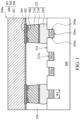
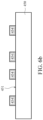
- FIG. 1 shows a partial cross section of one exemplary embodiment of a semiconductor package 500a of the invention. Please refer to FIG. 1 , wherein the semiconductor package 500a comprises a base 200 having a device attach surface 214.
- the base 200 for example, a print circuit board (PCB), may be formed of polypropylene (PP).
- PCB print circuit board
- the base 200 can be a single layer or a multilayer structure.
- a plurality of conductive traces 202a is embedded in the base 200.
- the conductive traces 202a may comprise signal trace segments or ground trace segments, which are used for input/output (I/O) connections of a semiconductor device 300 mounted directly onto the base 200. Therefore, each of the conductive traces 202a has a portion serving as a pad region of the base 200.
- the conductive traces 202a are designed to have a width which is larger than 5 ⁇ m. However, it should be noted that there is no limitation on the width of the conductive traces. For different designs, the width of the conductive traces can be smaller than 5 ⁇ m if required.
- a semiconductor device 300 is mounted on the device attach surface 214 of the base 200 with an active surface of the semiconductor device 300 facing the base 200 by a bonding process.
- the semiconductor device 300 may comprise a die, a passive component, a package or a wafer level package.
- the semiconductor device 300 is a flip chip package.
- a circuitry of the semiconductor device 300 is disposed on the active surface, and metal pads 304 are disposed on a top of the circuitry.
- the circuitry of the semiconductor device 300 is interconnected to the circuitry of the base 200 via a plurality of conductive structures 222 disposed on the active surface of the semiconductor device 300.
- the conductive structures 222 shown in Fig.1 is only an example and is not a limitation to the present invention.
- the semiconductor device 300 may include a body 301, metal pads 304 overlying the semiconductor body 301, and an insulation layer 302 covering the metal pads 304.
- the semiconductor body 301 may include but is not limited to a semiconductor substrate, circuit elements fabricated on the main surface of the semiconductor substrate, inter-layer dielectric (ILD) layers and an interconnection structure.
- the interconnection structure may comprise a plurality of metal layers, a plurality of dielectric layers alternatively laminated with the metal layers and a plurality of vias formed through the dielectric layers on the semiconductor substrate.
- the metal pads 304 comprise the topmost metal layer of the metal layers of the interconnection structure.
- the insulation layer 302 may be a single layer structure or a multilayer structure, and the insulation layer 302 may comprise but is not limited to silicon nitride, silicon oxide, silicon oxynitride, polyimide or any combination thereof. Also, the insulation layer 302 may have functions of stress buffering and insulation.
- the metal pad 304 may comprise but is not limited to aluminum, copper or alloys thereof. A plurality of openings can be formed in the insulation layer 302. Each of the openings exposes at least a portion of one of the metal pads 304.
- the conductive structure 222 may comprise a conductive bump structure such as a copper bump or a solder bump structure, a conductive wire structure, or a conductive paste structure.
- the conductive structure 222 may be a copper bump structure composed of a metal stack comprising a UBM (under bump metallurgy) layer 306, a copper layer 216 such as a plated copper layer, a conductive buffer layer 218, and a solder cap 220.
- the UBM layer 306 can be formed on the exposed metal pads 304 within the openings by a deposition method such as a sputtering or plating method and a subsequent anisotropic etching process.
- the anisotropic etching process is performed after forming conductive pillars.
- the UBM layer 306 may also extend onto a top surface of the insulation layer 302.
- the UBM layer 306 may comprise titanium, copper or a combination thereof.
- a copper layer 216 such as an electroplated copper layer can be formed on the UBM layer 306.
- the opening can be filled with the copper layer 216 and the UBM layer 306, and the copper layer 216 and the UBM layer 306 within the opening may form an integral plug of the conductive structure 222.
- a formation position of the copper layer 216 is defined by a dry film photoresist or liquid photoresist patterns (not shown).
- a solder cap 220 can be formed on the copper layer 216 by electroplating a solder with a patterned photoresist layer or by a screen printing process and a subsequent solder re-flow process.
- a conductive buffer layer 218 formed of Ni may be formed between the copper layer 216 and the solder cap 220 by an electroplating method.
- the conductive buffer layer 218 may serve as a seed layer, adhesion layer and barrier layer for the solder cap 220 formed thereon.
- the conductive structure 222 such as a conductive pillar structure, is used as a solder joint for the metal pad 304, which transmits input/output (I/O), ground or power signals of the semiconductor device 300 formed thereon.
- the copper layer 216 of the conductive structure 222 may help to increase the mechanical strength of the bump structure.
- an underfill material or the underfill 230 can be introduced into the gap between the semiconductor device 300 and the base 200.
- the underfill 230 may comprises a capillary underfill (CUF), molded underfill (MUF) or a combination thereof.
- the conductive traces may have a top surface disposed above, below or aligned to a surface of the base to improve routing ability for high-density semiconductor packages.
- the conductive traces 202a have top surfaces 212a disposed below a device attach surface 214 of the base 200. That is to say, a bottom surface 206a and at least a portion of a sidewall 204a of the conductive trace 202a are designed to be connected to the base 200.
- the solder cap 220 of the conductive structure 222 is disposed to contact with a portion of the base 200 and to connect to a top surface 212a of the conductive trace 202a only. Due to the top surfaces of the conductive traces being recessed from the device attach surface 214 of the base 200, the bump-to-trace space is increased and the problem of bump-to-trace bridging can be effectively avoided.
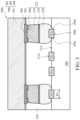
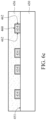
- FIG. 2 shows a partial cross section of another exemplary embodiment of a semiconductor package 500b of the invention. Elements of the embodiments that are the same or similar as those previously described with reference to FIG. 1 , are hereinafter not repeated for brevity.
- conductive traces 202b of the semiconductor package 500b embedded in the base 200 may have a top surface 212b designed to be aligned to a device attach surface 214 of the base 200 to improve routing ability for high-density semiconductor packages. That is to say, a bottom surface 206b and a sidewall 204b of the conductive trace 202b are designed to be fully connected to the base 200. Therefore, the solder cap 220 of the conductive structure 222 is disposed on the device attach surface 214 of the base 200, contacting the top surface 212b of the conductive trace 202b only.
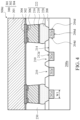
- FIG. 3 shows a partial cross section of yet another exemplary embodiment of a semiconductor package 500c of the invention. Elements of the embodiments that are the same or similar as those previously described with reference to FIGS. 1 and 2 , are hereinafter not repeated for brevity.
- conductive traces 202c of the semiconductor package 500c embedded in the base 200 may have a top surface 212c designed above a device attach surface 214 of the base 200 to improve routing ability for high-density semiconductor packages. That is to say, a bottom surface 206c and only a portion of a sidewall 204c of the conductive trace 202c are designed to be connected to the base 200. Therefore, the solder cap 220 of the conductive structure 222 is disposed on the device attach surface 214 of the base 200, wrapping a top surface 212c and only a portion of the sidewall 204c of the conductive trace 202C.
- FIG. 4 shows a partial cross section of still another exemplary embodiment of a semiconductor package sood of the invention. Elements of the embodiments that are the same or similar as those previously described with reference to FIGS. 1-3 , are hereinafter not repeated for brevity.
- the base may comprise a single layer structure as shown in FIGS. 1-3 .
- the base may comprise a multilayer structure.
- conductive traces 202d of the semiconductor package sood embedded in the base portion 200a may have a top surface 212d designed to be aligned to a surface 214 of the base portion 200a to improve routing ability for high-density semiconductor packages.
- a bottom surface 206d and a sidewall 204d of the conductive trace 202d are designed to be connected to the base portion 200a.
- an insulation layer 208 having openings 210 is disposed on the base portion 200a.
- the insulation layer 208 is disposed above the device attach surface 214 of the conductive trace 202d.
- the base portion 200a and the insulation layer 208 collectively serve as a multilayer base.
- the conductive traces 202d are exposed within the openings 210. Therefore, the solder cap 220 of the conductive structure 222 is formed through a portion of the insulation layer 208, contacting a top surface 212d of the conductive trace 202d only.
- the insulation layer 208 it is not necessary for the insulation layer 208 to align with the sidewall 204d of the conductive traces 202d. Instead, it can be designed to be distanced outward or inward from the sidewall 204d of the conductive traces 202d as shown in Fig. 4 .
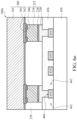
- FIGS. 5a to 5d are cross sections showing one exemplary embodiment of a method for fabricating two bases 200c and 200d for a semiconductor package of the invention.
- the method for fabricating bases for a semiconductor package is also called a double-sided base fabricating process.
- Elements of the embodiments that are the same or similar as those previously described with reference to FIGS. 1-4 are hereinafter not repeated for brevity.
- a carrier 400 with conductive seed layers 402a and 402b on a top surface 401 and a bottom surface 403 is provided.
- the carrier 400 may comprise FR4 glass epoxy or stainless steel.
- the conductive seed layers 402a and 402b are used as seed layers for subsequently formed interconnection conductive traces of bases on the top surface 401 and the bottom surface 403 of the carrier 400.
- the conductive seed layers 402a and 402b may comprise copper.
- first conductive traces 404a and 404b are respectively formed on the top surface 401 and the bottom surface 403 of the carrier 400. Bottom portions of the first conductive traces 404a and 404b connect to top portions of the conductive seed layers 402a and 402b.
- the first conductive traces 404a and 404b may be formed by a plating process and an anisotropic etching process. The plating process and the anisotropic etching process are simultaneously performed on the top surface 401 and the bottom surface 403 of the carrier 400.
- the plating process may comprise an electrical plating process.
- the first conductive traces 404a and 404b may comprise copper.
- the first conductive traces 404a and 404b are designed to have a width which is larger than 5 ⁇ m.
- the width of the conductive traces can be smaller than 5 ⁇ m if required.
- the anisotropic etching process may precisely control the width of the first conductive traces 404a and 404b.
- a laminating process is performed to respectively dispose a first base material layer 406a and a second base material layer 406b on the top surface 401 and the bottom surface 403 of the carrier 400, wherein the first base material layer 406a and a second base material layer 406b respectively cover the first conductive traces 404a and 404b.
- the laminating process of the first base material layer 406a and the second base material layer 406b is simultaneously performed on the on the top surface 401 and the bottom surface 403 of the carrier 400.
- the first base material layer 406a and the second base material layer 406b may comprise polypropylene (PP).
- a drilling process is performed to form openings (not shown) through the first base material layer 406a and the second base material layer 406b to define the formation positions of subsequently formed vias 408a and 408b.
- the drilling process may comprise a laser drilling process, an etching drilling process or a mechanical drilling process.
- a plating process is performed to fill a conductive material into the openings to form vias 408a and 408b for interconnecting the first conductive traces 404a and 404b to subsequent second conductive traces 410a and 410b.
- the drilling process and the plating process are simultaneously performed on the first base material layer 406a and the second base material layer 406b, respectively.
- FIG. 5c wherein a plurality of second conductive traces 410a and 410b are respectively formed on a first surface 412 of the first base material layer 406a and a first surface 414 of the second base material layer 406b.
- the first surface 412 of the first base material layer 406a and the first surface 414 of the second base material layer 406b are respectively away from the top surface 401 and the bottom surface 403 of the carrier 400.
- the second conductive traces 410a and 410b are formed by a plating process and an anisotropic etching process.
- the plating process and the anisotropic etching process are simultaneously performed on the first surface 412 of the first base material layer 406a and the first surface 414 of the second base material layer 406b.
- the plating process may comprise an electrical plating process.
- the second conductive traces 410a and 410b may comprise copper.
- the second conductive traces 410a and 410b are designed to have a width which is larger than 5 ⁇ m. However, it should be noted that there is no limitation on the width of the conductive traces. For different designs, the width of the conductive traces can be smaller than 5 ⁇ m if required.
- the anisotropic etching process may precisely control the width of the second conductive traces 410a and 410b.
- the first base material layer 406a with the first and second conductive traces 404a and 410a thereon and the second base material layer 406b with the first and second conductive traces 404b and 410b thereon are respectively separated from the top surface 401 and the bottom surface 403 of the carrier 400 to form a first base 200c and a second base 200d which are separated from each other.
- the conductive seed layers 402a and 402b are removed from the first base 200c and the second base 200d, respectively.
- the first conductive traces 404a and 404b are aligned to second surfaces 416 and 418 of the of the first and second bases 200c and 200d, which are respectively opposite to the first surfaces 412 and 414.
- the first base 200c and the second base 200d are simultaneously fabricated on opposite surfaces (the top surface 401 and the bottom surface 403) by the double-sided base fabricating process.
- two passivation or insulation layers having openings may be optionally formed respectively on a second surface 416 of the first base 200c and the second surface 418 of the second base 200d after the separation of the first base 200c and the second base 200d as shown in FIGS. 5d and 5e .
- the first conductive traces 404a and 404b of the first and second bases 200c and 200d are exposed within the opening. Positions of the insulation layer with openings and the first conductive traces 404a/404b as shown in FIG. 5d/5e can be similar to the insulation layer 208 with openings 210 and the conductive traces 202d as shown in FIG. 4 .
- the first base 200a/second base 200b and the insulation layer thereon collectively serve as a multilayer base.
- FIGS. 6a to 6e are cross sections showing another exemplary embodiment of a method for making a semiconductor package of the invention. Also, FIG. 6e shows a cross section of another exemplary embodiment of a semiconductor package 500e of the invention. Elements of the embodiments that are the same or similar as those previously described with reference to FIGS. 1-4 and 5a-5e , are hereinafter not repeated for brevity.
- the base may have a multilayer structure.
- a base 450 with a top surface 451 is provided.
- at least one conductive trace 454 is formed on the top surface 451 of the base 450.
- the conductive trace 454 may be formed by a plating process and an anisotropic etching process.
- the plating process may comprise an electrical plating process.
- the conductive trace 454 may comprise copper.
- the conductive trace 454 is designed to have a width which is larger than 5 ⁇ m. However, it should be noted that there is no limitation on the width of the conductive traces. For different designs, the width of the conductive traces can be smaller than 5 ⁇ m if required.
- the anisotropic etching process may precisely control the width of the conductive trace 454.
- a laminating process is performed to respectively dispose an additional insulation material 456 on the top surface 451 of the base 450. Also, the additional insulation material 456 covers a top surface 460 and sidewalls 462 of the conductive trace 454.
- a drilling process is performed to form at least one opening 458 through the additional insulation material 456 to define formation of a position of a subsequently formed conductive structure, for example, a copper bump structure or a solder bump structure.
- the drilling process may comprise a laser drilling process, an etching drilling process or a mechanical drilling process.
- the top surface 460 of the conductive trace 454 is exposed within the opening 458 of the additional insulation material 456.
- a bonding process is performed to mount a semiconductor device 300 on the base 450 through the conductive structure 222.
- the conductive structures 222 are disposed through the opening 458 of the additional insulation material 456, contacting to the top surface 460 of the conductive trace 454 only.
- an underfill material or the underfill 230 can be introduced into the gap between the semiconductor device 300 and the additional insulation material 456.
- the underfill 230 may comprises a capillary underfill (CUF), molded underfill (MUF) or a combination thereof.
- CCF capillary underfill
- UMF molded underfill
- the base 450, the additional insulation material 456, the semiconductor device 300, the conductive trace 454, and the conductive structure 222 collectively form a semiconductor package 500e.
- Exemplary embodiments provide a semiconductor package.
- the semiconductor package is designed to comprise conductive trace embedded in a base, for example, a print circuit board (PCB).
- the conductive traces may have a top surface disposed above, below or aligned to a surface of the base to improve routing ability for high-density semiconductor packages.
- the conductive traces are designed to have a width which is larger than 5 ⁇ m.
- the base may comprise a single layer structure or a multilayer structure.
- Exemplary embodiments also provide a method for fabricating a base for a semiconductor package. In one embodiment, the method can fabricate two bases on two sides of a carrier simultaneously. Also, the conductive traces may be embedded in the base.
- the conductive trace may be formed by a plating process and an anisotropic etching process, and the anisotropic etching process may precisely control the width of the conductive trace.
- the method can fabricate a base comprising a single layer structure or a multilayer structure to improve design capability.
Abstract
Description
- The present invention relates to a semiconductor package and a method for fabricating a base for a semiconductor package, and in particular, to a base for a high density semiconductor package.
- In order to ensure miniaturization and multi-functionality of electronic products or communication devices, semiconductor packages are desired to be small in size, to support multi-pin connection, to support high speeds, and to support high functionality. The demand for increasing Input-Output (I/O) pin counts and high-performance ICs has led to the development of flip chip packages.
- Flip-chip technology uses bumps on a chip to interconnect to a package substrate. The flip-chip is bonded face down to the package substrate through the shortest path. The technology used can be applied not only to a single-chip package, but also to higher or integrated levels of packaging in which the packages are larger and packaged with more sophisticated substrates that accommodate several chips to form larger functional units. The flip-chip technique, using an area array, can achieve a high density interconnection with devices and a very low inductance interconnection with packaging. However, this requires printed circuit board (PCB) fabricators to minimize line widths and space or to develop direct chip attach (DCA) semiconductors. Accordingly, the increased amount of input/output connections of a multifunctional flip-chip package may induce thermal electrical problems, for example, problems with heat dissipation, cross talk, signal propagation delay, electromagnetic interference for RF circuits, etc. The thermal electrical problems may affect the reliability and quality of products.
-
US 2010/0175917 A1 discloses a semiconductor device in which a chip is mounted on a wiring board. The chip is mounted on pads formed in a wiring layer of the wiring board by means of solder bumps. -
US 2008/0246146 A1 describes a semiconductor chip mounted on a support plate through an insulating layer by means of solder bumps made of solder and connected to underlying electrode pads having a layer structure including a gold layer and a layer and via conductive patterns formed in the insulating layer . - A semiconductor chip mounted on a built-up structure by means of solder bumps and metal bumps is know from
US 2011/0097850 A1 . - In
US 2006/121256 A1 , electrode pads are used for mounting a semiconductor device on a base. InUS 2009/079094 A1 , contact pads are employed on a carrier substrate for mounting a die on a PCB via solder bumps. -
US 2008/145967 A1 describes a plurality of package traces embedded in an insulating layer. This document discloses a trace layer with a bottom surface and sidewalls connected to an insulating layer and with top surface that is aligned with a surface of the insulating layer in which the solder is embedded. This same document also discloses a trace embedded in an insulating layer having a top surface below a surface of the insulating layer but without having a bottom surface fully connected to the insulating layer. -
US 2009/0250811 A1 describes a trace line having a top surface aligned with a surface of a surrounding substrate in which the trace line is embedded and trace lines that are not embedded in an underlying substrate. -
US 2011/013334 A1 likewise discloses a trace line having a top surface aligned with a surface of a surrounding substrate in which the trace line is embedded and trace lines that are not embedded in an underlying substrate. - None of
US 2008/0145967 A1 ,US 2009/0250811 A1 andUS 2011/013334 A1 discloses a conductive trace having a top surface above a surface of a base while being embedded in said base. -
US 7 589 398 B1 teaches using out-of-plane traces protruding from a base as screening elements for shielding adjacent in-plane traces embedded in the base. - Thus, a novel high-density flip chip package and a printed circuit board for a high-density flip chip package are desirable.
- A semiconductor package and a method for fabricating a base for a semiconductor package are provided. An exemplary embodiment of a semiconductor package includes a conductive trace embedded in a base. A semiconductor device is mounted on the conductive trace via a conductive structure.
- Another exemplary embodiment of a semiconductor package includes a conductive trace, having a bottom surface and at least a portion of a sidewall connected to a base. A semiconductor device is mounted on the conductive trace via a conductive structure.
- An exemplary embodiment of a method for fabricating a base for a semiconductor package includes providing a carrier with conductive seed layers on a top surface and a bottom surface of the carrier. First conductive traces are respectively formed on the top surface and the bottom surface of the carrier, connecting to the conductive seed layers. A first base material layer and a second base material layer are respectively laminated on the top surface and the bottom surface of the carrier, covering the first conductive traces. Second conductive traces are respectively formed on first surfaces of the first base material layer and the second base material layer, wherein the first surfaces of the first base material layer and the second base material layer are respectively away from the top surface and the bottom surface of the carrier. The first base material layer with the first and second conductive traces thereon and the second base material layer with the first and second conductive traces thereon are separated from the carrier to form a first base and a second base.
- Another exemplary embodiment of a method for fabricating a semiconductor package includes providing a base, forming a conductive trace on the base, further forming an additional insulation material on the base, and further defining patterns upon the additional insulation material, wherein the pattern is formed on at least one conductive trace.
- A detailed description is given in the following embodiments with reference to the accompanying drawings.
- The invention can be more fully understood by reading the subsequent detailed description and examples with references made to the accompanying drawings, wherein:
-
FIGS. 1 to 4 show cross sections of various exemplary embodiments of a semiconductor package of the invention. -
FIGS. 5a to 5e are cross sections showing one exemplary embodiment of a method for fabricating a base for a semiconductor package of the invention. -
FIGS. 6a to 6e are cross sections showing another exemplary embodiment of a method for fabricating a semiconductor package of the invention.. - The following description is a mode for carrying out the invention. This description is made for the purpose of illustrating the general principles of the invention and should not be taken in a limiting sense. The scope of the invention is best determined by reference to the appended claims. Wherever possible, the same reference numbers are used in the drawings and the descriptions to refer the same or like parts.
- The present invention will be described with respect to particular embodiments and with reference to certain drawings, but the invention is not limited thereto and is only limited by the claims. The drawings described are only schematic and are non-limiting. In the drawings, the size of some of the elements may be exaggerated and not drawn to scale for illustrative purposes. The dimensions and the relative dimensions do not correspond to actual dimensions to practice of the invention.
-
FIGS. 1 to 4 show cross sections of various exemplary embodiments of a semiconductor package of the invention. In this embodiment, the semiconductor package can be a flip chip package using conductive structures, for example, copper pillar bumps, connecting a semiconductor device to a base.. Alternatively, the semiconductor package can be a package using wire bonding technology to connect a semiconductor device to a base.FIG. 1 shows a partial cross section of one exemplary embodiment of asemiconductor package 500a of the invention. Please refer toFIG. 1 , wherein thesemiconductor package 500a comprises abase 200 having adevice attach surface 214. In one embodiment, thebase 200, for example, a print circuit board (PCB), may be formed of polypropylene (PP). It should be also noted that thebase 200 can be a single layer or a multilayer structure. A plurality ofconductive traces 202a is embedded in thebase 200. In one embodiment, theconductive traces 202a may comprise signal trace segments or ground trace segments, which are used for input/output (I/O) connections of asemiconductor device 300 mounted directly onto thebase 200. Therefore, each of theconductive traces 202a has a portion serving as a pad region of thebase 200. In this embodiment, theconductive traces 202a are designed to have a width which is larger than 5µm. However, it should be noted that there is no limitation on the width of the conductive traces. For different designs, the width of the conductive traces can be smaller than 5µm if required. - A
semiconductor device 300 is mounted on the device attachsurface 214 of the base 200 with an active surface of thesemiconductor device 300 facing the base 200 by a bonding process. In one embodiment, thesemiconductor device 300 may comprise a die, a passive component, a package or a wafer level package. In this embodiment, thesemiconductor device 300 is a flip chip package. A circuitry of thesemiconductor device 300 is disposed on the active surface, andmetal pads 304 are disposed on a top of the circuitry. The circuitry of thesemiconductor device 300 is interconnected to the circuitry of thebase 200 via a plurality ofconductive structures 222 disposed on the active surface of thesemiconductor device 300. However, it should be noted that theconductive structures 222 shown inFig.1 is only an example and is not a limitation to the present invention. - As shown in
FIG. 1 , thesemiconductor device 300 may include abody 301,metal pads 304 overlying thesemiconductor body 301, and aninsulation layer 302 covering themetal pads 304. In this embodiment, thesemiconductor body 301 may include but is not limited to a semiconductor substrate, circuit elements fabricated on the main surface of the semiconductor substrate, inter-layer dielectric (ILD) layers and an interconnection structure. In one embodiment, the interconnection structure may comprise a plurality of metal layers, a plurality of dielectric layers alternatively laminated with the metal layers and a plurality of vias formed through the dielectric layers on the semiconductor substrate. Themetal pads 304 comprise the topmost metal layer of the metal layers of the interconnection structure. In one embodiment, theinsulation layer 302 may be a single layer structure or a multilayer structure, and theinsulation layer 302 may comprise but is not limited to silicon nitride, silicon oxide, silicon oxynitride, polyimide or any combination thereof. Also, the theinsulation layer 302 may have functions of stress buffering and insulation. In one embodiment, themetal pad 304 may comprise but is not limited to aluminum, copper or alloys thereof. A plurality of openings can be formed in theinsulation layer 302. Each of the openings exposes at least a portion of one of themetal pads 304. - As shown in
FIG. 1 , theconductive structure 222 may comprise a conductive bump structure such as a copper bump or a solder bump structure, a conductive wire structure, or a conductive paste structure. In this embodiment, theconductive structure 222 may be a copper bump structure composed of a metal stack comprising a UBM (under bump metallurgy)layer 306, acopper layer 216 such as a plated copper layer, aconductive buffer layer 218, and asolder cap 220. In one embodiment, theUBM layer 306 can be formed on the exposedmetal pads 304 within the openings by a deposition method such as a sputtering or plating method and a subsequent anisotropic etching process. The anisotropic etching process is performed after forming conductive pillars. TheUBM layer 306 may also extend onto a top surface of theinsulation layer 302. In this embodiment, theUBM layer 306 may comprise titanium, copper or a combination thereof. Acopper layer 216 such as an electroplated copper layer can be formed on theUBM layer 306. The opening can be filled with thecopper layer 216 and theUBM layer 306, and thecopper layer 216 and theUBM layer 306 within the opening may form an integral plug of theconductive structure 222. A formation position of thecopper layer 216 is defined by a dry film photoresist or liquid photoresist patterns (not shown). - A
solder cap 220 can be formed on thecopper layer 216 by electroplating a solder with a patterned photoresist layer or by a screen printing process and a subsequent solder re-flow process. Aconductive buffer layer 218 formed of Ni may be formed between thecopper layer 216 and thesolder cap 220 by an electroplating method. Theconductive buffer layer 218 may serve as a seed layer, adhesion layer and barrier layer for thesolder cap 220 formed thereon. In this embodiment, theconductive structure 222, such as a conductive pillar structure, is used as a solder joint for themetal pad 304, which transmits input/output (I/O), ground or power signals of thesemiconductor device 300 formed thereon. Therefore, thecopper layer 216 of theconductive structure 222 may help to increase the mechanical strength of the bump structure. In one embodiment, an underfill material or theunderfill 230 can be introduced into the gap between thesemiconductor device 300 and thebase 200. In one embodiment, theunderfill 230 may comprises a capillary underfill (CUF), molded underfill (MUF) or a combination thereof. - In one embodiment, the conductive traces may have a top surface disposed above, below or aligned to a surface of the base to improve routing ability for high-density semiconductor packages. As shown in
FIG. 1 , theconductive traces 202a havetop surfaces 212a disposed below a device attachsurface 214 of thebase 200. That is to say, abottom surface 206a and at least a portion of asidewall 204a of theconductive trace 202a are designed to be connected to thebase 200. In this embodiment, thesolder cap 220 of theconductive structure 222 is disposed to contact with a portion of thebase 200 and to connect to atop surface 212a of theconductive trace 202a only. Due to the top surfaces of the conductive traces being recessed from the device attachsurface 214 of thebase 200, the bump-to-trace space is increased and the problem of bump-to-trace bridging can be effectively avoided. -
FIG. 2 shows a partial cross section of another exemplary embodiment of asemiconductor package 500b of the invention. Elements of the embodiments that are the same or similar as those previously described with reference toFIG. 1 , are hereinafter not repeated for brevity. In this embodiment,conductive traces 202b of thesemiconductor package 500b embedded in thebase 200 may have atop surface 212b designed to be aligned to a device attachsurface 214 of the base 200 to improve routing ability for high-density semiconductor packages. That is to say, abottom surface 206b and asidewall 204b of theconductive trace 202b are designed to be fully connected to thebase 200. Therefore, thesolder cap 220 of theconductive structure 222 is disposed on the device attachsurface 214 of thebase 200, contacting thetop surface 212b of theconductive trace 202b only. -
FIG. 3 shows a partial cross section of yet another exemplary embodiment of asemiconductor package 500c of the invention. Elements of the embodiments that are the same or similar as those previously described with reference toFIGS. 1 and2 , are hereinafter not repeated for brevity. In this embodiment,conductive traces 202c of thesemiconductor package 500c embedded in thebase 200 may have atop surface 212c designed above a device attachsurface 214 of the base 200 to improve routing ability for high-density semiconductor packages. That is to say, abottom surface 206c and only a portion of asidewall 204c of theconductive trace 202c are designed to be connected to thebase 200. Therefore, thesolder cap 220 of theconductive structure 222 is disposed on the device attachsurface 214 of thebase 200, wrapping atop surface 212c and only a portion of thesidewall 204c of the conductive trace 202C. -
FIG. 4 shows a partial cross section of still another exemplary embodiment of a semiconductor package sood of the invention. Elements of the embodiments that are the same or similar as those previously described with reference toFIGS. 1-3 , are hereinafter not repeated for brevity. In one embodiment, the base may comprise a single layer structure as shown inFIGS. 1-3 . Alternatively, the base may comprise a multilayer structure. In this embodiment,conductive traces 202d of the semiconductor package sood embedded in thebase portion 200a may have atop surface 212d designed to be aligned to asurface 214 of thebase portion 200a to improve routing ability for high-density semiconductor packages. That is to say, abottom surface 206d and asidewall 204d of theconductive trace 202d are designed to be connected to thebase portion 200a. Also, aninsulation layer 208 havingopenings 210 is disposed on thebase portion 200a. Theinsulation layer 208 is disposed above the device attachsurface 214 of theconductive trace 202d. In this embodiment, thebase portion 200a and theinsulation layer 208 collectively serve as a multilayer base. As shown inFIG. 4 , theconductive traces 202d are exposed within theopenings 210. Therefore, thesolder cap 220 of theconductive structure 222 is formed through a portion of theinsulation layer 208, contacting atop surface 212d of theconductive trace 202d only. It should be noted that it is not necessary for theinsulation layer 208 to align with thesidewall 204d of theconductive traces 202d. Instead, it can be designed to be distanced outward or inward from thesidewall 204d of theconductive traces 202d as shown inFig. 4 . -
FIGS. 5a to 5d are cross sections showing one exemplary embodiment of a method for fabricating twobases FIGS. 1-4 , are hereinafter not repeated for brevity. As shown inFIG. 5a , acarrier 400 withconductive seed layers top surface 401 and abottom surface 403 is provided. In one embodiment, thecarrier 400 may comprise FR4 glass epoxy or stainless steel. Also, theconductive seed layers top surface 401 and thebottom surface 403 of thecarrier 400. In one embodiment, theconductive seed layers - Next, as shown in
FIG. 5b , firstconductive traces top surface 401 and thebottom surface 403 of thecarrier 400. Bottom portions of the firstconductive traces conductive seed layers conductive traces top surface 401 and thebottom surface 403 of thecarrier 400. In one embodiment, the plating process may comprise an electrical plating process. In one embodiment, the firstconductive traces conductive traces conductive traces - Next, as shown in
FIG. 5c , a laminating process is performed to respectively dispose a firstbase material layer 406a and a secondbase material layer 406b on thetop surface 401 and thebottom surface 403 of thecarrier 400, wherein the firstbase material layer 406a and a secondbase material layer 406b respectively cover the firstconductive traces base material layer 406a and the secondbase material layer 406b is simultaneously performed on the on thetop surface 401 and thebottom surface 403 of thecarrier 400. In one embodiment, the firstbase material layer 406a and the secondbase material layer 406b may comprise polypropylene (PP). - Next, please refer to
FIG. 5c again, wherein a drilling process is performed to form openings (not shown) through the firstbase material layer 406a and the secondbase material layer 406b to define the formation positions of subsequently formedvias conductive traces conductive traces base material layer 406a and the secondbase material layer 406b, respectively. - Next, please refer to
FIG. 5c again, wherein a plurality of secondconductive traces first surface 412 of the firstbase material layer 406a and afirst surface 414 of the secondbase material layer 406b. As shown inFIG. 5c , thefirst surface 412 of the firstbase material layer 406a and thefirst surface 414 of the secondbase material layer 406b are respectively away from thetop surface 401 and thebottom surface 403 of thecarrier 400. The secondconductive traces first surface 412 of the firstbase material layer 406a and thefirst surface 414 of the secondbase material layer 406b. In one embodiment, the plating process may comprise an electrical plating process. In one embodiment, the secondconductive traces conductive traces conductive traces - Next, as shown in
FIG. 5d , the firstbase material layer 406a with the first and secondconductive traces base material layer 406b with the first and secondconductive traces top surface 401 and thebottom surface 403 of thecarrier 400 to form afirst base 200c and asecond base 200d which are separated from each other. Next, as shown inFIG. 5d again, theconductive seed layers first base 200c and thesecond base 200d, respectively. - As shown in
FIGS. 5d and 5e , the firstconductive traces second surfaces second bases first surfaces first base 200c and thesecond base 200d are simultaneously fabricated on opposite surfaces (thetop surface 401 and the bottom surface 403) by the double-sided base fabricating process. - Alternatively, two passivation or insulation layers (not shown) having openings may be optionally formed respectively on a
second surface 416 of thefirst base 200c and thesecond surface 418 of thesecond base 200d after the separation of thefirst base 200c and thesecond base 200d as shown inFIGS. 5d and 5e . In this embodiment, the firstconductive traces second bases conductive traces 404a/404b as shown inFIG. 5d/5e can be similar to theinsulation layer 208 withopenings 210 and theconductive traces 202d as shown inFIG. 4 . Also, in this embodiment, thefirst base 200a/second base 200b and the insulation layer thereon collectively serve as a multilayer base. -
FIGS. 6a to 6e are cross sections showing another exemplary embodiment of a method for making a semiconductor package of the invention. Also,FIG. 6e shows a cross section of another exemplary embodiment of asemiconductor package 500e of the invention. Elements of the embodiments that are the same or similar as those previously described with reference toFIGS. 1-4 and5a-5e , are hereinafter not repeated for brevity. Alternatively, the base may have a multilayer structure. As shown inFIG. 6a , a base 450 with atop surface 451 is provided. Next, as shown inFIG. 6b , at least oneconductive trace 454 is formed on thetop surface 451 of thebase 450. In one embodiment, theconductive trace 454 may be formed by a plating process and an anisotropic etching process. In one embodiment, the plating process may comprise an electrical plating process. In one embodiment, theconductive trace 454 may comprise copper. In one embodiment, theconductive trace 454 is designed to have a width which is larger than 5µm. However, it should be noted that there is no limitation on the width of the conductive traces. For different designs, the width of the conductive traces can be smaller than 5µm if required. In this embodiment, the anisotropic etching process may precisely control the width of theconductive trace 454. - Next, as shown in
FIG. 6c , a laminating process is performed to respectively dispose anadditional insulation material 456 on thetop surface 451 of thebase 450. Also, theadditional insulation material 456 covers atop surface 460 andsidewalls 462 of theconductive trace 454. - Next, please refer to
FIG. 6d , wherein a drilling process is performed to form at least oneopening 458 through theadditional insulation material 456 to define formation of a position of a subsequently formed conductive structure, for example, a copper bump structure or a solder bump structure. In one embodiment, the drilling process may comprise a laser drilling process, an etching drilling process or a mechanical drilling process. In this embodiment, thetop surface 460 of theconductive trace 454 is exposed within theopening 458 of theadditional insulation material 456. - Next, as shown in
FIG. 6e , a bonding process is performed to mount asemiconductor device 300 on the base 450 through theconductive structure 222. Elements of thesemiconductor device 300 and theconductive structure 222 that are the same or similar as those previously described with reference toFIGS. 1-4 , are hereinafter not repeated for brevity. After the bonding process, theconductive structures 222 are disposed through theopening 458 of theadditional insulation material 456, contacting to thetop surface 460 of theconductive trace 454 only. Next, an underfill material or theunderfill 230 can be introduced into the gap between thesemiconductor device 300 and theadditional insulation material 456. In one embodiment, theunderfill 230 may comprises a capillary underfill (CUF), molded underfill (MUF) or a combination thereof. Finally, thebase 450, theadditional insulation material 456, thesemiconductor device 300, theconductive trace 454, and theconductive structure 222 collectively form asemiconductor package 500e. - Exemplary embodiments provide a semiconductor package. The semiconductor package is designed to comprise conductive trace embedded in a base, for example, a print circuit board (PCB). The conductive traces may have a top surface disposed above, below or aligned to a surface of the base to improve routing ability for high-density semiconductor packages. Also, the conductive traces are designed to have a width which is larger than 5µm. Further, the base may comprise a single layer structure or a multilayer structure. Exemplary embodiments also provide a method for fabricating a base for a semiconductor package. In one embodiment, the method can fabricate two bases on two sides of a carrier simultaneously. Also, the conductive traces may be embedded in the base. Further, the conductive trace may be formed by a plating process and an anisotropic etching process, and the anisotropic etching process may precisely control the width of the conductive trace. Alternatively, the method can fabricate a base comprising a single layer structure or a multilayer structure to improve design capability.
- While the invention has been described by way of example and in terms of the preferred embodiments, it is to be understood that the invention is not limited to the disclosed embodiments. On the contrary, it is intended to cover various modifications and similar arrangements (as would be apparent to those skilled in the art). Therefore, the scope of the appended claims should be accorded the broadest interpretation so as to encompass all such modifications and similar arrangements.
- The present disclosure further refers to the following examples:
- 1. A semiconductor package, comprising:
- a conductive trace embedded in a base; and
- a semiconductor device mounted on the conductive trace via a conductive structure.
- 2. The semiconductor package of Example 1, wherein the conductive trace has a width which is larger than 5µm.
- 3. The semiconductor package of Example 1, wherein the conductive trace has a top surface above, below or aligned to a surface of the base.
- 4. The semiconductor package of Example 1, further comprising:
an underfill between the semiconductor device and the base. - 5. The semiconductor package of Example 3, further comprising:
an insulation layer having an opening disposed on the base, above the top surface of the conductive trace, wherein the conductive trace is exposed within the opening. - 6. The semiconductor package of Example 1, wherein the conductive structure contacts the conductive trace.
- 7. The semiconductor package of Example 1, wherein the conductive structure contacts a top surface of the conductive trace only.
- 8. The semiconductor package of Example 1, wherein the conductive structure wraps around a top surface and a portion of a sidewall of the conductive trace.
- 9. The semiconductor package of Example 1, wherein the conductive structure is connected to at least a portion of the base.
- 10. The semiconductor package of Example 1, wherein the conductive structure comprises a conductive pillar structure, a conductive wire structure, or a conductive paste structure.
- 11. The semiconductor package of Example 10, wherein the conductive pillar structure is composed of a metal stack comprising an under bump metallurgy (UBM) layer, a copper layer, and a solder cap.
- 12. The semiconductor package of Example 11, wherein the conductive pillar structure further comprises a conductive buffer layer between the copper layer and the solder cap.
- 13. The semiconductor package of Example 4, wherein the underfill comprises capillary underfill (CUF), molded underfill (MUF), nonconductive paste (NCP), nonconductive film (NCF) or a combination thereof.
- 14. The semiconductor package of Example 1, wherein the semiconductor device comprises a die, a passive component, a package or a wafer level package.
- 15. The semiconductor package of Example 1, wherein the conductive structure comprises a copper bump or solder bump structure.
- 16. The semiconductor package of Example 1, wherein the base comprises a single layer structure or a multilayer structure.
- 17. A semiconductor package, comprising:
- a conductive trace, having a bottom surface and at least a portion of a sidewall connected to a base; and
- a semiconductor device mounted on the conductive trace via a conductive structure.
- 18. A method for fabricating a base for a semiconductor package, comprising:
- providing a carrier with conductive seed layers on a top surface and a bottom surface of the carrier;
- forming first conductive traces respectively on the conductive seed layers;
- laminating a first base material layer and a second base material layer respectively on the conductive seed layers, covering the first conductive traces;
- forming second conductive traces respectively on first surfaces of the first base material layer and the second base material layer, wherein the first surfaces of the first base material layer and the second base material layer are respectively away from the top surface and the bottom surface of the carrier; and
- separating the first base material layer containing the first and second conductive traces thereon and the second base material layer containing the first and second conductive traces thereon from the carrier to form a first base and a second base.
- 19. The method for fabricating a base for a semiconductor package of Example 18, further comprising:
- performing a drilling process to form openings through the first base material layer and the second base material layer; and
- performing a plating process to fill a conductive material into the opening to form a via for interconnecting the first conductive traces to the second conductive traces, before forming the second conductive traces.
- 20. The method for fabricating a base for a semiconductor package of Example 19, wherein the drilling process comprises a laser drilling process, an etching drilling process or a mechanical drilling process, and the plating process comprises an electrical plating process.
- 21. The method for fabricating a base for a semiconductor package of Example 18, wherein the first conductive traces and the second conductive traces are formed by a plating process and an anisotropic etching process.
- 22. The method for fabricating a base for a semiconductor package of Example 18, further comprising:
removing conductive seed layers from the first base and the second base. - 23. The method for fabricating a base for a semiconductor package of Example 18, further comprising:
forming insulation layers having openings respectively on the first and second bases, wherein the first conductive traces of the first and second bases are exposed within the openings. - 24. The method for fabricating a base for a semiconductor package of Example 18, wherein the first conductive traces of the first and second bases are aligned to second surfaces of the of the first and second bases, and wherein the second surfaces are respectively opposite to the first surfaces of the first and second bases.
- 25. The method for fabricating a base for a semiconductor package of Example 18, wherein the first conductive traces have a width which is larger than 5µm.
- 26. A method for fabricating a semiconductor package, comprising:
- providing a base;
- forming at least one conductive trace on the base;
- forming an additional insulation material on the base; and
- defining patterns upon the additional insulation material, wherein the pattern is formed on at least one conductive trace.
- 27. A semiconductor package, comprising:
- a conductive trace embedded in a base; and
- a semiconductor device mounted on the conductive trace via a conductive structure.
- 28. The semiconductor package of Example 27, wherein the conductive trace has a width which is larger than 5µm.
- 29. The semiconductor package of Example 27 or 28, wherein the conductive trace has a top surface above, below or aligned to a surface of the base.
- 30. The semiconductor package of any of Examples 27-29, further comprising:
an insulation layer having an opening disposed on the base, above the top surface of the conductive trace, wherein the conductive trace is exposed within the opening. - 31. The semiconductor package of any of Examples 27-30, wherein the conductive structure contacts the conductive trace;
wherein the conductive structure preferably contacts a top surface of the conductive trace only. - 32. The semiconductor package of any of Examples 27-31, wherein the conductive structure wraps around a top surface and a portion of a sidewall of the conductive trace.
- 33. The semiconductor package of any of Examples 27-32, wherein the conductive structure is connected to at least a portion of the base.
- 34. The semiconductor package of any of Examples 27-33, wherein the conductive structure comprises a conductive pillar structure, a conductive wire structure, or a conductive paste structure, wherein the conductive pillar structure is preferably composed of a metal stack comprising an under bump metallurgy (UBM) layer, a copper layer, and a solder cap, and in particular wherein the conductive pillar structure further comprises a conductive buffer layer between the copper layer and the solder cap.
- 35. The semiconductor package of any of the preceding claims 27-34, wherein
the conductive trace has a bottom surface and at least a portion of a sidewall connected to the base, wherein the bottom surface and the at least a portion of the sidewall preferably are fully connected to the base. - 36. The semiconductor package of Example 35, wherein the conductive structure comprises a solder cap in contact with a top surface of the conductive trace, and wherein a top surface of the conductive trace is below a surface of the base.
- 37. The semiconductor package of any of Examples 27-36, wherein
the conductive trace has a bottom surface and at least a portion of a sidewall fully connected to the base, wherein the base is a printed circuit board. - 38. The semiconductor package of any of Examples 27-37, wherein
the conductive trace is formed by a plating process and an anisotropic etching process. - 39. The semiconductor package of any of Examples 27-38, wherein the conductive trace comprises a signal trace segment or ground trace segment for carrying signals of input/output connections of the semiconductor device.
- 40. The semiconductor package of any of Examples 27-39, wherein the conductive trace comprises a portion configured as a pad region of the base, and wherein the semiconductor device is mounted on the conductive trace via the conductive structure and the pad region.
- 41. The semiconductor package of any of Examples 27-40, wherein the conductive trace comprises copper.
Claims (15)
- A semiconductor package comprising:
one or more conductive traces (202a; 202b; 202c; 202d) embedded in a base (200); and a semiconductor device (300) mounted on the one or more conductive traces (202a; 202b; 202c; 202d) via a conductive structure (222). - The semiconductor package as claimed in claim 1, wherein the conductive trace has a width which is larger than 5 µm.
- The semiconductor package as claimed in claim 1 or 2, further comprising:
an underfill between the semiconductor device and the base. - The semiconductor package as claimed in any of the preceding claims, wherein the one or more conductive traces (202a; 202b; 202c; 202d) comprise signal trace segments or ground trace segments for carrying signals of input/output connections of the semiconductor device (300).
- The semiconductor package as claimed in any of the preceding claims, wherein each of the one or more conductive traces (202a; 202b; 202c; 202d) comprises a portion configured as a pad region of the base (200), and wherein the semiconductor device (300) is mounted on the one or more conductive traces (202a; 202b; 202c; 202d) via the conductive structure (222) and the pad regions.
- The semiconductor package as claimed in any of the preceding claims, wherein the conductive structure (222) comprises a conductive pillar structure having a copper layer and a solder cap.
- The semiconductor package as claimed in claim 6, wherein the conductive pillar structure further comprises a metal stack comprising an under bump metallurgy (UBM) layer, the copper layer, and the solder cap.
- The semiconductor package as claimed in claim 7, wherein the conductive pillar structure further comprises a conductive buffer layer between the copper layer and the solder cap.
- The semiconductor package of any of the preceding claims, wherein
a bottom surface (206a; 2026; 2026; 2026) and at least a portion of a sidewall (204a; 204b; 204c; 204d) of each of the one or more conductive traces (202a; 202b; 202c; 202d) is connected to the base (200). - The semiconductor package as claimed in any of the preceding claims, wherein the conductive structure (222) contacts a top surface (212a; 212b; 212c; 212d) of the one or more conductive traces (202a; 202b; 202c; 202d) and at least a portion of the base (200).
- The semiconductor package as claimed in any of the preceding claims, wherein the one or more conductive traces (202a; 202b; 202d) have a top surface (212a; 212b; 212d) below or aligned to a surface (214) of the base (200).
- The semiconductor package of any of the preceding claims, wherein the conductive structure (222) laterally extends beyond a respective one of the conductive traces (202a; 202b; 202C; 202d).
- The semiconductor package of any of the preceding claims, wherein the conductive structure (222) contacts a top surface (212a; 212b; 212c; 212d) of the one or more conductive traces (202a; 202b; 202c; 202d) over an entire width (W1) thereof.
- The semiconductor package of any of the preceding claims, wherein the one or more conductive traces (202a) have a top surface (212a) below a device attach surface (214) of the base (200) and wherein the conductive structure (222) contacts with a portion of the base (200) and with a top surface (212a) of the one or more conductive traces (202a).
- The semiconductor package of any of the preceding claims, wherein each conductive trace is formed as a single layer.
Applications Claiming Priority (4)
| Application Number | Priority Date | Filing Date | Title |
|---|---|---|---|
| US13/721,983 US9177899B2 (en) | 2012-07-31 | 2012-12-20 | Semiconductor package and method for fabricating base for semiconductor package |
| EP20209680.6A EP3800664B1 (en) | 2012-12-20 | 2013-12-19 | Semiconductor package and method for fabricating base for semiconductor package |
| EP13863897.8A EP2936558B1 (en) | 2012-12-20 | 2013-12-19 | Method for fabricating base for semiconductor package |
| PCT/CN2013/089940 WO2014094629A1 (en) | 2012-12-20 | 2013-12-19 | Semiconductor package and method for fabricating base for semiconductor package |
Related Parent Applications (2)
| Application Number | Title | Priority Date | Filing Date |
|---|---|---|---|
| EP13863897.8A Division EP2936558B1 (en) | 2012-12-20 | 2013-12-19 | Method for fabricating base for semiconductor package |
| EP20209680.6A Division EP3800664B1 (en) | 2012-12-20 | 2013-12-19 | Semiconductor package and method for fabricating base for semiconductor package |
Publications (2)
| Publication Number | Publication Date |
|---|---|
| EP4235762A2 true EP4235762A2 (en) | 2023-08-30 |
| EP4235762A3 EP4235762A3 (en) | 2023-09-20 |
Family
ID=50979426
Family Applications (3)
| Application Number | Title | Priority Date | Filing Date |
|---|---|---|---|
| EP13863897.8A Active EP2936558B1 (en) | 2012-12-20 | 2013-12-19 | Method for fabricating base for semiconductor package |
| EP20209680.6A Active EP3800664B1 (en) | 2012-12-20 | 2013-12-19 | Semiconductor package and method for fabricating base for semiconductor package |
| EP23173505.1A Pending EP4235762A3 (en) | 2012-12-20 | 2013-12-19 | Semiconductor package and method for fabricating base for semiconductor package |
Family Applications Before (2)
| Application Number | Title | Priority Date | Filing Date |
|---|---|---|---|
| EP13863897.8A Active EP2936558B1 (en) | 2012-12-20 | 2013-12-19 | Method for fabricating base for semiconductor package |
| EP20209680.6A Active EP3800664B1 (en) | 2012-12-20 | 2013-12-19 | Semiconductor package and method for fabricating base for semiconductor package |
Country Status (4)
| Country | Link |
|---|---|
| US (1) | US9177899B2 (en) |
| EP (3) | EP2936558B1 (en) |
| KR (2) | KR101731198B1 (en) |
| WO (1) | WO2014094629A1 (en) |
Families Citing this family (20)
| Publication number | Priority date | Publication date | Assignee | Title |
|---|---|---|---|---|
| US10991669B2 (en) | 2012-07-31 | 2021-04-27 | Mediatek Inc. | Semiconductor package using flip-chip technology |
| TWI562295B (en) | 2012-07-31 | 2016-12-11 | Mediatek Inc | Semiconductor package and method for fabricating base for semiconductor package |
| US8802556B2 (en) * | 2012-11-14 | 2014-08-12 | Qualcomm Incorporated | Barrier layer on bump and non-wettable coating on trace |
| US9536833B2 (en) | 2013-02-01 | 2017-01-03 | Mediatek Inc. | Semiconductor device allowing metal layer routing formed directly under metal pad |
| US9455226B2 (en) | 2013-02-01 | 2016-09-27 | Mediatek Inc. | Semiconductor device allowing metal layer routing formed directly under metal pad |
| US9418928B2 (en) | 2014-01-06 | 2016-08-16 | Taiwan Semiconductor Manufacturing Company, Ltd. | Protrusion bump pads for bond-on-trace processing |
| US9275967B2 (en) | 2014-01-06 | 2016-03-01 | Taiwan Semiconductor Manufacturing Company, Ltd. | Protrusion bump pads for bond-on-trace processing |
| US9508637B2 (en) | 2014-01-06 | 2016-11-29 | Taiwan Semiconductor Manufacturing Company, Ltd. | Protrusion bump pads for bond-on-trace processing |
| US9305890B2 (en) * | 2014-01-15 | 2016-04-05 | Taiwan Semiconductor Manufacturing Company, Ltd. | Package having substrate with embedded metal trace overlapped by landing pad |
| DE102014105989A1 (en) * | 2014-04-29 | 2015-10-29 | Gako International Gmbh | Pharmacy Recipe Making System and Pharmacy Recipe Making Process for Preparing Individual Pharmaceutical Formulas |
| US9502267B1 (en) | 2014-06-26 | 2016-11-22 | STATS ChipPAC Pte. Ltd. | Integrated circuit packaging system with support structure and method of manufacture thereof |
| US9412624B1 (en) | 2014-06-26 | 2016-08-09 | STATS ChipPAC Pte. Ltd. | Integrated circuit packaging system with substrate and method of manufacture thereof |
| US20160064340A1 (en) * | 2014-08-28 | 2016-03-03 | Taiwan Semiconductor Manufacturing Company Ltd. | Semiconductor device and manufacturing method thereof |
| TWI585923B (en) * | 2014-10-03 | 2017-06-01 | 矽品精密工業股份有限公司 | Package substrate, package structure and method of manufacture |
| DE102016108060B4 (en) * | 2016-04-29 | 2020-08-13 | Infineon Technologies Ag | Chip Carrier Packages With Void Based Feature And Process For Their Manufacture |
| DE102017102035A1 (en) * | 2017-02-02 | 2018-08-02 | Infineon Technologies Ag | A semiconductor device, method of manufacturing a semiconductor device, and method of amplifying a die in a semiconductor device |
| CN110581075B (en) * | 2018-06-08 | 2021-11-02 | 欣兴电子股份有限公司 | Circuit carrier plate structure and manufacturing method thereof |
| US10879158B2 (en) * | 2019-05-29 | 2020-12-29 | Qualcomm Incorporated | Split conductive pad for device terminal |
| DE102019127924B3 (en) * | 2019-10-16 | 2021-01-21 | Tdk Electronics Ag | Component and method for manufacturing a component |
| US11682607B2 (en) * | 2021-02-01 | 2023-06-20 | Qualcomm Incorporated | Package having a substrate comprising surface interconnects aligned with a surface of the substrate |
Citations (6)
| Publication number | Priority date | Publication date | Assignee | Title |
|---|---|---|---|---|
| US20080246146A1 (en) | 2007-04-04 | 2008-10-09 | Shinko Electric Industries Co., Ltd. | Wiring substrate and wiring substrate manufacturing method |
| US20090079094A1 (en) | 2007-09-21 | 2009-03-26 | Stats Chippac, Ltd. | Solder Bump with Inner Core Pillar in Semiconductor Package |
| US20090250811A1 (en) | 2004-11-10 | 2009-10-08 | Stats Chippac, Ltd. | Semiconductor Device and Method of Self-Confinement of Conductive Bump Material During Reflow Without Solder Mask |
| US20100175917A1 (en) | 2009-01-15 | 2010-07-15 | Shinko Electric Industries Co., Ltd. | Wiring board and method of manufacturing the same |
| US20110013334A1 (en) | 2008-01-31 | 2011-01-20 | Peter Bobert | Electrical Protection Component with a Short-Circuiting Device |
| US20110097850A1 (en) | 2009-10-22 | 2011-04-28 | Unimicron Technology Corporation | Method of fabricating a packaging structure |
Family Cites Families (48)
| Publication number | Priority date | Publication date | Assignee | Title |
|---|---|---|---|---|
| JP2715793B2 (en) * | 1992-03-19 | 1998-02-18 | 日本電気株式会社 | Semiconductor device and manufacturing method thereof |
| US5895229A (en) | 1997-05-19 | 1999-04-20 | Motorola, Inc. | Microelectronic package including a polymer encapsulated die, and method for forming same |
| US20020105789A1 (en) | 2001-02-02 | 2002-08-08 | Siliconware Precision Industries Co., Ltd. | Semiconductor package for multi-chip stacks |
| US6510976B2 (en) | 2001-05-18 | 2003-01-28 | Advanpack Solutions Pte. Ltd. | Method for forming a flip chip semiconductor package |
| US6550666B2 (en) | 2001-08-21 | 2003-04-22 | Advanpack Solutions Pte Ltd | Method for forming a flip chip on leadframe semiconductor package |
| KR100636259B1 (en) * | 2001-12-07 | 2006-10-19 | 후지쯔 가부시끼가이샤 | Semiconductor device and method for manufacturing the same |
| JP2003303842A (en) | 2002-04-12 | 2003-10-24 | Nec Electronics Corp | Semiconductor device and manufacturing method therefor |
| US6734039B2 (en) | 2002-09-06 | 2004-05-11 | Advanpack Solutions Pte Ltd. | Semiconductor chip grid array package design and method of manufacture |
| US6929981B2 (en) | 2002-09-06 | 2005-08-16 | Advanpack Solutions Pte, Ltd. | Package design and method of manufacture for chip grid array |
| US6750082B2 (en) | 2002-09-13 | 2004-06-15 | Advanpack Solutions Pte. Ltd. | Method of assembling a package with an exposed die backside with and without a heatsink for flip-chip |
| US20040108580A1 (en) | 2002-12-09 | 2004-06-10 | Advanpack Solutions Pte. Ltd. | Leadless semiconductor packaging structure with inverted flip chip and methods of manufacture |
| US7320173B2 (en) * | 2003-02-06 | 2008-01-22 | Lg Electronics Inc. | Method for interconnecting multi-layer printed circuit board |
| US7462942B2 (en) | 2003-10-09 | 2008-12-09 | Advanpack Solutions Pte Ltd | Die pillar structures and a method of their formation |
| US20050087883A1 (en) | 2003-10-22 | 2005-04-28 | Advanpack Solutions Pte. Ltd. | Flip chip package using no-flow underfill and method of fabrication |
| TWI478254B (en) * | 2003-11-10 | 2015-03-21 | Chippac Inc | Bump-on-lead flip chip interconnection |
| US20060060937A1 (en) | 2004-09-23 | 2006-03-23 | Advanpack Solutions Pte Ltd | Embedded passive component |
| US20060103016A1 (en) | 2004-11-12 | 2006-05-18 | Advanpack Solutions Pte Ltd | Heat sinking structure |
| KR100674319B1 (en) | 2004-12-02 | 2007-01-24 | 삼성전기주식회사 | Manufacturing method of printed circuit board having thin core layer |
| JP4768994B2 (en) | 2005-02-07 | 2011-09-07 | ルネサスエレクトロニクス株式会社 | Wiring board and semiconductor device |
| US20060180888A1 (en) | 2005-02-14 | 2006-08-17 | Advanpack Solutions Pte Ltd | Optical sensor package and method of manufacture |
| US8148822B2 (en) | 2005-07-29 | 2012-04-03 | Megica Corporation | Bonding pad on IC substrate and method for making the same |
| US20070196979A1 (en) | 2006-02-21 | 2007-08-23 | Advanpack Solutions Pte Ltd | Flip chip in package using flexible and removable leadframe |
| US20070284420A1 (en) | 2006-06-13 | 2007-12-13 | Advanpack Solutions Pte Ltd | Integrated circuit chip formed on substrate |
| JP5117692B2 (en) * | 2006-07-14 | 2013-01-16 | ルネサスエレクトロニクス株式会社 | Manufacturing method of semiconductor device |
| US7589398B1 (en) * | 2006-10-04 | 2009-09-15 | Amkor Technology, Inc. | Embedded metal features structure |
| TWI378540B (en) | 2006-10-14 | 2012-12-01 | Advanpack Solutions Pte Ltd | Chip and manufacturing method thereof |
| DE102007034402B4 (en) | 2006-12-14 | 2014-06-18 | Advanpack Solutions Pte. Ltd. | Semiconductor package and manufacturing method therefor |
| TW200828477A (en) | 2006-12-22 | 2008-07-01 | Advanpack Solutions Pte Ltd | Device and method for testing semiconductor element, and manufacturing method thereof |
| US20080248610A1 (en) | 2007-04-03 | 2008-10-09 | Advanpack Solutions Pte Ltd | Thermal bonding process for chip packaging |
| US7939939B1 (en) | 2007-06-11 | 2011-05-10 | Texas Instruments Incorporated | Stable gold bump solder connections |
| TWI357137B (en) | 2007-10-19 | 2012-01-21 | Advanced Semiconductor Eng | Flip chip package structure and carrier thereof |
| US7880297B2 (en) | 2007-12-31 | 2011-02-01 | Mediatek Inc. | Semiconductor chip having conductive member for reducing localized voltage drop |
| TWI425896B (en) * | 2008-06-11 | 2014-02-01 | Advanced Semiconductor Eng | Circuit board with buried conductive trace formed thereon and method for manufacturing the same |
| US20100073894A1 (en) * | 2008-09-22 | 2010-03-25 | Russell Mortensen | Coreless substrate, method of manufacturing same, and package for microelectronic device incorporating same |
| US8659172B2 (en) * | 2008-12-31 | 2014-02-25 | Stats Chippac, Ltd. | Semiconductor device and method of confining conductive bump material with solder mask patch |
| TW201133745A (en) | 2009-08-27 | 2011-10-01 | Advanpack Solutions Private Ltd | Stacked bump interconnection structure and semiconductor package formed using the same |
| US9607936B2 (en) | 2009-10-29 | 2017-03-28 | Taiwan Semiconductor Manufacturing Company, Ltd. | Copper bump joint structures with improved crack resistance |
| JP5603600B2 (en) | 2010-01-13 | 2014-10-08 | 新光電気工業株式会社 | WIRING BOARD, MANUFACTURING METHOD THEREOF, AND SEMICONDUCTOR PACKAGE |
| CN202275822U (en) | 2010-04-28 | 2012-06-13 | 先进封装技术私人有限公司 | Semiconductor encapsulation piece and its substrate |
| TWI543327B (en) | 2010-08-31 | 2016-07-21 | 先進封裝技術私人有限公司 | Semiconductor device carrier |
| US20120267779A1 (en) | 2011-04-25 | 2012-10-25 | Mediatek Inc. | Semiconductor package |
| US8288871B1 (en) * | 2011-04-27 | 2012-10-16 | Taiwan Semiconductor Manufacturing Company, Ltd. | Reduced-stress bump-on-trace (BOT) structures |
| TWI601250B (en) | 2011-07-22 | 2017-10-01 | 先進封裝技術私人有限公司 | Semiconductor substrate for making semiconductor package device and manufacturing method thereof |
| US9053989B2 (en) | 2011-09-08 | 2015-06-09 | Taiwan Semiconductor Manufacturing Company, Ltd. | Elongated bump structure in semiconductor device |
| US9536818B2 (en) | 2011-10-13 | 2017-01-03 | Taiwan Semiconductor Manufacturing Company, Ltd. | Semiconductor package and method of forming the same |
| CN103066051B (en) | 2011-10-20 | 2017-03-01 | 先进封装技术私人有限公司 | Base plate for packaging and its processing technology, semiconductor component packaging structure and processing technology |
| TWI500124B (en) | 2011-11-29 | 2015-09-11 | Advanpack Solutions Pte Ltd | Substrate structure, semiconductor package device, and manufacturing method of substrate structure |
| US9723717B2 (en) | 2011-12-19 | 2017-08-01 | Advanpack Solutions Pte Ltd. | Substrate structure, semiconductor package device, and manufacturing method of semiconductor package |
-
2012
- 2012-12-20 US US13/721,983 patent/US9177899B2/en active Active
-
2013
- 2013-12-19 EP EP13863897.8A patent/EP2936558B1/en active Active
- 2013-12-19 WO PCT/CN2013/089940 patent/WO2014094629A1/en active Application Filing
- 2013-12-19 KR KR1020157019713A patent/KR101731198B1/en active IP Right Grant
- 2013-12-19 KR KR1020177010496A patent/KR101849057B1/en active IP Right Grant
- 2013-12-19 EP EP20209680.6A patent/EP3800664B1/en active Active
- 2013-12-19 EP EP23173505.1A patent/EP4235762A3/en active Pending
Patent Citations (6)
| Publication number | Priority date | Publication date | Assignee | Title |
|---|---|---|---|---|
| US20090250811A1 (en) | 2004-11-10 | 2009-10-08 | Stats Chippac, Ltd. | Semiconductor Device and Method of Self-Confinement of Conductive Bump Material During Reflow Without Solder Mask |
| US20080246146A1 (en) | 2007-04-04 | 2008-10-09 | Shinko Electric Industries Co., Ltd. | Wiring substrate and wiring substrate manufacturing method |
| US20090079094A1 (en) | 2007-09-21 | 2009-03-26 | Stats Chippac, Ltd. | Solder Bump with Inner Core Pillar in Semiconductor Package |
| US20110013334A1 (en) | 2008-01-31 | 2011-01-20 | Peter Bobert | Electrical Protection Component with a Short-Circuiting Device |
| US20100175917A1 (en) | 2009-01-15 | 2010-07-15 | Shinko Electric Industries Co., Ltd. | Wiring board and method of manufacturing the same |
| US20110097850A1 (en) | 2009-10-22 | 2011-04-28 | Unimicron Technology Corporation | Method of fabricating a packaging structure |
Also Published As
| Publication number | Publication date |
|---|---|
| EP2936558A4 (en) | 2016-08-31 |
| EP4235762A3 (en) | 2023-09-20 |
| EP3800664A1 (en) | 2021-04-07 |
| EP3800664B1 (en) | 2023-05-17 |
| KR101731198B1 (en) | 2017-04-27 |
| KR20150099820A (en) | 2015-09-01 |
| US9177899B2 (en) | 2015-11-03 |
| US20140035095A1 (en) | 2014-02-06 |
| KR20170046188A (en) | 2017-04-28 |
| KR101849057B1 (en) | 2018-04-13 |
| EP2936558A1 (en) | 2015-10-28 |
| WO2014094629A1 (en) | 2014-06-26 |
| EP2936558B1 (en) | 2021-02-03 |
Similar Documents
| Publication | Publication Date | Title |
|---|---|---|
| US11469201B2 (en) | Semiconductor package and method for fabricating base for semiconductor package | |
| EP2936558B1 (en) | Method for fabricating base for semiconductor package | |
| US10109608B2 (en) | Semiconductor package | |
| US6982487B2 (en) | Wafer level package and multi-package stack | |
| WO2005059998A1 (en) | Integrated circuits and packaging substrates with cavities, and attachment methods including insertion of protruding contact pads into cavities | |
| EP2107599B1 (en) | Method Of Forming A Wafer Level Package | |
| EP2919265B1 (en) | Semiconductor package and its manufacturing method | |
| US20210202425A1 (en) | Semiconductor package using flip-chip technology | |
| KR20180069368A (en) | Method for forming bump of semiconductor package | |
| TWI599008B (en) | Semiconductor package | |
| JP2011142185A (en) | Semiconductor device | |
| TWI740219B (en) | Carrier and manufacturing method thereof | |
| US7410824B2 (en) | Method for solder bumping, and solder-bumping structures produced thereby | |
| US9265147B2 (en) | Multi-layer wiring board | |
| US20120211257A1 (en) | Pyramid bump structure | |
| TWI543311B (en) | Method for fabricating base for semiconductor package | |
| KR20050027384A (en) | Chip size package having rerouting pad and stack thereof |
Legal Events
| Date | Code | Title | Description |
|---|---|---|---|
| PUAI | Public reference made under article 153(3) epc to a published international application that has entered the european phase |
Free format text: ORIGINAL CODE: 0009012 |
|
| STAA | Information on the status of an ep patent application or granted ep patent |
Free format text: STATUS: THE APPLICATION HAS BEEN PUBLISHED |
|
| REG | Reference to a national code |
Ref country code: DE Ref legal event code: R079 Free format text: PREVIOUS MAIN CLASS: H01L0021683000 Ipc: H01L0025000000 |
|
| PUAL | Search report despatched |
Free format text: ORIGINAL CODE: 0009013 |
|
| AC | Divisional application: reference to earlier application |
Ref document number: 2936558 Country of ref document: EP Kind code of ref document: P Ref document number: 3800664 Country of ref document: EP Kind code of ref document: P |
|
| AK | Designated contracting states |
Kind code of ref document: A2 Designated state(s): AL AT BE BG CH CY CZ DE DK EE ES FI FR GB GR HR HU IE IS IT LI LT LU LV MC MK MT NL NO PL PT RO RS SE SI SK SM TR |
|
| AK | Designated contracting states |
Kind code of ref document: A3 Designated state(s): AL AT BE BG CH CY CZ DE DK EE ES FI FR GB GR HR HU IE IS IT LI LT LU LV MC MK MT NL NO PL PT RO RS SE SI SK SM TR |
|
| RIC1 | Information provided on ipc code assigned before grant |
Ipc: H01L 21/683 20060101ALI20230814BHEP Ipc: H01L 21/48 20060101ALI20230814BHEP Ipc: H01L 23/498 20060101ALI20230814BHEP Ipc: H01L 23/48 20060101ALI20230814BHEP Ipc: H01L 25/00 20060101AFI20230814BHEP |
|
| STAA | Information on the status of an ep patent application or granted ep patent |
Free format text: STATUS: REQUEST FOR EXAMINATION WAS MADE |