EP4235467B1 - Elektronische vorrichtung mit einem zwischen einer anzeigetafel und einem ultraschallsensor angeordneten, lichtabsorbierenden element - Google Patents
Elektronische vorrichtung mit einem zwischen einer anzeigetafel und einem ultraschallsensor angeordneten, lichtabsorbierenden element Download PDFInfo
- Publication number
- EP4235467B1 EP4235467B1 EP23177546.1A EP23177546A EP4235467B1 EP 4235467 B1 EP4235467 B1 EP 4235467B1 EP 23177546 A EP23177546 A EP 23177546A EP 4235467 B1 EP4235467 B1 EP 4235467B1
- Authority
- EP
- European Patent Office
- Prior art keywords
- electronic device
- adhesive layer
- ultrasonic wave
- display panel
- absorbing member
- Prior art date
- Legal status (The legal status is an assumption and is not a legal conclusion. Google has not performed a legal analysis and makes no representation as to the accuracy of the status listed.)
- Active
Links
Images















Classifications
-
- G—PHYSICS
- G06—COMPUTING OR CALCULATING; COUNTING
- G06F—ELECTRIC DIGITAL DATA PROCESSING
- G06F1/00—Details not covered by groups G06F3/00 - G06F13/00 and G06F21/00
- G06F1/16—Constructional details or arrangements
- G06F1/1613—Constructional details or arrangements for portable computers
- G06F1/1626—Constructional details or arrangements for portable computers with a single-body enclosure integrating a flat display, e.g. Personal Digital Assistants [PDAs]
-
- G—PHYSICS
- G06—COMPUTING OR CALCULATING; COUNTING
- G06F—ELECTRIC DIGITAL DATA PROCESSING
- G06F3/00—Input arrangements for transferring data to be processed into a form capable of being handled by the computer; Output arrangements for transferring data from processing unit to output unit, e.g. interface arrangements
- G06F3/01—Input arrangements or combined input and output arrangements for interaction between user and computer
- G06F3/03—Arrangements for converting the position or the displacement of a member into a coded form
- G06F3/041—Digitisers, e.g. for touch screens or touch pads, characterised by the transducing means
- G06F3/0416—Control or interface arrangements specially adapted for digitisers
-
- G—PHYSICS
- G06—COMPUTING OR CALCULATING; COUNTING
- G06F—ELECTRIC DIGITAL DATA PROCESSING
- G06F1/00—Details not covered by groups G06F3/00 - G06F13/00 and G06F21/00
- G06F1/16—Constructional details or arrangements
- G06F1/1613—Constructional details or arrangements for portable computers
- G06F1/1633—Constructional details or arrangements of portable computers not specific to the type of enclosures covered by groups G06F1/1615 - G06F1/1626
- G06F1/1637—Details related to the display arrangement, including those related to the mounting of the display in the housing
-
- G—PHYSICS
- G06—COMPUTING OR CALCULATING; COUNTING
- G06F—ELECTRIC DIGITAL DATA PROCESSING
- G06F21/00—Security arrangements for protecting computers, components thereof, programs or data against unauthorised activity
- G06F21/30—Authentication, i.e. establishing the identity or authorisation of security principals
- G06F21/31—User authentication
- G06F21/32—User authentication using biometric data, e.g. fingerprints, iris scans or voiceprints
-
- G—PHYSICS
- G06—COMPUTING OR CALCULATING; COUNTING
- G06F—ELECTRIC DIGITAL DATA PROCESSING
- G06F3/00—Input arrangements for transferring data to be processed into a form capable of being handled by the computer; Output arrangements for transferring data from processing unit to output unit, e.g. interface arrangements
- G06F3/01—Input arrangements or combined input and output arrangements for interaction between user and computer
- G06F3/03—Arrangements for converting the position or the displacement of a member into a coded form
- G06F3/041—Digitisers, e.g. for touch screens or touch pads, characterised by the transducing means
- G06F3/0412—Digitisers structurally integrated in a display
-
- G—PHYSICS
- G06—COMPUTING OR CALCULATING; COUNTING
- G06V—IMAGE OR VIDEO RECOGNITION OR UNDERSTANDING
- G06V40/00—Recognition of biometric, human-related or animal-related patterns in image or video data
- G06V40/10—Human or animal bodies, e.g. vehicle occupants or pedestrians; Body parts, e.g. hands
- G06V40/12—Fingerprints or palmprints
- G06V40/13—Sensors therefor
- G06V40/1306—Sensors therefor non-optical, e.g. ultrasonic or capacitive sensing
-
- H—ELECTRICITY
- H04—ELECTRIC COMMUNICATION TECHNIQUE
- H04M—TELEPHONIC COMMUNICATION
- H04M1/00—Substation equipment, e.g. for use by subscribers
- H04M1/02—Constructional features of telephone sets
- H04M1/0202—Portable telephone sets, e.g. cordless phones, mobile phones or bar type handsets
- H04M1/026—Details of the structure or mounting of specific components
-
- H—ELECTRICITY
- H04—ELECTRIC COMMUNICATION TECHNIQUE
- H04M—TELEPHONIC COMMUNICATION
- H04M1/00—Substation equipment, e.g. for use by subscribers
- H04M1/02—Constructional features of telephone sets
- H04M1/0202—Portable telephone sets, e.g. cordless phones, mobile phones or bar type handsets
- H04M1/026—Details of the structure or mounting of specific components
- H04M1/0266—Details of the structure or mounting of specific components for a display module assembly
-
- G—PHYSICS
- G06—COMPUTING OR CALCULATING; COUNTING
- G06F—ELECTRIC DIGITAL DATA PROCESSING
- G06F1/00—Details not covered by groups G06F3/00 - G06F13/00 and G06F21/00
- G06F1/16—Constructional details or arrangements
- G06F1/1601—Constructional details related to the housing of computer displays, e.g. of CRT monitors, of flat displays
-
- G—PHYSICS
- G06—COMPUTING OR CALCULATING; COUNTING
- G06F—ELECTRIC DIGITAL DATA PROCESSING
- G06F1/00—Details not covered by groups G06F3/00 - G06F13/00 and G06F21/00
- G06F1/16—Constructional details or arrangements
- G06F1/1613—Constructional details or arrangements for portable computers
- G06F1/1633—Constructional details or arrangements of portable computers not specific to the type of enclosures covered by groups G06F1/1615 - G06F1/1626
- G06F1/1684—Constructional details or arrangements related to integrated I/O peripherals not covered by groups G06F1/1635 - G06F1/1675
- G06F1/1698—Constructional details or arrangements related to integrated I/O peripherals not covered by groups G06F1/1635 - G06F1/1675 the I/O peripheral being a sending/receiving arrangement to establish a cordless communication link, e.g. radio or infrared link, integrated cellular phone
-
- G—PHYSICS
- G06—COMPUTING OR CALCULATING; COUNTING
- G06F—ELECTRIC DIGITAL DATA PROCESSING
- G06F1/00—Details not covered by groups G06F3/00 - G06F13/00 and G06F21/00
- G06F1/16—Constructional details or arrangements
- G06F1/20—Cooling means
- G06F1/203—Cooling means for portable computers, e.g. for laptops
-
- H—ELECTRICITY
- H04—ELECTRIC COMMUNICATION TECHNIQUE
- H04M—TELEPHONIC COMMUNICATION
- H04M2250/00—Details of telephonic subscriber devices
- H04M2250/12—Details of telephonic subscriber devices including a sensor for measuring a physical value, e.g. temperature or motion
Definitions
- Embodiments of the invention relate to an electronic device having a light absorbing member disposed between a display panel and an ultrasonic sensor so as to absorb external light.
- a multifunctional electronic device such as a smart phone usually stores various types of personal information such as a phone number and authentication information (for example, a password).
- authentication services become increasingly important in order to protect personal information stored in an electronic device from other people.
- an electronic device may have an authentication function using biometric information such as a user's fingerprint.
- the electronic device may include a fingerprint sensor for recognizing a user's fingerprint.
- the fingerprint sensor may employ at least one of an electrostatic capacity type method, a pressure sensitive type method, an optical method, or an ultrasonic method.
- a conventional fingerprint sensor may require a region such as a button, which is exposed from an outer appearance of an electronic device in order to receive a user's fingerprint as input.
- a separate input through a button may cause a user's inconvenience.
- a region occupied by a button for fingerprint input may be an aesthetically weak point of an electronic device or a constraint on the expansion of a display region.
- publication US20140355376A1 relates to a display device with an ultrasonic sensor array attached to a backside component of the visual display
- publication US20170220844A1 relates to an optical sensor system for a biometric object, such as a fingerprint, that is integrated into a display device.
- An electronic device may include a fingerprint sensor using an ultrasonic wave which is disposed in an activated region of a display. Therefore, the fingerprint sensor may be disposed under a transparent cover and a display panel of the electronic device. The fingerprint sensor may acquire fingerprint information by using an ultrasonic wave having been transmitted through the transparent cover and the display panel. The ultrasonic wave is transmitted through a lamination including the transparent cover and the display panel, and may thus lose the energy.
- an electronic device according to various embodiments of the disclosure is required to minimize the energy loss caused by media in an ultrasonic wave transmitting path.
- An electronic device includes: a transparent member; a display panel disposed under the transparent member; an ultrasonic sensor disposed under the display panel; and a light absorbing member, corresponding to the appended claims.
- the electronic device may be one of various types of electronic devices.
- the electronic devices may include, for example, a portable communication device (e.g., a smartphone), a computer device, a portable multimedia device, a portable medical device, a camera, a wearable device, or a home appliance.
- a portable communication device e.g., a smartphone
- a computer device e.g
- each of such phrases as “A or B,” “at least one of A and B,” “at least one of A or B,” “A, B, or C,” “at least one of A, B, and C,” and “at least one of A, B, or C,” may include any one of, or all possible combinations of the items enumerated together in a corresponding one of the phrases.
- such terms as “1st” and “2nd,” or “first” and “second” may be used to simply distinguish a corresponding component from another, and does not limit the components in other aspect (e.g., importance or order).
- an element e.g., a first element
- the element may be coupled with the other element directly (e.g., wiredly), wirelessly, or via a third element.
- module may include a unit implemented in hardware, software, or firmware, and may interchangeably be used with other terms, for example, “logic,” “logic block,” “part,” or “circuitry”.
- a module may be a single integral component, or a minimum unit or part thereof, adapted to perform one or more functions.
- the module may be implemented in a form of an application-specific integrated circuit (ASIC).
- ASIC application-specific integrated circuit
- Various embodiments as set forth herein may be implemented as software (e.g., the program 140) including one or more instructions that are stored in a storage medium (e.g., internal memory 136 or external memory 138) that is readable by a machine (e.g., the electronic device 101).
- a processor e.g., the processor 120
- the machine e.g., the electronic device 101
- the one or more instructions may include a code generated by a complier or a code executable by an interpreter.
- the machine-readable storage medium may be provided in the form of a non-transitory storage medium.
- non-transitory simply means that the storage medium is a tangible device, and does not include a signal (e.g., an electromagnetic wave), but this term does not differentiate between where data is semi-permanently stored in the storage medium and where the data is temporarily stored in the storage medium.
- a method may be included and provided by a computer program product.
- the computer program product may be traded as a product between a seller and a buyer.
- the computer program product may be distributed in the form of a machine-readable storage medium (e.g., compact disc read only memory (CD-ROM)), or be distributed (e.g., downloaded or uploaded) online via an application store (e.g., PlayStoreTM), or between two user devices (e.g., smart phones) directly. If distributed online, at least part of the computer program product may be temporarily generated or at least temporarily stored in the machine-readable storage medium, such as memory of the manufacturer's server, a server of the application store, or a relay server.
- CD-ROM compact disc read only memory
- an application store e.g., PlayStoreTM
- two user devices e.g., smart phones
- each component e.g., a module or a program of the above-described components may include a single entity or multiple entities. According to various embodiments, one or more of the above-described components may be omitted, or one or more other components may be added. Alternatively or additionally, a plurality of components (e.g., modules or programs) may be integrated into a single component. In such a case, according to various embodiments, the integrated component may still perform one or more functions of each of the plurality of components in the same or similar manner as they are performed by a corresponding one of the plurality of components before the integration.
- operations performed by the module, the program, or another component may be carried out sequentially, in parallel, repeatedly, or heuristically, or one or more of the operations may be executed in a different order or omitted, or one or more other operations may be added.
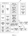
- Fig. 1 is a block diagram illustrating an electronic device 101 in a network environment 100 according to various embodiments.
- the electronic device 101 in the network environment 100 may communicate with an electronic device 102 via a first network 198 (e.g., a short-range wireless communication network), or an electronic device 104 or a server 108 via a second network 199 (e.g., a long-range wireless communication network).
- the electronic device 101 may communicate with the electronic device 104 via the server 108.
- the electronic device 101 includes a processor 120, memory 130, an input device 150, a sound output device 155, a display device 160, an audio module 170, a sensor module 176, an interface 177, a haptic module 179, a camera module 180, a power management module 188, a battery 189, a communication module 190, a subscriber identification module(SIM) 196, or an antenna module 197.
- SIM subscriber identification module
- the electronic device 101 includes a processor 120, memory 130, an input device 150, a sound output device 155, a display device 160, an audio module 170, a sensor module 176, an interface 177, a haptic module 179, a camera module 180, a power management module 188, a battery 189, a communication module 190, a subscriber identification module(SIM) 196, or an antenna module 197.
- one or more other components may be added in the electronic device 101.
- some of the components may be implemented as single integrated circuitry.
- the processor 120 may execute, for example, software (e.g., a program 140) to control at least one other component (e.g., a hardware or software component) of the electronic device 101 coupled with the processor 120, and may perform various data processing or computation. According to one embodiment, as at least part of the data processing or computation, the processor 120 may load a command or data received from another component (e.g., the sensor module 176 or the communication module 190) in volatile memory 132, process the command or the data stored in the volatile memory 132, and store resulting data in non-volatile memory 134.
- software e.g., a program 140
- the processor 120 may load a command or data received from another component (e.g., the sensor module 176 or the communication module 190) in volatile memory 132, process the command or the data stored in the volatile memory 132, and store resulting data in non-volatile memory 134.
- the processor 120 may include a main processor 121 (e.g., a central processing unit (CPU) or an application processor (AP)), and an auxiliary processor 123 (e.g., a graphics processing unit (GPU), an image signal processor (ISP), a sensor hub processor, or a communication processor (CP)) that is operable independently from, or in conjunction with, the main processor 121.
- auxiliary processor 123 may be adapted to consume less power than the main processor 121, or to be specific to a specified function.
- the auxiliary processor 123 may be implemented as separate from, or as part of the main processor 121.
- the auxiliary processor 123 may control at least some of functions or states related to at least one component (e.g., the display device 160, the sensor module 176, or the communication module 190) among the components of the electronic device 101, instead of the main processor 121 while the main processor 121 is in an inactive (e.g., sleep) state, or together with the main processor 121 while the main processor 121 is in an active state (e.g., executing an application).
- the auxiliary processor 123 e.g., an image signal processor or a communication processor
- the memory 130 may store various data used by at least one component (e.g., the processor 120 or the sensor module 176) of the electronic device 101.
- the various data may include, for example, software (e.g., the program 140) and input data or output data for a command related thererto.
- the memory 130 may include the volatile memory 132 or the non-volatile memory 134.
- the program 140 may be stored in the memory 130 as software, and may include, for example, an operating system (OS) 142, middleware 144, or an application 146.
- OS operating system
- middleware middleware
- application application
- the input device 150 may receive a command or data to be used by other component (e.g., the processor 120) of the electronic device 101, from the outside (e.g., a user) of the electronic device 101.
- the input device 150 may include, for example, a microphone, a mouse, a keyboard, or a digital pen (e.g., a stylus pen).
- the sound output device 155 may output sound signals to the outside of the electronic device 101.
- the sound output device 155 may include, for example, a speaker or a receiver.
- the speaker may be used for general purposes, such as playing multimedia or playing record, and the receiver may be used for an incoming calls. According to an embodiment, the receiver may be implemented as separate from, or as part of the speaker.
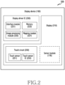
- the display device 160 may visually provide information to the outside (e.g., a user) of the electronic device 101.
- the display device 160 may include, for example, a display, a hologram device, or a projector and control circuitry to control a corresponding one of the display, hologram device, and projector.
- the display device 160 may include touch circuitry adapted to detect a touch, or sensor circuitry (e.g., a pressure sensor) adapted to measure the intensity of force incurred by the touch.
- the antenna 370 may be disposed between the rear housing 330 and the battery 360.
- the antenna 370 may include a near field communication (NFC) antenna, a wireless charging antenna, and/or a magnetic secure transmission (MST) antenna.
- the antenna 370 may perform a near field communication with an external device, or wirelessly transmit or receive power required for charging.
- a part of the support portion 321 and/or the lateral housing 320 may further include an antenna radiator so as to form an antenna structure together with the antenna 370.
- a conductor 323 may be prepared to cover at least a part of the opening 322 of the support portion 321.
- the conductor 323 may shift a parasitic resonance frequency, which may occur at the opening 322, into outband so as to function to prevent the antenna performance degradation.
- the electronic device may receive the ultrasonic wave having been transmitted to and then reflected by the external object.
- the fingerprint sensor 540 may receive the reflected ultrasonic wave and then convert the energy of the reflected ultrasonic wave into localized electric charges. These electric charges may be collected by pixel input electrodes of the fingerprint sensor 504, and be transmitted to pixel circuits. The electric charges may be amplified by the pixel circuits.
- the electronic device may generate a fingerprint image corresponding to the external object, at least based on the received ultrasonic wave.
- the fingerprint sensor 540 may output a digital signal in order to constitute an image (for example, a fingerprint image) of the external object 550.
- the fingerprint sensor 540 may provide the digital signal for the processor.
- the processor may generate a fingerprint image by using the digital signal.
- an application specific integrated circuit (ASIC) for the fingerprint sensor 540 may generate the fingerprint image by using the digital signal.
- the ASIC may provide the generated fingerprint image for the processor.
- an ultrasonic wave may be transmitted through a complex between the fingerprint sensor 540 and the exposed surface 511, as a medium.
- an ultrasonic wave and a reflected ultrasonic wave that the fingerprint sensor 540 generates and receives, respectively may use a complex lamination including the transparent member 510, the display panel 520, and the light absorbing member 530, as a transmitting path.
- a complex lamination including the transparent member 510, the display panel 520, and the light absorbing member 530, as a transmitting path.
- a fingerprint sensor 640 (for example, the fingerprint sensor 540 of FIG. 5A ) may be disposed under a lamination in which a transparent member 610 (for example, the transparent member 510 of FIG. 5A ), a display panel 620 (for example, the display panel 520 of FIG. 5A ), and a light absorbing member 630 (for example, the light absorbing member 530 of FIG. 5A ) are sequentially laminated.
- the light absorbing member 630 may include: a base layer 631 (for example, the base layer 531 of FIG. 5A ); and a first adhesive layer 632 (or an upper adhesive layer, for example, the first adhesive layer 532 of FIG.
- the first adhesive layer 631 may prevent external visibility due to the photoelectric effect of a region to which the fingerprint sensor 640 is attached and minimize the damage to the display panel 620 so as to prevent external visibility of an attachment mark of the fingerprint sensor 640.
- the light absorbing member 630 may include an opening for receiving the fingerprint sensor 640.
- the second adhesive layer 633 of the light absorbing member 630 may include an opening 633a.
- An area of the opening 633a may be larger than an area of the fingerprint sensor 640 so as to enable the fingerprint sensor 640 to be attached thereto.
- the opening 633a may have an area corresponding to a fingerprint detection region S1 (for example, 311 of FIG. 4 ) of the transparent member 610.
- the base layer 631 may be exposed to the outside in a region 631a in which the opening 633a is formed.
- the light absorbing member 630 may be manufactured according to a method in which, in a process of disposing the first adhesive layer 632 and the second adhesive layer 633 on the opposite surfaces of the base layer 631, the adhesive layers are disposed only in a region excluding the opening 633a.
- the opening 633a may be formed by a process of disposing the first adhesive layer 632 and/or the second adhesive layer 633 on the base layer 631 after the masking treatment on the region 631a exposed to the outside.
- An adhesive agent 650 may be used to bond the fingerprint sensor 640 to the exposed region 631a through the opening 633a.
- the liquid adhesive agent 650 may be applied to the exposed region 631a and an inner surface of the opening 633a.
- the fingerprint sensor 640 may be attached to the base layer 631 by means of the applied adhesive agent 650.
- the liquid adhesive agent 650 may be hardened and solidified after the fingerprint sensor 640 is positioned in a designated region. That is, the fingerprint sensor 640 may be fixedly attached to the base layer 631 by means of a liquid bonding method.
- a process of removing bubbles in the liquid adhesive agent 650 may be added.
- the electronic device 101 may include an additional base 634 and an additional adhesive layer 635.
- the fingerprint sensor 640 may be disposed under a lamination in which the transparent member 610, the display panel 620, and the light absorbing member 630 are sequentially laminated.
- the first adhesive layer 632, the base layer 631, and the second adhesive layer 633 may be sequentially disposed under the display panel 620.
- the light absorbing member 630 may further include a second base layer 634 and a third adhesive layer 635 between the second adhesive layer 633 and the base layer 631.
- the light absorbing member 630 may include an opening 630a for receiving the fingerprint sensor 640.
- the second adhesive layer 633, the second base layer 634, and the third adhesive layer 635 of the light absorbing member 630 may include openings 633a, 634a, and 635a.
- the opening 630a may be formed to have a size capable of receiving the fingerprint sensor 640 so as to enable the fingerprint sensor 640 to be mounted therein.
- the opening 630a may be formed to correspond to the fingerprint detection region of the transparent member 610.
- the first base layer 631 may be exposed to the outside due to the formation of the opening 633a.
- the light absorbing member 630 may be formed by a process of laminating the third adhesive layer 635, the second base layer 634, and the second adhesive layer 633 on the first base layer 631 after the masking treatment on the region 631a, which is exposed to the outside, of the first base layer 631, and then removing the masking.
- the third adhesive layer 635, the second base layer 634, and the second adhesive layer 633 which include the openings 633a, 634a, and 635a formed therethrough to correspond to the exposed region 631a of the first base layer 631, may be laminated on the first base layer 631.
- a display panel may secure sufficient adhesive force and a waterproof effect by means of the first adhesive layer 633 and the third adhesive layer 635.
- the fingerprint sensor 640 may have an improved detection performance.
- the first adhesive layer 633 and the third adhesive layer 635 may be formed to have suitable thicknesses.
- the transparent member 610 and the display panel 620 may be curved.
- the third adhesive layer 635 may be formed to have a suitable thickness.
- the first adhesive layer 633 may be formed to have a suitable thickness in order to secure a performance of a fingerprint sensor.
- the light absorbing member 630 may be formed to be different in each of a region corresponding to the ultrasonic sensor 640 and a remaining region, the light absorbing member 630 may be formed to be suitable for a function of each of the regions.
- the adhesive agent 650 may be used to bond the fingerprint sensor 640 to the exposed region 631a through the openings 633a, 634a, and 635a.
- the liquid adhesive agent 650 may be applied to the exposed region 631a and an inner surface of the opening 633a.
- the fingerprint sensor 640 may be attached to the base layer 631 by means of the applied adhesive agent 650.
- the liquid adhesive agent 650 may be hardened and solidified after the fingerprint sensor 640 is positioned in a designated region. That is, the fingerprint sensor 640 may be fixedly attached to the base layer 631 by means of a liquid bonding method. In an embodiment, a process of removing bubbles in the liquid adhesive agent 650 may be added.
- FIG. 6D is a cross-sectional view of a state where the fingerprint sensor 640 according to embodiments of the disclosure may be attached under the transparent member 610, the display panel 620, and the light absorbing member 630.
- the acoustic impedance may be mathematically proportional to the density and sound velocity of a medium.
- the sound velocity may be proportional to a square root of the bulk modulus of the medium, and the bulk modulus of a solid may indicate the Young's modulus (or the elastic modulus). That is, elastic moduli of media may be a major factor in the impedance matching.
- the base layer 631 of the light absorbing member 630 may be made of a polymer material.
- the elastic modulus of the polymer material may be approximately 2 to 3 GPa.
- the first adhesive layer 632 and the second adhesive layer 633 may be made of an acrylic material, and the elastic modulus of the acrylic material may be approximately 0.1 MPa, and it is thus noted that the transmission rate of ultrasonic waves may be lowered due to the impedance mismatching between media made of the polymer material and the acrylic material. Therefore, the fingerprint sensor 640 according to an embodiment of the disclosure may be fixedly attached to the base layer 631 while being in close contact with the same, by using the adhesive agent 650, not the second adhesive layer 633.
- the adhesive agent 650 may be made of an epoxy material.
- the elastic modulus of the epoxy material may be approximately 2 GPa. That is, the impedance matching is possible between the adhesive agent 650 made of the epoxy material and the base layer 631 made of the polymer material. Therefore, the fingerprint sensor 640 according to one embodiment may be fixedly attached to the base layer 631 by means of the separate adhesive agent 650, not the second adhesive layer 633, and thus have an improved fingerprint recognition performance.
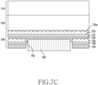
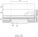
- FIGS. 7A to 7D are cross-sectional views illustrating examples of a light absorbing member of an electronic device according to embodiments of the disclosure.
- a transparent member 710 for example, the transparent member 610 of FIGS. 6A to 6D
- a display panel 720 for example, the display panel 620 of FIGS. 6A to 6D
- a fingerprint sensor 740 the fingerprint sensor 640 of FIGS. 6A to 6D
- an adhesive agent 750 for example, the adhesive agent 650 of FIGS. 6A to 6D
- FIGS. 7A to 7D may be at least partially equal or similar to the components described in FIGS. 6A to 6D , and overlapping descriptions thereof are omitted.
- embodiments described in FIGS. 7A to 7D are described in the embodiments of FIGS. 6A to 6D , but it is natural that the addition of a configuration not shown in FIGS. 7A to 7D is not limited.
- the light absorbing member 730 may include a base layer 731, a black coated layer 732, a first adhesive layer 733, and a second adhesive layer 734.
- the black coated layer 732 may be disposed on the base layer 731.
- the black coated layer 732 may be disposed under the base layer 731.
- the black coated layer 732 may be disposed on the base layer 731.
- the black coated layer 732 may absorb at least a part of external light incident into the fingerprint sensor 740 through the transparent member 710 and the display panel 720.
- the black coated layer 732 enables an inner part (for example, the fingerprint sensor 740) of an electronic device to be invisible through the transparent member 710 and the display panel 720 which becomes transparent when the display panel does not operate.
- the first adhesive layer 733 of the light absorbing member 730 may include an embossed pattern 733a formed on the first adhesive layer 733 in order to minimize or remove bubbles which may be formed on an adhesion surface with the display panel 720.
- the first base layer 732 may be made of a polymer material (for example, PET) in order to maintain a shape of the first adhesive layer 733.
- the embossed pattern 733a may include a dot pattern, a stripe pattern, a grid pattern, and the like.
- the first adhesive layer 733 including the embossed pattern 733a may be referred to as a formed adhesive layer, and the entire of the light absorbing member 730 may be referred to as an embossed layer.
- the first adhesive layer 733 of the light absorbing member 730 may include a flat portion 733b at a position corresponding to a fingerprint detection region S2 (for example, 311 of FIG. 4 ).
- the flat portion 733b may be formed at a position corresponding to the fingerprint sensor 740.
- the flat portion 733b may be formed on a transmitting path of at least one ultrasonic wave generated and received by the fingerprint sensor 740, the transmitting path being between the fingerprint sensor 740 and an exposed surface 711 of the transparent member 710.
- An adhesion surface between the first adhesive layer 733 and the display panel 720 may contain air due to at least one space 733c formed between protrusions of the embossed pattern 733c.
- An ultrasonic wave may have the great energy loss when a phase of a medium is changed (for example, a phase change from a solid to a gas).
- the acoustic impedance of air has a very small value of approximately 0.004 p/uS.
- the air contained in the space 733c of the first adhesive layer 733 may incur the serious acoustic impedance mismatching.
- the flat portion 733b enables the first adhesive layer 733 to be attached to the display panel 720 while being in close contact with the same, so as to prevent the formation of bubbles between the first adhesive layer 733 and the display panel 720 in the fingerprint detection region S2.
- the flat portion 733b may function to enable an ultrasonic wave to be transmitted without the great energy dissipation between the fingerprint sensor 740 and the transparent member 710. Therefore, the flat portion 733b may contribute to the performance improvement in the fingerprint recognition function of the fingerprint sensor 740.
- the light absorbing member 730 may include the first adhesive layer 733, the first base layer 731, the black coated layer 732, and the second adhesive layer 734, and may further include a third adhesive layer 735 and a second base layer 736 between the second adhesive layer 734 and the black coated layer 732.
- the third adhesive layer 735 may include an embossed pattern formed on the third adhesive layer 735 in order to minimize or remove bubbles which may be formed on an adhesion surface with the first base layer 731.
- the third adhesive layer 735 including the embossed pattern may be attached to the first base layer 731 while being in close contact with the same, and may thus improve a waterproof performance of a lateral side of the display panel 720 and increase the adhesive force.
- the first base layer 731 and the second base layer 736 may be made of a polymer material (for example, PET) in order to maintain embossed shapes of the first adhesive layer 733 and the third adhesive layer 735.
- a polymer material for example, PET
- the first, second, and third adhesive layers 733, 734, and 735 may be configured to have various thicknesses.
- the first adhesive layer 733 may be manufactured to have a thin thickness for a performance of the fingerprint sensor 740
- the third adhesive layer 735 may be manufactured to have a thick thickness in order to secure a waterproof performance of an electronic device and the adhesive force of the display panel 720.
- the first, second, and third adhesive layers 733, 734, and 735 may be formed to have suitable thicknesses in light of the adhesive force, a waterproof performance, and a performance of the fingerprint sensor 740.
- the fingerprint detection region S2 may include the flat portion 733b and a remaining region may include the embossed pattern 733c.
- the flat portion 733b may be formed on an ultrasonic wave transmitting path between the ultrasonic fingerprint sensor 740 and the exposed surface 711 of the transparent member 710.
- An adhesion surface between the first adhesive layer 733 and the display panel 720 may contain air due to at least one space 733c formed between protrusions of the embossed pattern 733c.
- the flat portion 733b enables the first adhesive layer 733 to be attached to the display panel 720 while being in close contact with the same, so as to prevent the formation of bubbles between the first adhesive layer 733 and the display panel 720 in the fingerprint detection region S2.
- the flat portion 733b may function to enable an ultrasonic wave to be transmitted without the great energy dissipation between the fingerprint sensor 740 and the transparent member 710. Therefore, the flat portion 733b may contribute to the performance improvement in the fingerprint recognition function of the fingerprint sensor 740.
- the transparent member 710 and the display panel 720 may have edge shapes whose edge has the curvature.
- a thickness of the third adhesive layer 735 in each of edge regions of the transparent member 710 and the display panel 720 may be suitably formed to secure a waterproof performance in order to protect the display panel 720.
- an embossed pattern 733d in the fingerprint detection region S2 may be different from the embossed pattern 733a of a remaining region.
- a width of the embossed pattern 733d disposed in the fingerprint detection region S2 may be formed to be wide, and a width of an embossed pattern groove 733e may be formed to be narrow.
- the width of the embossed pattern 733d in the fingerprint detection region S2 may be formed to be wide, and the adhesive layer 733 in the fingerprint detection region S2 may thus contain less bubbles.
- a height of the groove 733e and a width of the groove 733e may be formed to be small, and a space containing air may be thus formed to be small and contain less bubbles.
- the embossed pattern 733d and the groove 733e of the first adhesive layer 733 in the fingerprint detection region S2 may be variously formed to minimize bubbles contained in the first adhesive layer 733 in the fingerprint detection region S2.
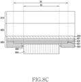
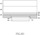
- FIGS. 8A to 8D are cross-sectional views illustrating other examples of a light absorbing member of an electronic device according to embodiments of the disclosure.
- a transparent member 810 for example, the transparent member 710 of FIGS. 7A to 7E
- a display panel 820 for example, the display panel 720 of FIGS. 7A to 7E
- a fingerprint sensor 840 for example, the fingerprint sensor 740 of FIGS. 7A to 7E
- an adhesive agent 850 for example, the adhesive agent 750 of FIGS. 7A to 7E
- FIGS. 8A and 8D may be at least partially equal or similar to the components described in FIGS. 6A to 7B , and overlapping descriptions thereof are omitted.
- embodiments described in FIGS. 8A and 8D are described in the embodiments of FIGS. 6A to 7B , but it is natural that the addition of a configuration not shown in FIGS. 8A and 8B is not limited.
- a light absorbing member 830 may include a base layer 831, a black coated layer 832, a noise shielding layer 833, a first adhesive layer 834, and a second adhesive layer 835.
- the noise shielding layer 833 may shield noise which may occur at the display panel 820 and the like, and thus improve the electro-magnetic compatibility (EMC) of the fingerprint sensor 840.
- the noise shielding layer 833 may be disposed on the black coated layer 832.
- the noise shielding layer 833 may be formed according to a film transfer method, printing, or a printing method. For example, as illustrated, the noise shielding layer 833 may be disposed under the black coated layer 832.
- the noise shielding layer 833 may be disposed on the base layer 831. In another embodiment, the noise shielding layer 833 may be interposed between the base layer 831 and the black coated layer 832. Embodiments are not limited thereto, and with reference to the base layer 831, the black coated layer 832 and the noise shielding layer 833 may have various laminating orders or arrangement relations therebetween.
- a light absorbing member 830 may include: a base layer 831; a conductive black coated layer 836 disposed on the base layer 831; and a first adhesive layer 834 and a second adhesive layer 835 which are disposed on one surface of the base layer 831 and one surface of the conductive black coated layer 836, respectively.
- the conductive black coated layer 836 may be made of a conductive ink.
- the conductive black coated layer 836 enables internal parts (for example, 101 of FIG. 4 ) of an electronic device including the fingerprint sensor 840 to be invisible, and may also have a shielding function.
- a light absorbing member 830 may include a base layer 831, a black coated layer 832, a noise shielding member 837, a first adhesive layer 834, and a second adhesive layer 835.
- the noise shielding member 837 may shield noise which may occur at a display panel 820 and the like, and thus improve the electro-magnetic compatibility (EMC) of the fingerprint sensor 840.
- the noise shielding member 837 may be attached on the black coated layer 832.
- the noise shielding member 837 may be attached under the black coated layer 832. In a view from above, the noise shielding member 837 may be attached to a position corresponding to the fingerprint sensor 840.
- the noise shielding member 837 may be disposed on the black coated layer 832 at a position corresponding to a fingerprint detection region S3 (for example, 311 of FIG. 4 ).
- the noise shielding member 837 may have an area correspond to the fingerprint detection region S3 of a transparent member 810 or may have an area S4 larger than the same.
- the noise shielding member 837 may have the area S4 capable of completely covering the fingerprint sensor 840 and thus improve the electro-magnetic compatibility.
- a fingerprint sensor 840 may include a noise shielding portion 841.
- the noise shielding portion 841 may be disposed at the outermost side in which the fingerprint sensor 840 faces a display panel 820.
- the fingerprint sensor 840 including the noise shielding portion 841 may be attached to a lamination of a transparent member 810, the display panel 820, and a light absorbing member 830.
- the noise shielding portion 841 may be fixedly attached to a black coated layer 832 disposed on a base layer 831 by using an adhesive agent 850.
- Embodiments are not limited thereto, and the fingerprint sensor 840 including the noise shielding portion 841 may be attached to a lamination in accordance with any suitable method.
- An embodiment, in which the fingerprint sensor 840 includes a noise shielding member will be concretely described in FIGS. 10 and 12E to 12J.
- FIGS. 9A and 9B are cross-sectional views illustrating other examples of an arrangement structure of a fingerprint sensor in an electronic device according to embodiments of the disclosure.
- a transparent member 910 for example, the transparent member 810 of FIGS. 8A to 8D
- a display panel 920 for example, the display panel 820 of FIGS. 8A to 8D
- a light absorbing member 930 for example, the light absorbing member 830 of FIGS. 8A to 8D
- a fingerprint sensor 940 for example, the fingerprint sensor 840 of FIGS. 8A to 8D
- an adhesive agent 950 for example, the adhesive agent 850 of FIGS. 8A to 8D
- FIGS. 9A to 9B may be at least partially equal or similar to the components described in FIGS. 6A to 8D , and overlapping descriptions thereof are omitted.
- embodiments described in FIGS. 9A and 9B are described in the embodiments of FIGS. 6A to 8D , but may further include a configuration not illustrated in FIGS. 9A and 9B .
- an electronic device may include a buffer member 960 (or a cushion layer) attached to a lamination of a transparent member 910, a display panel 920, and a light absorbing member 930.
- the buffer member 960 may be attached to the light absorbing member 930 by means of the adhesive force of a second adhesive layer 934.
- the buffer member 960 may be made of an elastic material which is compressed while being pressed and is recovered to an original shape while being released.
- the buffer member 960 may include multiple air holes to prepare for compression which is caused when the buffer member is pressed.
- the air holes included in the buffer member 960 may cause the energy loss due to the acoustic impedance mismatching between the air (gas) contained in the air holes and the buffer member (solid), and diffused reflection of ultrasonic waves due to an irregular shape or arrangement of the air holes. That is, it may not be desirable to position the buffer member 960 on an ultrasonic wave transmitting path.
- the buffer member 960 may not be disposed between a fingerprint sensor 940 (or a detector (for example, an ultrasonic wave oscillator and/or an ultrasonic wave receiver) of the fingerprint sensor 940) and a fingerprint detection region (for example, 311 of FIG. 3A ).
- the buffer member 960 may include an opening 961 for receiving the fingerprint sensor 940.
- the opening 961 of the buffer member 960 may have an area at least partially corresponding to the second adhesive layer 934 of the light absorbing member 930.
- the buffer member 960 may be designed to have a lowest surface b2 which is lower than or level with a lowest surface (or a baseline) b1 of the fingerprint sensor 940.
- the fingerprint sensor 940 may not protrude to the outside beyond the buffer member 960.
- the buffer member 960 may be formed to be higher than the fingerprint sensor 940. Accordingly, the buffer member 960 may prevent the fingerprint sensor 940 from being damaged due to not only the external impact applied to the transparent member 910 but also the impact which may be caused below.
- an electronic device may include a buffer member 960 and a heat-radiating plate 970, which are attached to a lamination of a transparent member 910, a display panel 920, and a light absorbing member 930.
- the heat-radiating plate 970 may be attached under the buffer member 960.
- An adhesive layer 971 may be interposed between the heat-radiating plate 970 and the buffer member 960 to enable the same to be attached to each other.
- the heat-radiating plate 970 may block heat generated from other electronic parts included in the electronic device.
- a main processor, a graphic processing unit, a communication processor, and a battery for example, 360 of FIG.
- the heat-radiating plate 970 may block heat transmission from these electronic parts and thus prevent the degradation in performances of the display panel 920 and the fingerprint sensor 940.
- the heat-radiating plate 970 may be designed to cover at least a part of the fingerprint sensor 940.
- the heat-radiating plate 970 may include a slit 972 through which a flexible printed circuit board (FPCB) 941 is withdrawn, and the FPCB transfers power and/or a signal of the fingerprint sensor 940 to at least one processor.
- the slit 972 may have a length which is equal to or longer than a width of the FPCB 941.
- FIG. 10 is a cross-sectional view illustrating an example of a structure of a fingerprint sensor in an electronic device according to embodiments of the disclosure.
- a transparent member 1010 for example, the transparent member 910 of FIGS. 9A and 9B
- a display panel 1020 for example, the display panel 920 of FIGS. 9A and 9B
- a light absorbing member 1030 for example, the light absorbing member 930 of FIGS. 9A and 9B
- an adhesive agent for example, the adhesive agent 950 of FIGS. 9A and 9B
- FIG. 10 may be at least partially equal or similar to the components described in FIGS. 6A to 9B , and overlapping descriptions thereof are omitted.
- an embodiment described in FIG. 10 is described in the embodiments of FIGS. 6A to 9B , but may further include a configuration not illustrated in FIG. 10 .
- a fingerprint sensor 1040 may further include an impact preventing portion.
- the fingerprint sensor 1040 may include a detector 1042 disposed on a printed circuit board 1041, a noise shielding layer 1043 for shielding noise affecting the detector 1042, and a conductive member 1044 for connecting the noise shielding layer 1043 to an earthing portion of the printed circuit board 1041.
- the detector 1042 may include an ultrasonic wave receiver and/or an ultrasonic wave oscillator.
- the buffer member 1050 may be disposed between the detector 1042 and the conductive member 1044.
- the buffer member 1050 may include: an impact preventing member 1051 including multiple air holes for compression and recovery; a first adhesive layer 1052a; and a second adhesive layer 1052b.
- the first adhesive layer 1052a and the second adhesive layer 1052b may attach the impact preventing member 1051 to the noise shielding layer 1043 and the printed circuit board 1041, respectively.
- the fingerprint sensor 1040 includes the buffer member 1050
- the fingerprint sensor 1040 and the detector 1042 may be prevented from being damaged due to not only the external impact at the top (for example, the transparent member 1010) but also the impact which may be caused below.
- the buffer member 1050 may have a height higher than a height of the detector 1042, and the impact caused below may be thus prevented from being directly applied to the detector 1042.
- the first adhesive layer 1052a and the second adhesive layer 1052b may be used as adhesive members for fixing the conductive member 1044 between the noise shielding layer 1043 and the earthing portion of the printed circuit board 1041.
- the first adhesive layer 1052a and the second adhesive layer 1052b may include a conductive tape so as to be electrically connected to the noise shielding layer 1043.
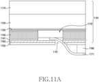
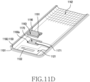
- FIGS. 11A to 11D illustrate other examples of an arrangement structure of a fingerprint sensor in an electronic device according to embodiments of the disclosure.
- a transparent member 1110 for example, the transparent member 1010 of FIG. 10
- a display panel 1120 for example, the display panel 1020 of FIG. 10
- a fingerprint sensor 1170 for example, the fingerprint sensor 1040 of FIG. 10
- an adhesive agent 1150 which are illustrated in FIGS. 11A to 11D , may be at least partially equal or similar to the components described in FIGS. 6A to 10 , and overlapping descriptions thereof are omitted.
- embodiments described in FIGS. 11A to 11D are described in the embodiments of FIGS. 6A to 10 , but may further include a configuration not illustrated in FIGS. 11A to 11D .
- an electronic device may further include a detecting panel 1160 (for example, a digitizer panel) attached to a lamination 1101 of a transparent member 1110, a display panel 1120, a light absorbing member 1130, and a buffer member 1140.
- the detecting panel 1160 may further include a heat-radiating plate 1150.
- the detecting panel 1160 may be attached under the buffer member 1140.
- An adhesive layer 1141 may be interposed between the detecting panel 1160 and the buffer member 1140 so as to enable the same to be attached to each other.
- the heat-radiating plate 1150 may be disposed under the detecting panel 1160. In another embodiment, the heat-radiating plate 1150 may be disposed on the detecting panel 1160.
- the detecting panel 1160 and/or the heat-radiating plate 1150 may be disposed to substantially cover the entire region of the transparent member 1110.
- the detecting panel 1160 may have an area corresponding to an activated region of the display panel 1120. Therefore, in a view from above, the detecting panel 1160 may be designed to cover at least a part of a fingerprint sensor 1170.
- the detecting panel 1160 may include a slit 1161 through which a first flexible printed circuit board 1171 for connecting the fingerprint sensor 1170 to a main printed circuit board is withdrawn.
- the slit 1161 may have a length which is equal to or longer than a width of the first flexible printed circuit board 1171.
- the fingerprint sensor 1170 may be operatively connected to at least one processor (for example, the processor 120 of FIG. 1 ) in order to receive a driving signal or transmit detected fingerprint information.
- an operational connection between a fingerprint sensor and at least one processor may be achieved through a printed circuit board.
- An interconnection method between printed circuit boards may be applied as one method among a method (for example, a connector) using a coupling method, a bonding method (for example, soldering) using heat, light, or the like, a contact method (for example, a pogo-pin and a C-clip), a connection method (for example, and a conductive adhesive agent) using an adhesive agent, or a combination thereof.
- the first flexible printed circuit board 1171 of the fingerprint sensor 1170 may be connected to a second flexible printed circuit board 1121 connected to the main printed circuit board 1180 so as to transmit, to at least one processor, power and a signal for controlling the display panel 1120.
- the second flexible printed circuit board 1121 may include at least one processor 1122 (for example, a driver IC) mounted thereon and operating the display panel 1120.
- a printed circuit board for the fingerprint sensor 1170 and a printed circuit board for the display panel 1120 may be integrally formed.
- an integrated printed circuit board of the fingerprint sensor 1170 and the display panel 1120 may be directly connected to a main printed circuit board.
- the integrated printed circuit board may be connected to the main printed circuit board through a sub printed circuit board.
- a detecting panel 1160 may include an opening 1160a in which a fingerprint sensor 1170 may be mounted. An area of the opening 1160a may be larger than an area of the fingerprint sensor 1170 so as to enable the fingerprint sensor 1170 to be mounted therein.
- the detecting panel 1160 may further include an auxiliary detecting panel 1190.
- the auxiliary detecting panel 1190 may have an area capable of covering the opening 1160a, and may be disposed at a position at which the auxiliary detecting panel may cover the opening 1160a.
- the auxiliary detecting panel 1190 may include an auxiliary conductive pattern 1163.
- a plurality of conductive patterns 1161 formed on the detecting panel 1160 and the auxiliary conductive pattern 1163 of the auxiliary detecting panel 1190 may be electrically connected to each other.
- the electrical connection between the plurality of conductive patterns 1161 and the auxiliary conductive pattern 1163 may employ at least one of soldering, wiring, a pogo-pin, and a C-clip.
- the plurality of conductive patterns 1161 and the auxiliary detecting panel 1190 may be electrically connected to each other through solder 1164.
- the detecting panel 1160 may detect an indication position by using the auxiliary conductive pattern 1163 included in the auxiliary detecting panel 1190, even in a region in which the opening 1160a is formed.
- the auxiliary detecting panel 1190 may include a slit 1191 through which a first flexible printed circuit board 1171 for connecting the fingerprint sensor 1170 to at least one processor, is withdrawn.
- the slit 1191 may be formed to be at least one of an opening formed through one lateral surface of the auxiliary detecting panel 1190 and a long hole formed through the auxiliary detecting panel.
- Embodiments are not limited thereto, and even in an embodiment including the auxiliary detecting panel 1190, a slit for the first flexible printed circuit board 1171 may be formed on the detecting panel 1160.
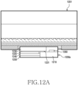
- FIGS. 12A to 12F illustrate examples of a structure of a fingerprint sensor according to an embodiment of the disclosure.
- Fingerprint sensors described in FIGS. 12A to 12F may be embodiments of the fingerprint sensors 640, 740, 840, 940, 1040, and 1170 described in FIGS. 6A to 11D .
- a fingerprint sensor 1200a may be attached to a lamination 1201 including a transparent member, a display panel, and a light absorbing member.
- the lamination 1201 may be one of the various embodiments described in FIGS. 6A to 11D , in which the fingerprint sensor is attached, or have a combination structure of at least two or more embodiments.
- the fingerprint sensor 1200a may include a base substrate 1210, and an ultrasonic wave oscillator 1220, an ultrasonic wave receiver 1230, a first oscillator electrode 1240, and a sound absorbing member 1250 which are mounted on the base substrate.
- the ultrasonic wave oscillator 1220 may generate an ultrasonic wave by using the piezoelectric effect.
- a second oscillator electrode 1231 may be interposed between the ultrasonic wave receiver 1230 and the ultrasonic wave oscillator 1220.
- the ultrasonic wave oscillator 1220 may generate an ultrasonic wave by repeating expansion and contraction by means of a voltage applied by the first oscillator electrode 1240 and the second oscillator electrode 1231 which are disposed on upper and lower surfaces thereof.
- the first oscillator electrode 1240 and the second oscillator electrode 1231 may be metal layers with which the upper and lower surfaces of the ultrasonic wave oscillator 1220 are coated.
- the ultrasonic wave receiver 1230 may include a piezoelectric reception layer and an array of pixel circuits arranged on a substrate (or a backplane).
- each of pixel circuits may include a circuit wire and at least one thin film transistor film element.
- the ultrasonic wave receiver 1230 may include a piezoelectric reception layer and an array of pixel circuits arranged on a substrate made of glass.
- the ultrasonic wave receiver 1230 may receive an ultrasonic wave reflected from an external object (for example, 550 of FIG. 5A ), and convert the energy of the received ultrasonic wave into electric charges through a piezoelectric reception layer.
- the fingerprint sensor 1200a may be configured to provide an image of the external object by using these electric charges.
- the ultrasonic wave receiver 1230 and the ultrasonic wave oscillator 1220 are overlappingly and vertically laminated, and the fingerprint sensor 1200a according to one embodiment may be thus alternately operated according to divided operations including an ultrasonic wave generation operation of the ultrasonic wave oscillator 1220 and an ultrasonic wave reception operation of the ultrasonic wave receiver 1230.
- an ultrasonic wave generated by the ultrasonic wave oscillator 1220 may be not only transmitted to an exposed surface (for example, 711 of FIG. 7A ) of a transparent member through the ultrasonic wave receiver 1230, but also generated toward an inner part of an electronic device (for example, 101 of FIG. 4 ), namely in a direction opposite to the exposed surface.
- the sound absorbing member 1250 may function to absorb the ultrasonic wave generated toward the opposite direction.
- the sound absorbing member 1250 may be made of any suitable elastic material.
- the sound absorbing member 1250 may be made of a porous material so as to absorb an ultrasonic wave.
- the porous material may be a material containing many micro holes or gaps therein.
- a sound wave incident into the porous material may be transmitted through air in a hole or a gap so as to be penetrated into the material.
- the penetrated sound wave may be converted into the thermal energy inside the sound absorbing member 1250, and thus prevent the performance degradation due to an ultrasonic wave of other electronic parts or the fingerprint sensor 1200a in advance.
- the sound absorbing member 1250 may include an epoxy film.
- the ultrasonic wave receiver 1230 of the fingerprint sensor 1200a may include a polymer material.
- the ultrasonic wave receiver 1230 may include a thin film transistor film layer, a piezoelectric reception layer, and an array of a plurality of pixel circuits arranged on a substrate (or a backplane) made of a polymer material.
- components with which the ultrasonic wave receiver 1230 may mate may indicate an acrylic adhesive layer (for example, 533 of FIG. 5A ), an epoxy-based adhesive agent (for example, 650 of FIG. 6D ), a polymer-based base layer (for example, 631 of FIG. 6D ), and the like.
- the elastic modulus of glass may be approximately 65-69 GPa.
- the elastic moduli of the epoxy-based material, PET based on a polymer, and the acrylic material may be approximately 2 GPa, 2.7 GPa, and 0.1 MPa, respectively.
- the elastic modulus of glass may be greatly different from the elastic moduli of general materials which function as a medium of an ultrasonic wave in an electronic device according to an embodiment of the disclosure. Therefore, by comparing with a case in which the ultrasonic wave receiver 1230 is formed to be a substrate made of glass, when the ultrasonic wave receiver is formed to be a substrate made of a polymer material, the impedance matching may be easily achieved, and the transmission rate of an ultrasonic wave may be improved. Accordingly, the fingerprint sensor 1200a may have an improved fingerprint recognition function.
- the fingerprint sensor 1200a including the ultrasonic wave receiver 1230 made of a polymer material can be attached, by means of a roll forming process, to a lamination including at least one of a transparent member, a display panel, and a light absorbing member.
- a process of bonding the fingerprint sensor 1200a, by means of the roll forming, to a module which includes a display panel and is prepared as a single module including an impact preventing layer (for example, 960 of FIGS. 9A and 9B ), a detecting panel (for example, 1160 of FIG. 11A ), and the like is possible.
- the fingerprint sensor or a display panel may be damaged due to the glass broken by the pressure of a roller in the roll forming process, while in the case of the ultrasonic wave receiver 1230 made of a polymer material, the roll forming process is possible, and a process of mounting the fingerprint sensor 1200a may be thus easily performed.
- the fingerprint sensor 1200a may include a processor 1260 (or a controller) of a fingerprint sensor, the processor applying a driving signal to a detector (for example, the ultrasonic wave oscillator 1220 and the ultrasonic wave receiver 1230).
- the processor 1260 may be mounted on the base substrate 1210 of the fingerprint sensor 1200a.
- the processor 1260 may be referred to as an ultrasonic fingerprint sensor controller or an application specific integrated circuit (ASIC).
- the processor 1260 and the detectors 1220 and 1230 may be implemented together as a module such as a chip size package (CSP) or a wafer level package (WLP).
- CSP chip size package
- WLP wafer level package
- Embodiments are not limited thereto, and the processor 1260 of the fingerprint sensor may be disposed on a main printed circuit board (for example, 350 of FIG. 4 ) or a printed circuit board (for example, 1121 of FIG. 11A ) of a display panel.
- a main printed circuit board for example, 350 of FIG. 4
- a printed circuit board for example, 1121 of FIG. 11A
- a sound absorbing member 1250 may be separately implemented from a fingerprint sensor 1200b.
- the sound absorbing member 1250 may be disposed to be spaced a predetermined distance (g) apart from an ultrasonic wave oscillator 1240.
- An ultrasonic wave (of the opposite direction) generated by the ultrasonic wave oscillator 1240 may be transmitted to the sound absorbing member 1250 spaced the predetermined distance (g) apart therefrom by using air as a medium.
- the sound absorbing member 1250 may thus effectively absorb the remaining ultrasonic waves.
- the sound absorbing member 1250 disposed separately from the fingerprint sensor 1200b may be attached to various components positioned under the fingerprint sensor 1200b.
- the sound absorbing member 1250 may be fixed to one of a main printed circuit board (for example, 350 of FIG. 4 ), a battery (for example, 360 of FIG. 4 ), and a rear housing (for example, 320 of FIG. 4 ), which may be positioned under the fingerprint sensor 1200b.
- a fingerprint sensor 1200c may include a noise shielding layer 1280.
- the noise shielding layer 1280 may shield noise which may occur at the display panel 820 and the like and thus improve the electro-magnetic compatibility (EMC) of the fingerprint sensor 1280.
- the noise shielding layer 1280 may cover a detector (for example, the ultrasonic wave receiver 1230) of the fingerprint sensor 1200e.
- the noise shielding layer 1280 may be electrically connected to an earthing portion 1211 (or an earthing pad) of a base substrate 1210 so as to be earthed.
- a conductive adhesive layer 1281 (or a conductive tape) may be interposed between the noise shielding layer 1280 and the earthing portion 1211.
- the noise shielding layer 1280 may be electrically connected to the earthing portion 1211 by using at least one method among soldering, wiring, a pogo-pin, and a C-clip.
- a fingerprint sensor 1200d may has a structure in which an ultrasonic wave oscillator 1220 and an ultrasonic wave receiver 1230 are horizontally arranged.
- the ultrasonic wave oscillator 1220 and the ultrasonic wave receiver 1230 which are arranged according to the horizontal arrangement structure, do not mutually overlap each other, and are thus simultaneously operable, thereby improving the fingerprint recognition speed.
- a noise shielding layer 1280 may have a size and a shape which are capable of covering both the ultrasonic wave oscillator 1220 and the ultrasonic wave receiver 1230.
- the noise shielding layer 1280 may have a size and a shape which are capable of covering only the ultrasonic wave receiver 1230.
- an ultrasonic wave oscillator 1220 and/or an ultrasonic wave receiver 1230 which are horizontally arranged according to an embodiment, may be disposed to be inclined.
- the ultrasonic wave oscillator 1220 may be disposed to be inclined at a predetermined angle ( ⁇ ) with reference to the horizontal.
- the reception rate of an ultrasonic wave which is reflected from an external object (for example, 550 of FIG. 5A ) and then received by the ultrasonic wave receiver 1230 may be increased in comparison to an ultrasonic wave generated by the ultrasonic wave oscillator 1220.
- a fingerprint sensor 1200e may have an improved fingerprint recognition rate.
- Embodiments are not limited thereto, and the ultrasonic wave receiver 1230 may be disposed to be inclined and both the ultrasonic wave oscillator 1220 and the ultrasonic wave receiver 1230 may be disposed to be inclined toward each other.
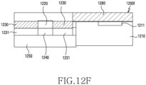
- FIG. 12F illustrates various arrangement examples of the ultrasonic wave oscillator 1220 and the ultrasonic wave receiver 1230.
- the ultrasonic wave receiver 1230 may be disposed to enclose at least a part of the ultrasonic wave oscillator 1220.
- a fingerprint sensor 1200f may have an improved fingerprint recognition rate.
- the fingerprint sensor 1220f, in which the ultrasonic wave receiver 1230 according to one embodiment is disposed to enclose at least a part of the ultrasonic wave oscillator 1220 may further include a noise shielding layer 1280.
- the noise shielding layer 1280 may be disposed to cover at least a part of a detector (the ultrasonic wave receiver 1230 and the ultrasonic wave oscillator 1220).
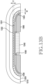
- FIGS. 13A and 13B are cross-sectional views illustrating other examples of a light absorbing member according to a display panel structure in an electronic device according to an embodiment of the disclosure.
- a fingerprint sensor 1340 (for example, the fingerprint sensor 540 of FIG. 5A ) may be disposed under a lamination in which a transparent member 1310 (for example, the transparent member 1110 of FIG. 11A ), a display panel 1320 (for example, the display panel 1120 of FIG. 11A ), and a light absorbing member 1330 (for example, the light absorbing member 1130 of FIG. 11A ) are sequentially laminated. At least one edge of the transparent member 1310 may have the curvature.
- the display panel 1320 may be laminated under the transparent member 1310, and may be formed to correspond to a shape of a lower surface of the transparent member 1310. As shown in FIGS.
- the transparent member 1310 and the display panel 1320 may be configured in a two-side edge structure in which opposite edges have the curvature. According to various embodiments, the transparent member 1310 and the display panel 1320 may be configured in a four-side edge structure in which all edges have the curvature.
- the light absorbing member 1330 may include: a base layer 1331; and a first adhesive layer 1332 (or an upper adhesive layer) and a second adhesive layer 1333 (or a lower adhesive layer) which are disposed on opposite surfaces of the base layer 1331.
- a thickness t1 of the first adhesive layer 1332 corresponding to a flat region of the transparent member 1310 and a thickness t2 of the first adhesive layer 1332 corresponding to an edge region of the transparent member 1310 may be formed to be different.
- a thickness of the first adhesive layer 1332 in a flat region P1 may be properly selected in order to improve a performance of the fingerprint sensor 1340.
- the first adhesive layer 1332 in the flat region P1 may be formed to have the minimum thickness in order to secure a performance of the fingerprint sensor 1340.
- the thickness t2 of the first adhesive layer 1332 in an edge region P2 may be thicker than the thickness t1 of the first adhesive layer 1332 in the flat region P1. In the edge region P2, the adhesive force of the display panel 1320 is reduced, and a waterproof problem may thus occur. According to various embodiments, in order to improve the adhesive force and/or the waterproof performance of the edge region P2 of the display panel 1320, the first adhesive layer 1332 in the edge region P2 may be formed to be thick. The thickness of the first adhesive layer 1332 in each of the flat region P1 and the edge region P2 may be properly configured to secure the adhesive force and/or the waterproof performance of a display module as well as a performance of the fingerprint sensor 1340.
- the light absorbing member 1330 may further include an additional adhesive layer (for example, the third adhesive layer 635 of FIG. 6B ) and an additional base layer (for example, the second base layer 634 of FIG. 6B ) between the base layer 1331 and the second adhesive layer 1333.
- an additional adhesive layer for example, the third adhesive layer 635 of FIG. 6B
- an additional base layer for example, the second base layer 634 of FIG. 6B
- the base layer 1331 may be formed to be bent at a boundary portion between the flat region P1 and the edge region P2 in order to obtain a shape of the first adhesive layer 1332. Through the bent portion, the thickness of the first adhesive layer 1332 may be formed to be different in each of the flat region P1 and the edge region P2.
- the light absorbing member 1330 may include an opening formed therethrough to receive the fingerprint sensor 1340.
- the second adhesive layer 1333 may include an opening formed to be larger than the fingerprint sensor 1340 to enable the fingerprint sensor 1340 to be received therein.
- an opening 1333a may have an area corresponding to a fingerprint detection region S1 (for example, 311 of FIG. 4 ) of the transparent member 1310.
- the base layer 1331 may be exposed to the outside in a region 1331a including the opening 1333a formed therein.
- the light absorbing member 1330 may be manufactured according to a method in which, in a process of disposing the first adhesive layer 1332 and the second adhesive layer 1333 on the opposite surfaces of the base layer 1331, the adhesive layers are disposed only in a region excluding the opening 1333a.
- the additional base layer and the additional adhesive layer may also include openings formed therethrough to correspond to the second adhesive layer 1333.
- a thickness of the second adhesive layer 1333 may be configured to be different in each of the flat region P1 and the edge region P2.
- the illustrated second adhesive layer 1333 is formed to have a thin thickness in the edge region P2, and may thus correspond to a shape of a buffer member 1360.
- the thickness of the second adhesive layer 1333 may be formed to be uniform, and the second adhesive layer 1333 may be formed to correspond to a shape of the base layer 1331.
- the fingerprint sensor 1340 may be attached to the base layer 1331 by using an adhesive agent 1350.
- the liquid adhesive agent 1350 may be applied to the exposed region 1331a and an inner surface of the opening 1333a. After the liquid adhesive agent 1350 is applied, a process of removing bubbles existing between the liquid adhesive agent 1350 and the base layer 1331 may be added.
- the buffer member 1360 (for example, the buffer member 960 of FIG. 9A ) may be attached under the second adhesive layer 1333. As described above, an elastic material may be applied to the buffer member 1360 in order to absorb and mitigate external impact applied to the transparent member 1310. In addition, the buffer member 1360 may be disposed not to be positioned on an ultrasonic wave transmitting path.
- the fingerprint sensor 1340 may be disposed not to protrude to the outside beyond the buffer member 1360.
- the buffer member 1360 may prevent the fingerprint sensor 1340 from being damaged due to not only the external impact applied to the transparent member 1310 but also the impact which may be caused below.
- the buffer member 1360 may extend, from a lateral side of an opening 1360a, to cover at least a part of an exposed surface of the fingerprint sensor 1340.
- an adhesion surface, which faces a display panel 1320, of a first adhesive layer 1332 may have an embossed pattern.
- the first adhesive layer 1332 including the embossed pattern may be attached to the display panel 1320 while being in close contact with the same, and may thus improve a waterproof performance of a lateral side of the display panel 1320 and increase the adhesive force.
- the first adhesive layer 1332 may be formed to have various thicknesses.
- a thickness t2 of the first adhesive layer 1332 in an edge region may be formed to be thicker than a thickness t1 of the first adhesive layer 1332 in a flat region. In the edge region, the first adhesive layer 1332 may have a thick thickness and thus secure the improved adhesive force and waterproof performance.
- the first adhesive layer 1332 in the flat region may be formed to be flat instead of having the embossed pattern.
- the electronic device may further include a heat-radiating plate (not shown), a detecting panel (a digitizer panel, not shown), a pressure sensor, and the like, which are not illustrated in FIGS. 13A and 13B . That is, the electronic device may further include a configuration which is described in FIGS. 6A to 12F , but not illustrated in FIGS. 13A and 13B .
- An electronic device may include: a transparent member (for example, the transparent member 610 of FIG. 6B ); a display panel disposed under the transparent member (for example, the display panel 620 of FIG. 6B ); an ultrasonic sensor (for example, the ultrasonic sensor 640 of FIG. 6B ) disposed under the display panel and acquiring biometric information from an external object adjacent to the transparent member by using an ultrasonic wave having been transmitted through the display panel and the transparent member; and a light absorbing member (for example, the light absorbing member 630 of FIG. 6B ) for absorbing at least a part of external light incident into the ultrasonic sensor through the transparent member and the display panel, wherein the light absorbing member is disposed between the display panel and the ultrasonic sensor.
- a transparent member for example, the transparent member 610 of FIG. 6B
- a display panel disposed under the transparent member (for example, the display panel 620 of FIG. 6B );
- an ultrasonic sensor for example, the ultrasonic sensor 640 of FIG
- the light absorbing member may be formed to have a different thickness for each of a region corresponding to the ultrasonic sensor and a remaining region.
- the light absorbing member may include: a first base layer (for example, the first base layer 631 of FIG. 6B ); a first adhesive layer (for example, the first adhesive layer 632 of FIG. 6B ) disposed on the first base layer to be attached to the display panel; and a second adhesive layer (for example, the second adhesive layer 635 of FIG. 6B ) disposed under the first base layer.
- a first base layer for example, the first base layer 631 of FIG. 6B
- a first adhesive layer for example, the first adhesive layer 632 of FIG. 6B
- a second adhesive layer for example, the second adhesive layer 635 of FIG. 6B
- the first adhesive layer may include at least one embossed pattern (for example, the embossed pattern 733a of FIG. 7C ) formed on a surface facing the display panel.
- the first adhesive layer may include a flat portion formed on a surface thereof facing the display panel, in at least a part of a region corresponding to the ultrasonic sensor.
- the second adhesive layer may include an opening (for example, the opening 630a of FIG. 6B ) formed in a region corresponding to the ultrasonic sensor.
- the ultrasonic sensor may be attached to one part of the first base layer, the one part being exposed through the opening, by means of an adhesive agent (for example, the adhesive agent 650 of FIG. 6B ) disposed between the ultrasonic sensor and the one part of the first base layer.
- an adhesive agent for example, the adhesive agent 650 of FIG. 6B
- the light absorbing member may further include: a third adhesive layer (for example, the third adhesive layer 635 of FIG. 6B ) disposed between the second adhesive layer and the first base layer; and a second base layer (for example, the second base layer 634 of FIG. 6B ) disposed under the third adhesive layer.
- a third adhesive layer for example, the third adhesive layer 635 of FIG. 6B
- a second base layer for example, the second base layer 634 of FIG. 6B
- the second adhesive layer, the second base layer, and the third adhesive layer may include openings (for example, the opening 630a of FIG. 6B ) formed in a region corresponding to the ultrasonic sensor.
- An electronic device may further include a conductive member (for example, the conductive member 1044 of FIG. 10 ) for blocking noise occurring at the display panel, and the conductive member may be electrically connected to an earthing portion of the electronic device, between the light absorbing member and the ultrasonic sensor.
- a conductive member for example, the conductive member 1044 of FIG. 10
- the conductive member may be electrically connected to an earthing portion of the electronic device, between the light absorbing member and the ultrasonic sensor.
- the conductive member may be connected to an earthing portion of the electronic device through the connection with an earthing pad (for example, the earthing portion 1211 (or the earthing pad) of FIG. 12C ) on a printed circuit board of the ultrasonic sensor, and the ultrasonic sensor may further include a conductive tape (for example, the conductive adhesive layer 1280 (or the conductive tape) of FIG. 12C ) so as to electrically connect the conductive member and the earthing pad.
- an earthing pad for example, the earthing portion 1211 (or the earthing pad) of FIG. 12C
- the ultrasonic sensor may further include a conductive tape (for example, the conductive adhesive layer 1280 (or the conductive tape) of FIG. 12C ) so as to electrically connect the conductive member and the earthing pad.
- the light absorbing member may include a black coated layer and a conductive member for blocking noise occurring at the display panel, which are disposed between the first adhesive layer and the second adhesive layer.
- the conductive member may at least cover a region corresponding to the ultrasonic sensor.
- An electronic device may further include a buffer member (for example, the buffer member 960 of FIG. 9A ) for mitigating the impact toward a direction in which the display panel is pressed, the buffer member being disposed under at least a part of the light absorbing member positioned on a lateral side of the ultrasonic sensor, and the buffer member may be formed to be higher than a height of the ultrasonic sensor.
- a buffer member for example, the buffer member 960 of FIG. 9A
- the buffer member being disposed under at least a part of the light absorbing member positioned on a lateral side of the ultrasonic sensor, and the buffer member may be formed to be higher than a height of the ultrasonic sensor.
- An electronic device may further include a detecting panel (for example, the detecting panel 1160 of FIG. 11A ) disposed under at least a part of the buffer member.
- a detecting panel for example, the detecting panel 1160 of FIG. 11A
- the detecting panel may include a slit (for example, the slit 1161 of FIG. 11A ) through which a printed circuit board of the ultrasonic sensor is withdrawn.
- the ultrasonic sensor may include an ultrasonic wave oscillator (for example, the ultrasonic wave oscillator 1220 of FIG. 12A ) for oscillating an ultrasonic wave, and an ultrasonic wave receiver (for example, the ultrasonic wave receiver 1230 of FIG. 12B ) for receiving the ultrasonic wave reflected from an external object, wherein at least a part of the ultrasonic wave receiver may be disposed while being in close contact with the light absorbing member.
- an ultrasonic wave oscillator for example, the ultrasonic wave oscillator 1220 of FIG. 12A
- an ultrasonic wave receiver for example, the ultrasonic wave receiver 1230 of FIG. 12B
- An electronic device may include: a transparent member (for example, the transparent member 1310 of FIG. 13A ) including a planar region (for example, the planar region P1 of FIG. 13A ) and a curved region (for example, the curved region P2 of FIG. 13A ) disposed on at least one edge of the planar region; a display panel (for example, the display panel 1320 of FIG. 13A ) disposed under the transparent member and including a planar region and a curved region formed to correspond to a shape of the transparent member; an ultrasonic sensor (for example, the ultrasonic sensor 1340 of FIG.
- an light absorbing member for example, the light absorbing member 1330 of FIG. 13A ) for absorbing at least a part of external light incident into the ultrasonic sensor through the transparent member and the display panel, wherein the light absorbing member is disposed between the display panel and the ultrasonic sensor, and the light absorbing member positioned under the planar region may be formed to have a different thickness from the light absorbing member positioned under the curved region.
- the light absorbing member may include: a first base layer (for example, the first base layer 1310 of FIG. 13A ); a first adhesive layer (for example, the first adhesive layer 1332 of FIG. 13A ) disposed on the first base layer to be attached to the display panel; and a second adhesive layer (for example, the second adhesive layer 1333 of FIG. 13A ) disposed under the first base layer.
- a first base layer for example, the first base layer 1310 of FIG. 13A
- a first adhesive layer for example, the first adhesive layer 1332 of FIG. 13A
- second adhesive layer for example, the second adhesive layer 1333 of FIG. 13A
- a thickness (for example, t2 of FIG. 13A ) of the first adhesive layer in a region corresponding to the curved region may be formed to be thicker than a thickness (for example, t1 of FIG. 13A ) of the first adhesive layer in a region corresponding to the planar region.
- the first adhesive layer may fill a space between the curved region of the display panel and a curved region of the first base layer.
Landscapes
- Engineering & Computer Science (AREA)
- Theoretical Computer Science (AREA)
- Physics & Mathematics (AREA)
- General Engineering & Computer Science (AREA)
- General Physics & Mathematics (AREA)
- Human Computer Interaction (AREA)
- Computer Hardware Design (AREA)
- Signal Processing (AREA)
- Computer Security & Cryptography (AREA)
- Multimedia (AREA)
- Software Systems (AREA)
- Devices For Indicating Variable Information By Combining Individual Elements (AREA)
- Electromagnetism (AREA)
- Power Engineering (AREA)
- Acoustics & Sound (AREA)
- User Interface Of Digital Computer (AREA)
Claims (16)
- Elektronische Vorrichtung (101), umfassend:ein transparentes Element (510, 610, 710, 810, 910, 1010, 1110, 1310);eine Anzeigetafel (410, 520, 620, 720, 820, 920, 1020, 1120, 1320), die unter dem transparenten Element angeordnet ist; undeinen Ultraschallsensor (430, 540, 640, 740, 840, 940, 1040, 1170, 1200a-f, 1300b, 1340), der unter der Anzeigetafel angeordnet und konfiguriert ist, um biometrische Informationen von einem externen Objekt zu erfassen, das auf dem transparenten Element berührt wird, indem eine Ultraschallwelle verwendet wird, die durch die Anzeigetafel und das transparente Element übertragen wurde;dadurch gekennzeichnet, dass die elektronische Vorrichtung ferner ein lichtabsorbierendes Element (420, 530, 630, 730, 830, 930, 1030, 1130, 1330) umfasst, das zwischen der Anzeigetafel und dem Ultraschallsensor angeordnet und so konfiguriert ist, dass es mindestens einen Teil von durch das transparente Element und die Anzeigetafel in den Ultraschallsensor einfallendem externem Lichts absorbiert,wobei der Ultraschallsensor einen Ultraschallwellenempfänger (1230) zum Empfangen der von dem externen Objekt reflektierten Ultraschallwelle enthält und mindestens ein Teil des Ultraschallwellenempfängers in engem Kontakt mit dem lichtabsorbierenden Element angeordnet ist.
- Elektronische Vorrichtung nach Anspruch 1, wobei der Ultraschallsensor ferner einen Ultraschallwellenoszillator (1220) zum In-Schwingungen-Versetzen der Ultraschallwelle enthält, und
der Ultraschallwellenempfänger und der Ultraschallwellenoszillator vertikal geschichtet sind. - Elektronische Vorrichtung nach Anspruch 2, wobei eine Ultraschallwellenschwingung durch den Ultraschallwellenoszillator und ein Ultraschallwellenempfang durch den Ultraschallwellenempfänger abwechselnd arbeiten.
- Elektronische Vorrichtung nach Anspruch 2, ferner umfassend ein schallabsorbierendes Element (1250), das so konfiguriert ist, dass es eine Ultraschallwelle absorbiert, die vom Ultraschallwellenoszillator in einer dem Ultraschallwellenempfänger entgegengesetzten Richtung in Schwingung versetzt wird,
wobei das schallabsorbierende Element in einem vorbestimmten Abstand vom Ultraschallwellenoszillator beabstandet ist. - Elektronische Vorrichtung nach Anspruch 1, wobei der Ultraschallwellenempfänger ein Polymermaterial enthält.
- Elektronische Vorrichtung nach Anspruch 1, wobei das transparente Element einen ebenen Bereich und einen gekrümmten Bereich enthält, der an mindestens einer Kante des ebenen Bereichs angeordnet ist,die Anzeigetafel einen ebenen Bereich und einen gekrümmten Bereich enthält, der so ausgebildet ist, dass er einer Form des transparenten Elements entspricht, unddas lichtabsorbierende Element so ausgebildet ist, dass es für jeden eines Bereichs, der dem ebenen Bereich entspricht, und eines Bereichs, der dem gekrümmten Bereich entspricht, eine unterschiedliche Dicke aufweist.
- Elektronische Vorrichtung nach Anspruch 6, wobei das lichtabsorbierende Element eine erste Basisschicht, eine erste Klebeschicht, die auf der ersten Basisschicht angeordnet ist, um an der Anzeigetafel befestigt zu werden, und eine zweite Klebeschicht, die unter der ersten Basisschicht angeordnet ist, enthält.
- Elektronische Vorrichtung nach Anspruch 7, wobei die erste Klebeschicht mindestens ein Prägemuster auf einer der Anzeigetafel zugewandten Oberfläche davon enthält.
- Elektronische Vorrichtung nach Anspruch 8, wobei die erste Klebeschicht einen flachen Abschnitt enthält, der auf einer der Anzeigetafel zugewandten Oberfläche davon in mindestens einem Teil eines Bereichs, der dem Ultraschallsensor entspricht, ausgebildet ist.
- Elektronische Vorrichtung nach Anspruch 7, wobei die zweite Klebeschicht eine Öffnung enthält, die in einem Bereich ausgebildet ist, der dem Ultraschallsensor entspricht, und
der mindestens eine Teil des Ultraschallwellenempfängers mittels eines Klebemittels, das zwischen dem mindestens einen Teil des Ultraschallwellenempfängers und dem einen Teil der ersten Basisschicht angeordnet ist, in engem Kontakt mit einem Teil der ersten Basisschicht angeordnet ist, wobei der eine Teil durch die Öffnung freiliegt. - Elektronische Vorrichtung nach Anspruch 7, wobei das lichtabsorbierende Element ferner eine dritte Klebeschicht, die zwischen der zweiten Klebeschicht und der ersten Basisschicht angeordnet ist, und eine zweite Basisschicht, die unter der dritten Klebeschicht angeordnet ist, enthält, und
die zweite Klebeschicht, die zweite Basisschicht und die dritte Klebeschicht Öffnungen enthalten, die in einem Bereich ausgebildet sind, der dem Ultraschallsensor entspricht. - Elektronische Vorrichtung nach Anspruch 7, wobei das lichtabsorbierende Element eine schwarz beschichtete Schicht (732, 832, 836) und eine Abschirmungsschicht (833) enthält, die so konfiguriert sind, dass sie an der Anzeigetafel auftretende Geräusche blockieren, und die zwischen der ersten Klebeschicht und der zweiten Klebeschicht angeordnet sind.
- Elektronische Vorrichtung nach Anspruch 1, ferner umfassend ein Pufferelement (960, 1050, 1140, 1360), das unter mindestens einem Teil des lichtabsorbierenden Elements angeordnet ist, das auf einer lateralen Seite des Ultraschallsensors positioniert und so konfiguriert ist, dass es Stöße in eine Richtung abschwächt, in der die Anzeigetafel gedrückt wird,
wobei das Pufferelement so ausgebildet ist, dass es höher ist als die Höhe des Ultraschallsensors. - Elektronische Vorrichtung nach Anspruch 7, wobei eine Dicke der ersten Klebeschicht in einem Bereich, der dem gekrümmten Bereich entspricht, dicker ausgebildet ist als eine Dicke der ersten Klebeschicht in einem Bereich, der dem ebenen Bereich entspricht.
- Elektronische Vorrichtung nach Anspruch 7, wobei die erste Klebeschicht einen Raum zwischen dem gekrümmten Bereich der Anzeigetafel und einem gekrümmten Bereich der ersten Basisschicht füllt.
- Elektronische Vorrichtung nach Anspruch 7, wobei der zumindest eine Teil des Ultraschallwellenempfängers in engem Kontakt mit dem lichtabsorbierenden Element basierend auf der zweiten Klebeschicht angeordnet ist.
Applications Claiming Priority (4)
| Application Number | Priority Date | Filing Date | Title |
|---|---|---|---|
| KR20170160146 | 2017-11-28 | ||
| KR1020180090973A KR102623203B1 (ko) | 2017-11-28 | 2018-08-03 | 디스플레이 패널과 초음파 센서 사이에 광흡수 부재가 배치된 전자 장치 |
| PCT/KR2018/014759 WO2019107890A1 (ko) | 2017-11-28 | 2018-11-28 | 디스플레이 패널과 초음파 센서 사이에 광흡수 부재가 배치된 전자 장치 |
| EP18883518.5A EP3716008B1 (de) | 2017-11-28 | 2018-11-28 | Elektronische vorrichtung mit einem zwischen einer anzeigetafel und einem ultraschallsensor angeordneten, lichtabsorbierenden element |
Related Parent Applications (1)
| Application Number | Title | Priority Date | Filing Date |
|---|---|---|---|
| EP18883518.5A Division EP3716008B1 (de) | 2017-11-28 | 2018-11-28 | Elektronische vorrichtung mit einem zwischen einer anzeigetafel und einem ultraschallsensor angeordneten, lichtabsorbierenden element |
Publications (4)
| Publication Number | Publication Date |
|---|---|
| EP4235467A2 EP4235467A2 (de) | 2023-08-30 |
| EP4235467A3 EP4235467A3 (de) | 2023-10-25 |
| EP4235467B1 true EP4235467B1 (de) | 2025-02-26 |
| EP4235467C0 EP4235467C0 (de) | 2025-02-26 |
Family
ID=66844926
Family Applications (2)
| Application Number | Title | Priority Date | Filing Date |
|---|---|---|---|
| EP18883518.5A Active EP3716008B1 (de) | 2017-11-28 | 2018-11-28 | Elektronische vorrichtung mit einem zwischen einer anzeigetafel und einem ultraschallsensor angeordneten, lichtabsorbierenden element |
| EP23177546.1A Active EP4235467B1 (de) | 2017-11-28 | 2018-11-28 | Elektronische vorrichtung mit einem zwischen einer anzeigetafel und einem ultraschallsensor angeordneten, lichtabsorbierenden element |
Family Applications Before (1)
| Application Number | Title | Priority Date | Filing Date |
|---|---|---|---|
| EP18883518.5A Active EP3716008B1 (de) | 2017-11-28 | 2018-11-28 | Elektronische vorrichtung mit einem zwischen einer anzeigetafel und einem ultraschallsensor angeordneten, lichtabsorbierenden element |
Country Status (5)
| Country | Link |
|---|---|
| US (1) | US11126293B2 (de) |
| EP (2) | EP3716008B1 (de) |
| KR (1) | KR102623203B1 (de) |
| CN (1) | CN111433708B (de) |
| AU (1) | AU2018377602B2 (de) |
Families Citing this family (14)
| Publication number | Priority date | Publication date | Assignee | Title |
|---|---|---|---|---|
| KR20200014601A (ko) * | 2018-08-01 | 2020-02-11 | 삼성전자주식회사 | 안테나 어레이를 포함하는 전자 장치 |
| KR102704800B1 (ko) | 2019-02-19 | 2024-09-09 | 삼성전자주식회사 | 센서를 포함하는 디스플레이 모듈의 제조 방법 및 디스플레이 모듈을 포함하는 전자 장치 |
| CN112150916B (zh) * | 2019-06-27 | 2022-05-20 | Oppo广东移动通信有限公司 | 曲面显示屏及其驱动方法和电子设备 |
| KR20210029017A (ko) | 2019-09-05 | 2021-03-15 | 삼성전자주식회사 | 광 센서 모듈을 포함하는 전자 장치 |
| KR102905733B1 (ko) | 2019-10-21 | 2025-12-31 | 삼성디스플레이 주식회사 | 생체 감지 기능을 갖는 표시 장치 및 그것의 동작 방법 |
| KR102927726B1 (ko) | 2020-02-21 | 2026-02-13 | 삼성디스플레이 주식회사 | 폴더블 표시 장치 |
| CN112183396B (zh) * | 2020-09-30 | 2024-03-08 | 京东方科技集团股份有限公司 | 显示组件和显示装置 |
| KR20220075008A (ko) * | 2020-11-26 | 2022-06-07 | 삼성디스플레이 주식회사 | 표시 장치 및 표시 장치의 제조 방법 |
| CN112633166B (zh) * | 2020-12-23 | 2022-12-09 | 厦门天马微电子有限公司 | 一种超声波指纹识别模组、显示模组和电子设备 |
| EP4338137B1 (de) * | 2021-07-23 | 2026-01-28 | Google LLC | Zeitsteuerung eines fingerabdrucksensors unter einer anzeige |
| KR20230045718A (ko) | 2021-09-28 | 2023-04-05 | 삼성디스플레이 주식회사 | 표시 장치 |
| CN114115454B (zh) * | 2021-10-21 | 2024-07-23 | 维沃移动通信有限公司 | 电子设备及控制方法 |
| KR20230132646A (ko) | 2022-03-08 | 2023-09-18 | 삼성디스플레이 주식회사 | 전자장치의 제조방법 |
| TWI909142B (zh) * | 2023-03-14 | 2025-12-21 | 緯創資通股份有限公司 | 儀表板裝置、移動載具及移動載具的身份驗證方法 |
Family Cites Families (15)
| Publication number | Priority date | Publication date | Assignee | Title |
|---|---|---|---|---|
| US9323393B2 (en) | 2013-06-03 | 2016-04-26 | Qualcomm Incorporated | Display with peripherally configured ultrasonic biometric sensor |
| US9551783B2 (en) * | 2013-06-03 | 2017-01-24 | Qualcomm Incorporated | Display with backside ultrasonic sensor array |
| US9790126B2 (en) * | 2013-09-05 | 2017-10-17 | Apple Inc. | Opaque color stack for electronic device |
| KR101700998B1 (ko) | 2014-01-02 | 2017-01-31 | 삼성전기주식회사 | 지문 감지 센서 및 이를 포함하는 전자 기기 |
| US9224030B2 (en) | 2014-01-10 | 2015-12-29 | Qualcomm Incorporated | Sensor identification |
| JP2016029475A (ja) * | 2014-07-22 | 2016-03-03 | 株式会社ジャパンディスプレイ | 液晶表示装置及び電子機器 |
| US10139479B2 (en) | 2014-10-15 | 2018-11-27 | Qualcomm Incorporated | Superpixel array of piezoelectric ultrasonic transducers for 2-D beamforming |
| KR101769740B1 (ko) | 2015-01-23 | 2017-08-21 | 크루셜텍 (주) | 지문센서 패키지 및 이의 제조방법 |
| KR102097179B1 (ko) | 2015-04-07 | 2020-04-03 | 앰코테크놀로지코리아(주) | 지문센서 패키지 및 그 제조 방법 |
| US9710689B2 (en) | 2015-10-30 | 2017-07-18 | Essential Products, Inc. | Fingerprint sensors for mobile devices |
| US10229316B2 (en) * | 2016-01-29 | 2019-03-12 | Synaptics Incorporated | Compound collimating system using apertures and collimators |
| KR20170104314A (ko) | 2016-03-07 | 2017-09-15 | 주식회사 아모센스 | 지문 감지 센서 |
| KR102534273B1 (ko) * | 2016-03-25 | 2023-05-19 | 삼성디스플레이 주식회사 | 플렉서블 표시장치 |
| KR101796660B1 (ko) | 2016-04-19 | 2017-11-10 | 삼성전자주식회사 | 지문 인식 기능을 지원하는 전자 장치 및 이의 운용 방법 |
| EP3236390B1 (de) * | 2016-04-19 | 2021-11-24 | Samsung Electronics Co., Ltd. | Elektronische vorrichtung zur unterstützung der verifizierung von fingerabdrücken und verfahren zum betrieb davon |
-
2018
- 2018-08-03 KR KR1020180090973A patent/KR102623203B1/ko active Active
- 2018-11-28 US US16/767,915 patent/US11126293B2/en active Active
- 2018-11-28 EP EP18883518.5A patent/EP3716008B1/de active Active
- 2018-11-28 CN CN201880077924.8A patent/CN111433708B/zh active Active
- 2018-11-28 AU AU2018377602A patent/AU2018377602B2/en active Active
- 2018-11-28 EP EP23177546.1A patent/EP4235467B1/de active Active
Also Published As
| Publication number | Publication date |
|---|---|
| EP3716008C0 (de) | 2023-06-07 |
| KR102623203B1 (ko) | 2024-01-11 |
| AU2018377602B2 (en) | 2023-09-07 |
| US11126293B2 (en) | 2021-09-21 |
| AU2018377602A1 (en) | 2020-07-16 |
| CN111433708A (zh) | 2020-07-17 |
| EP4235467A3 (de) | 2023-10-25 |
| EP4235467C0 (de) | 2025-02-26 |
| EP3716008B1 (de) | 2023-06-07 |
| EP3716008A4 (de) | 2021-01-27 |
| CN111433708B (zh) | 2023-11-28 |
| US20210004117A1 (en) | 2021-01-07 |
| EP3716008A1 (de) | 2020-09-30 |
| EP4235467A2 (de) | 2023-08-30 |
| KR20190062143A (ko) | 2019-06-05 |
Similar Documents
| Publication | Publication Date | Title |
|---|---|---|
| EP3716008B1 (de) | Elektronische vorrichtung mit einem zwischen einer anzeigetafel und einem ultraschallsensor angeordneten, lichtabsorbierenden element | |
| CN113412462B (zh) | 包括保护构件的可折叠电子装置 | |
| US12080094B2 (en) | Electronic device including biometric sensor | |
| US11281880B2 (en) | Display and electronic device including the same | |
| US20190172875A1 (en) | Electronic device including light blocking member with micro-hole | |
| CN108008778B (zh) | 支持指纹验证的电子装置及其操作方法 | |
| US10939570B2 (en) | Display and electronic device including waterproof structure | |
| US11663847B2 (en) | Electronic device including sensor placed under display | |
| WO2019107890A1 (ko) | 디스플레이 패널과 초음파 센서 사이에 광흡수 부재가 배치된 전자 장치 | |
| CN111309096A (zh) | 包括设置有导电图案的指纹识别模块的电子装置 | |
| RU2775152C1 (ru) | Складное электронное устройство, включающее в себя защитный элемент | |
| EP4350881A1 (de) | Antennenstruktur und elektronische vorrichtung mit der antennenstruktur |
Legal Events
| Date | Code | Title | Description |
|---|---|---|---|
| PUAI | Public reference made under article 153(3) epc to a published international application that has entered the european phase |
Free format text: ORIGINAL CODE: 0009012 |
|
| STAA | Information on the status of an ep patent application or granted ep patent |
Free format text: STATUS: THE APPLICATION HAS BEEN PUBLISHED |
|
| AC | Divisional application: reference to earlier application |
Ref document number: 3716008 Country of ref document: EP Kind code of ref document: P |
|
| AK | Designated contracting states |
Kind code of ref document: A2 Designated state(s): AL AT BE BG CH CY CZ DE DK EE ES FI FR GB GR HR HU IE IS IT LI LT LU LV MC MK MT NL NO PL PT RO RS SE SI SK SM TR |
|
| REG | Reference to a national code |
Ref country code: DE Ref legal event code: R079 Free format text: PREVIOUS MAIN CLASS: G06F0021320000 Ipc: G06F0001160000 Ref document number: 602018079748 Country of ref document: DE |
|
| PUAL | Search report despatched |
Free format text: ORIGINAL CODE: 0009013 |
|
| AK | Designated contracting states |
Kind code of ref document: A3 Designated state(s): AL AT BE BG CH CY CZ DE DK EE ES FI FR GB GR HR HU IE IS IT LI LT LU LV MC MK MT NL NO PL PT RO RS SE SI SK SM TR |
|
| RIC1 | Information provided on ipc code assigned before grant |
Ipc: G06F 1/20 20060101ALN20230915BHEP Ipc: G06F 21/32 20130101ALI20230915BHEP Ipc: G06V 40/13 20220101ALI20230915BHEP Ipc: H04M 1/02 20060101ALI20230915BHEP Ipc: G06F 1/16 20060101AFI20230915BHEP |
|
| STAA | Information on the status of an ep patent application or granted ep patent |
Free format text: STATUS: REQUEST FOR EXAMINATION WAS MADE |
|
| 17P | Request for examination filed |
Effective date: 20240119 |
|
| RBV | Designated contracting states (corrected) |
Designated state(s): AL AT BE BG CH CY CZ DE DK EE ES FI FR GB GR HR HU IE IS IT LI LT LU LV MC MK MT NL NO PL PT RO RS SE SI SK SM TR |
|
| GRAP | Despatch of communication of intention to grant a patent |
Free format text: ORIGINAL CODE: EPIDOSNIGR1 |
|
| STAA | Information on the status of an ep patent application or granted ep patent |
Free format text: STATUS: GRANT OF PATENT IS INTENDED |
|
| RIC1 | Information provided on ipc code assigned before grant |
Ipc: G06F 1/20 20060101ALN20240924BHEP Ipc: G06F 21/32 20130101ALI20240924BHEP Ipc: G06V 40/13 20220101ALI20240924BHEP Ipc: H04M 1/02 20060101ALI20240924BHEP Ipc: G06F 1/16 20060101AFI20240924BHEP |
|
| INTG | Intention to grant announced |
Effective date: 20241004 |
|
| RIN1 | Information on inventor provided before grant (corrected) |
Inventor name: CHOI, HYUNSUK Inventor name: WOO, SUNGGWAN Inventor name: KOO, HYOJUN Inventor name: JO, JEONGGYU Inventor name: RHEE, BONGJAE Inventor name: KIM, JOOHAN Inventor name: KIM, JINMAN |
|
| GRAS | Grant fee paid |
Free format text: ORIGINAL CODE: EPIDOSNIGR3 |
|
| GRAA | (expected) grant |
Free format text: ORIGINAL CODE: 0009210 |
|
| STAA | Information on the status of an ep patent application or granted ep patent |
Free format text: STATUS: THE PATENT HAS BEEN GRANTED |
|
| AC | Divisional application: reference to earlier application |
Ref document number: 3716008 Country of ref document: EP Kind code of ref document: P |
|
| AK | Designated contracting states |
Kind code of ref document: B1 Designated state(s): AL AT BE BG CH CY CZ DE DK EE ES FI FR GB GR HR HU IE IS IT LI LT LU LV MC MK MT NL NO PL PT RO RS SE SI SK SM TR |
|
| REG | Reference to a national code |
Ref country code: GB Ref legal event code: FG4D |
|
| REG | Reference to a national code |
Ref country code: CH Ref legal event code: EP |
|
| REG | Reference to a national code |
Ref country code: DE Ref legal event code: R096 Ref document number: 602018079748 Country of ref document: DE |
|
| REG | Reference to a national code |
Ref country code: IE Ref legal event code: FG4D |
|
| U01 | Request for unitary effect filed |
Effective date: 20250319 |
|
| U07 | Unitary effect registered |
Designated state(s): AT BE BG DE DK EE FI FR IT LT LU LV MT NL PT RO SE SI Effective date: 20250324 |
|
| PG25 | Lapsed in a contracting state [announced via postgrant information from national office to epo] |
Ref country code: RS Free format text: LAPSE BECAUSE OF FAILURE TO SUBMIT A TRANSLATION OF THE DESCRIPTION OR TO PAY THE FEE WITHIN THE PRESCRIBED TIME-LIMIT Effective date: 20250526 |
|
| PG25 | Lapsed in a contracting state [announced via postgrant information from national office to epo] |
Ref country code: PL Free format text: LAPSE BECAUSE OF FAILURE TO SUBMIT A TRANSLATION OF THE DESCRIPTION OR TO PAY THE FEE WITHIN THE PRESCRIBED TIME-LIMIT Effective date: 20250226 |
|
| PG25 | Lapsed in a contracting state [announced via postgrant information from national office to epo] |
Ref country code: ES Free format text: LAPSE BECAUSE OF FAILURE TO SUBMIT A TRANSLATION OF THE DESCRIPTION OR TO PAY THE FEE WITHIN THE PRESCRIBED TIME-LIMIT Effective date: 20250226 |
|
| PG25 | Lapsed in a contracting state [announced via postgrant information from national office to epo] |
Ref country code: NO Free format text: LAPSE BECAUSE OF FAILURE TO SUBMIT A TRANSLATION OF THE DESCRIPTION OR TO PAY THE FEE WITHIN THE PRESCRIBED TIME-LIMIT Effective date: 20250526 Ref country code: IS Free format text: LAPSE BECAUSE OF FAILURE TO SUBMIT A TRANSLATION OF THE DESCRIPTION OR TO PAY THE FEE WITHIN THE PRESCRIBED TIME-LIMIT Effective date: 20250626 |
|
| PG25 | Lapsed in a contracting state [announced via postgrant information from national office to epo] |
Ref country code: HR Free format text: LAPSE BECAUSE OF FAILURE TO SUBMIT A TRANSLATION OF THE DESCRIPTION OR TO PAY THE FEE WITHIN THE PRESCRIBED TIME-LIMIT Effective date: 20250226 |
|
| PG25 | Lapsed in a contracting state [announced via postgrant information from national office to epo] |
Ref country code: GR Free format text: LAPSE BECAUSE OF FAILURE TO SUBMIT A TRANSLATION OF THE DESCRIPTION OR TO PAY THE FEE WITHIN THE PRESCRIBED TIME-LIMIT Effective date: 20250527 |
|
| PG25 | Lapsed in a contracting state [announced via postgrant information from national office to epo] |
Ref country code: SM Free format text: LAPSE BECAUSE OF FAILURE TO SUBMIT A TRANSLATION OF THE DESCRIPTION OR TO PAY THE FEE WITHIN THE PRESCRIBED TIME-LIMIT Effective date: 20250226 |
|
| PG25 | Lapsed in a contracting state [announced via postgrant information from national office to epo] |
Ref country code: CZ Free format text: LAPSE BECAUSE OF FAILURE TO SUBMIT A TRANSLATION OF THE DESCRIPTION OR TO PAY THE FEE WITHIN THE PRESCRIBED TIME-LIMIT Effective date: 20250226 |
|
| PG25 | Lapsed in a contracting state [announced via postgrant information from national office to epo] |
Ref country code: SK Free format text: LAPSE BECAUSE OF FAILURE TO SUBMIT A TRANSLATION OF THE DESCRIPTION OR TO PAY THE FEE WITHIN THE PRESCRIBED TIME-LIMIT Effective date: 20250226 |
|
| U20 | Renewal fee for the european patent with unitary effect paid |
Year of fee payment: 8 Effective date: 20251124 |
|
| PLBE | No opposition filed within time limit |
Free format text: ORIGINAL CODE: 0009261 |
|
| STAA | Information on the status of an ep patent application or granted ep patent |
Free format text: STATUS: NO OPPOSITION FILED WITHIN TIME LIMIT |
|
| PGFP | Annual fee paid to national office [announced via postgrant information from national office to epo] |
Ref country code: GB Payment date: 20251001 Year of fee payment: 8 |
|
| 26N | No opposition filed |
Effective date: 20251127 |