EP4235291A1 - Verfahren zur maximierung der phasenverschiebung in einem bimodalen photonischen kristallleiter - Google Patents
Verfahren zur maximierung der phasenverschiebung in einem bimodalen photonischen kristallleiter Download PDFInfo
- Publication number
- EP4235291A1 EP4235291A1 EP21882217.9A EP21882217A EP4235291A1 EP 4235291 A1 EP4235291 A1 EP 4235291A1 EP 21882217 A EP21882217 A EP 21882217A EP 4235291 A1 EP4235291 A1 EP 4235291A1
- Authority
- EP
- European Patent Office
- Prior art keywords
- axis
- photonic crystal
- range
- terminal
- measured
- Prior art date
- Legal status (The legal status is an assumption and is not a legal conclusion. Google has not performed a legal analysis and makes no representation as to the accuracy of the status listed.)
- Withdrawn
Links
Images







Classifications
-
- G—PHYSICS
- G02—OPTICS
- G02F—OPTICAL DEVICES OR ARRANGEMENTS FOR THE CONTROL OF LIGHT BY MODIFICATION OF THE OPTICAL PROPERTIES OF THE MEDIA OF THE ELEMENTS INVOLVED THEREIN; NON-LINEAR OPTICS; FREQUENCY-CHANGING OF LIGHT; OPTICAL LOGIC ELEMENTS; OPTICAL ANALOGUE/DIGITAL CONVERTERS
- G02F1/00—Devices or arrangements for the control of the intensity, colour, phase, polarisation or direction of light arriving from an independent light source, e.g. switching, gating or modulating; Non-linear optics
- G02F1/01—Devices or arrangements for the control of the intensity, colour, phase, polarisation or direction of light arriving from an independent light source, e.g. switching, gating or modulating; Non-linear optics for the control of the intensity, phase, polarisation or colour
- G02F1/21—Devices or arrangements for the control of the intensity, colour, phase, polarisation or direction of light arriving from an independent light source, e.g. switching, gating or modulating; Non-linear optics for the control of the intensity, phase, polarisation or colour by interference
-
- G—PHYSICS
- G02—OPTICS
- G02F—OPTICAL DEVICES OR ARRANGEMENTS FOR THE CONTROL OF LIGHT BY MODIFICATION OF THE OPTICAL PROPERTIES OF THE MEDIA OF THE ELEMENTS INVOLVED THEREIN; NON-LINEAR OPTICS; FREQUENCY-CHANGING OF LIGHT; OPTICAL LOGIC ELEMENTS; OPTICAL ANALOGUE/DIGITAL CONVERTERS
- G02F1/00—Devices or arrangements for the control of the intensity, colour, phase, polarisation or direction of light arriving from an independent light source, e.g. switching, gating or modulating; Non-linear optics
- G02F1/01—Devices or arrangements for the control of the intensity, colour, phase, polarisation or direction of light arriving from an independent light source, e.g. switching, gating or modulating; Non-linear optics for the control of the intensity, phase, polarisation or colour
- G02F1/03—Devices or arrangements for the control of the intensity, colour, phase, polarisation or direction of light arriving from an independent light source, e.g. switching, gating or modulating; Non-linear optics for the control of the intensity, phase, polarisation or colour based on ceramics or electro-optical crystals, e.g. exhibiting Pockels effect or Kerr effect
-
- G—PHYSICS
- G02—OPTICS
- G02F—OPTICAL DEVICES OR ARRANGEMENTS FOR THE CONTROL OF LIGHT BY MODIFICATION OF THE OPTICAL PROPERTIES OF THE MEDIA OF THE ELEMENTS INVOLVED THEREIN; NON-LINEAR OPTICS; FREQUENCY-CHANGING OF LIGHT; OPTICAL LOGIC ELEMENTS; OPTICAL ANALOGUE/DIGITAL CONVERTERS
- G02F1/00—Devices or arrangements for the control of the intensity, colour, phase, polarisation or direction of light arriving from an independent light source, e.g. switching, gating or modulating; Non-linear optics
- G02F1/01—Devices or arrangements for the control of the intensity, colour, phase, polarisation or direction of light arriving from an independent light source, e.g. switching, gating or modulating; Non-linear optics for the control of the intensity, phase, polarisation or colour
- G02F1/21—Devices or arrangements for the control of the intensity, colour, phase, polarisation or direction of light arriving from an independent light source, e.g. switching, gating or modulating; Non-linear optics for the control of the intensity, phase, polarisation or colour by interference
- G02F1/225—Devices or arrangements for the control of the intensity, colour, phase, polarisation or direction of light arriving from an independent light source, e.g. switching, gating or modulating; Non-linear optics for the control of the intensity, phase, polarisation or colour by interference in an optical waveguide structure
- G02F1/2257—Devices or arrangements for the control of the intensity, colour, phase, polarisation or direction of light arriving from an independent light source, e.g. switching, gating or modulating; Non-linear optics for the control of the intensity, phase, polarisation or colour by interference in an optical waveguide structure the optical waveguides being made of semiconducting material
-
- G—PHYSICS
- G02—OPTICS
- G02F—OPTICAL DEVICES OR ARRANGEMENTS FOR THE CONTROL OF LIGHT BY MODIFICATION OF THE OPTICAL PROPERTIES OF THE MEDIA OF THE ELEMENTS INVOLVED THEREIN; NON-LINEAR OPTICS; FREQUENCY-CHANGING OF LIGHT; OPTICAL LOGIC ELEMENTS; OPTICAL ANALOGUE/DIGITAL CONVERTERS
- G02F2202/00—Materials and properties
- G02F2202/32—Photonic crystals
Definitions
- the present invention relates to the field of electromagnetism, in particular that of interferometry, wherein different modes of a same light wave which is propagated through a waveguide with periodic structure are interfered with.
- optical interferometers that can, together with other photonic devices, be integrated in reduced-size chips, for the development of a large number of systems, such as optical communication networks, WDM filters, optical switches, optical modulators or analysis devices with application in various industrial sectors.
- MZI Mach-Zehnder interferometers
- the light is split into two independent optical paths and recombined at the output to create an interference pattern.
- the phase shift between the optical signals of both arms is achieved by introducing a change in the refractive index of one of said optical arms.
- the optical paths designed must be long enough to accumulate a considerable phase shift, thus making it impossible to reduce the final size of the photonic device in question.
- these systems also have integration problems as they need additional photonic structures that are capable of separating the light in the two different optical arms and recombining it at its output.
- the solution proposed in the present invention is based on using a waveguide with a reduced-size periodic structure wherein the phase shift between two modes of the same light beam, which are propagated through said waveguide, is maximised.
- the present invention relates to a method for maximising the phase shift between two propagation modes ( ⁇ 1 , ⁇ 2 ) of a light wave, of wavelength ( ⁇ ), which is propagated through a photonic crystal structure (1), in the spatial direction in which the crystal exhibits periodicity comprising the following steps:
- the present invention relates to a photonic crystal (1) which is a waveguide capable of performing the method for maximising a phase shift between two propagation modes ( ⁇ 1 , ⁇ 2 ) of the present invention. Additionally, the present invention relates to a photonic crystal for generating a difference in the group velocity between a propagation mode ⁇ 1 and a higher order propagation mode ⁇ 2, of a light beam of wavelength ⁇ , which is propagated through said photonic crystal, wherein said photonic crystal comprises a single planar semiconductor layer, characterised in that said planar semiconductor layer comprises, in turn:
- the present invention relates to an interferometer comprising the photonic crystal of the present invention.
- the present invention relates to the use of the photonic crystal of the present invention, or the photonic interferometric device of the present invention, as a photonic modulator, as a refractive index sensor for detecting changes in the raw index of a concentration of a compound between samples deposited on said photonic crystal or said interferometer, respectively, or as a chemical or biological substance detection sensor.
- the present invention also relates to a method for detecting a variation in an optical property of an object or environment, using the photonic crystal of the present invention or the interferometer of the present invention, wherein said method comprises the following steps:
- the present invention relates to a method for maximising the phase shift between two propagation modes ( ⁇ 1, ⁇ 2) of a light wave, of wavelength ( ⁇ ), which is propagated through a photonic crystal waveguide (1), in the spatial direction in which said crystal exhibits periodicity. Furthermore, the present invention relates to a photonic crystal (1) which is a waveguide capable of carrying out said method. Likewise, the present invention relates to an interferometer comprising said photonic crystal.
- Said method is a method for maximising the phase shift between two propagation modes ( ⁇ 1, ⁇ 2) of a light wave, of wavelength ( ⁇ ), which is propagated through a photonic crystal waveguide (1) in the spatial direction in which said crystal exhibits periodicity.
- Said light is preferably a laser beam with a wavelength of less than 2000 nm, more preferably between 1000 and 2000 nm, still more preferably between 1250 and 1750 nm, even more preferably between 1465 and 1650 nm, much more preferably between 1520 and 1580 nm or especially more preferably between 1530 and 1570 nm.
- Said modes are two different modes of all possible modes to be excited by the photonic crystal, where preferably propagation mode ⁇ 1 is a lower order mode and propagation mode ⁇ 2 is a higher order mode. Said modes are most preferably transverse modes chosen from TE (transverse electric) modes, TM (transverse magnetic) modes, TEM (transverse electromagnetic) modes and hybrid modes where there are components of the electric and magnetic field in the propagation direction.
- said modes ⁇ 1 and ⁇ 2 are TE modes. More preferably, propagation mode ⁇ 1 is the fundamental mode and propagation mode ⁇ 2 is a higher order mode. Even more preferably, said modes are of the same parity and polarisation.
- phase shift is conditioned by differences in the group velocity of each mode due to dispersive behaviours.
- this phase shift between the propagation modes ( ⁇ 1, ⁇ 2) is maximised.
- the group velocity of one propagation mode is less than the group velocity of the other propagation mode.
- the group velocity is defined as the derivative of the angular frequency with respect to the wave vector, i.e. the slope of the bands obtained in the band diagram.
- the group velocity of propagation mode ⁇ 2 is less than the group velocity of propagation mode ⁇ 1 .
- the light modes that propagate in a slow wave regime have a group velocity close to zero, as a consequence of the multiple reflections they experience in the elements of the waveguide with periodic structure.
- Selecting a slow wave mode of propagation versus another mode that propagates in a normal dispersive wave regime [the mode will have a slope that is at least twice that of the slow wave propagation mode ( ⁇ 2 )], as the fundamental light mode, which is propagated along the central axis of the periodic structure of the guide, allows maximising the working phase shift without the need to use large optical paths.
- propagation mode ⁇ 1 is the fundamental mode
- propagation mode ⁇ 2 is a higher order mode
- the higher order mode undergoes highly dispersive behaviour, thus drastically reducing its group velocity in comparison with the fundamental mode.
- the fundamental mode is almost completely confined to the central guide of the periodic structure, while the higher order mode extends towards the transverse elements of the photonic crystal. Due to this, there is a dispersive effect on the higher order mode, which means that its group velocity will be reduced for those wavelengths where the slope of the band reaches values close to zero.
- said method comprises the following steps:
- of the slope of the propagation mode ( ⁇ 1) is at least 4 times higher than the absolute value
- said method comprises the following steps:
- Said photonic crystal (1) is a waveguide capable of performing the methods of the present invention.
- Said crystal exhibits periodicity in at least one spatial direction.
- said photonic crystal may have one-dimensional, two-dimensional or three-dimensional periodicity, i.e. said photonic crystal may show periodicity in one, two or three directions, respectively.
- Said photonic crystal may be of any material and comprise any characteristic or dimension to show said periodicity.
- said photonic crystal is of silicon, silicon oxide (silica), titanium oxide, or a polymer.
- said photonic crystal is silicon or doped silicon. More preferably, said photonic crystal is silicon or doped silicon comprising at least one element selected from phosphorus, arsenic, antimony, bismuth, lithium, boron, aluminium, gallium, indium, germanium, nitrogen, or a metal such as gold, platinum or copper.
- said photonic crystal is silicon or doped silicon, wherein the doped silicon comprises N-type, P-type or another type of doped silicon, wherein N-type doped silicon comprises silicon doped with at least one element selected from phosphorus, arsenic, antimony, bismuth and lithium, P-type doped silicon comprises silicon doped with at least one element selected from boron, aluminium, gallium and indium.
- the photonic crystal comprises one single-mode input and another output guide.
- Said single-mode guides preferably have a width measured on the x-axis, perpendicular to the y- and z-axes, of w s , where w s is less than w e .
- the photonic crystal is for generating a difference in group velocity between a propagation mode ⁇ 1 and a higher order propagation mode ⁇ 2, of a light beam of wavelength ⁇ , which is propagated through said photonic crystal, wherein said photonic crystal comprises a single planar semiconductor layer, characterised in that said planar semiconductor layer comprises:
- the second section of periodic structure (7) comprises N unit cells and N+1 spacers, where each cell comprises a central part of length w i , measured on the z-axis, and width w e , measured on the x-axis, where said central part comprises an axis of rotational symmetry z', aligned with the z-axis, and each cell is separated from the adjacent cell and/or from the second terminal of the first section or from the first terminal of the third section by a spacer, where each spacer is of length (a-w i ), measured on the z-axis, and width w, measured on the x-axis, and comprises an axis of rotational symmetry z', aligned with the z-axis.
- the first section (5) is a taper and the third section (6) is another taper, and the second section is the part of the guide comprising the periodic structure (7) formed by the unit cells (8).
- Said three sections are parts of the same crystal.
- each unit cell of the periodic structure (7) are parts of the same crystal, and the central part and the two wings of each unit cell are also parts of the same crystal, said photonic crystal being a single crystal.
- the number N of unit cells of the second section (2) is an integer N which is at least 100, more preferably selected within the range between 100 and 100000, still more preferably between 100 and 10000, even more preferably between 150 and 5000.
- the number N of unit cells of the second section (2) is an integer selected within the range between 200 and 400.
- h is a value selected within the range of between 100 and 1000 nm.
- h is a value selected within the range of between 150 and 500 nm, more preferably between 200 and 300 nm, still more preferably between 200 and 250 nm.
- t 1 is a value selected within the range of between 500 and 3000 nm and t 3 is a value selected within the range of between 500 and 3000 nm.
- t 1 and t 3 are values independently selected within the range of between 1000 and 1600 nm, more preferably between 900 and 1500 nm, still more preferably between 1200 and 1400 nm.
- w t1 is a value selected within the range of between 1000 and 5000 nm
- w t3 is a value selected within the range of between 1000 and 5000 nm
- w e is a value selected within the range of between 1000 and 5000 nm.
- w t1 , w t3 and w e are values independently selected within the range of between 1300 and 1500 nm, more preferably between 1350 and 1450 nm, still more preferably between 1375 and 1425 nm.
- w i s a value selected within the range between 50 and (a-50) nm.
- w i is a value selected within the range of between 100 and 900 nm, more preferably between 200 and 300 nm, still more preferably between 200 and 250 nm.
- w is a value selected within the range between 300 and 1000 nm.
- w is a value selected within the range of between 400 and 750 nm, more preferably between 500 and 700 nm, still more preferably between 550 and 650 nm.
- a is a value selected within the range between 200 and 1000 nm.
- a is a value selected within the range of between 300 and 750 nm, more preferably between 350 and 400 nm, still more preferably between 360 and 390 nm.
- said photonic crystal comprises a single planar semiconductor layer deposited on a planar insulator layer. More preferably said insulator is silica or a non-conductive polymer.
- the photonic crystal has a length of 78 ⁇ m, and in another where N is 400, the photonic crystal has a length of 148 ⁇ m.
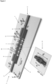
- an exemplified embodiment of the photonic crystal is based on a photonic structure created in silicon, on a silicon oxide substrate consisting of one single-mode input and another output guide, and of the bimodal periodic structure, Figure 1 .
- the input guide which supports the fundamental mode of light with transverse electric (TE) polarisation, is responsible for exciting and transmitting its power to the two propagating modes through the one-dimensional periodic structure, the fundamental mode and the higher order mode, both of even parity.
- the two modes propagated by the periodic guide will be responsible for exciting the fundamental mode of the single-mode guide at the output, whose power will depend on the phase shift produced between the two modes along the periodic structure.
- This one-dimensional periodic structure is composed of the repetition of a basic unit cell along the light propagation axis, and of a small homogeneous guide transition between the single-mode guides and the bimodal periodic structure.
- the design parameters are the periodicity a, the width of the transverse element w i , the length of the transverse element w e , the width of the central guide w and the height h, and with a width for the inlet and outlet guides w s .
- the band diagrams of the unit cell must be calculated in order to know the behaviour of the propagating modes. Only the modes of the polarisation considered (in this implementation they are considered TE), which are those that will be excited by the arranged input guides, will be computed and taken into account.
- the first band is composed of the first fundamental mode
- the second and third bands are a mixture of the first fundamental mode with the higher order mode.
- the presence of photonic band-gaps is also obtained, which are those regions in wavelength or frequency where light is not transmitted and this is totally reflected or radiated.
- the second and third bands originate by having an intersection of the first fundamental light mode folded in the irreducible Brillouin zone with the second higher order light mode.
- a unit cell has been designed with a bimodal region where actually reduced group velocities are produced for the higher order mode, thus maximising the effect and sensitivity of the interferometer.
- the transmission spectrum contains more clustered interferences for those wavelengths where the higher order mode behaves highly dispersively, as opposed to what occurs for higher wavelengths where the higher order mode is not as dispersive. It is, therefore, in this region of the spectrum where a greater number of spectral peaks occur where the interferometer will obtain its best performances.
- the placement of the homogeneous guide transition between the single-mode input guides and the periodic bimodal structure is fundamental to correctly excite both modes in the periodic structure. Without such a transition, only the fundamental mode would be excited in the periodic guide, thus losing its bimodal operation and its ability to cause signals to interfere.
- the size of the transition must be designed in order to maximise the spectral peaks produced by the bimodal interferences, such that the excitation of the higher order mode is adequate.
- the interference pattern of the transmission spectrum indicates to us that constructive interference is occurring between the two modes for peaks: a phase shift produced multiple of 2 ⁇ .
- the phase shift between the modes is a multiple of ⁇ .
- the fundamental mode acts as a reference since it accumulates a smaller phase shift by varying the optical properties of the environment, so it is the higher order mode that will act as a signal sensitive to optical variations.
- the present invention also relates to an interferometer comprising the photonic crystal defined herein.
- an interferometer comprising the photonic crystal defined herein.
- interference is generated between modes ⁇ 1 and ⁇ 2 in the crystal so that a parameter of the light emitted from the photonic crystal or the interferometer is changed.
- the photonic crystal and the integrated interferometric device of the present invention represent an ultra-compact product and highly sensitive to variations of the environment affecting the optical signal.
- it has a simple design that can be easily carried out using manufacturing processes suitable for mass production. All of this allows the implementation of this device on a chip together with other integrated optical elements, in such a way that its reduced size helps the integration of multiple designs in a reduced area.
- the present invention also relates to the use of said crystal or said interferometer as a photonic modulator, as a refractive index sensor for detecting changes in the raw index of a concentration of a compound between samples deposited on said photonic crystal or said interferometer, respectively, or as a chemical or biological substance detection sensor.
- a variation in an optical property of an object or environment in the vicinity of said photonic crystal or said interferometer is determined for said uses.
- the present invention also relates to a method for detecting a variation in an optical property of an object or environment, using the photonic crystal or the interferometer of the present invention, wherein said method comprises the following steps:
- the parameter of the emitted light is the free spectral range, measured as the distance between two maximum peaks in the spectral interference pattern at the output of the device, wherein there is a difference between the parameters of steps (i) and (ii), when the phase shift between spectral interference patterns of steps (i) and (ii) is greater than zero.
- the method comprises the further step of determining the influence of said variation by obtaining the relationship that occurs between the difference determined in step (iii), with respect to the change in the optical property of said object or environment.
- simulations of transmission spectra and field excitation were numerically calculated using the CST Microwave Studio software.
- a full-vector time domain 3D solver using finite integration techniques was used to simulate the entire interferometric system, including single-mode and bimodal waveguides.
- a hexahedral grid of 20 cells per wavelength was used for the entire structure, with silica as the background.
- the FFT Fast Fourier Transform
- the excitation of the structure was performed by standard waveguide ports at the input and output, with the aim of providing the scattering parameters.
- the photonic structures were manufactured on a silicon-on-insulator (SOI) wafer with a silicon layer thickness of 220 nm and a silica underlayer of 2 ⁇ m.
- An acceleration voltage of 30 KeV and an aperture size of 30 ⁇ m were used in the electron beam lithography process used to create the photonic structures on a negative hydrogen silsesquioxane (HSQ) resin; then, an inductively coupled plasma etch was used to transfer the designed patterns to the silicon layer.
- HSQ hydrogen silsesquioxane
- a continuous wave (CW) tunable laser (Keysight 81980) and a coherent TE polariser were used to vertically couple the light into the photonic structures by using cut optical fibers near grating couplers.
- a laser synchronised power meter (Keysight 81636B) was used to measure the response of the optical circuits.
- the transmitted spectra were recorded digitally by a LabVIEW application, also responsible for controlling the chip temperature by using a Peltier heater connected to the copper support of the photonic sample. A time period of 5 minutes after temperature changes was used to allow the sample to stabilise under the desired conditions.
- the chip was placed in a sealed container and covered with the deionised water (DIW) or increasing solutions of ethanol (EtOH) in DIW directly deposited on the sample and measured after a stabilisation time of 5 minutes.
- DIW deionised water
- EtOH increasing solutions of ethanol
- the proposed design shown in Figure 1 , is based entirely on a silicon structure surrounded by a silica cladding, where a single-mode input waveguide, supporting the fundamental mode of transverse electric polarisation (TE), transfers its power to the first two TE even modes in the bimodal region of the 1D photonic crystal: TE 0 and TE 2 . These two modes propagate through the 1D photonic crystal and, after a certain distance, interfere in the abrupt discontinuity with the single-mode output waveguide, contributing to the excitation of the fundamental TE mode at the output. Therefore, the transferred power can be expressed as a function of the accumulated phase shift between both modes in the bimodal region.
- TE transverse electric polarisation
- the bimodal interferometric structure is composed of a repetition of a basic unit cell consisting of a transverse element or corrugation on a central rectangular waveguide (see the box of Figure 1 ), creating a 1D photonic crystal in the direction of propagation of the z-axis.
- Figure 2A depicts the scatter diagram in the irreducible Brillouin zone of the designed 1D photonic crystal, showing the TE type bands that will be excited by the fundamental TE mode of the single-mode input waveguide.
- the first three bands are represented, showing in solid line and dotted line the contribution of the fundamental (TEo) and second order (TE 2 ) modes, respectively.
- the first band (I) is entirely formed by the fundamental mode, while the second and third bands (II and III) are composed of a combination of both modes. Between these two bands, a photonic band-gap (PBG) is created as a result of the anti-crossing point produced by the fundamental mode, folded into the first Brillouin zone and the higher order mode.
- PBG photonic band-gap
- the higher order mode strongly interacts with the periodic pattern of the structure, thus producing a highly dispersive behaviour of the third band at the end of the Brillouin zone.
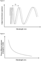
- Figure 7B shows the maximum group velocity difference between both modes in the slow light region of the higher order mode and the bandwidth of the bimodal region of interest as a function of w e .
- the group velocity difference in the region of interest increases with w e until wavelengths near the photonic band-gap are reached, where the fundamental mode is also converted to slow light.
- the bandwidth decreases due to the flattening of the higher order mode, resulting in lower wavelength bimodal regions.
- a w e value of 1400 nm was selected, as this configuration provides a large group velocity difference and a large bandwidth for this embodiment.
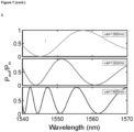
- bimodal excitation decreases for lower wavelengths, as can be seen in the shaded area of the region of interest in Figure 8A .
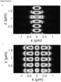
- the absolute value of the electric field in the 2D plane at the output of the bimodal interferometer is plotted without and with taper for destructive interference at 1563.5 nm in Figures 8C and D , respectively. In the absence of a rectangular taper, all energy is transferred to the single-mode output waveguide, while with a taper there is destructive interference due to adequate bimodal excitation and almost no power is transmitted to the output waveguide.
- FFT Fast Fourier Transform
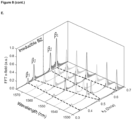
- Bimodal interferometers were manufactured with the previously detailed design parameters and a taper with a nominal length of 1200 nm at the input and output interfaces (see Figure 9A ). All the parameters of the manufactured structures perfectly match the theoretical design, except for the taper, which has a measured length of ⁇ 1400 nm. This difference is due to the fact that the taper was very close to the first transverse element of the 1D photonic crystal (with a gap of only 60 nm) and the latter was not resolved in manufacture (see Figure 9A ). Despite this deviation, the length of the manufactured taper also remains within the optimal bimodal excitation range, as can be seen in Figure 8B , so the experimental performance is not expected to be altered.
- the free spectral range (FSR) of the ripple is homogeneously distributed and is very similar to that calculated for a cavity distance on the chip of 0.9 mm ( ⁇ 1.5 nm), demonstrating that this is caused by the Fabry-Perot contribution. Furthermore, the results show the same free spectral range for the two different bimodal lengths considered, so that the ripple must be caused by an optical cavity common in both designs (i.e. the resonances between the access grating couplers).
- n g ⁇ 2 ⁇ ⁇ max ⁇ ⁇ min / 2 L ⁇ max ⁇ ⁇ min + n g ⁇ 1 ⁇
- L the length of the bimodal photonic crystal waveguide
- n g ⁇ 1 the fundamental mode group index acting as reference signal.
- the bimodal slow light interferometer exhibits a group index of up to ⁇ 23 for the higher order mode, which matches the simulations perfectly.
- the fundamental mode simulated group index that has been used in equation (1) is shown with the dotted and dashed line in Figure 9B and exhibits group index values less than 5 in the region of interest.
- phase change ⁇ which corresponds to a change of refractive index of the required silicon of 2.4 ⁇ 10 -3 .
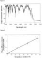
- phase shift values of ⁇ were obtained for a temperature change of 75 °C for 1550 nm interference in the 148 ⁇ m long configuration, corresponding to a required silicon change of 1.35x10⁻² RIU (see dashed lines in Figure 10D ).
- interferometers are highly efficient and have a large bandwidth, which also demonstrates a flexibility in the design based on the desired operation.
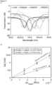
- the interferometric response is now obtained for lower wavelengths (interferences located around 1515 nm are now measured) since the DIW-based topcoat has a lower refractive index than that of silica.
- the spectrum shifts towards higher wavelengths by increasing the refractive index of the coating.
- a Lorentzian fit has been made on spectral interferences to correctly obtain the minimum peaks caused by bimodal behaviour (see Figure 11A ).
- knowing the spectral shift due to the changes of the refractive index of the coating enables calculating its corresponding phase shift using equation (2).
- Experimental sensitivity can be determined as the slope of the phase shift adjustment for different changes in the refractive index of the coating.
- Experimental values of up to 75.20 ⁇ 2 ⁇ rad/ RIU and 150.83 ⁇ 2 ⁇ rad/ RIU are obtained for a bimodal interferometer length of 74 ⁇ m and 148 ⁇ m, respectively. The results obtained clearly follow a linear evolution and present a value twice as large due to the double length used for this configuration compared to the shorter one, similarly to the previous case.
- n c is the refractive index of the coating
- L the length of the interferometer
- n eff1 and n eff2 the effective index of the fundamental and higher order mode, respectively.
- the bimodal periodic structures exemplified herein provide interferometric behaviour involving higher order modes with an extremely sensitive phase shift produced by changes induced in the refractive index. Compared to other existing bimodal configurations, this design makes use of 1D photonic crystal structures with an active mode that works in the slow light regime. This effect has been enabled by active control of the band diagrams to optimise the desired bimodal behaviour in order to improve the interferometric response. This process can be extended to 2D and 3D photonic crystals.
- the proposed device has been experimentally demonstrated for optical modulation and detection purposes, to determine its efficiency in dynamic systems.
- the interferometer response to small changes in the refractive index of the silicon structure was tested.
- a single-channel interferometer with an area of only - 100 ⁇ m 2 is provided for high-efficiency temperature modulation, improving conventional Mach-Zehnder interferometer-based structures by two orders of magnitude and improving interferometric schemes, including 2D and 1D photonic crystals by more than one order of magnitude. Because of its compact design, the results suggest the use of this type of bimodal photonic crystal silicon waveguide for the integration of multiple on-chip modulators.
Landscapes
- Physics & Mathematics (AREA)
- Nonlinear Science (AREA)
- General Physics & Mathematics (AREA)
- Optics & Photonics (AREA)
- Chemical & Material Sciences (AREA)
- Engineering & Computer Science (AREA)
- Ceramic Engineering (AREA)
- Crystallography & Structural Chemistry (AREA)
- Optical Integrated Circuits (AREA)
Applications Claiming Priority (2)
| Application Number | Priority Date | Filing Date | Title |
|---|---|---|---|
| ES202031056A ES2833462B2 (es) | 2020-10-20 | 2020-10-20 | Metodo para maximizar el desfase en una guia bimodal de cristal fotonico |
| PCT/ES2021/070761 WO2022084566A1 (es) | 2020-10-20 | 2021-10-20 | Método para maximizar el desfase en una guía bimodal de cristal fotónico |
Publications (2)
| Publication Number | Publication Date |
|---|---|
| EP4235291A1 true EP4235291A1 (de) | 2023-08-30 |
| EP4235291A4 EP4235291A4 (de) | 2024-08-21 |
Family
ID=76372255
Family Applications (1)
| Application Number | Title | Priority Date | Filing Date |
|---|---|---|---|
| EP21882217.9A Withdrawn EP4235291A4 (de) | 2020-10-20 | 2021-10-20 | Verfahren zur maximierung der phasenverschiebung in einem bimodalen photonischen kristallleiter |
Country Status (4)
| Country | Link |
|---|---|
| US (1) | US20230393425A1 (de) |
| EP (1) | EP4235291A4 (de) |
| ES (1) | ES2833462B2 (de) |
| WO (1) | WO2022084566A1 (de) |
Families Citing this family (1)
| Publication number | Priority date | Publication date | Assignee | Title |
|---|---|---|---|---|
| CN119694858B (zh) * | 2024-12-06 | 2025-11-11 | 北京真空电子技术研究所(中国电子科技集团公司第十二研究所) | 一种双峰双曲余弦波导慢波结构、行波管及设计方法 |
Family Cites Families (3)
| Publication number | Priority date | Publication date | Assignee | Title |
|---|---|---|---|---|
| CN104018294B (zh) * | 2014-04-10 | 2016-06-22 | 中国科学院宁波材料技术与工程研究所 | 一种聚乳酸纳米纤维膜及其制备方法 |
| WO2017180217A1 (en) * | 2016-04-15 | 2017-10-19 | Northwestern University | X(2) modulators and related devices with barium titanate photonic crystal waveguides |
| US10490906B2 (en) * | 2017-08-22 | 2019-11-26 | Omega Optics, Inc. | Slot waveguide with structural modulation |
-
2020
- 2020-10-20 ES ES202031056A patent/ES2833462B2/es active Active
-
2021
- 2021-10-20 US US18/248,923 patent/US20230393425A1/en not_active Abandoned
- 2021-10-20 WO PCT/ES2021/070761 patent/WO2022084566A1/es not_active Ceased
- 2021-10-20 EP EP21882217.9A patent/EP4235291A4/de not_active Withdrawn
Also Published As
| Publication number | Publication date |
|---|---|
| ES2833462A1 (es) | 2021-06-15 |
| US20230393425A1 (en) | 2023-12-07 |
| WO2022084566A1 (es) | 2022-04-28 |
| EP4235291A4 (de) | 2024-08-21 |
| ES2833462B2 (es) | 2022-12-14 |
Similar Documents
| Publication | Publication Date | Title |
|---|---|---|
| Torrijos-Morán et al. | Slow light bimodal interferometry in one-dimensional photonic crystal waveguides | |
| Han et al. | Guided‐mode resonances in all‐dielectric terahertz metasurfaces | |
| Canós Valero et al. | Exceptional bound states in the continuum | |
| Wang | Silicon photonic waveguide Bragg gratings | |
| JP5588794B2 (ja) | グレーティング構造を有する基板型光導波路素子、波長分散補償素子および基板型光導波路素子の製造方法 | |
| Sun et al. | Large group delay in silicon-on-insulator chirped spiral Bragg grating waveguide | |
| Charlton et al. | Experimental investigation of photonic crystal waveguide devices and line-defect waveguide bends | |
| Chen et al. | Relaxed-tolerance subwavelength grating coupler | |
| EP4235291A1 (de) | Verfahren zur maximierung der phasenverschiebung in einem bimodalen photonischen kristallleiter | |
| Ciminelli et al. | Modeling and design of two-dimensional guided-wave photonic band-gap devices | |
| Safaee et al. | Silicon photonics mode-selective phase shifter | |
| Dong et al. | Polarization-selective high-sensitivity Fano resonance in all-dielectric metasurface based on quasi-bound states in the continuum | |
| Cucinotta et al. | Impact of the cell geometry on the spectral properties of photonic crystal structures | |
| Han | Terahertz bound states in the continuum | |
| Liu et al. | Terahertz interface states in a heterostructure parallel plate waveguide | |
| Němec et al. | Transmission properties and band structure of a segmented dielectric waveguide for the terahertz range | |
| Al Qubaisi | Toward an Active CMOS Electronics-Photonics Platform Based on Subwavelength Structured Devices | |
| BLATCHER | Engineering Periodic Structures in Dielectric Waveguides for Quantum Applications | |
| Herrero-Parareda et al. | Frozen mode in coupled single-mode waveguides with gratings | |
| González et al. | Breakthrough silicon photonics devices using subwavelength grating metamaterials | |
| Dubey et al. | High-Performance Silicon Nitride Waveguides: A Platform for Nonlinear and Quantum Photonics | |
| Furman | Towards the Realization of the Stationary Inflection Point in Silicon Photonics and Its Applications | |
| Wang et al. | Silicon photonic Bragg gratings | |
| Pant | Low power optical phase shifter devices | |
| Sun | Waveguide Bragg gratings using subwavelength grating waveguide in silicon photonics platform |
Legal Events
| Date | Code | Title | Description |
|---|---|---|---|
| STAA | Information on the status of an ep patent application or granted ep patent |
Free format text: STATUS: THE INTERNATIONAL PUBLICATION HAS BEEN MADE |
|
| PUAI | Public reference made under article 153(3) epc to a published international application that has entered the european phase |
Free format text: ORIGINAL CODE: 0009012 |
|
| STAA | Information on the status of an ep patent application or granted ep patent |
Free format text: STATUS: REQUEST FOR EXAMINATION WAS MADE |
|
| 17P | Request for examination filed |
Effective date: 20230504 |
|
| AK | Designated contracting states |
Kind code of ref document: A1 Designated state(s): AL AT BE BG CH CY CZ DE DK EE ES FI FR GB GR HR HU IE IS IT LI LT LU LV MC MK MT NL NO PL PT RO RS SE SI SK SM TR |
|
| DAV | Request for validation of the european patent (deleted) | ||
| DAX | Request for extension of the european patent (deleted) | ||
| A4 | Supplementary search report drawn up and despatched |
Effective date: 20240722 |
|
| RIC1 | Information provided on ipc code assigned before grant |
Ipc: G02F 1/03 20060101ALI20240716BHEP Ipc: G02F 1/225 20060101AFI20240716BHEP |
|
| STAA | Information on the status of an ep patent application or granted ep patent |
Free format text: STATUS: THE APPLICATION IS DEEMED TO BE WITHDRAWN |
|
| 18D | Application deemed to be withdrawn |
Effective date: 20250211 |