EP4231524A2 - Power amplifier using multi-path common-mode feedback loop - Google Patents
Power amplifier using multi-path common-mode feedback loop Download PDFInfo
- Publication number
- EP4231524A2 EP4231524A2 EP23154128.5A EP23154128A EP4231524A2 EP 4231524 A2 EP4231524 A2 EP 4231524A2 EP 23154128 A EP23154128 A EP 23154128A EP 4231524 A2 EP4231524 A2 EP 4231524A2
- Authority
- EP
- European Patent Office
- Prior art keywords
- power amplifier
- amplifier stage
- pfet
- gate
- coupled
- Prior art date
- Legal status (The legal status is an assumption and is not a legal conclusion. Google has not performed a legal analysis and makes no representation as to the accuracy of the status listed.)
- Pending
Links
- 230000005669 field effect Effects 0.000 claims abstract description 13
- 230000000295 complement effect Effects 0.000 claims abstract description 10
- 229910044991 metal oxide Inorganic materials 0.000 abstract description 6
- 150000004706 metal oxides Chemical class 0.000 abstract description 6
- 239000004065 semiconductor Substances 0.000 abstract description 6
- 238000010586 diagram Methods 0.000 description 19
- 239000003990 capacitor Substances 0.000 description 14
- 238000000034 method Methods 0.000 description 10
- 230000008569 process Effects 0.000 description 5
- 238000012545 processing Methods 0.000 description 5
- 238000010295 mobile communication Methods 0.000 description 4
- 238000005516 engineering process Methods 0.000 description 3
- 230000005540 biological transmission Effects 0.000 description 2
- 238000012937 correction Methods 0.000 description 2
- 238000013461 design Methods 0.000 description 2
- 239000000284 extract Substances 0.000 description 2
- 230000006872 improvement Effects 0.000 description 2
- 239000000243 solution Substances 0.000 description 2
- 239000000758 substrate Substances 0.000 description 2
- JBRZTFJDHDCESZ-UHFFFAOYSA-N AsGa Chemical compound [As]#[Ga] JBRZTFJDHDCESZ-UHFFFAOYSA-N 0.000 description 1
- 238000013459 approach Methods 0.000 description 1
- 230000001413 cellular effect Effects 0.000 description 1
- 238000004891 communication Methods 0.000 description 1
- 230000001143 conditioned effect Effects 0.000 description 1
- 230000008878 coupling Effects 0.000 description 1
- 238000010168 coupling process Methods 0.000 description 1
- 238000005859 coupling reaction Methods 0.000 description 1
- 230000001419 dependent effect Effects 0.000 description 1
- 230000000694 effects Effects 0.000 description 1
- 238000001914 filtration Methods 0.000 description 1
- 230000006870 function Effects 0.000 description 1
- 238000002347 injection Methods 0.000 description 1
- 239000007924 injection Substances 0.000 description 1
- 238000002955 isolation Methods 0.000 description 1
- 239000000463 material Substances 0.000 description 1
- 238000012986 modification Methods 0.000 description 1
- 230000004048 modification Effects 0.000 description 1
- 230000001737 promoting effect Effects 0.000 description 1
- 239000007787 solid Substances 0.000 description 1
- 230000001052 transient effect Effects 0.000 description 1
Images






Classifications
-
- H—ELECTRICITY
- H03—ELECTRONIC CIRCUITRY
- H03F—AMPLIFIERS
- H03F3/00—Amplifiers with only discharge tubes or only semiconductor devices as amplifying elements
- H03F3/20—Power amplifiers, e.g. Class B amplifiers, Class C amplifiers
- H03F3/21—Power amplifiers, e.g. Class B amplifiers, Class C amplifiers with semiconductor devices only
-
- H—ELECTRICITY
- H03—ELECTRONIC CIRCUITRY
- H03F—AMPLIFIERS
- H03F3/00—Amplifiers with only discharge tubes or only semiconductor devices as amplifying elements
- H03F3/45—Differential amplifiers
- H03F3/45071—Differential amplifiers with semiconductor devices only
- H03F3/45479—Differential amplifiers with semiconductor devices only characterised by the way of common mode signal rejection
- H03F3/45632—Differential amplifiers with semiconductor devices only characterised by the way of common mode signal rejection in differential amplifiers with FET transistors as the active amplifying circuit
- H03F3/45636—Differential amplifiers with semiconductor devices only characterised by the way of common mode signal rejection in differential amplifiers with FET transistors as the active amplifying circuit by using feedback means
-
- H—ELECTRICITY
- H03—ELECTRONIC CIRCUITRY
- H03F—AMPLIFIERS
- H03F3/00—Amplifiers with only discharge tubes or only semiconductor devices as amplifying elements
- H03F3/20—Power amplifiers, e.g. Class B amplifiers, Class C amplifiers
- H03F3/24—Power amplifiers, e.g. Class B amplifiers, Class C amplifiers of transmitter output stages
- H03F3/245—Power amplifiers, e.g. Class B amplifiers, Class C amplifiers of transmitter output stages with semiconductor devices only
-
- H—ELECTRICITY
- H03—ELECTRONIC CIRCUITRY
- H03F—AMPLIFIERS
- H03F1/00—Details of amplifiers with only discharge tubes, only semiconductor devices or only unspecified devices as amplifying elements
- H03F1/02—Modifications of amplifiers to raise the efficiency, e.g. gliding Class A stages, use of an auxiliary oscillation
- H03F1/0205—Modifications of amplifiers to raise the efficiency, e.g. gliding Class A stages, use of an auxiliary oscillation in transistor amplifiers
- H03F1/0211—Modifications of amplifiers to raise the efficiency, e.g. gliding Class A stages, use of an auxiliary oscillation in transistor amplifiers with control of the supply voltage or current
- H03F1/0216—Continuous control
- H03F1/0222—Continuous control by using a signal derived from the input signal
-
- H—ELECTRICITY
- H03—ELECTRONIC CIRCUITRY
- H03F—AMPLIFIERS
- H03F1/00—Details of amplifiers with only discharge tubes, only semiconductor devices or only unspecified devices as amplifying elements
- H03F1/02—Modifications of amplifiers to raise the efficiency, e.g. gliding Class A stages, use of an auxiliary oscillation
- H03F1/0205—Modifications of amplifiers to raise the efficiency, e.g. gliding Class A stages, use of an auxiliary oscillation in transistor amplifiers
- H03F1/0261—Modifications of amplifiers to raise the efficiency, e.g. gliding Class A stages, use of an auxiliary oscillation in transistor amplifiers with control of the polarisation voltage or current, e.g. gliding Class A
- H03F1/0266—Modifications of amplifiers to raise the efficiency, e.g. gliding Class A stages, use of an auxiliary oscillation in transistor amplifiers with control of the polarisation voltage or current, e.g. gliding Class A by using a signal derived from the input signal
-
- H—ELECTRICITY
- H03—ELECTRONIC CIRCUITRY
- H03F—AMPLIFIERS
- H03F1/00—Details of amplifiers with only discharge tubes, only semiconductor devices or only unspecified devices as amplifying elements
- H03F1/08—Modifications of amplifiers to reduce detrimental influences of internal impedances of amplifying elements
- H03F1/22—Modifications of amplifiers to reduce detrimental influences of internal impedances of amplifying elements by use of cascode coupling, i.e. earthed cathode or emitter stage followed by earthed grid or base stage respectively
- H03F1/223—Modifications of amplifiers to reduce detrimental influences of internal impedances of amplifying elements by use of cascode coupling, i.e. earthed cathode or emitter stage followed by earthed grid or base stage respectively with MOSFET's
-
- H—ELECTRICITY
- H03—ELECTRONIC CIRCUITRY
- H03F—AMPLIFIERS
- H03F1/00—Details of amplifiers with only discharge tubes, only semiconductor devices or only unspecified devices as amplifying elements
- H03F1/38—Positive-feedback circuit arrangements without negative feedback
-
- H—ELECTRICITY
- H03—ELECTRONIC CIRCUITRY
- H03F—AMPLIFIERS
- H03F3/00—Amplifiers with only discharge tubes or only semiconductor devices as amplifying elements
- H03F3/189—High-frequency amplifiers, e.g. radio frequency amplifiers
- H03F3/19—High-frequency amplifiers, e.g. radio frequency amplifiers with semiconductor devices only
- H03F3/193—High-frequency amplifiers, e.g. radio frequency amplifiers with semiconductor devices only with field-effect devices
-
- H—ELECTRICITY
- H03—ELECTRONIC CIRCUITRY
- H03F—AMPLIFIERS
- H03F3/00—Amplifiers with only discharge tubes or only semiconductor devices as amplifying elements
- H03F3/26—Push-pull amplifiers; Phase-splitters therefor
- H03F3/265—Push-pull amplifiers; Phase-splitters therefor with field-effect transistors only
-
- H—ELECTRICITY
- H03—ELECTRONIC CIRCUITRY
- H03F—AMPLIFIERS
- H03F3/00—Amplifiers with only discharge tubes or only semiconductor devices as amplifying elements
- H03F3/30—Single-ended push-pull [SEPP] amplifiers; Phase-splitters therefor
- H03F3/3001—Single-ended push-pull [SEPP] amplifiers; Phase-splitters therefor with field-effect transistors
- H03F3/3022—CMOS common source output SEPP amplifiers
-
- H—ELECTRICITY
- H03—ELECTRONIC CIRCUITRY
- H03F—AMPLIFIERS
- H03F3/00—Amplifiers with only discharge tubes or only semiconductor devices as amplifying elements
- H03F3/45—Differential amplifiers
- H03F3/45071—Differential amplifiers with semiconductor devices only
- H03F3/45076—Differential amplifiers with semiconductor devices only characterised by the way of implementation of the active amplifying circuit in the differential amplifier
- H03F3/45179—Differential amplifiers with semiconductor devices only characterised by the way of implementation of the active amplifying circuit in the differential amplifier using MOSFET transistors as the active amplifying circuit
- H03F3/45224—Complementary Pl types having parallel inputs and being supplied in parallel
- H03F3/45228—Non-folded cascode stages
-
- H—ELECTRICITY
- H03—ELECTRONIC CIRCUITRY
- H03F—AMPLIFIERS
- H03F3/00—Amplifiers with only discharge tubes or only semiconductor devices as amplifying elements
- H03F3/45—Differential amplifiers
- H03F3/45071—Differential amplifiers with semiconductor devices only
- H03F3/45479—Differential amplifiers with semiconductor devices only characterised by the way of common mode signal rejection
- H03F3/45632—Differential amplifiers with semiconductor devices only characterised by the way of common mode signal rejection in differential amplifiers with FET transistors as the active amplifying circuit
- H03F3/45636—Differential amplifiers with semiconductor devices only characterised by the way of common mode signal rejection in differential amplifiers with FET transistors as the active amplifying circuit by using feedback means
- H03F3/45641—Measuring at the loading circuit of the differential amplifier
- H03F3/45654—Controlling the active amplifying circuit of the differential amplifier
-
- H—ELECTRICITY
- H04—ELECTRIC COMMUNICATION TECHNIQUE
- H04B—TRANSMISSION
- H04B1/00—Details of transmission systems, not covered by a single one of groups H04B3/00 - H04B13/00; Details of transmission systems not characterised by the medium used for transmission
- H04B1/38—Transceivers, i.e. devices in which transmitter and receiver form a structural unit and in which at least one part is used for functions of transmitting and receiving
- H04B1/40—Circuits
-
- H—ELECTRICITY
- H03—ELECTRONIC CIRCUITRY
- H03F—AMPLIFIERS
- H03F2200/00—Indexing scheme relating to amplifiers
- H03F2200/171—A filter circuit coupled to the output of an amplifier
-
- H—ELECTRICITY
- H03—ELECTRONIC CIRCUITRY
- H03F—AMPLIFIERS
- H03F2200/00—Indexing scheme relating to amplifiers
- H03F2200/451—Indexing scheme relating to amplifiers the amplifier being a radio frequency amplifier
-
- H—ELECTRICITY
- H03—ELECTRONIC CIRCUITRY
- H03F—AMPLIFIERS
- H03F2200/00—Indexing scheme relating to amplifiers
- H03F2200/474—A current mirror being used as sensor
-
- H—ELECTRICITY
- H03—ELECTRONIC CIRCUITRY
- H03F—AMPLIFIERS
- H03F2203/00—Indexing scheme relating to amplifiers with only discharge tubes or only semiconductor devices as amplifying elements covered by H03F3/00
- H03F2203/30—Indexing scheme relating to single-ended push-pull [SEPP]; Phase-splitters therefor
- H03F2203/30021—A capacitor being coupled in a feedback circuit of a SEPP amplifier
-
- H—ELECTRICITY
- H03—ELECTRONIC CIRCUITRY
- H03F—AMPLIFIERS
- H03F2203/00—Indexing scheme relating to amplifiers with only discharge tubes or only semiconductor devices as amplifying elements covered by H03F3/00
- H03F2203/30—Indexing scheme relating to single-ended push-pull [SEPP]; Phase-splitters therefor
- H03F2203/30027—Indexing scheme relating to single-ended push-pull [SEPP]; Phase-splitters therefor the SEPP bias voltage being controlled by a control signal from a feedback circuit
-
- H—ELECTRICITY
- H03—ELECTRONIC CIRCUITRY
- H03F—AMPLIFIERS
- H03F2203/00—Indexing scheme relating to amplifiers with only discharge tubes or only semiconductor devices as amplifying elements covered by H03F3/00
- H03F2203/30—Indexing scheme relating to single-ended push-pull [SEPP]; Phase-splitters therefor
- H03F2203/30036—A feedback circuit to stabilise the SEPP being used
-
- H—ELECTRICITY
- H03—ELECTRONIC CIRCUITRY
- H03F—AMPLIFIERS
- H03F2203/00—Indexing scheme relating to amplifiers with only discharge tubes or only semiconductor devices as amplifying elements covered by H03F3/00
- H03F2203/30—Indexing scheme relating to single-ended push-pull [SEPP]; Phase-splitters therefor
- H03F2203/30054—Indexing scheme relating to single-ended push-pull [SEPP]; Phase-splitters therefor the SEPP power transistors are realised as paralleled cascode coupled transistors, i.e. the push or the pull transistors
-
- H—ELECTRICITY
- H03—ELECTRONIC CIRCUITRY
- H03F—AMPLIFIERS
- H03F2203/00—Indexing scheme relating to amplifiers with only discharge tubes or only semiconductor devices as amplifying elements covered by H03F3/00
- H03F2203/30—Indexing scheme relating to single-ended push-pull [SEPP]; Phase-splitters therefor
- H03F2203/30057—Indexing scheme relating to single-ended push-pull [SEPP]; Phase-splitters therefor the SEPP power transistors are realised as paralleled FETs, i.e. the push or the pull transistor
-
- H—ELECTRICITY
- H03—ELECTRONIC CIRCUITRY
- H03F—AMPLIFIERS
- H03F2203/00—Indexing scheme relating to amplifiers with only discharge tubes or only semiconductor devices as amplifying elements covered by H03F3/00
- H03F2203/30—Indexing scheme relating to single-ended push-pull [SEPP]; Phase-splitters therefor
- H03F2203/30084—Indexing scheme relating to single-ended push-pull [SEPP]; Phase-splitters therefor the pull circuit of the SEPP amplifier being a cascode circuit
-
- H—ELECTRICITY
- H03—ELECTRONIC CIRCUITRY
- H03F—AMPLIFIERS
- H03F2203/00—Indexing scheme relating to amplifiers with only discharge tubes or only semiconductor devices as amplifying elements covered by H03F3/00
- H03F2203/30—Indexing scheme relating to single-ended push-pull [SEPP]; Phase-splitters therefor
- H03F2203/30117—Indexing scheme relating to single-ended push-pull [SEPP]; Phase-splitters therefor the push circuit of the SEPP amplifier being a cascode circuit
-
- H—ELECTRICITY
- H03—ELECTRONIC CIRCUITRY
- H03F—AMPLIFIERS
- H03F2203/00—Indexing scheme relating to amplifiers with only discharge tubes or only semiconductor devices as amplifying elements covered by H03F3/00
- H03F2203/45—Indexing scheme relating to differential amplifiers
- H03F2203/45084—Indexing scheme relating to differential amplifiers the common mode signal circuit comprising one or more inductive or capacitive elements, e.g. filter circuitry
-
- H—ELECTRICITY
- H03—ELECTRONIC CIRCUITRY
- H03F—AMPLIFIERS
- H03F2203/00—Indexing scheme relating to amplifiers with only discharge tubes or only semiconductor devices as amplifying elements covered by H03F3/00
- H03F2203/45—Indexing scheme relating to differential amplifiers
- H03F2203/45404—Indexing scheme relating to differential amplifiers the CMCL comprising capacitors containing, not in parallel with the resistors, an addition circuit
-
- H—ELECTRICITY
- H03—ELECTRONIC CIRCUITRY
- H03F—AMPLIFIERS
- H03F2203/00—Indexing scheme relating to amplifiers with only discharge tubes or only semiconductor devices as amplifying elements covered by H03F3/00
- H03F2203/45—Indexing scheme relating to differential amplifiers
- H03F2203/45418—Indexing scheme relating to differential amplifiers the CMCL comprising a resistor addition circuit
-
- H—ELECTRICITY
- H03—ELECTRONIC CIRCUITRY
- H03F—AMPLIFIERS
- H03F2203/00—Indexing scheme relating to amplifiers with only discharge tubes or only semiconductor devices as amplifying elements covered by H03F3/00
- H03F2203/45—Indexing scheme relating to differential amplifiers
- H03F2203/45422—Indexing scheme relating to differential amplifiers the CMCL comprising one or more capacitors not as integrating capacitor, e.g. for stability purposes
-
- H—ELECTRICITY
- H03—ELECTRONIC CIRCUITRY
- H03F—AMPLIFIERS
- H03F2203/00—Indexing scheme relating to amplifiers with only discharge tubes or only semiconductor devices as amplifying elements covered by H03F3/00
- H03F2203/45—Indexing scheme relating to differential amplifiers
- H03F2203/45434—Indexing scheme relating to differential amplifiers the CMCL output control signal being a voltage signal
-
- H—ELECTRICITY
- H03—ELECTRONIC CIRCUITRY
- H03F—AMPLIFIERS
- H03F2203/00—Indexing scheme relating to amplifiers with only discharge tubes or only semiconductor devices as amplifying elements covered by H03F3/00
- H03F2203/45—Indexing scheme relating to differential amplifiers
- H03F2203/45544—Indexing scheme relating to differential amplifiers the IC comprising one or more capacitors, e.g. coupling capacitors
Definitions
- the technology of the disclosure relates generally to power amplifiers and more particularly, to complementary metal oxide semiconductor (CMOS) power amplifiers with a feedback loop.
- CMOS complementary metal oxide semiconductor
- CMOS complementary metal oxide semiconductor
- FETs field effect transistors
- PFETs cascoded p-type FETs
- a further feedback network may be associated with the supply voltage to assist in providing a symmetrical supply signal.
- the symmetrical supply signal allows for supply variations without introducing distortion for the power amplifier stage. This arrangement provides linear operation over temperature corners, process corners, supply voltage corners, and the like.
- a power amplifier stage comprises an input.
- the power amplifier stage also comprises an output.
- the power amplifier stage also comprises at least one amplifying device.
- the power amplifier stage also comprises a bias circuit.
- the power amplifier stage also comprises a common-mode feedback loop coupled to the output and the bias circuit.
- the common-mode feedback loop comprises a voltage sensor configured to sense a common-mode voltage at the output, wherein respective bias signals are based on the sensed common-mode voltage.
- the power amplifier stage also comprises at least one asymmetric dynamic feedback circuit coupled from the output of the power amplifier stage to at least one bias terminal of the power amplifier stage.
- a power amplifier stage comprises an input.
- the power amplifier stage also comprises an output.
- the power amplifier stage also comprises a common-mode supply input.
- the power amplifier stage also comprises a supply circuit that has insufficient bandwidth for a given radio frequency (RF) signal modulation bandwidth.
- the power amplifier stage also comprises a supply current sensing circuit that extracts an envelope component of a supply current.
- the power amplifier stage also comprises a fast feed-forward branch that bypasses the supply circuit with the insufficient bandwidth, by providing a high-frequency supply current for the power amplifier stage.
- a power amplifier stage comprises an input.
- the power amplifier stage also comprises an output.
- the power amplifier stage also comprises a common-mode supply circuit with insufficient bandwidth.
- the power amplifier stage also comprises a bias circuit coupled to a first gate and coupled to a second gate.
- the bias circuit is configured to bias dynamically the first gate and the second gate with respective bias signals.
- the power amplifier stage also comprises a bias feedback loop coupled to the output and the bias circuit.
- the bias feedback loop comprises a voltage sensor configured to sense voltage at the output, wherein the respective bias signals are based on the sensed voltage.
- the power amplifier stage also comprises a common-mode supply feed-forward path comprising a current sensor configured to sense a high-frequency envelope current of the power amplifier stage and inject a properly-scaled current back into a power amplifier supply line to bypass the common-mode supply circuit with the insufficient bandwidth.
- a power amplifier stage comprises an input.
- the power amplifier stage also comprises an output.
- the power amplifier stage also comprises a first NFET comprising a first gate.
- the first NFET is coupled to the input and the output.
- the power amplifier stage also comprises a first PFET comprising a second gate.
- the first PFET is coupled to the input and the output.
- the power amplifier stage also comprises a bias circuit coupled to the first gate and coupled to the second gate.
- the bias circuit is configured to bias dynamically the first gate and the second gate with respective bias signals.
- the power amplifier stage also comprises a feedback loop coupled to the output and the bias circuit.
- the feedback loop comprises a voltage sensor configured to sense voltage at the output, wherein the respective bias signals are based on the sensed voltage.
- a power amplifier stage in another aspect, comprises an input.
- the power amplifier stage also comprises an output.
- the power amplifier stage also comprises a common-mode supply input.
- the power amplifier stage also comprises a first NFET comprising a first gate.
- the first NFET is coupled to the input and the output.
- the power amplifier stage also comprises a first PFET comprising a second gate.
- the first PFET is coupled to the input and the output and the common-mode supply input.
- the power amplifier stage also comprises a feedback loop comprising a current sensor configured to sense current for the first PFET and adjust a signal from the common-mode supply input based on the sensed current.
- a power amplifier stage comprises an input.
- the power amplifier stage also comprises an output.
- the power amplifier stage also comprises a common-mode supply input.
- the power amplifier stage also comprises a first NFET comprising a first gate.
- the first NFET is coupled to the input and the output.
- the power amplifier stage also comprises a first PFET comprising a second gate.
- the first PFET is coupled to the input and the output.
- the power amplifier stage also comprises a bias circuit coupled to the first gate and coupled to the second gate.
- the bias circuit is configured to bias dynamically the first gate and the second gate with respective bias signals.
- the power amplifier stage also comprises a bias feedback loop coupled to the output and the bias circuit.
- the bias feedback loop comprises a voltage sensor configured to sense voltage at the output, wherein the respective bias signals are based on the sensed voltage.
- the power amplifier stage also comprises a common-mode supply feedback loop comprising a current sensor configured to sense current for the first PFET and adjust a signal from the common-mode supply input based on the sensed current.
- CMOS complementary metal oxide semiconductor
- FETs cascoded n-type field effect transistors
- PFETs cascoded p-type FETs
- a further feedback network may be associated with the supply voltage to assist in providing a symmetrical supply signal.
- the symmetrical supply signal allows for supply variations without introducing distortion for the power amplifier stage. This arrangement provides linear operation over temperature corners, process corners, supply voltage corners, and the like.
- a power amplifier might use a hybrid approach, where the power amplifier proper might be implemented in bipolar technologies using a material such as Gallium Arsenide (GaAs).
- the power amplifier might be controlled by a CMOS stage that has a driver amplifier, biasing circuitry, and the like. While effective at providing an acceptable cost-performance compromise while allowing tunability through, for example, a matching network and/or load line, such systems are complex and have a relatively long design cycle.
- Moving to a power amplifier that implements both the power amplifier as well as the control circuit in CMOS technology generally relies on nanometer CMOS processes.
- Such devices, and particularly the FETs of such devices can tolerate maximum voltages much lower than typical battery voltage levels. Accordingly, such devices may rely on cascode structures, where FETs are stacked relative to one another.
- FIG. 1 illustrates a block diagram of a power amplifier stage 100 that has two common-mode inputs, which impact linearity.
- a voltage source 102 e.g., VBATT
- the power amplifier 104 also receives a common-mode bias signal from a bias circuit 106. Further, the power amplifier 104 receives an RF input signal (RFin) and provides an RF output signal (RFout). Maintaining linearity while using these two common-mode inputs provides opportunities for improvement.
- RFin RF input signal
- RFout RF output signal
- aspects of the present disclosure provide two complimentary ways which singly or together help provide linearity for the power amplifier stage.
- aspects of a first of the complimentary ways of the present disclosure provide bias voltages that are dynamically varying with the signal power to keep the output common-mode fixed around a half-supply level, while the small-signal and large-signal transconductances of the FETs are kept balanced. This arrangement provides linear operation over temperature corners, process corners, supply voltage corners, and the like.
- Figure 2 illustrates a power amplifier stage 200 that has a common-mode supply correction or feedback loop 202 that modifies a supply voltage signal 204 provided to a power amplifier 206 from a voltage supply 208 (e.g., VBATT).
- a common-mode bias circuit 210 is not modified in the power amplifier stage 200 and is substantially similar to the bias circuit 106 of Figure 1 .
- the common-mode supply feedback loop 202 includes a current sensing circuit 212 and an envelope filter circuit 214. More details are provided below with reference to Figures 15-18 . It should be appreciated that the current sensing is done indirectly as indicated by the loop feeding into the current sensing circuit 212.
- Figure 3 illustrates a power amplifier stage 300 that has a common-mode bias correction or feedback loop 302 that modifies a common-mode bias signal from a bias circuit 304 to a power amplifier 306.
- the power amplifier 306 receives a common-mode supply voltage signal from a voltage supply 308.
- the common-mode bias feedback loop 302 includes a common-mode voltage sensor 310 that measures the common-mode voltage of the output port RFout.
- the common-mode bias feedback loop 302 also includes an asymmetric dynamic signal to help balance the transconductances.
- a power amplifier stage 400 illustrated in Figure 4 includes both the common-mode supply feedback loop 202 and the common-mode bias feedback loop 302 with a power amplifier 402.
- Figure 5A illustrates explicitly a single-ended power amplifier stage 500
- Figure 5B illustrates a differential power amplifier stage 550
- the concepts of the present disclosure may be extended to quadrature power amplifier stages (not shown) and Doherty, barely Doherty, out-phasing, and the like (also not shown) without departing from the present disclosure.
- the single-ended power amplifier stage 500 includes a CMOS power amplifier 502 having NFETs 504 and PFETs 506.
- the common-mode supply feedback loop 202 is provided above the PFETs 506 (i.e., between VBATT 508 and a PFET 506).
- the common-mode bias feedback loop 302 works with bias circuit 304' to provide multiple bias signals to the NFETs 504 and the PFETs 506. Again, it should be appreciated that the current sensing of the common-mode supply feedback loop 202 is indirect.
- the differential power amplifier stage 550 includes two CMOS power amplifier stacks 552(1), 552(1) having NFETs 554N, 556N and PFETs 554P, 556P.
- the common-mode supply feedback loop 202 is provided above the PFETs 554P and 556P.
- the common-mode bias feedback loop 302 works with a bias circuit 304" to provide multiple bias signals to the NFETs 554N, 556N and PFETs 554P, 556P. Again, it should be appreciated that the current sensing of the common-mode supply feedback loop 202 is indirect.
- the common-mode bias feedback loop 302 may be implemented in a simple CMOS power amplifier stage 600 as loop 602.
- the power amplifier stage 600 may include a FET stack 604 including a PFET 606 and an NFET 608.
- the FET stack 604 may couple to a supply 610 and receive an input signal (RFin) from an input node 612 while providing an output signal (RFout) at an output node 614.
- the input node 612 may be coupled to gates 606G, 608G of the FETs 606, 608 through capacitors 616, 618, respectively.
- the output node 614 may be coupled to resistors 620, 622, which couple to a bias circuit 624.
- the bias circuit 624 may include a first variable source 626 and a second variable source 628 that are controlled based on the signal from the output node 614.
- the variable sources 626, 628 provide bias signals to the gates 606G, 608G, respectively, through respective resistors 630, 632.
- the common-mode voltage at the output node 614 may be kept at about half the supply voltage from the supply 610.
- CMOS power amplifier stage 600 While effective, the CMOS power amplifier stage 600 is limited in that the total swing is limited by the single NFET 608 and single PFET 606. More commonly, a CMOS power amplifier stage will have cascoded FETs as shown in power amplifier stage 700 illustrated in Figure 7 .
- the power amplifier stage 700 includes a loop 702, analogous to the loop 602 of Figure 6 , but accommodating a cascoded FET stack 704.
- the cascoded FET stack 704 includes PFETs 706(1), 706(2) and NFETs 708(1), 708(2).
- the FET stack 704 may couple to a supply 710 and receive an input signal (RFin) from an input node 712 while providing an output signal (RFout) at an output node 714.
- the input node 712 may be coupled to gates 706G, 708G of the FETs 706(1), 708(1) through capacitors 716, 718, respectively.
- the output node 714 may be coupled to resistors 720, 722, which couple to a bias circuit 724.
- the bias circuit 724 may include a first variable source 726 and a second variable source 728 that are controlled based on the signal from the output node 714.
- the variable sources 726, 728 provide bias signals to the gates 706G, 708G, respectively, through respective resistors 730, 732.
- Controlling the bias of the FETs 706(1), 708(1) may be insufficient to hold the output node at about half the supply. Accordingly, it may be appropriate also to bias the cascoded devices in the amplifier stack as illustrated by power amplifier stage 800 in Figure 8 .
- the power amplifier stage 800 includes a loop 802, analogous to the loop 602 of Figure 6 , but accommodating a cascoded FET stack 804.
- the cascoded FET stack 804 includes PFETs 806(1), 806(2) and NFETs 808(1), 808(2).
- the FET stack 804 may couple to a supply 810 and receive an input signal (RFin) from an input node 812 while providing an output signal (RFout) at an output node 814.
- the input node 812 may be coupled to gates 806(1)G, 808(1)G of the FETs 806(1), 808(1) through capacitors 816, 818, respectively.
- the output node 814 may be coupled to resistors 820, 822, which couple to a bias circuit 824.
- the bias circuit 824 may include a first variable source 826 and a second variable source 828 that are controlled based on the signal from the output node 814.
- the variable sources 826, 828 provide bias signals to the gates 806(1)G, 808(1)G, respectively, through respective resistors 830, 832. Additional bias signals may be provided from the variable sources 826, 828 to gates 806(2)G, 808(2)G through resistors 834, 836.
- the signal at the output node 814 may be kept at about half the supply voltage from the supply 810. Note that while only one cascoded FET is shown on each half of the stack 804, the concept may be extended to larger cascoded stacks without departing from the present disclosure.
- the power amplifier stage 900 includes loop 902, analogous to the loop 602 of Figure 6 , but accommodating a cascoded FET stack 904.
- the cascoded FET stack 904 includes PFETs 906(1), 906(2) and NFETs 908(1), 908(2).
- the FET stack 904 may couple to a supply 910 and receive an input signal (RFin) from an input node 912 while providing an output signal (RFout) at an output node 914.
- the input node 912 may be coupled to gates 906(1)G, 908(1)G of the FETs 906(1), 908(1) through capacitors 916, 918, respectively.
- the output node 914 may be coupled to resistors 920, 922, which couple to a bias circuit 924.
- the bias circuit 924 may include a first variable source 926 and a second variable source 928 that are controlled based on the signal from the output node 914.
- the variable sources 926, 928 provide bias signals to the gates 906(1)G, 908(1)G, respectively, through respective resistors 930, 932. Additional bias signals may be provided from the variable sources 926, 928 to gates 906(2)G, 908(2)G through resistors 934, 936.
- capacitors 938, 940 may be used to couple drains 906(2)D, 908(2)D to varactors 942, 944, respectively.
- the signal at the output node 914 may be kept at about half the supply voltage from the supply 910.
- the use of the varactors 942, 944 may be used to hold the drains at desired levels to assist in keeping the output node 914 at about half the supply voltage from the supply 910.
- Figure 9B shows a power amplifier stage 950, which is substantially similar to the power amplifier stage 900, and common elements maintain common numbering. However, in place of the capacitors 938, 940 and varactors 942, 944 a more generalized asymmetric output voltage divider circuit 952, 954 may be provided.
- a bypass switch 1102 is placed around a cascode PFET 1104.
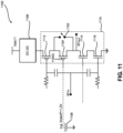
- the bypass switch 1102 may be turned on forming a short across the cascode PFET 1104, which removes the cascode PFET 1104 from a FET stack 1110.
- PFET 1112 and NFETs 1114, 1116 remain active in the FET stack 1110, promoting linear operation.
- the PFET 1104 when the supply voltage is low, the PFET 1104 is turned into an ON switch (equivalent with a short). To do so, the gate terminal 1104G of the PFET 1104 is biased such that the PFET 1104 operates in a triode region and acts like a short. In some cases, such dynamic bias voltage needed to turn the PFET 1104 into an ON switch may need to go negative (i.e., below a ground potential). Generating a negative bias for this situation may require additional complexity such as providing, for example, a charge pump.
- a power amplifier stage 1200 includes a cascoded FET stack 1204.
- the cascoded FET stack 1204 includes PFETs 1206(1), 1206(2) and NFETs 1208(1), 1208(2).
- the FET stack 1204 may couple to a supply 1210 and receive an input signal (RFin) from an input node 1212 while providing an output signal (RFout) at an output node 1214.
- the input node 1212 may be coupled to gates 1206(1)G, 1208(1)G of the FETs 1206(1), 1208(1) through capacitors 1216, 1218, respectively.
- Bias signals may be provided from a bias circuit (not shown) to the gates 1206(1)G, 1208(1)G through respective resistors 1230, 1232. Additional bias signals may be provided from the bias circuit to gates 1206(2)G, 1208(2)G.
- a bypass switch may be implemented as an NFET 1234 coupled to a source 1236. When the supply 1210 drops below the value of the source 1236, the NFET 1234 shorts and the PFET 1206(2) is bypassed. Otherwise, the NFET 1234 is open and the PFET 1206(2) remains as a cascoded FET for the FET stack 1204.
- This concept of removing the cascoded PFETs may be extended to larger cascode stacks as illustrated in Figure 13 , where multiple NFETs 1300(1)-1300(2) may be used to bypass cascode PFETs 1302(1)-1302(2) in a FET stack 1304 of a power amplifier stage 1306.
- the stack of NFETs 1300(1)-1300(2) may be useful in withstanding large signals levels when the switch is in an OFF state (at larger supply voltage values).
- the 5G signals can have modulated bandwidths from several tens of megahertz up through several hundreds of megahertz. For example, if the RF signal modulation bandwidth is 100 MHz, the bandwidth of the supply circuit may need to be around 500 MHz, which is difficult using existing techniques. Most supplies are formed from regulators or DC-DC converters and are likely to have insufficient bandwidth. When a regulator 1400 with an insufficient bandwidth supplies a power amplifier 1402 within a power amplifier stage 1404 as illustrated in Figure 14 , the supply may assume an asymmetric wave form 1406, which leads to distortion at an output 1408 of the power amplifier stage 1404. This distortion can be particularly troubling for complementary amplifiers that have the PFET side of the amplifier exposed to the supply voltage variation. An asymmetry in the supply signal variation will thus result in an asymmetry and distortion in the signal path.
- a supply 1502 which may be a regulator or a DC-DC converter, may have insufficient bandwidth in its provision of a common-mode supply to a power amplifier stack 1504, when compared with a generalized multiplier (e.g., 3 to 6) of the RF signal modulation bandwidth.
- a current sensor 1506 may be associated with the supply line 1508. The sensed current may be conditioned through a processing circuit 1510, which may be, for example, an envelope processing circuit. The output of the processing circuit 1510 may be injected into the supply 1502 or onto the supply line 1508 to form a fast feed forward path. This feedback allows the asymmetries in the supply to be reduced or eliminated such that a small amplitude symmetric supply waveform 1512 is provided to the power amplifier stack 1504.
- a filter 1602 may be added to the feedback loop.
- the power amplifier stage 1600 is similar to the power amplifier stage 1500 of Figure 15 .
- the power amplifier stage 1600 allows for a relatively low bandwidth supply circuit (e.g., regulator) to provide the lower frequency component of the power amplifier supply current, while the higher frequency component of the supply current is provided by the fast feed-forward loop. As such, the limited bandwidth of the supply circuit does not result in distortions in the power amplifier.
- a relatively low bandwidth supply circuit e.g., regulator
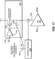
- the supply 1502 may include an input node 1700 that receives a reference voltage (Vref).
- the reference voltage may be amplified by an amplifier 1702.
- An output 1704 from the amplifier 1702 is provided to a capacitor 1706 and a PFET 1708.
- the filter 1602 may be a capacitor, and the processing circuit 1510 may be omitted.
- Current from the current sensor 1506 may be provided to the capacitor 1706 of the supply line 1508.
- the power amplifier stage 1800 may include a FET stack 1802 that is coupled to the supply 1502.
- the FET stack 1802 may include a PFET 1804 and an NFET 1806 and optional cascode FETs 1808, 1810.
- the input node 1212 may be coupled to a capacitor 1812 and current sensor 1814, which may be an NFET, which effectively acts like a current mirror that mirrors the current in the NFET 1806 with NFET 1816.
- the high frequency current component of the feed-forward path may be injected directly at the power amplifier supply line, for example, using an AC coupling capacitance that isolates the DC level from the power amplifier supply and the DC level from the feed-forward path.
- the high frequency current component of the feed-forward path may be injected at the power amplifier supply line using a capacitor already present in the circuit, such as the compensation capacitance of the supply circuit.
- a capacitor already present in the circuit such as the compensation capacitance of the supply circuit.
- One such example is a PFET 1708 output regulator 1502 that has a Miller compensation capacitance 1706 connected from the gate to the drain of the regulator output PFET device as shown in Figure 18 .
- a computer readable medium may include non-transitory type media such as physical storage media including storage discs and solid state devices.
- a computer readable medium may also or alternatively include transient media such as carrier signals and transmission media.
- a computer-readable storage medium is defined herein as a non-transitory memory device.
- a memory device includes memory space within a single physical storage device or memory space spread across multiple physical storage devices.
- CMOS complementary metal oxide semiconductor
- NFETs cascoded n-type field effect transistors
- PFETs cascoded p-type FETs
- a further feedback network may be associated with the supply voltage to assist in providing a symmetrical supply signal. The symmetrical supply signal allows for supply variations without introducing distortion for the power amplifier stage.
Landscapes
- Engineering & Computer Science (AREA)
- Power Engineering (AREA)
- Computer Networks & Wireless Communication (AREA)
- Signal Processing (AREA)
- Amplifiers (AREA)
Abstract
Description
- The technology of the disclosure relates generally to power amplifiers and more particularly, to complementary metal oxide semiconductor (CMOS) power amplifiers with a feedback loop.
- Computing devices abound in modern society, and more particularly, mobile communication devices have become increasingly common. The prevalence of these mobile communication devices is driven in part by the many functions that are now enabled on such devices. Increased processing capabilities in such devices means that mobile communication devices have evolved from pure communication tools into sophisticated mobile entertainment centers, thus enabling enhanced user experiences. Almost all mobile communication devices rely on power amplifiers in at least the transmission chains. While there are myriad ways in which power amplifiers may be formed, the advent of the Fifth Generation-New Radio (5G-NR) cellular standard has placed additional pressure on finding efficient power amplifiers that operate linearly at the frequencies of interest for 5G-NR.
- Particular embodiments are set out in the independent claims. Various optional examples are set out in the dependent claims. Aspects disclosed in the detailed description include a power amplifier using multi-path common-mode feedback loops for radio frequency linearization. In particular, a complementary metal oxide semiconductor (CMOS) power amplifier containing cascoded n-type field effect transistors (FETs) (NFETs) and cascoded p-type FETs (PFETs) may have a common-mode feedback network and provides bias voltages that are dynamically varying with the signal power to keep the output common-mode fixed around a half-supply level, while the small-signal and large-signal transconductances of the FETs are kept balanced. A further feedback network may be associated with the supply voltage to assist in providing a symmetrical supply signal. The symmetrical supply signal allows for supply variations without introducing distortion for the power amplifier stage. This arrangement provides linear operation over temperature corners, process corners, supply voltage corners, and the like.
- In this regard in one aspect, a power amplifier stage is disclosed. The power amplifier stage comprises an input. The power amplifier stage also comprises an output. The power amplifier stage also comprises at least one amplifying device. The power amplifier stage also comprises a bias circuit. The power amplifier stage also comprises a common-mode feedback loop coupled to the output and the bias circuit. The common-mode feedback loop comprises a voltage sensor configured to sense a common-mode voltage at the output, wherein respective bias signals are based on the sensed common-mode voltage. The power amplifier stage also comprises at least one asymmetric dynamic feedback circuit coupled from the output of the power amplifier stage to at least one bias terminal of the power amplifier stage.
- In another aspect, a power amplifier stage is disclosed. The power amplifier stage comprises an input. The power amplifier stage also comprises an output. The power amplifier stage also comprises a common-mode supply input. The power amplifier stage also comprises a supply circuit that has insufficient bandwidth for a given radio frequency (RF) signal modulation bandwidth. The power amplifier stage also comprises a supply current sensing circuit that extracts an envelope component of a supply current. The power amplifier stage also comprises a fast feed-forward branch that bypasses the supply circuit with the insufficient bandwidth, by providing a high-frequency supply current for the power amplifier stage.
- In another aspect, a power amplifier stage is disclosed. The power amplifier stage comprises an input. The power amplifier stage also comprises an output. The power amplifier stage also comprises a common-mode supply circuit with insufficient bandwidth. The power amplifier stage also comprises a bias circuit coupled to a first gate and coupled to a second gate. The bias circuit is configured to bias dynamically the first gate and the second gate with respective bias signals. The power amplifier stage also comprises a bias feedback loop coupled to the output and the bias circuit. The bias feedback loop comprises a voltage sensor configured to sense voltage at the output, wherein the respective bias signals are based on the sensed voltage. The power amplifier stage also comprises a common-mode supply feed-forward path comprising a current sensor configured to sense a high-frequency envelope current of the power amplifier stage and inject a properly-scaled current back into a power amplifier supply line to bypass the common-mode supply circuit with the insufficient bandwidth.
- In another aspect, a power amplifier stage is disclosed. The power amplifier stage comprises an input. The power amplifier stage also comprises an output. The power amplifier stage also comprises a first NFET comprising a first gate. The first NFET is coupled to the input and the output. The power amplifier stage also comprises a first PFET comprising a second gate. The first PFET is coupled to the input and the output. The power amplifier stage also comprises a bias circuit coupled to the first gate and coupled to the second gate. The bias circuit is configured to bias dynamically the first gate and the second gate with respective bias signals. The power amplifier stage also comprises a feedback loop coupled to the output and the bias circuit. The feedback loop comprises a voltage sensor configured to sense voltage at the output, wherein the respective bias signals are based on the sensed voltage.
- In another aspect, a power amplifier stage is disclosed. The power amplifier stage comprises an input. The power amplifier stage also comprises an output. The power amplifier stage also comprises a common-mode supply input. The power amplifier stage also comprises a first NFET comprising a first gate. The first NFET is coupled to the input and the output. The power amplifier stage also comprises a first PFET comprising a second gate. The first PFET is coupled to the input and the output and the common-mode supply input. The power amplifier stage also comprises a feedback loop comprising a current sensor configured to sense current for the first PFET and adjust a signal from the common-mode supply input based on the sensed current.
- In another aspect, a power amplifier stage is disclosed. The power amplifier stage comprises an input. The power amplifier stage also comprises an output. The power amplifier stage also comprises a common-mode supply input. The power amplifier stage also comprises a first NFET comprising a first gate. The first NFET is coupled to the input and the output. The power amplifier stage also comprises a first PFET comprising a second gate. The first PFET is coupled to the input and the output. The power amplifier stage also comprises a bias circuit coupled to the first gate and coupled to the second gate. The bias circuit is configured to bias dynamically the first gate and the second gate with respective bias signals. The power amplifier stage also comprises a bias feedback loop coupled to the output and the bias circuit. The bias feedback loop comprises a voltage sensor configured to sense voltage at the output, wherein the respective bias signals are based on the sensed voltage. The power amplifier stage also comprises a common-mode supply feedback loop comprising a current sensor configured to sense current for the first PFET and adjust a signal from the common-mode supply input based on the sensed current.
-
-
Figure 1 is a block diagram of a power amplifier stage with a common-mode bias input and a common-mode supply input; -
Figure 2 is a block diagram of a power amplifier stage having a common-mode supply feedback loop to assist in providing linearity for the power amplifier stage; -
Figure 3 is a block diagram of a power amplifier stage having a common-mode bias feedback loop to assist in providing linearity for the power amplifier stage; -
Figure 4 is a block diagram of a power amplifier stage having two feedback loops, one for the common-mode supply and one for the common-mode bias circuit to assist in providing linearity for the power amplifier stage; -
Figures 5A and5B illustrate single-ended and differential-ended power amplifier structures that may implement the feedback loops of the present disclosure to assist in linearization; -
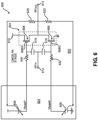
Figure 6 is a circuit diagram showing further details of the common-mode bias feedback loop for a non-cascoded complementary metal oxide semiconductor (CMOS) power amplifier stage; -
Figure 7 is a circuit diagram showing further details of the common-mode bias feedback loop for a cascoded CMOS power amplifier stage; -
Figure 8 is a circuit diagram showing further details of the common-mode bias feedback loop for a cascoded CMOS power amplifier stage where bias for the cascoded amplifiers is also dynamically adjusted by the feedback loop; -
Figure 9A is a circuit diagram showing further details of the common-mode bias feedback loop for the cascoded CMOS power amplifier stage ofFigure 8 with additional compensation for drains of the cascoded amplifiers; -
Figure 9B is a circuit diagram similar to the CMOS power amplifier stage ofFigure 9A , but with generic asymmetric voltage dividers for the dynamic common-mode biasing; -
Figure 10 is a circuit diagram of a CMOS power amplifier stage that may have a common-mode bias feedback loop, but also suffers performance problems when a voltage supply dips below a threshold, crushing a cascoded amplifier; -
Figure 11 is a circuit diagram of a CMOS power amplifier stage that may have a common-mode bias feedback loop with a bypass switch to prevent crushing the cascoded amplifier; -
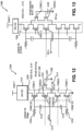
Figure 12 is a circuit diagram showing one possible implementation of the bypass switch ofFigure 11 ; -
Figure 13 is a circuit diagram showing how the bypass switch ofFigure 12 may be expanded to a larger cascode stack; -
Figure 14 is a block diagram of a power amplifier stage having a voltage supply that lacks sufficient bandwidth for the signals being amplified by the power amplifier stage; -
Figure 15 is a block diagram of a power amplifier stage with a common-mode supply feedback loop that senses current from the voltage supply and modulates the supply signal to provide a symmetric supply waveform; -
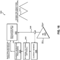
Figure 16 is a block diagram of a power amplifier stage similar to that ofFigure 15 , but with optional signal filtering; -
Figure 17 is a mixed block and circuit diagram showing details of how the feedback signal ofFigures 15 and16 may be used to modulate the supply signal; and -
Figure 18 is a circuit diagram showing an alternate way to sense current to assist in forming the common-mode supply feedback loop. - The embodiments set forth below represent the necessary information to enable those skilled in the art to practice the embodiments and illustrate the best mode of practicing the embodiments. Upon reading the following description in light of the accompanying drawing figures, those skilled in the art will understand the concepts of the disclosure and will recognize applications of these concepts not particularly addressed herein. It should be understood that these concepts and applications fall within the scope of the disclosure and the accompanying claims.
- It will be understood that, although the terms first, second, etc. may be used herein to describe various elements, these elements should not be limited by these terms. These terms are only used to distinguish one element from another. For example, a first element could be termed a second element, and, similarly, a second element could be termed a first element, without departing from the scope of the present disclosure. As used herein, the term "and/or" includes any and all combinations of one or more of the associated listed items.
- It will be understood that when an element such as a layer, region, or substrate is referred to as being "on" or extending "onto" another element, it can be directly on or extend directly onto the other element or intervening elements may also be present. In contrast, when an element is referred to as being "directly on" or extending "directly onto" another element, there are no intervening elements present. Likewise, it will be understood that when an element such as a layer, region, or substrate is referred to as being "over" or extending "over" another element, it can be directly over or extend directly over the other element or intervening elements may also be present. In contrast, when an element is referred to as being "directly over" or extending "directly over" another element, there are no intervening elements present. It will also be understood that when an element is referred to as being "connected" or "coupled" to another element, it can be directly connected or coupled to the other element or intervening elements may be present. In contrast, when an element is referred to as being "directly connected" or "directly coupled" to another element, there are no intervening elements present.
- Relative terms such as "below" or "above" or "upper" or "lower" or "horizontal" or "vertical" may be used herein to describe a relationship of one element, layer, or region to another element, layer, or region as illustrated in the Figures. It will be understood that these terms and those discussed above are intended to encompass different orientations of the device in addition to the orientation depicted in the Figures.
- The terminology used herein is for the purpose of describing particular embodiments only and is not intended to be limiting of the disclosure. As used herein, the singular forms "a," "an," and "the" are intended to include the plural forms as well, unless the context clearly indicates otherwise. It will be further understood that the terms "comprises," "comprising," "includes," and/or "including" when used herein specify the presence of stated features, integers, steps, operations, elements, and/or components, but do not preclude the presence or addition of one or more other features, integers, steps, operations, elements, components, and/or groups thereof.
- Unless otherwise defined, all terms (including technical and scientific terms) used herein have the same meaning as commonly understood by one of ordinary skill in the art to which this disclosure belongs. It will be further understood that terms used herein should be interpreted as having a meaning that is consistent with their meaning in the context of this specification and the relevant art and will not be interpreted in an idealized or overly formal sense unless expressly so defined herein.
- Aspects disclosed in the detailed description include a power amplifier using multi-path common-mode feedback loops for radio frequency linearization. In particular, a complementary metal oxide semiconductor (CMOS) power amplifier containing cascoded n-type field effect transistors (FETs) (NFETs) and cascoded p-type FETs (PFETs) may have a common-mode feedback network and provides bias voltages that are dynamically varying with the signal power to keep the output common-mode fixed around a half-supply level, while the small-signal and large-signal transconductances of the FETs are kept balanced. A further feedback network may be associated with the supply voltage to assist in providing a symmetrical supply signal. The symmetrical supply signal allows for supply variations without introducing distortion for the power amplifier stage. This arrangement provides linear operation over temperature corners, process corners, supply voltage corners, and the like.
- Before addressing aspects of the present disclosure, an explanation of the challenges facing a power amplifier operating across a wide range of frequencies is provided. In the past, a power amplifier might use a hybrid approach, where the power amplifier proper might be implemented in bipolar technologies using a material such as Gallium Arsenide (GaAs). The power amplifier might be controlled by a CMOS stage that has a driver amplifier, biasing circuitry, and the like. While effective at providing an acceptable cost-performance compromise while allowing tunability through, for example, a matching network and/or load line, such systems are complex and have a relatively long design cycle. Moving to a power amplifier that implements both the power amplifier as well as the control circuit in CMOS technology generally relies on nanometer CMOS processes. Such devices, and particularly the FETs of such devices, can tolerate maximum voltages much lower than typical battery voltage levels. Accordingly, such devices may rely on cascode structures, where FETs are stacked relative to one another.
- Existing techniques to set a common-mode output voltage level for CMOS power amplifiers involve using a direct bias of the output node from a voltage generator or using a resistor feedback that also sets the common-mode output voltage level. However, such techniques do not offer any way to control the linearity of the stage. Specifically, the FETs in a CMOS device may have a transconductance which varies from small signal to large signal. Keeping a good linearity of the power amplifier stage requires having the NFETs and PFETs maintain balanced transconductances both at small signal and large signal levels. This balance is not readily accessible without having a dedicated circuit for such task. When the common-mode supply moves down, it reduces headroom available for the NFET, while when the common-mode supply moves up, it reduces headroom available for the PFET. Both actions result in distortions at large signal levels. If the transconductance is matched for large signals, there will be different transconductances at the small signal level, resulting in distortions at moderate signal levels. This distortion negatively impacts performance.
-
Figure 1 illustrates a block diagram of apower amplifier stage 100 that has two common-mode inputs, which impact linearity. Specifically, there is avoltage source 102, e.g., VBATT, which is a common-mode supply for apower amplifier 104. Thepower amplifier 104 also receives a common-mode bias signal from abias circuit 106. Further, thepower amplifier 104 receives an RF input signal (RFin) and provides an RF output signal (RFout). Maintaining linearity while using these two common-mode inputs provides opportunities for improvement. - Aspects of the present disclosure provide two complimentary ways which singly or together help provide linearity for the power amplifier stage. In particular, aspects of a first of the complimentary ways of the present disclosure provide bias voltages that are dynamically varying with the signal power to keep the output common-mode fixed around a half-supply level, while the small-signal and large-signal transconductances of the FETs are kept balanced. This arrangement provides linear operation over temperature corners, process corners, supply voltage corners, and the like.
- In this regard,
Figure 2 illustrates apower amplifier stage 200 that has a common-mode supply correction orfeedback loop 202 that modifies asupply voltage signal 204 provided to apower amplifier 206 from a voltage supply 208 (e.g., VBATT). A common-mode bias circuit 210 is not modified in thepower amplifier stage 200 and is substantially similar to thebias circuit 106 ofFigure 1 . The common-modesupply feedback loop 202 includes acurrent sensing circuit 212 and anenvelope filter circuit 214. More details are provided below with reference toFigures 15-18 . It should be appreciated that the current sensing is done indirectly as indicated by the loop feeding into thecurrent sensing circuit 212. - In contrast,
Figure 3 illustrates apower amplifier stage 300 that has a common-mode bias correction orfeedback loop 302 that modifies a common-mode bias signal from abias circuit 304 to apower amplifier 306. Thepower amplifier 306 receives a common-mode supply voltage signal from avoltage supply 308. The common-modebias feedback loop 302 includes a common-mode voltage sensor 310 that measures the common-mode voltage of the output port RFout. The common-modebias feedback loop 302 also includes an asymmetric dynamic signal to help balance the transconductances. - While the
feedback loops power amplifier stage 400 illustrated inFigure 4 includes both the common-modesupply feedback loop 202 and the common-modebias feedback loop 302 with apower amplifier 402. - Before addressing details of the present disclosure, it should be appreciated that the concepts of the present disclosure have wide application. While most of the examples provided below focus on single-ended power amplifier stages, the present disclosure is not so limited. Thus, while
Figure 5A illustrates explicitly a single-endedpower amplifier stage 500,Figure 5B illustrates a differentialpower amplifier stage 550, and it should be appreciated that the concepts of the present disclosure may be extended to quadrature power amplifier stages (not shown) and Doherty, barely Doherty, out-phasing, and the like (also not shown) without departing from the present disclosure. - Returning to
Figure 5A , the single-endedpower amplifier stage 500 includes aCMOS power amplifier 502 havingNFETs 504 andPFETs 506. The common-modesupply feedback loop 202 is provided above the PFETs 506 (i.e., betweenVBATT 508 and a PFET 506). Likewise, the common-modebias feedback loop 302 works with bias circuit 304' to provide multiple bias signals to theNFETs 504 and thePFETs 506. Again, it should be appreciated that the current sensing of the common-modesupply feedback loop 202 is indirect. - In
Figure 5B , the differentialpower amplifier stage 550 includes two CMOS power amplifier stacks 552(1), 552(1) havingNFETs PFETs supply feedback loop 202 is provided above thePFETs bias feedback loop 302 works with abias circuit 304" to provide multiple bias signals to theNFETs PFETs supply feedback loop 202 is indirect. - A discussion of the common-mode
bias feedback loop 302 is provided with reference toFigures 6-9 . In particular, the common-modebias feedback loop 302 may be implemented in a simple CMOSpower amplifier stage 600 asloop 602. Thepower amplifier stage 600 may include aFET stack 604 including aPFET 606 and anNFET 608. TheFET stack 604 may couple to asupply 610 and receive an input signal (RFin) from aninput node 612 while providing an output signal (RFout) at anoutput node 614. Theinput node 612 may be coupled togates 606G, 608G of theFETs capacitors output node 614 may be coupled toresistors bias circuit 624. Thebias circuit 624 may include a first variable source 626 and a secondvariable source 628 that are controlled based on the signal from theoutput node 614. Thevariable sources 626, 628 provide bias signals to thegates 606G, 608G, respectively, throughrespective resistors gates 606G, 608G, the common-mode voltage at theoutput node 614 may be kept at about half the supply voltage from thesupply 610. - While effective, the CMOS
power amplifier stage 600 is limited in that the total swing is limited by thesingle NFET 608 andsingle PFET 606. More commonly, a CMOS power amplifier stage will have cascoded FETs as shown inpower amplifier stage 700 illustrated inFigure 7 . Thepower amplifier stage 700 includes aloop 702, analogous to theloop 602 ofFigure 6 , but accommodating acascoded FET stack 704. Thecascoded FET stack 704 includes PFETs 706(1), 706(2) and NFETs 708(1), 708(2). TheFET stack 704 may couple to asupply 710 and receive an input signal (RFin) from aninput node 712 while providing an output signal (RFout) at anoutput node 714. Theinput node 712 may be coupled togates 706G, 708G of the FETs 706(1), 708(1) through capacitors 716, 718, respectively. Theoutput node 714 may be coupled toresistors bias circuit 724. Thebias circuit 724 may include a first variable source 726 and a secondvariable source 728 that are controlled based on the signal from theoutput node 714. Thevariable sources 726, 728 provide bias signals to thegates 706G, 708G, respectively, throughrespective resistors gates 706G, 708G, the signal at theoutput node 714 may be kept at about half the supply voltage from thesupply 710. - Controlling the bias of the FETs 706(1), 708(1) may be insufficient to hold the output node at about half the supply. Accordingly, it may be appropriate also to bias the cascoded devices in the amplifier stack as illustrated by
power amplifier stage 800 inFigure 8 . Thepower amplifier stage 800 includes aloop 802, analogous to theloop 602 ofFigure 6 , but accommodating acascoded FET stack 804. Thecascoded FET stack 804 includes PFETs 806(1), 806(2) and NFETs 808(1), 808(2). TheFET stack 804 may couple to asupply 810 and receive an input signal (RFin) from aninput node 812 while providing an output signal (RFout) at anoutput node 814. Theinput node 812 may be coupled to gates 806(1)G, 808(1)G of the FETs 806(1), 808(1) throughcapacitors output node 814 may be coupled toresistors bias circuit 824. Thebias circuit 824 may include a firstvariable source 826 and a secondvariable source 828 that are controlled based on the signal from theoutput node 814. Thevariable sources respective resistors variable sources resistors output node 814 may be kept at about half the supply voltage from thesupply 810. Note that while only one cascoded FET is shown on each half of thestack 804, the concept may be extended to larger cascoded stacks without departing from the present disclosure. - Sometimes it may not even be sufficient to bias the cascoded devices in the amplifier stack. Accordingly, an additional measure may be to control the drains of the cascoded devices as illustrated by
power amplifier stage 900 inFigure 9A . Thepower amplifier stage 900 includesloop 902, analogous to theloop 602 ofFigure 6 , but accommodating acascoded FET stack 904. Thecascoded FET stack 904 includes PFETs 906(1), 906(2) and NFETs 908(1), 908(2). TheFET stack 904 may couple to asupply 910 and receive an input signal (RFin) from aninput node 912 while providing an output signal (RFout) at anoutput node 914. Theinput node 912 may be coupled to gates 906(1)G, 908(1)G of the FETs 906(1), 908(1) throughcapacitors output node 914 may be coupled toresistors bias circuit 924. Thebias circuit 924 may include a firstvariable source 926 and a secondvariable source 928 that are controlled based on the signal from theoutput node 914. Thevariable sources respective resistors variable sources resistors capacitors varactors output node 914 may be kept at about half the supply voltage from thesupply 910. Further, the use of thevaractors output node 914 at about half the supply voltage from thesupply 910. -
Figure 9B shows apower amplifier stage 950, which is substantially similar to thepower amplifier stage 900, and common elements maintain common numbering. However, in place of thecapacitors varactors 942, 944 a more generalized asymmetric outputvoltage divider circuit - There may be occasions when the nature of the cascode stack works against linear operation of the power amplifier stage. For example, if a
cascoded PFET 1000 in apower amplifier stage 1002 illustrated inFigure 10 is biased to some point (e.g., 1.2 volts (V)), then thesupply 1004 needs to be somewhere above that point (e.g., + 0.3 V) to keep thePFET 1006 turned on. Thus, if thesupply 1004 dips below a certain threshold (e.g., in this case 1.5 V), the PFET portion of theFET stack 1008 will collapse and turn off. Turning off the PFET portion of theFET stack 1008 negatively impacts the ability of thepower amplifier stage 1002 to operate linearly. - Aspects of the present disclosure provide a solution to prevent collapse of the PFET portion of a
power amplifier stage 1100 as shown inFigure 11 . Specifically, abypass switch 1102 is placed around acascode PFET 1104. When thesupply 1106 drops below a predetermined threshold corresponding approximately to thebias source 1108 of thecascode PFET 1104, thebypass switch 1102 may be turned on forming a short across thecascode PFET 1104, which removes thecascode PFET 1104 from aFET stack 1110.PFET 1112 andNFETs 1114, 1116 remain active in theFET stack 1110, promoting linear operation. - In an alternate aspect (not illustrated), when the supply voltage is low, the
PFET 1104 is turned into an ON switch (equivalent with a short). To do so, thegate terminal 1104G of thePFET 1104 is biased such that thePFET 1104 operates in a triode region and acts like a short. In some cases, such dynamic bias voltage needed to turn thePFET 1104 into an ON switch may need to go negative (i.e., below a ground potential). Generating a negative bias for this situation may require additional complexity such as providing, for example, a charge pump. -
Figures 12 and 13 show possible implementations of thebypass switch 1102. Specifically, inFigure 12 , apower amplifier stage 1200 includes acascoded FET stack 1204. Thecascoded FET stack 1204 includes PFETs 1206(1), 1206(2) and NFETs 1208(1), 1208(2). TheFET stack 1204 may couple to asupply 1210 and receive an input signal (RFin) from aninput node 1212 while providing an output signal (RFout) at anoutput node 1214. Theinput node 1212 may be coupled to gates 1206(1)G, 1208(1)G of the FETs 1206(1), 1208(1) throughcapacitors respective resistors NFET 1234 coupled to asource 1236. When thesupply 1210 drops below the value of thesource 1236, theNFET 1234 shorts and the PFET 1206(2) is bypassed. Otherwise, theNFET 1234 is open and the PFET 1206(2) remains as a cascoded FET for theFET stack 1204. - This concept of removing the cascoded PFETs may be extended to larger cascode stacks as illustrated in
Figure 13 , where multiple NFETs 1300(1)-1300(2) may be used to bypass cascode PFETs 1302(1)-1302(2) in aFET stack 1304 of apower amplifier stage 1306. The stack of NFETs 1300(1)-1300(2) may be useful in withstanding large signals levels when the switch is in an OFF state (at larger supply voltage values). - As noted above, there is another common-source input for many amplifier stages, and that is a common-mode supply source. Normally, such supplies need to have a bandwidth larger than a modulation bandwidth supported by the power amplifier stage. For lower modulation bandwidths of the RF signal (e.g., 200 kHz, 4 MHz, etc.), this constraint can be supported with supply circuits having existing techniques. The bandwidth of the supply circuits may need to be three to six (3-6) times larger than the RF signal modulation bandwidth, which may go up to around 24 MHz. Existing techniques support such bandwidths. However, the advent of 5G-NR with its operational ranges in the gigahertz has correspondingly increased the modulation bandwidth to increase the supported data rates. Routinely, the 5G signals can have modulated bandwidths from several tens of megahertz up through several hundreds of megahertz. For example, if the RF signal modulation bandwidth is 100 MHz, the bandwidth of the supply circuit may need to be around 500 MHz, which is difficult using existing techniques. Most supplies are formed from regulators or DC-DC converters and are likely to have insufficient bandwidth. When a regulator 1400 with an insufficient bandwidth supplies a
power amplifier 1402 within apower amplifier stage 1404 as illustrated inFigure 14 , the supply may assume anasymmetric wave form 1406, which leads to distortion at anoutput 1408 of thepower amplifier stage 1404. This distortion can be particularly troubling for complementary amplifiers that have the PFET side of the amplifier exposed to the supply voltage variation. An asymmetry in the supply signal variation will thus result in an asymmetry and distortion in the signal path. - A solution to this problem is to use the common-mode
supply feedback loop 202 described above. More detail is provided bypower amplifier stage 1500 with reference toFigure 15 . Specifically, asupply 1502, which may be a regulator or a DC-DC converter, may have insufficient bandwidth in its provision of a common-mode supply to apower amplifier stack 1504, when compared with a generalized multiplier (e.g., 3 to 6) of the RF signal modulation bandwidth. Acurrent sensor 1506 may be associated with thesupply line 1508. The sensed current may be conditioned through aprocessing circuit 1510, which may be, for example, an envelope processing circuit. The output of theprocessing circuit 1510 may be injected into thesupply 1502 or onto thesupply line 1508 to form a fast feed forward path. This feedback allows the asymmetries in the supply to be reduced or eliminated such that a small amplitudesymmetric supply waveform 1512 is provided to thepower amplifier stack 1504. - As an additional improvement shown by
power amplifier stage 1600 inFigure 16 , afilter 1602 may be added to the feedback loop. In other respects, thepower amplifier stage 1600 is similar to thepower amplifier stage 1500 ofFigure 15 . - The
power amplifier stage 1600 allows for a relatively low bandwidth supply circuit (e.g., regulator) to provide the lower frequency component of the power amplifier supply current, while the higher frequency component of the supply current is provided by the fast feed-forward loop. As such, the limited bandwidth of the supply circuit does not result in distortions in the power amplifier. - More details for the injection process are shown in
Figure 17 , where thesupply 1502 may include aninput node 1700 that receives a reference voltage (Vref). The reference voltage may be amplified by anamplifier 1702. Anoutput 1704 from theamplifier 1702 is provided to acapacitor 1706 and aPFET 1708. Thefilter 1602 may be a capacitor, and theprocessing circuit 1510 may be omitted. Current from thecurrent sensor 1506 may be provided to thecapacitor 1706 of thesupply line 1508. - Instead of sensing current directly on the
supply line 1508, current may be sensed indirectly as shown bypower amplifier stage 1800 inFigure 18 . Thepower amplifier stage 1800 may include aFET stack 1802 that is coupled to thesupply 1502. TheFET stack 1802 may include aPFET 1804 and anNFET 1806 andoptional cascode FETs input node 1212 may be coupled to acapacitor 1812 andcurrent sensor 1814, which may be an NFET, which effectively acts like a current mirror that mirrors the current in theNFET 1806 withNFET 1816. - The high frequency current component of the feed-forward path may be injected directly at the power amplifier supply line, for example, using an AC coupling capacitance that isolates the DC level from the power amplifier supply and the DC level from the feed-forward path.
- In an alternate aspect, the high frequency current component of the feed-forward path may be injected at the power amplifier supply line using a capacitor already present in the circuit, such as the compensation capacitance of the supply circuit. One such example is a
PFET 1708output regulator 1502 that has aMiller compensation capacitance 1706 connected from the gate to the drain of the regulator output PFET device as shown inFigure 18 . - A computer readable medium may include non-transitory type media such as physical storage media including storage discs and solid state devices. A computer readable medium may also or alternatively include transient media such as carrier signals and transmission media. A computer-readable storage medium is defined herein as a non-transitory memory device. A memory device includes memory space within a single physical storage device or memory space spread across multiple physical storage devices.
- The previous description of the disclosure is provided to enable any person skilled in the art to make or use the disclosure. Various modifications to the disclosure will be readily apparent to those skilled in the art, and the generic principles defined herein may be applied to other variations. Thus, the disclosure is not intended to be limited to the examples and designs described herein, but is to be accorded the widest scope consistent with the principles and novel features disclosed herein.
- Thus, from one perspective, there has now been described a power amplifier using multi-path common-mode feedback loops for radio frequency linearization is disclosed. In one aspect, a complementary metal oxide semiconductor (CMOS) power amplifier containing cascoded n-type field effect transistors (NFETs) and cascoded p-type FETs (PFETs) may have a common-mode feedback network and provides bias voltages that are dynamically varying with the signal power to keep the output common-mode fixed around a half-supply level, while the small-signal and large-signal transconductances of the FETs are kept balanced. A further feedback network may be associated with the supply voltage to assist in providing a symmetrical supply signal. The symmetrical supply signal allows for supply variations without introducing distortion for the power amplifier stage.
- Further examples of feature combinations taught by the present disclosure are set out in the following numbered clauses:
- 1. A power amplifier stage comprising:
- an input;
- an output;
- at least one amplifying device;
- a bias circuit;
- a common-mode feedback loop coupled to the output and the bias circuit, the common-mode feedback loop comprising a voltage sensor configured to sense a common-mode voltage at the output, wherein respective bias signals are based on the sensed common-mode voltage; and
- at least one asymmetric dynamic feedback circuit coupled from the output of the power amplifier stage to at least one bias terminal of the power amplifier stage.
- 2. The power amplifier stage of
clause 1, wherein the at least one amplifying device comprises:- a first n-type field effect transistor (FET) (NFET) comprising a first gate, the first NFET coupled to the input and the output;
- a first p-type FET (PFET) comprising a second gate, the first PFET coupled to the input and the output; and
- the bias circuit coupled to the first gate and coupled to the second gate, the bias circuit configured to bias dynamically the first gate and the second gate with the respective bias signals.
- 3. The power amplifier stage of
clause 2, further comprising:- a second NFET cascoded relative to the first NFET; and
- a second PFET cascoded relative to the first PFET.
- 4. The power amplifier stage of clause 3, wherein the second NFET comprises a third gate and the second PFET comprises a fourth gate; and
wherein the bias circuit is coupled to the third gate and the fourth gate. - 5. The power amplifier stage of any preceding clause, further comprising a first asymmetric capacitor divider and a second asymmetric capacitor divider coupled from the output to a P-side of an N-side cascode device gate.
- 6. The power amplifier stage of clause 3, further comprising a bypass switch configured to bypass the second PFET.
- 7. The power amplifier stage of clause 6, wherein the bypass switch comprises a third NFET, and wherein the third NFET is configured to short circuit the second PFET when a voltage supply drops below a threshold.
- 8. A power amplifier stage comprising:
- an input;
- an output;
- a common-mode supply input;
- a supply circuit that has insufficient bandwidth for a given radio frequency (RF) signal modulation bandwidth;
- a supply current sensing circuit that extracts an envelope component of a supply current; and
- a fast feed-forward branch that bypasses the supply circuit with the insufficient bandwidth, by providing a high-frequency supply current for the power amplifier stage.
- 9. The power amplifier stage of clause 8, further comprising:
- a first n-type field effect transistor (FET) (NFET) comprising a first gate, the first NFET coupled to the input and the output;
- a first p-type FET (PFET) comprising a second gate, the first PFET coupled to the input and the output and the common-mode supply input; and
- a feed-forward path comprising a current sensor configured to sense current for the first PFET and adjust a signal from the common-mode supply input based on the sensed current.
- 10. The power amplifier stage of clause 9, wherein the feed-forward path is configured to shape the signal from the common-mode supply input into a symmetric signal.
- 11. The power amplifier stage of clause 9 or 10, further comprising a second NFET cascoded relative to the first NFET and a second PFET cascoded relative to the first PFET.
- 12. The power amplifier stage of any of clauses 9 to 11, wherein the current sensor comprises a current mirror coupled to the input.
- 13. The power amplifier stage of any of clauses 9 to 12, wherein the feed-forward path further comprises a filter.
- 14. The power amplifier stage of any of clauses 9 to 13, wherein the current sensor is coupled to a source of the first PFET and is configured to sense the current directly.
- 15. The power amplifier stage of any of clauses 9 to 14, wherein the current sensor is coupled to the input and is configured to sense the current indirectly.
- 16. A power amplifier stage comprising:
- an input;
- an output;
- a common-mode supply circuit with insufficient bandwidth;
- a bias circuit coupled to a first gate and coupled to a second gate, the bias circuit configured to bias dynamically the first gate and the second gate with respective bias signals;
- a bias feedback loop coupled to the output and the bias circuit, the bias feedback loop comprising a voltage sensor configured to sense voltage at the output, wherein the respective bias signals are based on the sensed voltage; and
- a common-mode supply feed-forward path comprising a current sensor configured to sense a high-frequency envelope current of the power amplifier stage and inject a properly-scaled current back into a power amplifier supply line to bypass the common-mode supply circuit with the insufficient bandwidth.
- 17. The power amplifier stage of clause 16, further comprising:
- a first n-type field effect transistor (FET) (NFET) comprising a first gate, the first NFET coupled to the input and the output; and
- a first p-type FET (PFET) comprising a second gate, the first PFET coupled to the input and the output.
- 18. The power amplifier stage of clause 17, wherein the first NFET and the first PFET form a complementary amplifier.
- 19. The power amplifier stage of clause 16, comprising one or multiple of the following types: field-effect-transistors (FETs), junction-field-effect-transistors (J-FETs), high-electron-mobility-transistors (HEMTs), bipolar transistors (BT), and heterojunction-bipolar-transistors (HBTs).
- 20. The power amplifier stage of clause 19, wherein only N-type devices are present (NFET, N-J-FET, NPN bipolar transistor).
- 21. A power amplifier stage comprising:
- an input;
- an output;
- a first n-type field effect transistor (FET) (NFET) comprising a first gate, the first NFET coupled to the input and the output;
- a first p-type FET (PFET) comprising a second gate, the first PFET coupled to the input and the output;
- a bias circuit coupled to the first gate and coupled to the second gate, the bias circuit configured to bias dynamically the first gate and the second gate with respective bias signals; and
- a feedback loop coupled to the output and the bias circuit, the feedback loop comprising a voltage sensor configured to sense voltage at the output, wherein the respective bias signals are based on the sensed voltage.
- 22. The power amplifier stage of clause 21, wherein the bias circuit comprises at least one variable source.
- 23. The power amplifier stage of clause 21 or 22, further comprising:
- a second NFET cascoded relative to the first NFET; and
- a second PFET cascoded relative to the first PFET.
- 24. The power amplifier stage of clause 23, wherein the second NFET comprises a third gate and the second PFET comprises a fourth gate; and
wherein the bias circuit is coupled to the third gate and the fourth gate - 25. The power amplifier stage of any of clauses 21 to 24, further comprising a first varactor and a second varactor coupled in parallel to the output.
- 26. The power amplifier stage of any of clauses 23 to 25, further comprising a bypass switch configured to bypass the second PFET.
- 27. The power amplifier stage of clause 26, wherein the bypass switch comprises a third NFET, and wherein the third NFET is configured to short circuit the second PFET when a voltage supply drops below a threshold.
- 28. A power amplifier stage comprising:
- an input;
- an output;
- a common-mode supply input;
- a first n-type field effect transistor (FET) (NFET) comprising a first gate, the first NFET coupled to the input and the output;
- a first p-type FET (PFET) comprising a second gate, the first PFET coupled to the input and the output and the common-mode supply input; and
- a feedback loop comprising a current sensor configured to sense current for the first PFET and adjust a signal from the common-mode supply input based on the sensed current.
- 29. The power amplifier stage of clause 28, wherein the feedback loop is configured to shape the signal from the common-mode supply input into a symmetric signal.
- 30. The power amplifier stage of clause 28 or 29, further comprising a second NFET cascoded relative to the first NFET and a second PFET cascoded relative to the first PFET.
- 31. The power amplifier stage of clause 30, wherein the current sensor comprises a current mirror coupled to the input.
- 32. The power amplifier stage of any of clauses 28 to 31, wherein the feedback loop further comprises a filter.
- 33. The power amplifier stage of any of clauses 28 to 32, wherein the current sensor is coupled to a source of the first PFET and is configured to sense current directly.
- 34. The power amplifier stage of any of clauses 28 to 33, wherein the current sensor is coupled to the input and configured to sense current indirectly.
- 35. A power amplifier stage comprising:
- an input;
- an output;
- a common-mode supply input;
- a first n-type field effect transistor (FET) (NFET) comprising a first gate, the first NFET coupled to the input and the output;
- a first p-type FET (PFET) comprising a second gate, the first PFET coupled to the input and the output;
- a bias circuit coupled to the first gate and coupled to the second gate, the bias circuit configured to bias dynamically the first gate and the second gate with respective bias signals;
- a bias feedback loop coupled to the output and the bias circuit, the bias feedback loop comprising a voltage sensor configured to sense voltage at the output, wherein the respective bias signals are based on the sensed voltage; and
- a common-mode supply feedback loop comprising a current sensor configured to sense current for the first PFET and adjust a signal from the common-mode supply input based on the sensed current.
- 36. The power amplifier stage of clause 35, wherein the first NFET and the first PFET form a complementary amplifier.
Claims (15)
- A power amplifier stage comprising:an input;an output;a first n-type field effect transistor (FET) (NFET) comprising a first gate, the first NFET coupled to the input and the output;a first p-type FET (PFET) comprising a second gate, the first PFET coupled to the input and the output;a bias circuit coupled to the first gate and coupled to the second gate, the bias circuit configured to bias dynamically the first gate and the second gate with respective bias signals; anda feedback loop coupled to the output and the bias circuit, the feedback loop comprising a voltage sensor configured to sense voltage at the output, wherein the respective bias signals are based on the sensed voltage.
- The power amplifier stage of claim 1, wherein the bias circuit comprises at least one variable source.
- The power amplifier stage of claim 1 or 2, further comprising:a second NFET cascoded relative to the first NFET; anda second PFET cascoded relative to the first PFET.
- The power amplifier stage of claim 3, wherein the second NFET comprises a third gate and the second PFET comprises a fourth gate; and
wherein the bias circuit is coupled to the third gate and the fourth gate - The power amplifier stage of any preceding claim, further comprising a first varactor and a second varactor coupled in parallel to the output.
- The power amplifier stage of any of claims 3 to 5, further comprising a bypass switch configured to bypass the second PFET.
- The power amplifier stage of claim 6, wherein the bypass switch comprises a third NFET, and wherein the third NFET is configured to short circuit the second PFET when a voltage supply drops below a threshold.
- A power amplifier stage comprising:an input;an output;a common-mode supply input;a first n-type field effect transistor (FET) (NFET) comprising a first gate, the first NFET coupled to the input and the output;a first p-type FET (PFET) comprising a second gate, the first PFET coupled to the input and the output and the common-mode supply input; anda feedback loop comprising a current sensor configured to sense current for the first PFET and adjust a signal from the common-mode supply input based on the sensed current.
- The power amplifier stage of claim 8, wherein the feedback loop is configured to shape the signal from the common-mode supply input into a symmetric signal.
- The power amplifier stage of claim 8 or 9, further comprising a second NFET cascoded relative to the first NFET and a second PFET cascoded relative to the first PFET.
- The power amplifier stage of claim 10, wherein the current sensor comprises a current mirror coupled to the input.
- The power amplifier stage of any of claims 8 to 11, wherein the feedback loop further comprises a filter.
- The power amplifier stage of any of claims 8 to 12, wherein the current sensor is coupled to a source of the first PFET and is configured to sense current directly.
- The power amplifier stage of any of claims 8 to 13, wherein the current sensor is coupled to the input and configured to sense current indirectly.
- A power amplifier stage comprising:an input;an output;a common-mode supply input;a first n-type field effect transistor (FET) (NFET) comprising a first gate, the first NFET coupled to the input and the output;a first p-type FET (PFET) comprising a second gate, the first PFET coupled to the input and the output;a bias circuit coupled to the first gate and coupled to the second gate, the bias circuit configured to bias dynamically the first gate and the second gate with respective bias signals;a bias feedback loop coupled to the output and the bias circuit, the bias feedback loop comprising a voltage sensor configured to sense voltage at the output, wherein the respective bias signals are based on the sensed voltage; anda common-mode supply feedback loop comprising a current sensor configured to sense current for the first PFET and adjust a signal from the common-mode supply input based on the sensed current,wherein the first NFET and the first PFET optionally form a complementary amplifier.
Applications Claiming Priority (1)
| Application Number | Priority Date | Filing Date | Title |
|---|---|---|---|
| US17/588,799 US12368418B2 (en) | 2022-01-31 | 2022-01-31 | Power amplifier using multi-path common-mode feedback loop |
Publications (2)
| Publication Number | Publication Date |
|---|---|
| EP4231524A2 true EP4231524A2 (en) | 2023-08-23 |
| EP4231524A3 EP4231524A3 (en) | 2023-11-29 |
Family
ID=85150756
Family Applications (1)
| Application Number | Title | Priority Date | Filing Date |
|---|---|---|---|
| EP23154128.5A Pending EP4231524A3 (en) | 2022-01-31 | 2023-01-31 | Power amplifier using multi-path common-mode feedback loop |
Country Status (4)
| Country | Link |
|---|---|
| US (2) | US12368418B2 (en) |
| EP (1) | EP4231524A3 (en) |
| KR (1) | KR20230117527A (en) |
| CN (1) | CN116526993A (en) |
Families Citing this family (2)
| Publication number | Priority date | Publication date | Assignee | Title |
|---|---|---|---|---|
| WO2025207200A1 (en) * | 2024-03-25 | 2025-10-02 | Qorvo Us, Inc. | Current reuse low noise amplifier (lna) |
| DE102024128147A1 (en) * | 2024-09-27 | 2026-04-02 | Valeo Eautomotive Germany Gmbh | Active interference compensation circuit for an electronic device and method for operating the same |
Family Cites Families (12)
| Publication number | Priority date | Publication date | Assignee | Title |
|---|---|---|---|---|
| USRE29273E (en) * | 1967-05-10 | 1977-06-21 | Direct-current-coupled transistor power amplifiers | |
| JPS5715482B2 (en) * | 1972-10-11 | 1982-03-31 | ||
| US4833423A (en) * | 1987-07-20 | 1989-05-23 | Apex Microtechnology Corporation | Apparatus and method for a wide-band direct-coupled transistor amplifier |
| US6268770B1 (en) * | 1998-07-17 | 2001-07-31 | Anthony T. Barbetta | Wide bandwidth, current sharing, MOSFET audio power amplifier with multiple feedback loops |
| US8224009B2 (en) * | 2007-03-02 | 2012-07-17 | Bose Corporation | Audio system with synthesized positive impedance |
| US7812647B2 (en) * | 2007-05-21 | 2010-10-12 | Advanced Analogic Technologies, Inc. | MOSFET gate drive with reduced power loss |
| US9122292B2 (en) | 2012-12-07 | 2015-09-01 | Sandisk Technologies Inc. | LDO/HDO architecture using supplementary current source to improve effective system bandwidth |
| US9294042B2 (en) * | 2013-03-15 | 2016-03-22 | Rf Micro Devices (Cayman Islands), Ltd. | Power amplifier system with supply modulation mitigation circuitry and methods |
| US9407208B2 (en) * | 2014-11-07 | 2016-08-02 | Lattice Semiconductor Corporation | Class AB amplifier with programmable quiescent current |
| US10637460B2 (en) * | 2016-06-14 | 2020-04-28 | Macom Technology Solutions Holdings, Inc. | Circuits and operating methods thereof for monitoring and protecting a device |
| US10771020B1 (en) * | 2019-02-15 | 2020-09-08 | Fluke Corporation | Class D transconductance amplifier |
| WO2021232030A1 (en) | 2021-07-14 | 2021-11-18 | Futurewei Technologies, Inc. | Active balun amplifier |
-
2022
- 2022-01-31 US US17/588,799 patent/US12368418B2/en active Active
-
2023
- 2023-01-26 KR KR1020230009947A patent/KR20230117527A/en active Pending
- 2023-01-30 CN CN202310080822.4A patent/CN116526993A/en active Pending
- 2023-01-31 EP EP23154128.5A patent/EP4231524A3/en active Pending
-
2025
- 2025-03-26 US US19/091,387 patent/US20250226802A1/en active Pending
Also Published As
| Publication number | Publication date |
|---|---|
| US12368418B2 (en) | 2025-07-22 |
| KR20230117527A (en) | 2023-08-08 |
| US20250226802A1 (en) | 2025-07-10 |
| CN116526993A (en) | 2023-08-01 |
| US20230246610A1 (en) | 2023-08-03 |
| EP4231524A3 (en) | 2023-11-29 |
Similar Documents
| Publication | Publication Date | Title |
|---|---|---|
| US10951183B2 (en) | PA output memory neutralization using baseband I/O capacitance current compensation | |
| US20250226802A1 (en) | Power amplifier using multi-path common-mode feedback loop | |
| CN104065349B (en) | Radio frequency amplifying circuit and power amplifier module | |
| JP2020072468A (en) | Power amplifier module | |
| CN111106805B (en) | Power amplification module | |
| US11558014B2 (en) | Power amplifier circuit | |
| WO2004027983A2 (en) | Saturated power amplifier with selectable and variable output power levels | |
| US11387796B2 (en) | Power amplifier circuit | |
| US6262631B1 (en) | Silicon power bipolar junction transistor with an integrated linearizer | |
| JP2002223127A (en) | Power amplification circuit and communication device using the same | |
| CN101036288B (en) | Double bias control circuit and its control method | |
| CN110518883B (en) | Power amplifying circuit | |
| US9065389B2 (en) | Radio frequency power amplifier with no reference voltage for biasing and electronic system | |
| EP4262084A1 (en) | Amplitude modulation-phase modulation (am-pm) linearization in a power amplifier using bias circuitry | |
| US12494745B2 (en) | Amplitude modulation-phase modulation (AM-PM) linearization in a power amplifier | |
| CN116979906A (en) | Linearizing differential radio frequency power amplifier by bias control using cross-coupling components | |
| US10680558B2 (en) | Power amplifier circuit | |
| EP2760130B1 (en) | Bias circuit | |
| US11233485B2 (en) | Power amplifier linearization circuit and related apparatus | |
| HK40090817A (en) | Power amplifier using multi-path common-mode feedback loop | |
| US6265908B1 (en) | Low voltage balun circuit | |
| JP2010273284A (en) | High frequency amplifier | |
| Karimi et al. | A High-Performance CMOS Hybrid Envelope Tracking Power Amplifier for Wideband High PAPR Applications | |
| CN114584077A (en) | Bias circuit of Doherty power amplifier | |
| EP1679791B1 (en) | Systems, methods and devices for differential active biasing of a multi-stage amplifier |
Legal Events
| Date | Code | Title | Description |
|---|---|---|---|
| PUAI | Public reference made under article 153(3) epc to a published international application that has entered the european phase |
Free format text: ORIGINAL CODE: 0009012 |
|
| STAA | Information on the status of an ep patent application or granted ep patent |
Free format text: STATUS: THE APPLICATION HAS BEEN PUBLISHED |
|
| AK | Designated contracting states |
Kind code of ref document: A2 Designated state(s): AL AT BE BG CH CY CZ DE DK EE ES FI FR GB GR HR HU IE IS IT LI LT LU LV MC ME MK MT NL NO PL PT RO RS SE SI SK SM TR |
|
| PUAL | Search report despatched |
Free format text: ORIGINAL CODE: 0009013 |
|
| AK | Designated contracting states |
Kind code of ref document: A3 Designated state(s): AL AT BE BG CH CY CZ DE DK EE ES FI FR GB GR HR HU IE IS IT LI LT LU LV MC ME MK MT NL NO PL PT RO RS SE SI SK SM TR |
|
| RIC1 | Information provided on ipc code assigned before grant |
Ipc: H03F 3/30 20060101ALI20231023BHEP Ipc: H03F 3/26 20060101ALI20231023BHEP Ipc: H03F 3/45 20060101ALI20231023BHEP Ipc: H03F 3/21 20060101ALI20231023BHEP Ipc: H03F 3/193 20060101ALI20231023BHEP Ipc: H03F 1/02 20060101AFI20231023BHEP |
|
| STAA | Information on the status of an ep patent application or granted ep patent |
Free format text: STATUS: REQUEST FOR EXAMINATION WAS MADE |
|
| 17P | Request for examination filed |
Effective date: 20240522 |
|
| RBV | Designated contracting states (corrected) |
Designated state(s): AL AT BE BG CH CY CZ DE DK EE ES FI FR GB GR HR HU IE IS IT LI LT LU LV MC ME MK MT NL NO PL PT RO RS SE SI SK SM TR |