EP4231441A1 - Stub tuner - Google Patents
Stub tuner Download PDFInfo
- Publication number
- EP4231441A1 EP4231441A1 EP21879816.3A EP21879816A EP4231441A1 EP 4231441 A1 EP4231441 A1 EP 4231441A1 EP 21879816 A EP21879816 A EP 21879816A EP 4231441 A1 EP4231441 A1 EP 4231441A1
- Authority
- EP
- European Patent Office
- Prior art keywords
- shape
- tube
- conductor
- axial direction
- circumferential surface
- Prior art date
- Legal status (The legal status is an assumption and is not a legal conclusion. Google has not performed a legal analysis and makes no representation as to the accuracy of the status listed.)
- Withdrawn
Links
Images






Classifications
-
- H—ELECTRICITY
- H01—ELECTRIC ELEMENTS
- H01P—WAVEGUIDES; RESONATORS, LINES, OR OTHER DEVICES OF THE WAVEGUIDE TYPE
- H01P1/00—Auxiliary devices
-
- H—ELECTRICITY
- H01—ELECTRIC ELEMENTS
- H01P—WAVEGUIDES; RESONATORS, LINES, OR OTHER DEVICES OF THE WAVEGUIDE TYPE
- H01P1/00—Auxiliary devices
- H01P1/24—Terminating devices
- H01P1/28—Short-circuiting plungers
-
- H—ELECTRICITY
- H01—ELECTRIC ELEMENTS
- H01P—WAVEGUIDES; RESONATORS, LINES, OR OTHER DEVICES OF THE WAVEGUIDE TYPE
- H01P3/00—Waveguides; Transmission lines of the waveguide type
- H01P3/12—Hollow waveguides
Definitions
- the disclosure relates to a stub tuner inserted into a waveguide tube that transmits high frequency waves.
- a waveguide tube is used as a radio wave transmission path in a device using high frequency waves (e.g., microwaves), such as a weather radar.
- high frequency waves e.g., microwaves
- a transmission path non-conformity may occur intentionally or unintentionally. Such non-conformity is referred to as a mismatch. Since a mismatch adversely affects the transmission path, it is necessary to perform impedance adjustment to suppress the reflection or leakage of high frequency waves from a mismatch part, and a stub tuner is provided in the waveguide tube.
- Patent Document 1 discloses a stub tuner slidably movable in a direction orthogonal to a tube axial direction of a waveguide tube.
- FIG. 2 of Patent Document 2 discloses a short plunger (106) disposed in a rectangular waveguide tube (101). A gap is shown between the short plunger (106) and the rectangular waveguide tube (101), and a possibility that radio waves may leak from the axial direction end of the waveguide tube through such gap is considered.
- Patent Document 3 discloses a movable plunger 34 having a conductive surface for reflecting microwaves. A gap is shown between the movable plunger 34 and a waveguide tube, and a possibility that radio waves may leak from the axial direction end of the waveguide tube through such gap is considered.
- the disclosure provides a stub tuner which prevents leakage of radio waves from an opening in a tube axial direction end portion of a waveguide tube.
- a stub tuner includes a first conductor and a conductor shaft.
- the first conductor is inserted from an opening of a waveguide tube transmitting high frequency waves to a tube axial direction inner side and includes a first shape and a second shape.
- the first shape is a plate shape extending in a direction intersecting with the tube axial direction in the waveguide tube.
- the second shape is a plate shape extending along the tube axial direction from a tube axial direction outer end of the first shape toward a tube axial direction outer side.
- An outer circumferential surface of the second shape is separated from an inner surface of the waveguide tube, and an electrical length along the tube axial direction on the outer circumferential surface of the second shape is 1/4 of a wavelength of the high frequency waves.
- the conductor shaft has a rod shape, is electrically connected to the waveguide tube, supports the first conductor, and extends in the tube axial direction.
- a stub tuner 2 of the first embodiment is inserted into a tube axial direction inner side AD1 from an opening 10 of a waveguide tube 1 which transmits high frequency waves.
- the waveguide tube 1 is a hollow metal tube, and is formed by using a conductor.
- the waveguide tube 1 is electrically shorted and set to be grounded.
- the high frequency waves travel in the waveguide tube 1 from the tube axial direction inner side AD1 toward a tube axial direction outer side AD2.
- "High frequency waves" in the specification may refer to radio waves of 300 MHz or higher, radio waves of 2 GHz or higher, or radio waves of 3 GHz or higher. Also, as an upper limit value, the high frequency waves may be radio waves of 50 GHz or lower, for example.
- the high frequency waves may also be radio waves of 40 GHz or lower, for example.
- the high frequency waves may also be microwaves or millimeter waves.
- aluminum or stainless steel is used as the conductor in the embodiment, the disclosure is not limited thereto as long as the conductor is conductive.
- the stub tuner 2 is configured to be slidably movable in a tube axial direction AD of the waveguide tube 1. Accordingly, as shown in FIG. 1 , the position of the stub tuner 2 in the tube axial direction AD in the waveguide tube 1 is changeable, and an electrical length EL1 from a particular position P0 (see FIG. 1 ) in the waveguide tube 1 to a tip part 2a of the stub tuner 2 is adjustable. As an example, another transmission path 500 or an apparatus may be connected to the particular position P0.
- the waveguide tube 1 of the first embodiment is a rectangular waveguide tube 1 in which a tube cross-section has long sides 11 and short sides 12.
- the long sides 11 are parallel to each other, and the short sides 12 are parallel to each other.
- FIGs. 1 and 2 are cross-sectional views of a II-II portion in FIG. 3 .
- the cross-sectional views of the II-II portion illustrate a cross-section passing through centers 11s of the long sides 11 and a tube axis A1.
- an oscillating electric field is generated due to traveling waves and reflected waves.
- FIG. 4 is a schematic cross-sectional view orthogonal to the tube axis A1 at a portion in which the oscillating electric field is strong in the tube axis direction AD.
- an oscillating electric field E becomes the antinode at the portion connecting the centers 11s of the long sides 11 and becomes the most dominant.
- the oscillating electric field E is not generated.
- the high frequency waves are transmitted in the waveguide tube 1 in a transverse electric (TE) 10 mode, which is a fundamental mode of such rectangular waveguide tube 1.
- TE10 mode the electric field is not generated in a direction parallel to the long sides 11, but is generated in a direction parallel to the short sides 12.
- the disclosure is not limited thereto in a mode other than the fundamental mode (TE10 mode), and a mode other than TE10 may also be used.
- the stub tuner 2 has a first conductor 20 and a conductor shaft 23 having a rod shape, supporting the first conductor 20, and extending in the tube axial direction AD.
- the conductor shaft 23 is electrically connected to the waveguide tube 1.
- the first conductor 20 is electrically connected to the waveguide tube 1 via the conductor shaft 23.
- the first conductor 20 has a first shape 21 of a plate shape and a second shape 22 of a plate shape.
- the first shape 21 extends in a direction intersecting with the tube axial direction AD in the waveguide tube 1.
- the first shape 21 forms a reflective surface 21a blocking the waveguide tube 1 to reflect the high frequency waves.
- the first shape 21 blocks the waveguide tube 1, the first shape 21 does not contact the inner surface of the waveguide tube 1 and a gap is formed.
- the first shape 21 in the embodiment extends in a direction orthogonal to the tube axial direction AD, the disclosure is not limited thereto, as long as the first shape 21 extends in a direction intersecting with the tube axial direction AD.
- the second shape 22 extends from a tube radial direction outer end of the first shape 21 toward the tube axial direction outer side AD2 along the tube axial direction AD.
- An outer circumferential surface 22a of the second shape 22 is separated from an inner surface 1b of the waveguide tube 1.
- the central portion is configured as the first shape 21
- a pair of bent plate-shaped portions are configured as the second shapes 22, and the first conductor 20 is formed to exhibit a U-shaped cross-section.
- the second shapes 22 with the shape of a pair of plates faces at least a portion of the inner surface 1b on the long side 11 of the waveguide tube 1.
- the second shapes 22 may face the centers 11s of the long sides 11 and the vicinities thereof. Specifically, the second shape 22 may face at least a region Ar1 that is 24% of a maximum width W1 of the long side 11 and centers on the center 11s of the long side 11. This is because 60% of power is distributed in the region Ar1 of 24%. In addition, the second shape 22 may face at least a region Ar1 that is 36% of the maximum width W1 of the long side 11 and centers on the center 11s of the long side 11. This is because 81% of power is distributed in the region Ar1 of 36%. Of course, the second shape 22 may also face the entire inner surface 1b on the long side 11.
- the high frequency waves arriving toward the tube axial direction outer side AD2 are mostly reflected by the reflective surface 21a, the high frequency waves may enter the gap between the second shape 22 and the inner surface 1b of the waveguide tube 1 and leak from the opening of the waveguide tube 1.
- a configuration as follows is adopted.
- an electrical length EL2 of the outer circumferential surface 22a of the second shape in the tube axial direction AD is 1/4 of a wavelength ⁇ of the high frequency waves. It suffices as long as the electrical length EL2 is 1/4 of the wavelength ⁇ of the high-frequency waves, with a tube axial direction outer end surface (a surface from P2 to P6) of the outer circumferential surface 22a of the second shape 22 as the starting point. Accordingly, as schematically shown in FIG. 5 , a transmission path formed by the metal skin between the inner surface 1b of the waveguide tube 1 and the outer circumferential surface 22a of the second shape 22 can be considered as equivalent to a transmission path T1 with an open end.
- the electrical length EL2 of the transmission path T1 is 1/4 of the wavelength ⁇ of the high-frequency waves. Due to the traveling waves and reflected waves on the transmission path T1, the oscillating electric field E is generated in the waveguide tube 1. At a tube axial direction outer end P2 on the outer circumferential surface 22a of the second shape 22, the oscillating electric field E becomes an antinode (open). Meanwhile, at a tube axial direction inner end P1 on the outer circumferential surface 22a of the second shape 22, the oscillating electric field E becomes a node (short). As shown in FIG. 2 , the oscillating electric field E may become short at a tube axial direction inner side end part (having a particular range) on the outer circumferential surface 22a of the second shape 22.
- the oscillating electric field E may become short in a space from the position P1 to a position Px.
- the electrical length EL2 of a hypothetical line connecting the position P2 from a position Px2 is set as 1/4 of the wavelength ⁇ .
- the electrical length EL2 of a hypothetical line connecting the position P2 from the position Px is set as 1/4 of the wavelength ⁇ .
- a distance D2 between the inner circumferential surface 22b of the second shape 22 and an outer circumferential surface 23a of the conductor shaft 23 may be longer than a distance D1 between the outer circumferential surface 22a of the second shape 22 and the inner surface 1b of the waveguide tube 1.
- the performance as a short stub is facilitated.
- discharge may occur at a high output (60 kW) of a magnetron with a high power at a moment, discharge is prevented effectively.
- the distance D2 may be 1 mm or more.
- the stab tuner 2 has a support member 24.
- the support member 24 is provided at the conductor shaft 23 on the side of the opening 10 of the waveguide tube 1 with respect to the first conductor 20.
- the support member 24 contacts the inner surface 1b of the waveguide tube 1 and supports the first conductor 24 through the conductor shaft 23. It is possible to change the position of the first conductor 20 in the tube axial direction AD while bringing the support member 24 into contact with the inner surface 1b of the waveguide tube 1.
- the support member 24 may be a conductor or not a conductor, as long as the support member 24 provides support. Although the support member 24 extends in a direction intersecting with the tube axial direction AD and is formed in a plate shape as a whole, the shape is not limited thereto. If the support function is not required, the support member 24 may be omitted.
- the conductor shaft 23 is located at the center of the pair of second shapes 22.
- the support member 24 is formed as a conductor and electrically connected to the waveguide tube 1 via a contact part 24a.
- a path for electrically connecting the first conductor 20 and the waveguide tube 1 may be arranged via the support member 24, and may also be arranged via an adjustment knob 25 to be described afterwards.
- a space is formed between the first conductor 20 and the conductor shaft 23.
- an intersection point with the support member 24 on the outer circumferential surface 23a of the conductor shaft 23 is represented as P3.
- An intersection point with a tube axial direction outer side surface 21b of the first shape 21 on the outer circumferential surface 23a of the conductor shaft 23 is represented as P4.
- An intersection point with the inner circumferential surface 22b of the second shape 22 on the tube axial direction outer side surface 21b of the first shape 21 is represented as P5.
- a tube axial direction outer end of the inner circumferential surface 22b of the second shape 22 is represented as P6.
- an electrical length EL3 along component surfaces from the intersection point P3 to the tube axial direction outer end P6 through the intersection points P4 and P5 may be 3/4 of the wavelength ⁇ of the high frequency waves. Accordingly, as schematically shown in FIG.
- the support member 24 is a conductor and electrically connected with the waveguide tube 1, it can be considered that a transmission path formed by the metal skin between the first conductor 20 and the conductor shaft 23 is equivalent to the transmissions path T2 short-circuited at the end.
- the oscillating electric field E becomes a node (short).
- the oscillating electric field E becomes an antinode (open).
- the oscillating electric field E becomes an antinode at the tube axial direction outer end (P2, P6) of the second shape 22.
- the stub tuner 2 can be assembled as shown in FIGs 7 and 8 .
- the first conductor 20 with a U-shaped cross-section three non-grooved bolt holes are formed, and in the plate-shaped support member 24, three corresponding grooved bolt holes are formed.
- Two headed bolts 28 are respectively inserted into the bolt holes of the first conductor 20 and hollow cylindrical spacers 26, and fastened to the grooved bolt holes of the support member 24 .
- the conductor shaft 23 is a headed bolt. The conductor shaft 23 is inserted into the bolt hole of the first conductor 20 and fastened to the grooved bolt hole of the support member 24. Accordingly, the position relationship between the first conductor 20 and the support member 24 is fixed.
- the conductor shaft 23 is further inserted into a threaded bolt of the adjustment knob 25, and a nut 27 is attached to the tip end.
- the adjustment knob 25 is associated with the opening 10 of the waveguide tube 1.
- the first conductor 20 advances/treats to configure the position of the first conductor 20 in the tube axial direction AD to be adjustable.
- the reflective surface 23a of the embodiment is set as short in the embodiment, the electric field becomes zero in all of the upper portion, the intermediate portion, and the lower portion of the waveguide tube 1. Therefore, the presence/absence of the head constituting the conductor shaft 23 does not affect the performance.
- a headed bolt is used in the embodiment, the disclosure is not limited thereto. In place of the headed bolt, a headless bolt (a fully threaded bolt or a half-threaded bolt with threads on both ends) and a nut may also be adopted.
- FIG. 9 illustrates a modified example of the first embodiment shown in FIGs. 1 to 8 .
- an insulating layer 3 is provided on the outer circumferential surface 22a of the second shape 22. With the presence of the insulating layer 3, even if the insulating layer 3 contacts the inner surface 1b of the waveguide tube 1, it is possible to ensure that the outer circumferential surface 22a of the second shape 22 is separated from the inner surface 1b of the waveguide tube 1.
- the insulating layer 3 may be any component as long as such component exhibits an electrically insulating effect. Examples of the insulating layer 3 include attachment of an insulating sheet having an adhesive.
- a stub tuner of a second embodiment will be described. Components same as those of the first embodiment are labeled with the same reference symbols, and the descriptions thereof will be omitted.
- the stub tuner 2 of the second embodiment is inserted into a circular waveguide tube 101 in which a tube cross-section is circular.
- the second shape 22 is an elongated member with a U-shaped cross-section.
- a second shape 122 is in a cylindrical shape.
- a first conductor 120 (a first shape 121 and the second shape 122) is formed to be line symmetric with the conductor shaft 23 as an axis of symmetry.
- the first shape 121 and the second shape 122 are formed with a U-shaped cross-section.
- the support member 124 is formed in a disc shape in accordance with the inner circumferential surface of the circular waveguide tube 101.
- the second embodiment is the same as the first embodiment.
- a stub tuner 2 may include a first conductor (20, 120) and a conductor shaft 23.
- the first conductor (20, 120) is inserted from an opening 10 of a waveguide tube (1, 101) transmitting high frequency waves to a tube axial direction inner side AD1 and includes a first shape (21, 121) and a second shape (22, 122).
- the first shape (21, 121) is a plate shape extending in a direction intersecting with the tube axial direction AD in the waveguide tube.
- the second shape (22, 122) is a plate shape extending along the tube axial direction AD from a tube axial direction outer end of the first shape toward a tube axial direction outer side AD2.
- An outer circumferential surface 22a of the second shape is separated from an inner surface 1b of the waveguide tube 1, and an electrical length EL2 along the tube axial direction AD on the outer circumferential surface 22a of the second shape is 1/4 of a wavelength ⁇ of the high frequency waves.
- the conductor 23 has a rod shape, is electrically connected to the waveguide tube, supports the first conductor, and extends in the tube axial direction AD.
- the transmission path can be considered as equivalent to the transmission path T1 with an open end.
- the electrical length EL2 along the tube axial direction AD on the outer circumferential surface 22a of the second end (22, 122) is 1/4 of the wavelength ⁇ of the high frequency waves, the oscillating electric field E generated in the waveguide tube (1, 101) becomes an antinode at the axial direction outer end P2 on the outer circumferential surface 22a of the second shape (22, 122).
- the oscillating electric field E generated in the waveguide tube (1, 101) becomes a node at the axial direction inner end P1 on the outer circumferential surface 22a of the second shape (22, 122). Since the node portion of the oscillating electric field E is arranged at the inlet of the gap between the second shape (22, 122) and the inner surface 1b of the waveguide tube (1, 101), the radio waves entering between the second shape (22, 122) and the inner surface of the waveguide tube (1, 101) can be significantly suppressed, and radio wave leakage as well as discharge between the second shape (22, 122) and the waveguide tube (1, 101) can be prevented.
- the outer diameter of the first conductor (20, 120) is smaller than the inner diameter of the waveguide tube, and, compared with a configuration in which the inner diameter of the waveguide tube and the outer diameter of the first conductor are the same, the first conductor (20, 120) can be moved with a smaller operation force during position adjustment. Moreover, the generation of metal powder due to contact between the first conductor (20, 120) and the waveguide tube (1, 101) can be reduced or prevented, and it is possible to suppress a failure.
- a distance D2 between an inner circumferential surface 22b of the second shape (22, 122) and an outer circumferential surface 23a of the conductor shaft 23 is greater than a distance D1 between the outer circumferential surface 22a of the second shape (22, 122) and an inner surface 1b of the waveguide tube (1, 101).
- the stub tuner includes a support member (24, 124) provided at the conductor shaft 23 on a side of the opening 10 of the waveguide tube (1, 101) with respect to the first conductor (20, 120), contacting an inner surface 1b of the waveguide tube to pass through the conductor shaft 23 to support the first conductor.
- the disclosure is not particularly limited, according to the first and second embodiments shown in FIGs. 1 to 10 , it may also be that in a cross-section where the first conductor (20, 120) is present, the conductor shaft 23 is located at a center of a pair of the second shapes (22, 122), the support member (24, 124) is formed by a conductor and electrically connected to the conductor tube (1, 101), in the first conductor (20, 120) and the conductor shaft 23, an electrical length EL3 along component surfaces from an intersection point P3 with the support member (24, 124) on an outer circumferential surface 23a of the conductor shaft 23 to a tube axial direction outer end P6 of an inner circumferential surface 22b of the second shape (22, 122) through an intersection point P4 with a tube axial direction outer side surface 21b of the first shape (21, 121) on an outer circumferential surface 23a of the conductor shaft 23 and an intersection point P5 with the inner circumferential surface 22b of the second shape (22, 122) on the tube
- the oscillating electric field E becomes a node at the intersection point P3.
- the transmission path T2 formed by the metal skin on the inner circumferential side of the second shape from the intersection point P3 to the intersection point P6 via the intersection points P4 and P5 the oscillating electric field E becomes an antinode at the tube axial direction outer end P6 of the inner circumferential surface 22b of the second shape (22, 122).
- the electrical length EL2 along the tube axial direction AD on the outer circumferential surface 22a of the second shape (22, 122) is 1/4 of the wavelength ⁇ of the high frequency waves, and, with the transmission path T1 formed between the outer circumferential surface 22a of the second shape (22, 122) and the inner surface 1b of the waveguide tube (1, 101), the oscillating electric field E at the tube axial direction outer end P2 of the outer circumferential surface of the second shape becomes an antinode.
- the oscillating electric field E becomes an antinode at the tube axial direction outer end (P2, P6) of the second shape.
- the oscillating electric field E becoming a node in the tube axial direction inner end P1 on the outer circumferential surface 22a of the second shape (22, 122) can be facilitated, and it is possible to facilitate a radio wave shielding effect.
- an insulating layer 3 is provided on the outer circumferential surface 22a of the second shape 22.
- the waveguide tube 1 is a rectangular waveguide tube in which a tube cross-sectional surface has long sides 11 and short sides 12
- the second shape 22 is a shape of a pair of plates respectively extending from a tube axial direction outer end of the first shape 21 toward the opening 10 along the tube axial direction AD, and the shape of the pair of plates faces at least a portion of the inner surface 1b on the long sides 11 of the waveguide tube 1.
- the disclosure is not particularly limited, according to the first embodiment shown in FIGs. 1 to 9 , it may also be that in a cross-section passing through centers 11s of the long sides 11 and a tube axis A1, the first conductor 20 is in a U shape.
- the portion passing through the centers 11s of the long sides 11 and the tube axis A1 in the rectangular waveguide tube 1 is a portion with the maximum electric field, it is possible to reliably exhibit the effects.
- the waveguide tube is a circular waveguide tube 101 in which a tube cross-sectional surface is circular, and the second shape 122 is formed to be line symmetric with the conductor shaft 23 as an axis of symmetry.
- the electric field is at the maximum along any tube axial direction passing through the tube axis A1. Therefore, it is possible to reliably exhibit the effects.
Landscapes
- Waveguides (AREA)
Abstract
Description
- The disclosure relates to a stub tuner inserted into a waveguide tube that transmits high frequency waves.
- A waveguide tube is used as a radio wave transmission path in a device using high frequency waves (e.g., microwaves), such as a weather radar. At a connection portion between the waveguide tube and another transmission path or a connection portion between the waveguide tube and an apparatus, a transmission path non-conformity may occur intentionally or unintentionally. Such non-conformity is referred to as a mismatch. Since a mismatch adversely affects the transmission path, it is necessary to perform impedance adjustment to suppress the reflection or leakage of high frequency waves from a mismatch part, and a stub tuner is provided in the waveguide tube.
- For example, while not a weather radar,
Patent Document 1 discloses a stub tuner slidably movable in a direction orthogonal to a tube axial direction of a waveguide tube. - While not a weather radar,
FIG. 2 ofPatent Document 2 discloses a short plunger (106) disposed in a rectangular waveguide tube (101). A gap is shown between the short plunger (106) and the rectangular waveguide tube (101), and a possibility that radio waves may leak from the axial direction end of the waveguide tube through such gap is considered. - While not a weather radar,
Patent Document 3 discloses a movable plunger 34 having a conductive surface for reflecting microwaves. A gap is shown between the movable plunger 34 and a waveguide tube, and a possibility that radio waves may leak from the axial direction end of the waveguide tube through such gap is considered. -
- Patent Document 1:
Japanese Laid-open No. H08078914 - Patent Document 2:
WO2016/135899 - Patent Document 3:
Japanese Laid-open No. 2010-168684 - The disclosure provides a stub tuner which prevents leakage of radio waves from an opening in a tube axial direction end portion of a waveguide tube.
- A stub tuner according to the disclosure includes a first conductor and a conductor shaft. The first conductor is inserted from an opening of a waveguide tube transmitting high frequency waves to a tube axial direction inner side and includes a first shape and a second shape. The first shape is a plate shape extending in a direction intersecting with the tube axial direction in the waveguide tube. The second shape is a plate shape extending along the tube axial direction from a tube axial direction outer end of the first shape toward a tube axial direction outer side. An outer circumferential surface of the second shape is separated from an inner surface of the waveguide tube, and an electrical length along the tube axial direction on the outer circumferential surface of the second shape is 1/4 of a wavelength of the high frequency waves. The conductor shaft has a rod shape, is electrically connected to the waveguide tube, supports the first conductor, and extends in the tube axial direction.
-
-
FIG. 1 is a cross-sectional view of a II-II portion inFIG. 3 , and illustrating a stub tuner and a waveguide tube according to a first embodiment. -
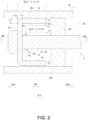
FIG. 2 is an enlarged cross-sectional view of the II-II portion inFIG. 3 , in which main components ofFIG. 1 are enlarged. -
FIG. 3 is a perspective view illustrating the stub tuner and the waveguide tube according to the first embodiment. -
FIG. 4 is a schematic cross-sectional view orthogonal to a tube axis at a portion in which an oscillating electric field is strong in a tube axis direction. -
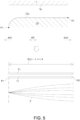
FIG. 5 is a view relating to a transmission path between an inner surface of the waveguide tube and an outer circumferential surface of a second shape. -
FIG. 6 is a view relating to a transmission path between a first conductor and a conductor shaft. -
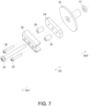
FIG. 7 is a view illustrating an assembly of components forming the stub tuner. -
FIG. 8 is a cross-sectional view of a VIII-VIII portion inFIG. 2 . -
FIG. 9 is a cross-sectional view illustrating a modified example of the first embodiment. -
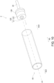
FIG. 10 is a perspective view illustrating a stub tuner and a waveguide tube according to a second embodiment. - In the following, a stub tuner according to the first embodiment of the disclosure is described with reference to the drawings.
- As shown in
FIGs 1 to 3 , astub tuner 2 of the first embodiment is inserted into a tube axial direction inner side AD1 from anopening 10 of awaveguide tube 1 which transmits high frequency waves. Thewaveguide tube 1 is a hollow metal tube, and is formed by using a conductor. Thewaveguide tube 1 is electrically shorted and set to be grounded. The high frequency waves travel in thewaveguide tube 1 from the tube axial direction inner side AD1 toward a tube axial direction outer side AD2. "High frequency waves" in the specification may refer to radio waves of 300 MHz or higher, radio waves of 2 GHz or higher, or radio waves of 3 GHz or higher. Also, as an upper limit value, the high frequency waves may be radio waves of 50 GHz or lower, for example. As the upper limit value, the high frequency waves may also be radio waves of 40 GHz or lower, for example. The high frequency waves may also be microwaves or millimeter waves. Although aluminum or stainless steel is used as the conductor in the embodiment, the disclosure is not limited thereto as long as the conductor is conductive. Thestub tuner 2 is configured to be slidably movable in a tube axial direction AD of thewaveguide tube 1. Accordingly, as shown inFIG. 1 , the position of thestub tuner 2 in the tube axial direction AD in thewaveguide tube 1 is changeable, and an electrical length EL1 from a particular position P0 (seeFIG. 1 ) in thewaveguide tube 1 to atip part 2a of thestub tuner 2 is adjustable. As an example, anothertransmission path 500 or an apparatus may be connected to the particular position P0. - As shown in
FIG. 3 , thewaveguide tube 1 of the first embodiment is arectangular waveguide tube 1 in which a tube cross-section haslong sides 11 andshort sides 12. Thelong sides 11 are parallel to each other, and theshort sides 12 are parallel to each other.FIGs. 1 and2 are cross-sectional views of a II-II portion inFIG. 3 . The cross-sectional views of the II-II portion illustrate a cross-section passing throughcenters 11s of thelong sides 11 and a tube axis A1. In thewaveguide tube 1, an oscillating electric field is generated due to traveling waves and reflected waves.FIG. 4 is a schematic cross-sectional view orthogonal to the tube axis A1 at a portion in which the oscillating electric field is strong in the tube axis direction AD. As shown in the same figure, an oscillating electric field E becomes the antinode at the portion connecting thecenters 11s of thelong sides 11 and becomes the most dominant. Meanwhile, at theshort sides 12, the oscillating electric field E is not generated. The high frequency waves are transmitted in thewaveguide tube 1 in a transverse electric (TE) 10 mode, which is a fundamental mode of suchrectangular waveguide tube 1. In the TE10 mode, the electric field is not generated in a direction parallel to thelong sides 11, but is generated in a direction parallel to theshort sides 12. It is noted that, the disclosure is not limited thereto in a mode other than the fundamental mode (TE10 mode), and a mode other than TE10 may also be used. - As shown in
FIGs. 1 to 3 , thestub tuner 2 has afirst conductor 20 and aconductor shaft 23 having a rod shape, supporting thefirst conductor 20, and extending in the tube axial direction AD. Theconductor shaft 23 is electrically connected to thewaveguide tube 1. Accordingly, thefirst conductor 20 is electrically connected to thewaveguide tube 1 via theconductor shaft 23. As shown inFIGs. 2 and3 , thefirst conductor 20 has afirst shape 21 of a plate shape and asecond shape 22 of a plate shape. Thefirst shape 21 extends in a direction intersecting with the tube axial direction AD in thewaveguide tube 1. Thefirst shape 21 forms areflective surface 21a blocking thewaveguide tube 1 to reflect the high frequency waves. Although thefirst shape 21 blocks thewaveguide tube 1, thefirst shape 21 does not contact the inner surface of thewaveguide tube 1 and a gap is formed. Although thefirst shape 21 in the embodiment extends in a direction orthogonal to the tube axial direction AD, the disclosure is not limited thereto, as long as thefirst shape 21 extends in a direction intersecting with the tube axial direction AD. - As shown in
FIG. 2 , thesecond shape 22 extends from a tube radial direction outer end of thefirst shape 21 toward the tube axial direction outer side AD2 along the tube axial direction AD. An outercircumferential surface 22a of thesecond shape 22 is separated from aninner surface 1b of thewaveguide tube 1. In the embodiment, regarding thefirst conductor 20, two ends of a plate member are bent, the central portion is configured as thefirst shape 21, a pair of bent plate-shaped portions are configured as thesecond shapes 22, and thefirst conductor 20 is formed to exhibit a U-shaped cross-section. As shown inFIG. 3 , thesecond shapes 22 with the shape of a pair of plates faces at least a portion of theinner surface 1b on thelong side 11 of thewaveguide tube 1. Since the oscillating electric field is the most dominant between thecenters 11s of thelong sides 11, as shown inFIG. 4 , thesecond shapes 22 may face thecenters 11s of thelong sides 11 and the vicinities thereof. Specifically, thesecond shape 22 may face at least a region Ar1 that is 24% of a maximum width W1 of thelong side 11 and centers on thecenter 11s of thelong side 11. This is because 60% of power is distributed in the region Ar1 of 24%. In addition, thesecond shape 22 may face at least a region Ar1 that is 36% of the maximum width W1 of thelong side 11 and centers on thecenter 11s of thelong side 11. This is because 81% of power is distributed in the region Ar1 of 36%. Of course, thesecond shape 22 may also face the entireinner surface 1b on thelong side 11. - As shown in
FIG. 2 , although the high frequency waves arriving toward the tube axial direction outer side AD2 are mostly reflected by thereflective surface 21a, the high frequency waves may enter the gap between thesecond shape 22 and theinner surface 1b of thewaveguide tube 1 and leak from the opening of thewaveguide tube 1. In order to suppress the entry of the high frequency waves, a configuration as follows is adopted. - As shown in
FIG. 2 , an electrical length EL2 of the outercircumferential surface 22a of the second shape in the tube axial direction AD is 1/4 of a wavelength λ of the high frequency waves. It suffices as long as the electrical length EL2 is 1/4 of the wavelength λ of the high-frequency waves, with a tube axial direction outer end surface (a surface from P2 to P6) of the outercircumferential surface 22a of thesecond shape 22 as the starting point. Accordingly, as schematically shown inFIG. 5 , a transmission path formed by the metal skin between theinner surface 1b of thewaveguide tube 1 and the outercircumferential surface 22a of thesecond shape 22 can be considered as equivalent to a transmission path T1 with an open end. The electrical length EL2 of the transmission path T1 is 1/4 of the wavelength λ of the high-frequency waves. Due to the traveling waves and reflected waves on the transmission path T1, the oscillating electric field E is generated in thewaveguide tube 1. At a tube axial direction outer end P2 on the outercircumferential surface 22a of thesecond shape 22, the oscillating electric field E becomes an antinode (open). Meanwhile, at a tube axial direction inner end P1 on the outercircumferential surface 22a of thesecond shape 22, the oscillating electric field E becomes a node (short).
As shown inFIG. 2 , the oscillating electric field E may become short at a tube axial direction inner side end part (having a particular range) on the outercircumferential surface 22a of thesecond shape 22. Specifically, the oscillating electric field E may become short in a space from the position P1 to a position Px. In the embodiment, in order for thereflective surface 21a to function strongly as a short plate, the electrical length EL2 of a hypothetical line connecting the position P2 from a position Px2 is set as 1/4 of the wavelength λ. However, it may also be that the electrical length EL2 of a hypothetical line connecting the position P2 from the position Px is set as 1/4 of the wavelength λ. - As shown in
FIG. 2 , in thefirst conductor 20, a distance D2 between the innercircumferential surface 22b of thesecond shape 22 and an outercircumferential surface 23a of theconductor shaft 23 may be longer than a distance D1 between the outercircumferential surface 22a of thesecond shape 22 and theinner surface 1b of thewaveguide tube 1. The performance as a short stub is facilitated. In addition, it is possible to suppress the occurrence of an anomaly that discharge occurs between the second shape and theconductor shaft 23. In particular, since discharge may occur at a high output (60 kW) of a magnetron with a high power at a moment, discharge is prevented effectively. The distance D2 may be 1 mm or more. - As shown in
FIGs. 1 to 3 , thestab tuner 2 has asupport member 24. Thesupport member 24 is provided at theconductor shaft 23 on the side of theopening 10 of thewaveguide tube 1 with respect to thefirst conductor 20. Thesupport member 24 contacts theinner surface 1b of thewaveguide tube 1 and supports thefirst conductor 24 through theconductor shaft 23. It is possible to change the position of thefirst conductor 20 in the tube axial direction AD while bringing thesupport member 24 into contact with theinner surface 1b of thewaveguide tube 1. Thesupport member 24 may be a conductor or not a conductor, as long as thesupport member 24 provides support. Although thesupport member 24 extends in a direction intersecting with the tube axial direction AD and is formed in a plate shape as a whole, the shape is not limited thereto. If the support function is not required, thesupport member 24 may be omitted. - In the embodiment, in the cross-section (see
FIG. 2 ) where thefirst conductor 20 is present, theconductor shaft 23 is located at the center of the pair of second shapes 22. In addition, thesupport member 24 is formed as a conductor and electrically connected to thewaveguide tube 1 via acontact part 24a. A path for electrically connecting thefirst conductor 20 and thewaveguide tube 1 may be arranged via thesupport member 24, and may also be arranged via anadjustment knob 25 to be described afterwards. As shown inFIG. 2 , a space is formed between thefirst conductor 20 and theconductor shaft 23. InFIG. 2 , an intersection point with thesupport member 24 on the outercircumferential surface 23a of theconductor shaft 23 is represented as P3. An intersection point with a tube axial directionouter side surface 21b of thefirst shape 21 on the outercircumferential surface 23a of theconductor shaft 23 is represented as P4. An intersection point with the innercircumferential surface 22b of thesecond shape 22 on the tube axial directionouter side surface 21b of thefirst shape 21 is represented as P5. A tube axial direction outer end of the innercircumferential surface 22b of thesecond shape 22 is represented as P6. In thefirst conductor 20 and theconductor shaft 23, an electrical length EL3 along component surfaces from the intersection point P3 to the tube axial direction outer end P6 through the intersection points P4 and P5 may be 3/4 of the wavelength λ of the high frequency waves. Accordingly, as schematically shown inFIG. 6 , since thesupport member 24 is a conductor and electrically connected with thewaveguide tube 1, it can be considered that a transmission path formed by the metal skin between thefirst conductor 20 and theconductor shaft 23 is equivalent to the transmissions path T2 short-circuited at the end. At the intersection point P3 with thesupport member 24 on the outercircumferential surface 23a of theconductor shaft 23, the oscillating electric field E becomes a node (short). Meanwhile, at the tube axial direction outer end P6 on the innercircumferential surface 22b of thesecond shape 22, the oscillating electric field E becomes an antinode (open). By doing so, as shown inFIG. 2 , in each of the transmission paths formed on the outercircumferential surface 22a and the innercircumferential surface 22b of thesecond shape 22, the oscillating electric field E becomes an antinode at the tube axial direction outer end (P2, P6) of thesecond shape 22. - The
stub tuner 2 can be assembled as shown inFIGs 7 and8 . As shown inFIGs. 7 and8 , in thefirst conductor 20 with a U-shaped cross-section, three non-grooved bolt holes are formed, and in the plate-shapedsupport member 24, three corresponding grooved bolt holes are formed. Two headedbolts 28 are respectively inserted into the bolt holes of thefirst conductor 20 and hollowcylindrical spacers 26, and fastened to the grooved bolt holes of thesupport member 24 . Theconductor shaft 23 is a headed bolt. Theconductor shaft 23 is inserted into the bolt hole of thefirst conductor 20 and fastened to the grooved bolt hole of thesupport member 24. Accordingly, the position relationship between thefirst conductor 20 and thesupport member 24 is fixed. Theconductor shaft 23 is further inserted into a threaded bolt of theadjustment knob 25, and anut 27 is attached to the tip end. Theadjustment knob 25 is associated with theopening 10 of thewaveguide tube 1. By rotating theadjustment knob 25, thefirst conductor 20 advances/treats to configure the position of thefirst conductor 20 in the tube axial direction AD to be adjustable. In the case where thereflective surface 23a of the embodiment is set as short in the embodiment, the electric field becomes zero in all of the upper portion, the intermediate portion, and the lower portion of thewaveguide tube 1. Therefore, the presence/absence of the head constituting theconductor shaft 23 does not affect the performance. Although a headed bolt is used in the embodiment, the disclosure is not limited thereto. In place of the headed bolt, a headless bolt (a fully threaded bolt or a half-threaded bolt with threads on both ends) and a nut may also be adopted. -
FIG. 9 illustrates a modified example of the first embodiment shown inFIGs. 1 to 8 . In thestub tuner 2 according to the modified example of the first embodiment shown inFIG. 9 , an insulatinglayer 3 is provided on the outercircumferential surface 22a of thesecond shape 22. With the presence of the insulatinglayer 3, even if the insulatinglayer 3 contacts theinner surface 1b of thewaveguide tube 1, it is possible to ensure that the outercircumferential surface 22a of thesecond shape 22 is separated from theinner surface 1b of thewaveguide tube 1. If the insulatinglayer 3 is provided, even if thefirst conductor 20 and thewaveguide tube 1 contact when thestub tuner 2 is inserted into thewaveguide tube 1, thefirst conductor 20 and thewaveguide tube 1 can be prevented from electrically contacting each other. Accordingly, the assembling process can be simplified. The insulatinglayer 3 may be any component as long as such component exhibits an electrically insulating effect. Examples of the insulatinglayer 3 include attachment of an insulating sheet having an adhesive. - A stub tuner of a second embodiment will be described. Components same as those of the first embodiment are labeled with the same reference symbols, and the descriptions thereof will be omitted. As shown in
FIG. 2 , thestub tuner 2 of the second embodiment is inserted into acircular waveguide tube 101 in which a tube cross-section is circular. In the first embodiment, thesecond shape 22 is an elongated member with a U-shaped cross-section. However, in the second embodiment, asecond shape 122 is in a cylindrical shape. A first conductor 120 (afirst shape 121 and the second shape 122) is formed to be line symmetric with theconductor shaft 23 as an axis of symmetry. In thefirst conductor 120, in any cross-section passing through theconductor shaft 23, thefirst shape 121 and thesecond shape 122 are formed with a U-shaped cross-section. Thesupport member 124 is formed in a disc shape in accordance with the inner circumferential surface of thecircular waveguide tube 101. Other than the above, the second embodiment is the same as the first embodiment. - According to the above, in the first and second embodiments shown in
FIGs. 1 to 10 , astub tuner 2 may include a first conductor (20, 120) and aconductor shaft 23. The first conductor (20, 120) is inserted from anopening 10 of a waveguide tube (1, 101) transmitting high frequency waves to a tube axial direction inner side AD1 and includes a first shape (21, 121) and a second shape (22, 122). The first shape (21, 121) is a plate shape extending in a direction intersecting with the tube axial direction AD in the waveguide tube. The second shape (22, 122) is a plate shape extending along the tube axial direction AD from a tube axial direction outer end of the first shape toward a tube axial direction outer side AD2. An outercircumferential surface 22a of the second shape is separated from aninner surface 1b of thewaveguide tube 1, and an electrical length EL2 along the tube axial direction AD on the outercircumferential surface 22a of the second shape is 1/4 of a wavelength λ of the high frequency waves. Theconductor 23 has a rod shape, is electrically connected to the waveguide tube, supports the first conductor, and extends in the tube axial direction AD. - In this way, since the outer
circumferential surface 22a of the second shape (22, 122) is separated from theinner surface 1b of the waveguide tube (1, 101), the transmission path can be considered as equivalent to the transmission path T1 with an open end. In addition, since the electrical length EL2 along the tube axial direction AD on the outercircumferential surface 22a of the second end (22, 122) is 1/4 of the wavelength λ of the high frequency waves, the oscillating electric field E generated in the waveguide tube (1, 101) becomes an antinode at the axial direction outer end P2 on the outercircumferential surface 22a of the second shape (22, 122). The oscillating electric field E generated in the waveguide tube (1, 101) becomes a node at the axial direction inner end P1 on the outercircumferential surface 22a of the second shape (22, 122). Since the node portion of the oscillating electric field E is arranged at the inlet of the gap between the second shape (22, 122) and theinner surface 1b of the waveguide tube (1, 101), the radio waves entering between the second shape (22, 122) and the inner surface of the waveguide tube (1, 101) can be significantly suppressed, and radio wave leakage as well as discharge between the second shape (22, 122) and the waveguide tube (1, 101) can be prevented.
In addition, since the second shape (22, 122) is separated from theinner surface 1b of the waveguide tube (1, 101), the outer diameter of the first conductor (20, 120) is smaller than the inner diameter of the waveguide tube, and, compared with a configuration in which the inner diameter of the waveguide tube and the outer diameter of the first conductor are the same, the first conductor (20, 120) can be moved with a smaller operation force during position adjustment. Moreover, the generation of metal powder due to contact between the first conductor (20, 120) and the waveguide tube (1, 101) can be reduced or prevented, and it is possible to suppress a failure. - Although the disclosure is not particularly limited, according to the first and second embodiments shown in
FIGs. 1 to 10 , it may also be that in the first conductor (20, 120), a distance D2 between an innercircumferential surface 22b of the second shape (22, 122) and an outercircumferential surface 23a of theconductor shaft 23 is greater than a distance D1 between the outercircumferential surface 22a of the second shape (22, 122) and aninner surface 1b of the waveguide tube (1, 101). - According to such configuration, by reducing the electric field between the inner
circumferential surface 22b of the second shape (22, 122) and the outercircumferential surface 23a of theconductor shaft 23, the electrical field difference with respect to theinner surface 1b of the waveguide tube (1, 101), which occurs on the outercircumferential surface 22a of the second shape (22, 122), acts strongly, and the performance as a short stub is facilitated. In addition, it is possible to suppress the occurrence of an anomaly that discharge occurs between the innercircumferential surface 22b of the second shape (22, 122) and the outercircumferential surface 23a of theconductor shaft 23. - Although the disclosure is not particularly limited, according to the first and second embodiments shown in
FIGs. 1 to 10 , it may also be that the stub tuner includes a support member (24, 124) provided at theconductor shaft 23 on a side of theopening 10 of the waveguide tube (1, 101) with respect to the first conductor (20, 120), contacting aninner surface 1b of the waveguide tube to pass through theconductor shaft 23 to support the first conductor. - According to the configuration, since the position of the first conductor (20, 120) in the tube axial direction AD can be changed while the support member (24, 124) is brought into contact with the
inner surface 1b of the waveguide tube (1, 101), it is possible facilitate the operability. - Although the disclosure is not particularly limited, according to the first and second embodiments shown in
FIGs. 1 to 10 , it may also be that in a cross-section where the first conductor (20, 120) is present, theconductor shaft 23 is located at a center of a pair of the second shapes (22, 122), the support member (24, 124) is formed by a conductor and electrically connected to the conductor tube (1, 101), in the first conductor (20, 120) and theconductor shaft 23, an electrical length EL3 along component surfaces from an intersection point P3 with the support member (24, 124) on an outercircumferential surface 23a of theconductor shaft 23 to a tube axial direction outer end P6 of an innercircumferential surface 22b of the second shape (22, 122) through an intersection point P4 with a tube axial directionouter side surface 21b of the first shape (21, 121) on an outercircumferential surface 23a of theconductor shaft 23 and an intersection point P5 with the innercircumferential surface 22b of the second shape (22, 122) on the tube axial directionouter side surface 21b of the first shape (21, 121) is 3/4 of the wavelength λ of the high frequency waves. - According to the configuration, since the support member (24, 124) is a conductor and electrically connected to the waveguide tube (1, 101), the oscillating electric field E becomes a node at the intersection point P3. With the transmission path T2 formed by the metal skin on the inner circumferential side of the second shape from the intersection point P3 to the intersection point P6 via the intersection points P4 and P5, the oscillating electric field E becomes an antinode at the tube axial direction outer end P6 of the inner
circumferential surface 22b of the second shape (22, 122). Meanwhile, the electrical length EL2 along the tube axial direction AD on the outercircumferential surface 22a of the second shape (22, 122) is 1/4 of the wavelength λ of the high frequency waves, and, with the transmission path T1 formed between the outercircumferential surface 22a of the second shape (22, 122) and theinner surface 1b of the waveguide tube (1, 101), the oscillating electric field E at the tube axial direction outer end P2 of the outer circumferential surface of the second shape becomes an antinode. By doing so, in each of the transmission paths (T1, T2) formed on the outer circumferential side and the inner circumferential side of the second shape (22, 122), the oscillating electric field E becomes an antinode at the tube axial direction outer end (P2, P6) of the second shape. As a result, the oscillating electric field E becoming a node in the tube axial direction inner end P1 on the outercircumferential surface 22a of the second shape (22, 122) can be facilitated, and it is possible to facilitate a radio wave shielding effect. - Although the disclosure is not particularly limited, according to the embodiment shown in
FIG. 8 , it may also be that an insulatinglayer 3 is provided on the outercircumferential surface 22a of thesecond shape 22. - With the configuration, even if the
second shape 22 mechanically contact theinner surface 1b of thewaveguide tube 1 when thefirst conductor 20 is inserted into thewaveguide tube 1, it is possible to suppress collapse of the electrical length EL2, as thesecond shape 22 and thewaveguide tube 1 are not in electric contact due to the insulatinglayer 3. - Although the disclosure is not particularly limited, according to the first embodiment shown in
FIGs. 1 to 9 , it may also be that thewaveguide tube 1 is a rectangular waveguide tube in which a tube cross-sectional surface haslong sides 11 andshort sides 12, thesecond shape 22 is a shape of a pair of plates respectively extending from a tube axial direction outer end of thefirst shape 21 toward theopening 10 along the tube axial direction AD, and the shape of the pair of plates faces at least a portion of theinner surface 1b on thelong sides 11 of thewaveguide tube 1. - According to the configuration, it is possible to suitably suppress leakage of the high frequency waves in the
rectangular waveguide tube 1. In addition, it is not required that the entire inner surface on thelong sides 11 facessecond shape 2, and the design and adjustment are simplified. - Although the disclosure is not particularly limited, according to the first embodiment shown in
FIGs. 1 to 9 , it may also be that in a cross-section passing throughcenters 11s of thelong sides 11 and a tube axis A1, thefirst conductor 20 is in a U shape. - According to the configuration, since the portion passing through the
centers 11s of thelong sides 11 and the tube axis A1 in therectangular waveguide tube 1 is a portion with the maximum electric field, it is possible to reliably exhibit the effects. - Although the disclosure is not particularly limited, according to the second embodiment shown in
FIG. 10 , it may also be that the waveguide tube is acircular waveguide tube 101 in which a tube cross-sectional surface is circular, and thesecond shape 122 is formed to be line symmetric with theconductor shaft 23 as an axis of symmetry. - According to the configuration, in the
circular waveguide tube 101, the electric field is at the maximum along any tube axial direction passing through the tube axis A1. Therefore, it is possible to reliably exhibit the effects. - Although the embodiments of the disclosure have been described above based on the drawings, it should be considered that the specific configurations are not limited to these embodiments. The scope of the disclosure is indicated not only by the description of the above embodiments but also by the scope of claims, and includes all modifications within the meaning and scope equivalent to the scope of claims.
- It is possible to adopt the structure adopted in each of the above embodiments in any other embodiment.
- The specific configuration of each part is not limited to the above embodiments, and various modifications are possible without departing from the scope of the disclosure.
-
- 1: Rectangular waveguide tube (waveguide tube);
- 11: Long side;
- 12: Short side;
- 101: Circular waveguide tube (waveguide tube);
- 10: Opening;
- 20: First conductor;
- 21: First shape;
- 22: Second shape;
- 23: Conductor shaft;
- 24: Support member;
- 3: Insulating layer;
- AD: Tube axial direction;
- AD1: Tube axial direction inner side;
- AD2: Tube axial direction outer side.
Claims (8)
- A stub tuner, comprising:a first conductor, inserted from an opening of a waveguide tube transmitting high frequency waves to a tube axial direction inner side and comprising: a first shape, which is a plate shape extending in a direction intersecting with the tube axial direction in the waveguide tube; and a second shape, which is a plate shape extending along the tube axial direction from a tube axial direction outer end of the first shape toward a tube axial direction outer side, wherein an outer circumferential surface of the second shape is separated from an inner surface of the waveguide tube, and an electrical length along the tube axial direction on the outer circumferential surface of the second shape is 1/4 of a wavelength of the high frequency waves; anda conductor shaft, having a rod shape, electrically connected to the waveguide tube, supporting the first conductor, and extending in the tube axial direction.
- The stub tuner as claimed in claim 1, wherein in the first conductor, a distance between an inner circumferential surface of the second shape and an outer circumferential surface of the conductor shaft is greater than a distance between the outer circumferential surface of the second shape and the inner surface of the waveguide tube.
- The stub tuner as claimed in claim 1 or 2, comprising a support member provided at the conductor shaft on an opening side of the waveguide tube with respect to the first conductor, and contacting an inner surface of the waveguide tube to pass through the conductor shaft to support the first conductor.
- The stub tuner as claimed in claim 3, wherein in a cross-section where the first conductor is present, the conductor shaft is located at a center of a pair of the second shapes,the support member is formed by a conductor and electrically connected to the conductor tube,in the first conductor and the conductor shaft, an electrical length along component surfaces from an intersection point P3 with the support member on an outer circumferential surface of the conductor shaft to a tube axial direction outer end P6 of an inner circumferential surface of the second shape through an intersection point P4 with a tube axial direction outer side surface of the first shape on an outer circumferential surface of the conductor shaft and an intersection point P5 with the inner circumferential surface of the second shape on the tube axial direction outer side surface of the first shape is 3/4 of the wavelength of the high frequency waves.
- The stub tuner as claimed in any one of claims 1 to 4, wherein an insulating layer is provided on the outer circumferential surface of the second shape.
- The stub tuner as claimed in any one of claims 1 to 5, wherein the waveguide tube is a rectangular waveguide tube in which a tube cross-sectional surface has long sides and short sides,
the second shape is a shape of a pair of plates respectively extending from a tube axial direction outer end of the first shape toward the opening along the tube axial direction, and the shape of the pair of plates faces at least a portion of the inner surface on the long sides of the waveguide tube. - The stub tuner as claimed in claim 6, wherein in a cross-section passing through central portions of the long sides and a tube axis, the first conductor is in a U shape.
- The stub tuner as claimed in any one of claims 1 to 5, wherein the waveguide tube is a circular waveguide tube in which a tube cross-sectional surface is circular, and
the second shape is formed to be line symmetric with the conductor shaft as an axis of symmetry.
Applications Claiming Priority (2)
| Application Number | Priority Date | Filing Date | Title |
|---|---|---|---|
| JP2020173720 | 2020-10-15 | ||
| PCT/JP2021/033884 WO2022080074A1 (en) | 2020-10-15 | 2021-09-15 | Stub tuner |
Publications (2)
| Publication Number | Publication Date |
|---|---|
| EP4231441A1 true EP4231441A1 (en) | 2023-08-23 |
| EP4231441A4 EP4231441A4 (en) | 2024-10-30 |
Family
ID=81209098
Family Applications (1)
| Application Number | Title | Priority Date | Filing Date |
|---|---|---|---|
| EP21879816.3A Withdrawn EP4231441A4 (en) | 2020-10-15 | 2021-09-15 | REACTANCE ARM |
Country Status (4)
| Country | Link |
|---|---|
| US (1) | US20230198113A1 (en) |
| EP (1) | EP4231441A4 (en) |
| CN (1) | CN115885425A (en) |
| WO (1) | WO2022080074A1 (en) |
Family Cites Families (15)
| Publication number | Priority date | Publication date | Assignee | Title |
|---|---|---|---|---|
| US3049684A (en) * | 1961-02-13 | 1962-08-14 | Frank E Vaccaro | Choke type shorting plunger |
| GB1145267A (en) * | 1965-07-01 | 1969-03-12 | Emi Ltd | Improvements in or relating to short circuiting plungers for high frequency lines |
| JPS5013464Y1 (en) * | 1970-01-23 | 1975-04-24 | ||
| JPS6010088Y2 (en) * | 1980-03-06 | 1985-04-08 | 島田理化工業株式会社 | Waveguide type variable short circuit |
| JPS57204702U (en) * | 1981-06-22 | 1982-12-27 | ||
| JPS5813701U (en) * | 1981-07-16 | 1983-01-28 | 三菱電機株式会社 | waveguide device |
| JPS58125401U (en) * | 1982-02-18 | 1983-08-26 | 三菱電機株式会社 | Short circuit conductor |
| JPH03105002U (en) * | 1990-02-14 | 1991-10-31 | ||
| US5138289A (en) * | 1990-12-21 | 1992-08-11 | California Institute Of Technology | Noncontacting waveguide backshort |
| JPH07106808A (en) * | 1993-10-06 | 1995-04-21 | Power Reactor & Nuclear Fuel Dev Corp | High frequency transmission element |
| JP3583478B2 (en) | 1994-08-30 | 2004-11-04 | 株式会社ダイヘン | Movable stub tuner for microwave |
| JPH08191156A (en) * | 1995-01-10 | 1996-07-23 | Fujitsu Ltd | SIS mixer and ozone measuring device using the same |
| JP4837854B2 (en) * | 2001-09-28 | 2011-12-14 | 東京エレクトロン株式会社 | Matching device and plasma processing apparatus |
| JP2010168684A (en) * | 2009-01-22 | 2010-08-05 | Micro Denshi Kk | Microwave drawing machine |
| JP6567646B2 (en) | 2015-02-25 | 2019-08-28 | 国立大学法人大阪大学 | Microwave plasma gas phase reactor |
-
2021
- 2021-09-15 EP EP21879816.3A patent/EP4231441A4/en not_active Withdrawn
- 2021-09-15 WO PCT/JP2021/033884 patent/WO2022080074A1/en not_active Ceased
- 2021-09-15 CN CN202180052142.0A patent/CN115885425A/en not_active Withdrawn
-
2023
- 2023-02-23 US US18/173,750 patent/US20230198113A1/en not_active Abandoned
Also Published As
| Publication number | Publication date |
|---|---|
| WO2022080074A1 (en) | 2022-04-21 |
| EP4231441A4 (en) | 2024-10-30 |
| US20230198113A1 (en) | 2023-06-22 |
| CN115885425A (en) | 2023-03-31 |
Similar Documents
| Publication | Publication Date | Title |
|---|---|---|
| EP0455485B1 (en) | Spatial field power combiner | |
| EP2330681A1 (en) | Compact OMT device | |
| US20140340271A1 (en) | Antenna Array with Reduced Mutual Coupling Between Array Elements | |
| WO2008053886A1 (en) | Waveguide connection structure | |
| EP4047739B1 (en) | Waveguide connecting structure | |
| JP2011217251A (en) | Nrd guide modulator | |
| EP4231441A1 (en) | Stub tuner | |
| CN112820610A (en) | Energy transmission coupling structure for ribbon-shaped beam staggered grid traveling wave tube | |
| CN110165348B (en) | High-power millimeter wave TE01Mode filter | |
| CN114256568B (en) | High-power multimode broadband rotary joint | |
| EP0660363B1 (en) | Linear-beam cavity circuits with non-resonant RF loss slabs | |
| CN107863593B (en) | Circular waveguide suppressor for suppressing TE11 mode microwave and its design method | |
| JP7695840B2 (en) | Waveguide connection material | |
| US2798981A (en) | Traveling wave electron discharge devices | |
| EP4287393A1 (en) | Waveguide tube connecting member | |
| CN223206437U (en) | Waveguide conversion device | |
| CN107134657B (en) | Microwave absorbing device for periodically distributed confocal waveguide dielectric ceramic rings | |
| US20250112377A1 (en) | Microwave antenna systems with multiple waveguide segments | |
| US2967974A (en) | Magnetron output coupler | |
| RU2774737C1 (en) | Pluggable connection for combined coaxial and circular waveguides of the reflector antenna feed | |
| US20070040629A1 (en) | Nrd guide converter and connected structure of dielectric and conductor | |
| CN121812914A (en) | A dual-condition coaxial input coupler suitable for high-power cyclotron amplifiers | |
| Liu | Optimum design for RF windows in millimeter wave high power tubes | |
| Rakshit et al. | Design of coaxial rotary joint using an overmoded coaxial cavity with developed single channel prototype | |
| CN121331721A (en) | A broadband super-radiation backwave tube axial energy extraction structure |
Legal Events
| Date | Code | Title | Description |
|---|---|---|---|
| STAA | Information on the status of an ep patent application or granted ep patent |
Free format text: STATUS: THE INTERNATIONAL PUBLICATION HAS BEEN MADE |
|
| PUAI | Public reference made under article 153(3) epc to a published international application that has entered the european phase |
Free format text: ORIGINAL CODE: 0009012 |
|
| STAA | Information on the status of an ep patent application or granted ep patent |
Free format text: STATUS: REQUEST FOR EXAMINATION WAS MADE |
|
| 17P | Request for examination filed |
Effective date: 20230330 |
|
| AK | Designated contracting states |
Kind code of ref document: A1 Designated state(s): AL AT BE BG CH CY CZ DE DK EE ES FI FR GB GR HR HU IE IS IT LI LT LU LV MC MK MT NL NO PL PT RO RS SE SI SK SM TR |
|
| DAV | Request for validation of the european patent (deleted) | ||
| DAX | Request for extension of the european patent (deleted) | ||
| REG | Reference to a national code |
Ref country code: DE Ref legal event code: R079 Free format text: PREVIOUS MAIN CLASS: H01P0005040000 Ipc: H01P0001280000 |
|
| A4 | Supplementary search report drawn up and despatched |
Effective date: 20240927 |
|
| RIC1 | Information provided on ipc code assigned before grant |
Ipc: H01P 1/28 20060101AFI20240923BHEP |
|
| STAA | Information on the status of an ep patent application or granted ep patent |
Free format text: STATUS: THE APPLICATION IS DEEMED TO BE WITHDRAWN |
|
| 18D | Application deemed to be withdrawn |
Effective date: 20250416 |