EP4231024A1 - Apparatus and method for measuring strength of signal - Google Patents
Apparatus and method for measuring strength of signal Download PDFInfo
- Publication number
- EP4231024A1 EP4231024A1 EP21898680.0A EP21898680A EP4231024A1 EP 4231024 A1 EP4231024 A1 EP 4231024A1 EP 21898680 A EP21898680 A EP 21898680A EP 4231024 A1 EP4231024 A1 EP 4231024A1
- Authority
- EP
- European Patent Office
- Prior art keywords
- voltage
- transmission line
- power
- signal
- antenna
- Prior art date
- Legal status (The legal status is an assumption and is not a legal conclusion. Google has not performed a legal analysis and makes no representation as to the accuracy of the status listed.)
- Pending
Links
- 238000000034 method Methods 0.000 title claims abstract description 46
- 230000005540 biological transmission Effects 0.000 claims abstract description 187
- 238000004891 communication Methods 0.000 claims abstract description 29
- 238000012546 transfer Methods 0.000 abstract description 4
- 230000007774 longterm Effects 0.000 abstract description 2
- 230000008859 change Effects 0.000 description 41
- 238000012545 processing Methods 0.000 description 14
- 238000005259 measurement Methods 0.000 description 11
- 230000010287 polarization Effects 0.000 description 10
- 238000013459 approach Methods 0.000 description 5
- 230000006870 function Effects 0.000 description 5
- 238000010276 construction Methods 0.000 description 4
- 230000008878 coupling Effects 0.000 description 4
- 238000010168 coupling process Methods 0.000 description 4
- 238000005859 coupling reaction Methods 0.000 description 4
- 238000010586 diagram Methods 0.000 description 4
- 239000003990 capacitor Substances 0.000 description 2
- 230000008569 process Effects 0.000 description 2
- 239000000758 substrate Substances 0.000 description 2
- 238000010897 surface acoustic wave method Methods 0.000 description 2
- 230000015572 biosynthetic process Effects 0.000 description 1
- 238000007796 conventional method Methods 0.000 description 1
- 238000013461 design Methods 0.000 description 1
- 230000000694 effects Effects 0.000 description 1
- 238000005516 engineering process Methods 0.000 description 1
- 238000001914 filtration Methods 0.000 description 1
- 239000007769 metal material Substances 0.000 description 1
- 230000003287 optical effect Effects 0.000 description 1
- 230000008054 signal transmission Effects 0.000 description 1
- 238000003786 synthesis reaction Methods 0.000 description 1
Images


Classifications
-
- G—PHYSICS
- G01—MEASURING; TESTING
- G01R—MEASURING ELECTRIC VARIABLES; MEASURING MAGNETIC VARIABLES
- G01R22/00—Arrangements for measuring time integral of electric power or current, e.g. electricity meters
- G01R22/06—Arrangements for measuring time integral of electric power or current, e.g. electricity meters by electronic methods
-
- H—ELECTRICITY
- H01—ELECTRIC ELEMENTS
- H01Q—ANTENNAS, i.e. RADIO AERIALS
- H01Q3/00—Arrangements for changing or varying the orientation or the shape of the directional pattern of the waves radiated from an antenna or antenna system
- H01Q3/44—Arrangements for changing or varying the orientation or the shape of the directional pattern of the waves radiated from an antenna or antenna system varying the electric or magnetic characteristics of reflecting, refracting, or diffracting devices associated with the radiating element
- H01Q3/443—Arrangements for changing or varying the orientation or the shape of the directional pattern of the waves radiated from an antenna or antenna system varying the electric or magnetic characteristics of reflecting, refracting, or diffracting devices associated with the radiating element varying the phase velocity along a leaky transmission line
-
- G—PHYSICS
- G01—MEASURING; TESTING
- G01R—MEASURING ELECTRIC VARIABLES; MEASURING MAGNETIC VARIABLES
- G01R29/00—Arrangements for measuring or indicating electric quantities not covered by groups G01R19/00 - G01R27/00
- G01R29/08—Measuring electromagnetic field characteristics
- G01R29/0864—Measuring electromagnetic field characteristics characterised by constructional or functional features
- G01R29/0878—Sensors; antennas; probes; detectors
-
- G—PHYSICS
- G01—MEASURING; TESTING
- G01R—MEASURING ELECTRIC VARIABLES; MEASURING MAGNETIC VARIABLES
- G01R1/00—Details of instruments or arrangements of the types included in groups G01R5/00 - G01R13/00 and G01R31/00
- G01R1/30—Structural combination of electric measuring instruments with basic electronic circuits, e.g. with amplifier
-
- G—PHYSICS
- G01—MEASURING; TESTING
- G01R—MEASURING ELECTRIC VARIABLES; MEASURING MAGNETIC VARIABLES
- G01R19/00—Arrangements for measuring currents or voltages or for indicating presence or sign thereof
- G01R19/003—Measuring mean values of current or voltage during a given time interval
-
- G—PHYSICS
- G01—MEASURING; TESTING
- G01R—MEASURING ELECTRIC VARIABLES; MEASURING MAGNETIC VARIABLES
- G01R19/00—Arrangements for measuring currents or voltages or for indicating presence or sign thereof
- G01R19/10—Measuring sum, difference or ratio
-
- G—PHYSICS
- G01—MEASURING; TESTING
- G01R—MEASURING ELECTRIC VARIABLES; MEASURING MAGNETIC VARIABLES
- G01R19/00—Arrangements for measuring currents or voltages or for indicating presence or sign thereof
- G01R19/30—Measuring the maximum or the minimum value of current or voltage reached in a time interval
-
- G—PHYSICS
- G01—MEASURING; TESTING
- G01R—MEASURING ELECTRIC VARIABLES; MEASURING MAGNETIC VARIABLES
- G01R29/00—Arrangements for measuring or indicating electric quantities not covered by groups G01R19/00 - G01R27/00
- G01R29/08—Measuring electromagnetic field characteristics
- G01R29/0864—Measuring electromagnetic field characteristics characterised by constructional or functional features
- G01R29/0892—Details related to signal analysis or treatment; presenting results, e.g. displays; measuring specific signal features other than field strength, e.g. polarisation, field modes, phase, envelope, maximum value
-
- H—ELECTRICITY
- H01—ELECTRIC ELEMENTS
- H01Q—ANTENNAS, i.e. RADIO AERIALS
- H01Q9/00—Electrically-short antennas having dimensions not more than twice the operating wavelength and consisting of conductive active radiating elements
- H01Q9/04—Resonant antennas
- H01Q9/16—Resonant antennas with feed intermediate between the extremities of the antenna, e.g. centre-fed dipole
- H01Q9/28—Conical, cylindrical, cage, strip, gauze, or like elements having an extended radiating surface; Elements comprising two conical surfaces having collinear axes and adjacent apices and fed by two-conductor transmission lines
-
- H—ELECTRICITY
- H03—ELECTRONIC CIRCUITRY
- H03F—AMPLIFIERS
- H03F1/00—Details of amplifiers with only discharge tubes, only semiconductor devices or only unspecified devices as amplifying elements
- H03F1/02—Modifications of amplifiers to raise the efficiency, e.g. gliding Class A stages, use of an auxiliary oscillation
- H03F1/0205—Modifications of amplifiers to raise the efficiency, e.g. gliding Class A stages, use of an auxiliary oscillation in transistor amplifiers
- H03F1/0288—Modifications of amplifiers to raise the efficiency, e.g. gliding Class A stages, use of an auxiliary oscillation in transistor amplifiers using a main and one or several auxiliary peaking amplifiers whereby the load is connected to the main amplifier using an impedance inverter, e.g. Doherty amplifiers
-
- H—ELECTRICITY
- H03—ELECTRONIC CIRCUITRY
- H03F—AMPLIFIERS
- H03F3/00—Amplifiers with only discharge tubes or only semiconductor devices as amplifying elements
- H03F3/189—High-frequency amplifiers, e.g. radio frequency amplifiers
-
- H—ELECTRICITY
- H03—ELECTRONIC CIRCUITRY
- H03F—AMPLIFIERS
- H03F3/00—Amplifiers with only discharge tubes or only semiconductor devices as amplifying elements
- H03F3/20—Power amplifiers, e.g. Class B amplifiers, Class C amplifiers
- H03F3/24—Power amplifiers, e.g. Class B amplifiers, Class C amplifiers of transmitter output stages
-
- G—PHYSICS
- G01—MEASURING; TESTING
- G01R—MEASURING ELECTRIC VARIABLES; MEASURING MAGNETIC VARIABLES
- G01R21/00—Arrangements for measuring electric power or power factor
- G01R21/06—Arrangements for measuring electric power or power factor by measuring current and voltage
-
- H—ELECTRICITY
- H03—ELECTRONIC CIRCUITRY
- H03F—AMPLIFIERS
- H03F2200/00—Indexing scheme relating to amplifiers
- H03F2200/451—Indexing scheme relating to amplifiers the amplifier being a radio frequency amplifier
Definitions
- the disclosure relates, in general, to a wireless communication system, and in particular, to a method and apparatus for measuring strength of a signal in the wireless communication system.
- the 5G communication system or the pre-5G communication system is called a beyond 4G network communication system or a post Long Term Evolution (LTE) system.
- LTE Long Term Evolution
- the 5G communication system is considered to be implemented in an ultra-high frequency band.
- beamforming massive Multiple Input Multiple Output (MIMO), full dimensional MIMO (FD-MIMO), array antenna, analog beam-forming, and large scale antenna techniques are under discussion in the 5G communication system.
- MIMO massive Multiple Input Multiple Output
- FD-MIMO full dimensional MIMO
- array antenna analog beam-forming, and large scale antenna techniques are under discussion in the 5G communication system.
- FQAM Frequency shift keying and Quadrature Amplitude Modulation
- SWSC Sliding Window Superposition Coding
- ACM Advanced Coding Modulation
- FBMC Filter Bank Multi Carrier
- NOMA Non Orthogonal Multiple Access
- SCMA Sparse Code Multiple Access
- a beamforming technique may be used when using a signal of a millimeter wave (mmWave) band in the wireless communication system.
- An electronic device performing beamforming may require a plurality of antenna elements, and may require a plurality of Radio Frequency (RF) chains as paths through which signals transmitted or received by the plurality of antenna elements pass.
- RF Radio Frequency
- the electronic device may need to minimize power consumption. Accordingly, in order to measure power consumed by the signals transmitted or received by the plurality of antenna elements through the plurality of RF chains, there is a need to measure power consumption for each RF chain.
- the disclosure provides a method and apparatus in which a transmission line having a specific length is used to accurately measure power of a signal passing through the transmission line in a wireless communication system.
- the disclosure provides a structure capable of accurately measuring signal power by arranging a transmission line without having to use an additional device in the wireless communication system.
- a method of measuring power of a signal may include obtaining, by at least one sensor, a first voltage of the signal at a first point between a power amplifier and a transmission line, obtaining, by the at least one sensor, a second voltage of the signal at a second point between the transmission line and an antenna, and calculating power, based on the first voltage and the second voltage.
- a length of the transmission line may be associated with a wavelength of the signal.
- an electronic device of a wireless communication system may include a power amplifier, an antenna, a transmission line, at least one sensor, and at least one processor electrically coupled to the at least one sensor.
- the at least one sensor may be configured to obtain a first voltage of a signal at a first point between the power amplifier and the transmission line, and obtain a second voltage of the signal at a second point between the transmission line and the antenna.
- the at least one processor may be configured to calculate power, based on the first voltage and second voltage obtained by the at least one sensor.
- a length of the transmission line may be associated with a wavelength of the signal.
- an electronic device of a wireless communication system may include a plurality of Radio Frequency (RF) chains, a plurality of antennas corresponding to the plurality of RF chains, a transmission line, at least one sensor, and at least one processor electrically coupled to the at least one sensor.
- at least one RF chain may include a power amplifier.
- the transmission line may be disposed between the power amplifier and at least one antenna corresponding to the power amplifier.
- the at least one sensor may be configured to obtain a first voltage of a signal at a first point between the power amplifier and the transmission line, and obtain a second voltage of the signal at a second point between the at least one antenna and the transmission line.
- the at least one processor may be configured to calculate power, based on the first voltage and second voltage obtained by the at least one sensor.
- a length of the transmission line may be associated with a wavelength of the signal.
- An apparatus and method measure voltages of a signal passing through a specific-length transmission line disposed between a power amplifier and an antenna, thereby accurately calculating power irrespective of a change in antenna impedance.
- An apparatus and method according to various embodiments of the disclosure use a specific power amplifier, thereby accurately calculating power without having to dispose an additional transmission line.
- a hardware-based approach is described for example in the various embodiments of the disclosure described hereinafter. However, since the various embodiments of the disclosure include a technique in which hardware and software are both used, a softwarebased approach is not excluded in the embodiments of the disclosure.
- an electronic device e.g., a board structure, a substrate, a Printed Circuit Board (PCB), a Flexible PCB (FPCB), a module, an antenna, an antenna element, a circuit, a processor, a chip, a component, and a device
- terms used to refer to a shape of the parts e.g., a construction body, a construction object, a support portion, a contact portion, a protrusion, and an opening
- terms used to refer to a connection portion between the construction bodies e.g., a connection line, a feeding line, a connection portion, a contact portion, a support portion, a contact construction body, a conductive member, an assembly
- terms used to refer to a circuitry e.g., a PCB, an FPCB, a signal line, a feeding line, a data line, an RF signal line, an antenna line, an RF path, an RF module, and an RF circuit
- a sensor disposed to an Integrated Circuit (IC) inside the RF chain has been used to measure power of a signal transmitted from an antenna.
- the power is calculated indirectly through a signal voltage measured through the sensor.
- the impedance of the antenna may be changed in practice due to an external factor (e.g., an arrangement of an adjacent circuit) or the like, and thus it may be inaccurate to measure the signal power by using only the signal voltage.
- the disclosure proposes a structure for accurately measuring power of a signal passing through an RF chain even in an environment in which impedance of an antenna changes.
- a transmission line having a specific length is disposed between the antenna and a power amplifier disposed on the RF chain, and a sensor obtains voltages of signals at front and rear end of the transmission line having the specific length. Therefore, the electronic device may more accurately measure power of the signal, based on the obtained voltages.
- FIG. 1 illustrates an example of an electronic device according to an embodiment of the disclosure.
- an electronic device including one power amplifier, one antenna, one transmission line coupling the power amplifier and the antenna, one sensor, and one Analog to Digital Converter (ADC) & Modulation and demodulation (Modem) is illustrated in FIG. 1 for convenience of description, the disclosure is not limited thereto.
- the power amplifier and the antenna may be coupled by a plurality of transmission lines.
- the electronic device may include a plurality of power amplifiers, as described below with reference to FIG. 2 .
- the plurality of sensors may be coupled to the transmission line.
- an electronic device 100 may include a Power Amplifier (PA) 110, a Transmission Line (T/L) 120, an antenna 140, a sensor 150, an Analog to digital Converter & Modulation and demodulation (ADC & Modem) 160.
- the PA 110 may be disposed on a plurality of RF chains in the electronic device 100 including the plurality of RF chains, as described below with reference to FIG. 8 .
- the PA 110 may be disposed on at least one RF chain among the plurality of RF chains.
- the PA 110 may be disposed only on one RF chain among the plurality of RF chains.
- the PA 110 may be disposed only on some adjacent RF chains among the plurality of RF chains.
- the PA 110 may be disposed only any RF chains among the plurality of RF chains.
- the PA 110 may be coupled to the transmission line 120.
- the PA 110 may be coupled to one end of the transmission line 120 only at any one portion referred to as a first connection portion 131.
- the PA 110 may be coupled to the plurality of transmission lines 120.
- the PA 110 may be coupled to two or more transmission lines 120.
- the PA 110 may be constructed of a plurality of power amplifiers.
- the PA 110 may be constructed of a Doherty power amplifier including two power amplifiers.
- one end of the transmission line 120 may be coupled to an output stage of the PA 110, and the other end of the transmission line 120 may be coupled to the antenna 140.
- any one portion between the transmission line 120 and the output stage of the PA 110 may be referred to as the first connection portion 131, and any one portion between the transmission line 120 and the antenna 140 may be referred to as a second connection portion 132.
- the transmission line 120 may be a path for transmitting to the antenna 140 a signal output from the output stage of the PA 110.
- the transmission line 120 may be included inside the PA 110.
- the transmission line 120 may be a specific-length transmission line (e.g., a quarter wave transmission line) existing inside the Doherty power amplifier.
- the length of the transmission line 120 may be associated with a wavelength of a signal output from the output stage of the PA 110.
- the length of the transmission line 120 may be ⁇ /4.
- the disclosure is not limited thereto, and the length of the transmission line 120 may vary when configuring the electronic device 100.
- the length of the transmission line 120 may be shorter than ⁇ /4.
- the length of the transmission line 120 may be longer than ⁇ /4. That is, it may mean that the length of the transmission line 120 may change by considering a design restriction of an antenna and signal or an influence of adjacent elements, when configuring the electronic device 100,
- the transmission line 120 may be constructed of a lumped circuit.
- the transmission line may be replaced through an equivalent lumped circuit constructed to have the same impedance as that of the transmission line 120.
- the equivalent lumped circuit may be constructed by combining a capacitor and an inductor.
- the antenna 140 may be constructed by at least one antenna element.
- the electronic device 100 using a signal of a millimeter wave (mmWave) band may include a plurality of antenna elements to perform beamforming.
- one sub-array may be constructed by some antenna elements among the plurality of antenna elements.
- one antenna 140 is illustrated in FIG. 1 for convenience of description, the disclosure is not limited thereto, and it may mean that the transmission line 120 is coupled to a node to be coupled to the plurality of antenna elements.
- the senor 150 may be electrically coupled at the first connection portion 131 which is a portion between the transmission line 120 and the PA 110.
- the sensor 150 may be electrically coupled at the second connection portion 132 which is a portion between the transmission line 120 and the antenna 140.
- the sensor 150 may measure a voltage value of a signal transmitted from each of the first connection portion 131 and the second connection portion 132. For example, when a voltage at the first connection portion 131 of the signal to be transmitted is a first voltage and a voltage at the second connection portion 132 is a second voltage, the sensor may measure values of the first voltage and second voltage.
- the value of the first voltage and the value of the second voltage of the signal measured by the sensor 150 may mean a peak value of the voltage.
- a plurality of voltage values at the first connection portion 131 of the signal to be transmitted and a plurality of voltage values at the second connection portion 132 may be measured.
- a value expressed by a representative value e.g., an average value, a maximum value, etc.
- a value expressed by a representative value of voltages measured by measuring a voltage for each specific period at the first connection portion 131 may mean the first voltage.
- the measuring of the voltage may be understood as obtaining a value of the voltage.
- the senor 150 may transmit the obtained signal voltage values to the ADC & Modem 160.
- the sensor 150 may transmit voltage values obtained from the first connection portion 131 and the second connection portion 132 to the Modem by digitalizing signal voltage values obtained through the ADC.
- the ADC & Modem 160 may calculate signal power by using the obtained signal voltage values.
- a value obtained by digitalizing signal voltage values obtained through the sensor 150 may be transferred to the Modem through the ADC to convert (or calculate) the obtained signal voltage values into power.
- the ADC & Modem 160 may calculate power by using an average value of the obtained signal voltage values. For example, when a value of the first voltage is denoted by V 1 and a value of the second voltage is denoted by V 2 , the ADC & Modem 160 may calculate power through (V 1 +V 2 )/2 which is an arithmetic average of the values of the first voltage and second voltage.
- the ADC & Modem 160 may calculate power through a geometric average (e.g., V 1 V 2 ) of the values of the first voltage and second voltage.
- the electronic device 100 may be constructed to include the transmission line 120 between the PA 110 and the antenna 140, and the sensor 150 of the electronic device 100 may measure signal voltage values at the first connection portion 131 and the second connection portion 132.
- the ADC & Modem 160 may convert the signal voltage values obtained by the sensor 150 into an average value or the like to calculate power of a signal transmitted by the antenna 140.
- FIG. 2 illustrates an example of an electronic device including a Doherty power amplifier according to an embodiment of the disclosure.
- an electronic device including one Doherty power amplifier, one antenna, one sensor, and one ADC & Modem is illustrated in FIG. 2 for convenience of description, the disclosure is not limited thereto.
- the electronic device may include a plurality of antennas coupled by means of a single node, and the single node may be coupled to an output stage of the Doherty power amplifier.
- a plurality of sensors may be coupled to a transmission line.
- an electronic device 200 may include a Doherty power amplifier 210, an antenna 240, a sensor 250, and an ADC & Modem 260.
- the Doherty power amplifier 210 may be disposed on a plurality of RF chains in the electronic device 200 including the plurality of RF chains, as described below with reference to FIG. 8 .
- the Doherty power amplifier 210 may be disposed on at least one RF chain among the plurality of RF chains.
- the Doherty power amplifier 210 may be disposed only on one RF chain among the plurality of RF chains.
- the power amplifier 210 may be disposed only on some adjacent RF chains among the plurality of RF chains.
- the Doherty power amplifier 210 may be disposed only any RF chains among the plurality of RF chains.
- the Doherty power amplifier 210 may be coupled to one main power amplifier 211, one peak power amplifier 212, and at least one transmission line 220 coupling the main power amplifier 211 and the peak power amplifier 212.
- the transmission line 220 coupling the main power amplifier 211 and the peak power amplifier 212 is assumed as one transmission 220 in FIG. 2 only for convenience of description, and the disclosure is not limited thereto.
- a transmission line for signal distribution may also be disposed at respective input stages of the main power amplifier 211 and the peak power amplifier 212.
- the transmission line 220 of FIG. 2 means a transmission line existing inside the Doherty power amplifier 210, and it may not mean that an additional transmission line is disposed to the electronic device 200. Therefore, the transmission line 120 of FIG. 1 and the transmission line 220 of FIG. 2 may not mean the same transmission signal.
- one end of the transmission line 220 may be coupled to an output stage of the main power amplifier 211, and another end of the transmission line 220 may be coupled to the peak power amplifier 212 and the antenna 240.
- any one portion between the transmission line 220 and the main power amplifier 211 may be referred to as a first connection portion 231.
- any one portion between the transmission line 220 and the peak power amplifier 212 or between the transmission line 220 and the antenna 240 may be referred to as a second connection portion 232.
- any one portion between the transmission line 220 and the antenna 240 is illustrated in FIG.
- the transmission line 220 may be disposed inside the Doherty power amplifier 210, which may be a path for transmitting signals output from an output stage of each power amplifier inside the Doherty power amplifier 210 to the antenna 240.
- a length of the transmission line 220 may be associated with a wavelength of signals output from the output stages of the main power amplifier 211 and peak power amplifier 212 of the Doherty power amplifier 210.
- the length of the transmission line 220 may be ⁇ /4.
- the antenna 240 may be constructed by at least one antenna element.
- the electronic device 200 using a signal of a mmWave band may include a plurality of antenna elements to perform beamforming.
- one sub-array may be constructed by some antenna elements among the plurality of antenna elements.
- one antenna 240 is illustrated in FIG. 1 for convenience of description, the disclosure is not limited thereto, and it may mean that the transmission line 220 is coupled to a node to be coupled to the plurality of antenna elements.
- the sensor 250 may be electrically coupled at the first connection portion 231 which is a portion between the transmission line 220 and the main amplifier 211 of the Doherty power amplifier 210.
- the sensor 250 may be electrically coupled at the second connection portion 232 which is a portion between the transmission line 220 and the antenna 240 or between the transmission line 220 and the peak power amplifier 212.
- the sensor 250 may measure a voltage value of a signal transmitted from each of the first connection portion 231 and the second connection portion 232. For example, when a voltage at the first connection portion 231 of the signal to be transmitted is a first voltage and a voltage at the second connection portion 232 is a second voltage, the sensor may measure values of the first voltage and second voltage.
- the value of the first voltage and the value of the second voltage of the signal measured by the sensor 250 may mean a peak value of the voltage.
- a plurality of voltage values at the first connection portion 231 of the signal to be transmitted and a plurality of voltage values at the second connection portion 232 may be measured.
- a value expressed by a representative value e.g., an average value, a maximum value, etc.
- a value expressed by a representative value of voltages measured by measuring a voltage for each specific period at the first connection portion 231 may mean the first voltage.
- the measuring of the voltage may be understood as obtaining a value of the voltage.
- the senor 250 may transmit the obtained signal voltage values to the ADC & Modem 260.
- the sensor 250 may transmit voltage values obtained from the first connection portion 231 and the second connection portion 232 to the Modem by digitalizing signal voltage values obtained through the ADC.
- the ADC & Modem 260 may calculate signal power by using the obtained signal voltage values.
- a value obtained by digitalizing signal voltage values obtained through the sensor 250 may be transferred to the Modem through the ADC to convert (or calculate) the obtained signal voltage values into power.
- the ADC & Modem 260 may calculate power by using an average value of the obtained signal voltage values. For example, when a value of the first voltage is denoted by V 1 and a value of the second voltage is denoted by V 2 , the ADC & Modem 260 may calculate power through (V 1 +V 2 )/2 which is an arithmetic average of the values of the first voltage and second voltage.
- the ADC & Modem 260 may calculate power through a geometric average (e.g., V 1 V 2 ) of the values of the first voltage and second voltage.
- the electronic device 200 may be constructed to include the Doherty power amplifier 210 and the antenna 240, and the sensor 250 of the electronic device 200 may measure signal voltage values at the first connection portion 231 and the second connection portion 232.
- the ADC & Modem 260 may convert the signal voltage values obtained by the sensor 250 into an average value or the like to calculate power of a signal transmitted by the antenna 240.
- a voltage of a signal has conventionally been measured at one point between a power amplifier and an antenna to calculate power of the signal, which may result in a change in impedance of the antenna. Accordingly, since a relationship between the voltage and the power may not be constant, an error may occur when measuring the power of the signal.
- a structure of being electrically coupled to the sensor to measure a voltage at front and rear ends of a transmission line having a specific length may be used to calculate power through a representative value (e.g., an average value, a median value, a weight, a maximum value, etc.) of voltages obtained at the front and rear ends of the transmission line, thereby minimizing an error of power calculation.
- a representative value e.g., an average value, a median value, a weight, a maximum value, etc.
- the power may also be calculated based on a voltage value calculated by using a geometric average, a weight, or the like as described above.
- FIG. 3A illustrates an example of a circuit diagram of an electronic device according to an embodiment of the disclosure.
- FIG. 3B illustrates an example of a smith chart representing impedance of an antenna according to an embodiment of the disclosure.
- a circuit diagram of an electronic device 300 which is a simplification of the electronic device 100 of FIG. 1 is illustrated for convenience of description in FIG. 3A . Therefore, the electronic device 300 of FIG. 3A may be understood as the same as the electronic device 100 of FIG. 1 .
- the description on the PA 110 of FIG. 1 may be applied to a PA 310 of FIG. 3 .
- FIG. 3A is only a simplified circuit diagram of the electronic device 100 of FIG. 1 for convenience of description, and the electronic device 300 of FIG. 3A may be understood as the same as the electronic device 200 using the Doherty power amplifier 210 of FIG. 2 .
- the electronic device 300 may include the PA 310, a transmission line 320, and an antenna 340.
- the PA 310 may be replaced with equivalent impedance and power.
- the antenna 340 may be replaced with equivalent impedance.
- a first connection portion 331 may be any portion between the transmission line 320 and the PA 310
- a second connection portion 332 may be any portion between the transmission line 320 and the antenna 340.
- a sensor (not shown) may measure values of a first voltage and second voltage of respective signals at the first connection portion 331 and the second connection portion 332.
- the sensor may transmit the values of the first voltage and second voltage of the obtained signal to an ADC & Modem (not shown) of the electronic device 300, and thus the ADC & Modem may calculate signal power.
- the signal power may be calculated as an average value of the first and second volage values.
- a length of the transmission line 320 may be associated with a wavelength of a signal passing through the transmission line 320.
- the length of the transmission line 320 may be ⁇ /4.
- the length of the transmission line 320 is signal wavelength/4 ( ⁇ /4).
- VSWR Voltage Standing Wave Ratio
- a return loss of the impedance of the antenna 340 is about 10dB, and a reference resistance R 0 is 50 ⁇ .
- a VSWR has a value of about 1.925 due to a relationship of the VSWR and the return loss.
- power transfer efficiency may be the best in general when the impedance of the transmission line 320 is about 32 ⁇ , and a signal waveform may be distorted as little as possible when the impedance of the transmission line 320 is about 75 ⁇ .
- the transmission line 320 may be designed such that a signal waveform has high power transfer efficiency and low distortion. Accordingly, when matching impedance of the antenna 340 is also about 50 ⁇ , the antenna 340 may have high efficiency when radiating a signal. Therefore, it is assumed that the reference resistance R 0 of the impedance of the antenna 340 is about 50 ⁇ .
- a first point 342 on a smith chart may mean antenna impedance expressed by r and ⁇ 0 .
- a second point 351 may mean a point at which a VSWR is 1 and a characteristic impedance is normalized to a reference resistance R 0 (50 ⁇ ).
- a first circle 353 may mean a set of points at which a VSWR is 1.5.
- a second circle 355 may mean a set of points at which a VSWR is 2.
- the first point 342 may change to a point in the range of R max and R min , with a change in the impedance of the antenna 340.
- R max may mean VSWR ⁇ R 0
- R min may mean VSWR/R 0 .
- R 0 may mean a reference resistance, and may be 50 ⁇ . That is, R max may have a magnitude of about 100 ⁇ , and R min may have a magnitude of about 25 ⁇ .
- the impedance of the antenna 340 may change, and the first voltage of the first connection portion 331 and the second voltage of the second connection portion 332 of FIG. 3A may change depending on the change in the impedance of the antenna 340.
- the change in the first voltage and second voltage depending on the change in the impedance will be described with reference to FIG. 3C .
- FIG. 3C is an example of a graph illustrating a voltage peak depending on an impedance change of an antenna according to an embodiment of the disclosure.
- a horizontal axis of a graph 360 of FIG. 3C means a phase (unit: degree °) of the impedance of the antenna, and a vertical axis of the graph 360 means a voltage peak value (unit: volt, V) of a signal obtained at a first connection portion and a second connection portion when a signal of 0dBm is output from the power amplifier of FIG. 3A .
- a self-loss of the transmission line 320 of FIG. 3A is excluded in the illustration.
- the graph 360 shows a first line 371 indicating a voltage peak value of a first voltage obtained by the first connection portion 331 of FIG. 3A , a second line 372 indicating a voltage peak value of a second voltage obtained by the second connection portion 332 of FIG. 3B , a third line 380 indicating an average value of the voltage peak values of the first voltage and second voltage, and a fourth line 390 indicating a voltage peak value of a reference voltage V 0 at a reference resistance (about 50 ⁇ ).
- the voltage peak value of the first voltage may change depending on a change in a phase of antenna impedance. For example, when the phase of antenna impedance is 0°, the voltage peak value of the first voltage may be about 0.22V. In addition, when the phase of antenna impedance is 180°, the voltage peak value of the first voltage may be about 0.42V.
- the voltage peak value of the second voltage may change depending on a change in a phase of antenna impedance. For example, when the phase of antenna impedance is 0°, the voltage peak value of the second voltage may be about 0.42V. In addition, when the phase of antenna impedance is 180°, the voltage peak value of the second voltage may be about 0.22V.
- the first line 371 may be constructed to have a phase difference of 180° with respect to the second line 372.
- the first line 371 and the second line 372 may have the phase difference of 180° due to synthesis of a signal passing through the specific-length transmission line 320 of FIG. 3A (e.g., a quarter wave transmission line) and a reflected wave of the signal.
- the phase difference between the first volage and the second voltage may be 180° when the transmission line 320 has a length corresponding to wavelength/4 of the signal passing through the transmission line 320.
- antenna impedance when the phase difference between a point having a maximum voltage peak value and a point having a minimum voltage peak value is 180° in the first line 371 and the second line 372, it may mean a case where respective antenna impedance values are R max and R min in the smith chart of FIG. 3B .
- R max when the reference resistance R 0 is 50 ⁇ , R min may mean 25 ⁇ and R max may mean 100 ⁇ .
- the third line 380 which means an average value of the voltage peak values of the first voltage and second voltage may be expressed by an equation of a reference voltage and a reflection coefficient as shown in ⁇ Equation 1> below.
- V avg 1 + ⁇ 2 + 2 ⁇ cos ⁇ 0 + 1 + ⁇ 2 ⁇ 2 ⁇ cos ⁇ 0 2 V 0
- V avg denotes an arithmetic average value of the first voltage and second voltage.
- ⁇ denotes a reflection coefficient of antenna impedance.
- V 0 denotes a reference voltage of a signal transmitted from an antenna when the antenna impedance is the reference resistance R 0 (e.g., 50 ⁇ ).
- R 0 e.g. 50 ⁇
- ⁇ 0 denotes a phase of the antenna impedance.
- the average value of the voltage peak values of the first voltage and second voltage may change depending on a change in a phase of antenna impedance. For example, when the phase of antenna impedance is 0°, the average value of the voltage peak values of the first voltage and second voltage may be about 0.3V. When the phase of antenna impedance is about 90°, the average value of the voltage peak values of the first voltage and second voltage may be about 0.32V. When the phase of antenna impedance is about 180°, the average value of the voltage peak values of the first voltage and second voltage may be about 0.3V.
- the third line 380 may be less changed compared to the first line 371 and the second line 372 with respect to the fourth line 390 which means a reference voltage. In other words, it may mean that the voltage peak value of the average value of the first voltage and second voltage has a lower error than the respective voltage peak values of the first voltage and second voltage.
- antenna impedance when the third line 380 is compared with the first line 371 and the second line 372, antenna impedance remains at a value of the reference resistance R 0 and thus an error with respect to the third line 390 which remains at a value of the reference voltage V 0 may be the lowest.
- the third line 380 when the phase of antenna impedance is 0°, the third line 380 may coincide with the fourth line 390, and when the phase of antenna impedance is 180°, the third line 380 may coincide with the fourth line 390. That is, when the transmission line 320 has a length corresponding to wavelength/4 of the signal passing through the transmission line 320 as shown in FIG.
- a power measurement error may be lower than the other cases.
- an error may occur when signal power is measured through a signal voltage obtained at one portion between the power amplifier and the antenna. For example, assuming that a reflection coefficient of the antenna impedance is about 10dB, a VSWR may be about 1.925, and a voltage applied to an antenna stage may change up to about twice according to a definition of the VSWR. When this is converted into a decibel value, it may mean that the measured voltage may have an error of about 6dB. In general, since a plurality of RF chains may be used in case of an electronic device using a signal of an mmWave band, a higher error may occur in the electronic device due to an error occurring in each RF chain.
- power may be calculated with a lower error than the conventional case, by calculating power based on an average value of voltage values of a front end (e.g., a first connection portion) and rear end (e.g., a second connection portion) of the transmission line (e.g., the quarter wave transmission line).
- FIG. 4 is an example of a graph illustrating a power sensing error depending on an impedance change of an antenna according to an embodiment of the disclosure.
- a graph 400 illustrates an error of power based on a voltage peak value of the third line 380 of FIG. 3C in comparison with an error of power based on a voltage peak value of the third line 390.
- a horizontal axis of the graph 400 means a phase (e.g., unit: degree, °) of antenna impedance, and a vertical axis of the graph 400 means a power sensing error (e.g., unit: decibel, dB).
- a VSWR is 1.925.
- the graph 400 shows a fifth line 410 indicating an error of power based on a voltage peak value of the third line 380 in the graph of FIG. 3C and a sixth line 430 indicating an error of power based on a voltage peak value of the fourth line 390 in the graph of FIG. 3C .
- the power sensing error may change depending on a change in a signal phase. For example, when the phase of antenna impedance is 0°, a power sensing error value may be about 0dB. When the phase of antenna impedance is 180°, the power sensing error value may be about 0dB. In addition, when the phase of antenna impedance is 90°, the power sensing error value may be about 0.412dB. Unlike this, referring to the sixth line 430, the power sensing error may remain at 0dB depending on a change in a signal phase. Since it is power of a signal having a reference voltage value applied to an antenna, a power sensing error (e.g., an error) may not exist in the sixth line 430.
- a power sensing error e.g., an error
- a max error of the power sensing error value may be about 0.412dB.
- Max Error denotes a max error of a power sensing error value.
- ⁇ denotes a reflection coefficient.
- VSWR denotes a voltage standing wave ratio of antenna impedance.
- the max error value of the power sensing error value may change by the VSWR or the reflection coefficient.
- the max error of the power sensing error value may decrease as the VSWR approaches 1.
- the max error of the power sensing error value may decrease as the reflection coefficient approaches 0.
- the power sensing error value may be calculated based on the voltage peak value of the signal, and the max power of the power sensing error value may be great when a difference between the voltage peak value and the reference voltage is great. In other words, it may mean that the greater the difference between voltage peak value and the reference voltage, the higher the error occurring in the process of sensing power. Therefore, power measurement using an apparatus and method according to an embodiment of the disclosure may have a lower error than power measurement using the conventional technique.
- power is calculated through an average value (e.g., an arithmetic average) of voltage peak values of a front end (e.g., a first connection portion) and rear end (e.g., a second connection portion) of a transmission line with reference to FIG. 4 , and the calculated power may be used to compare an error with respect to power, based on a reference voltage.
- a power sensing error based on the average value of the voltage peak values of the front end and rear end of the transmission line will be described with reference to FIG. 5 in comparison with a power sensing error calculated by performing a multiplication operation on voltage peak values of the front end and rear end of the transmission line.
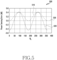
- FIG. 5 is another example of a graph illustrating a power sensing error depending on an impedance change of an antenna according to an embodiment of the disclosure.
- a horizontal axis of a graph 500 means a phase (e.g., unit: degree, °) of antenna impedance, and a vertical axis of the graph 500 means a power sensing error (e.g., unit: decibel, dB).
- a VSWR is 1.925.
- the graph 500 shows a seventh line 510 indicating an error of power based on the voltage peak value of the third line 380 in the graph of FIG. 3C , an eighth line 520 indicating an error of power calculated by multiplying the voltage peak values of the first line 371 and second line 372 in the graph of FIG. 3C , and a ninth line 530 indicating the error of power based on the voltage peak value of the fourth line 390 in the graph of FIG. 3C .
- the seventh line 510 of the graph 500 may be understood as the same as the fifth line 410 of the graph 400 of FIG. 3 .
- the ninth line 530 of the graph 500 may be understood as the same as the sixth line 430 of the graph 400 of FIG. 4 .
- the description on the fifth line 410 and sixth line 430 of FIG. 4 may be equally applied to the seventh line 510 and ninth line 530 of FIG. 5 .
- a power sensing error may change depending on a change in a phase of antenna impedance. For example, when the phase of antenna impedance is 0°, a power sensing error value may be about -0.44dB. When the phase of antenna impedance is 180°, the power sensing error value may be about -0.44dB. In addition, when the phase of antenna impedance is about 90°, the power sensing error value may be about 0.412dB.
- a max error of the power sensing error value may be about -0.44dB.
- Max Error denotes a max error of a power sensing error value.
- ⁇ denotes a reflection coefficient.
- the max error value of the power sensing error value may change by the reflection coefficient.
- the max error of the power sensing error value may decrease as the reflection coefficient approaches 0.
- the power sensing error value when the phase of antenna impedance is about 90°, the power sensing error value is similar as about 0.412dB, whereas when the phase of antenna impedance is about 0° or 180°, the power sensing error value may be different by about 0.44dB.
- the seventh line 510 may have a small difference in a power sensing error with respect to the ninth line 530, whereas the eighth line 520 may have a greater different in the power sensing error than the seventh line 510 with respect to the ninth line 530.
- a power sensing error value for a case where power is calculated by using an average value e.g., an arithmetic average
- an average value e.g., an arithmetic average
- a power sensing error value for a case where power is calculated by performing a multiplication operation on the obtained voltages may have a lower error than a power sensing error value for a case where power is calculated by performing a multiplication operation on the obtained voltages, and power may be measured more accurately when power is calculated by using the average value.
- FIG. 6 illustrates an example of a structure of an electronic device according to an embodiment of the disclosure.
- An electronic device 610 of FIG. 6 has a structure of the conventional electronic device, and an electronic device 620 has a structure of an electronic device according to an embodiment of the disclosure.
- the electronic device 610 may include one Power Amplifier (PA) expressed as equivalent resistance and equivalent power, an antenna expressed as equivalent resistance, and a sensor subjected to coupling by a capacitor at one point between the PA and the antenna.
- PA Power Amplifier
- the electronic device 620 may include one PA expressed as equivalent resistance and equivalent power, an antenna expressed as equivalent resistance, a specific-length transmission line connecting between the PA and the antenna, and two sensors.
- the two sensors of the electronic device 620 may sense a signal voltage respectively at one point between the PA and the transmission line and one point between the transmission line and the antenna.
- the two sensors of the electronic device 620 may calculate power by transferring voltage values obtained through sensing to an ADC & Modem (not shown).
- the ADC & Modem may calculate power by using an average value (e.g., an arithmetic average, a geometric average) of obtained voltages.
- the ADC & Modem may calculate power by using a representative value (e.g., a weight for a maximum value, median value, and reference value) of the obtained voltages.
- FIG. 6 illustrates an electronic device only for convenience of description, and an apparatus and method according to an embodiment of the disclosure are not limited thereto. For example, as described above in FIG.
- the electronic device 620 may include a Doherty power amplifier constructed of a plurality of power amplifiers and a transmission line (e.g., a quarter wave transmission line).
- the electronic device 620 may include one or more sensors, and the one or more sensors may sense a signal voltage at a front end and rear end of the transmission line.
- FIG. 7 is a graph illustrating a signal output voltage depending on an output signal of an electronic device according to an embodiment of the disclosure.
- a horizontal axis of the graph means power (unit: dBm) output from an antenna, and a vertical axis of the graph means an output voltage (unit: V) of a signal obtained by a sensor.
- a return loss is 10dB.
- first lines 710 indicating an output voltage of a signal obtained according to power output from the antenna of the electronic device 610 of FIG. 6 and second lines 720 indicating an output voltage of a signal obtained according to power output from the antenna of the electronic device 620 of FIG. 6 are illustrated.
- the first lines 710 may mean an output voltage obtained from a sensor according to output power, when a phase of antenna impedance changes by a specific value.
- a line closest to a y-axis may mean an output voltage when the antenna impedance is R max .
- a line farthest from the y-axis may mean an output voltage when the impedance of the antenna is R min .
- the second lines 720 may mean an output voltage which is an average value (e.g., an arithmetic average) of voltages obtained from a sensor according to output power, when the phase of antenna impedance changes by a specific value.
- a line closets to the y-axis may mean an output voltage when the antenna impedance is R max .
- a line farthest from the y-axis may mean an output voltage when the antenna impedance is R min .
- the output power of the antenna when the output voltage is 0.6V, the output power of the antenna may be from about 1dBm to about 6dBm. That is, as the antenna impedance changes, power output from the antenna may be output differently with a great width even in case of the same output voltage. Unlike this, referring to the second lines 720, the output power of the antenna may be about 3dBm when the output voltage is 0.6V. That is, even if the antenna impedance changes, power output from the antenna may be almost the same in case of the same output voltage.
- the output power when power is calculated through one output voltage obtained by a sensor, the output power may change depending on a change in antenna impedance even in case of the same output voltage.
- the output voltage and the output power when power is calculated through an output voltage which is an average value of output voltages obtained by the sensor, the output voltage and the output power may have a constant relationship. Accordingly, in the case of the conventional structure, power consumed by an RF chain may have a high error with respect to power obtained by a sensor and calculated based on the voltage. However, in case of a structure according to an embodiment of the disclosure, the power consumed by the RF chain may have a low error with respect to power obtained by a sensor and calculated based on the voltage.
- an error of power calculated using the conventional structure may be about 5.5dB.
- an error of power calculated using an apparatus and method according to an embodiment of the disclosure may be about 0.412 dB.
- an apparatus and method for calculating power based on a voltage of a front end and rear end of a transmission line in a sensing structure based on a quarter wave transmission line provide a more accurate measurement result than calculating of power based on a voltage at one point between the exiting power amplifier and an antenna. Since it is possible to minimize an error between power to be calculated and power to be output even if the antenna impedance changes, a method of calculating power based on the voltage of the front end and rear end of the transmission line may provide a more practical result compared to the existing method of calculating power based on the voltage only at one end.
- a size of an electronic device may be increased due to a measurement device disposed to the electronic device, and a loss may occur due to the measurement device itself. Therefore, power shall be measured indirectly through a voltage.
- a voltage obtained by a sensor may change due to antenna impedance even in case of the same output, calculating of power by using one voltage may result in a high error with respect to power to be output in practice.
- an apparatus and method according to an embodiment of the disclosure calculate power based on voltages of a front end and rear end of a transmission line by using a transmission line (e.g., a quarter wave transmission line) disposed between a power amplifier and an antenna or a transmission line existing inside a power amplifier (e.g., a Doherty power amplifier), an error with respect to power to be output in practice may be low despite a change in antenna impedance.
- a transmission line e.g., a quarter wave transmission line
- a transmission line existing inside a power amplifier e.g., a Doherty power amplifier
- a transmission line existing inside a power amplifier (e.g., a Doherty power amplifier) is used for the aforementioned power measurement, power consumption may be minimized.
- a power amplifier e.g., a Doherty power amplifier
- accuracy may be higher than a case where power is measured indirectly.
- it is inefficient since a size of the electronic device may be increased due to a device for performing direct measurement, and power may be consumed by the device.
- an apparatus and method for calculating power through the sensing structure based on the quarter wave transmission line may secure accuracy similar to a method of directly measuring power, since power is calculated and a plurality of voltages are measured by using a transmission line inside a Doherty power amplifier.
- a separate measurement device is not additionally required, it may also be efficient in terms of power consumption.
- an apparatus and method according to an embodiment of the disclosure may provide a more efficient result than a case of using a signal of a mmWave band. For example, assuming that a return loss of an antenna is 10dB as described above, an error of power calculated in one RF chain according to the conventional structure may be about 6dB. In this case, if the signal of the mmWave band is used, a plurality of RF chains may be included in the electronic device. Accordingly, when the electronic device uses the signa of the mmWave band, an error between power to be calculated and power consumed in practice may be high. In order to minimize an influence used by the high error, the sensing structure based on the quarter wave transmission line according to an embodiment of the disclosure may be used.
- An electronic device which transmits a signal of a mmWave band may require accurate power measurement for efficient power distribution.
- the signal of the mmWave band may change sensitively due to various factors.
- power calculation through a sensing structure based on a quarter wave transmission line may be predicted (calculated) similarly to power consumed in practice in the electronic device.
- an error between power to be calculated and power consumed in practice may be low (e.g., about 0.412dB). Accordingly, power distribution may be achieved efficiently.
- a method of measuring power of a signal may include obtaining, by at least one sensor, a first voltage of the signal at a first point between a power amplifier and a transmission line, obtaining, by the at least one sensor, a second voltage of the signal at a second point between the transmission line and an antenna, and calculating power, based on the first voltage and the second voltage.
- a length of the transmission line may be associated with a wavelength of the signal.
- the length of the transmission line may be a quarter of the wavelength of the signal.
- the power amplifier may be a Doherty power amplifier.
- the transmission line may be a transmission line having a length which is a quarter of the wavelength of the signal existing inside the Doherty power amplifier.
- a phase difference between the first phase and the second phase may be about 180°.
- the calculating of the power may be based on an average value of the first voltage and the second voltage.
- the average value may be an arithmetic average value of the first voltage and the second voltage.
- the calculating of the power may be based on at least one of a maximum value, median value, or weight of the first voltage and the second voltage.
- An electronic device of a wireless communication system may include a power amplifier, an antenna, a transmission line, at least one sensor, and at least one processor electrically coupled to the at least one sensor.
- the at least one sensor may be configured to obtain a first voltage of a signal at a first point between the power amplifier and the transmission line, and obtain a second voltage of the signal at a second point between the transmission line and the antenna.
- the at least one processor may be configured to calculate power, based on the first voltage and second voltage obtained by the at least one sensor.
- a length of the transmission line may be associated with a wavelength of the signal.
- the length of the transmission line may be a quarter of the wavelength of the signal.
- the power amplifier may be a Doherty power amplifier.
- the transmission line may be a transmission line having a length which is a quarter of the wavelength of the signal existing inside the Doherty power amplifier.
- a second phase of a second voltage which is a voltage of the second point may have a phase difference of about 180° with respect to the first phase.
- the at least one processor may be configured to calculate the power, based on an average value of the first voltage and the second voltage.
- At least part of the support member is constructed of a metal material, and the average value may be an arithmetic average value of the first voltage and the second voltage.
- the at least one processor may be configured to calculate the power, based on at least one of a maximum value, median value, or weight of the first voltage and the second voltage.
- An electronic device of a wireless communication system may include a plurality of RF chains, a plurality of antennas corresponding to the plurality of RF chains, a transmission line, at least one sensor, and at least one processor electrically coupled to the at least one sensor.
- at least one RF chain may include a power amplifier.
- the at least one sensor may be configured to obtain a first voltage of a signal at a first point between the power amplifier and the transmission line, and obtain a second voltage of the signal at a second point between the at least one antenna among the plurality of antennas and the transmission line.
- the at least one processor may be configured to calculate power, based on the first voltage and second voltage obtained by the at least one sensor.
- a length of the transmission line may be associated with a wavelength of the signal.
- the length of the transmission line may be a quarter of the wavelength of the signal.
- the power amplifier may be a Doherty power amplifier.
- the transmission line may be a transmission line having a length which is a quarter of the wavelength of the signal existing inside the Doherty power amplifier.
- a second phase of a second voltage which is a voltage of the second point may have a phase difference of about 180° with respect to the first phase.
- the at least one processor may be configured to calculate the power, based on an average value of the first voltage and the second voltage.
- the at least one processor may be configured to calculate the power, based on at least one of a maximum value, median value, or weight of the first voltage and the second voltage.
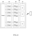
- FIG. 8 illustrates a functional configuration of an electronic device according to various embodiments of the disclosure.
- An electronic device 810 may mean the electronic device 100 of FIG. 1 or the electronic device 200 of FIG. 2 .
- the electronic device 810 may be an electronic device using a signal of a mmWave band.
- a specific-length transmission line e.g., a quarter wave transmission line
- a specific length-transmission line e.g., a quarter wave transmission line
- the electronic device 810 may include an antenna unit 811, a filter unit 812, a Radio Frequency (RF) processing unit 813, and a control unit 814.
- RF Radio Frequency
- the antenna unit 811 may include a plurality of antennas.
- the antenna performs functions for transmitting and receiving signals through a radio channel.
- the antenna may include a radiator formed on a substrate (e.g., a PCB).
- the antenna may radiate an upconverted signal on the radio channel or obtain a signal radiated by another device.
- Each antenna may be referred to as an antenna element or an antenna device.
- the antenna unit 811 may include an antenna array in which a plurality of antenna elements constitute an array.
- the antenna unit 811 may be electrically coupled to the filter unit 812 through RF signal lines.
- the antenna unit 811 may be mounted on a PCB including a plurality of antenna elements.
- the PCB may include a plurality of RF signal lines to couple each antenna element and a filter of the filter unit 812.
- the RF signal lines may be referred to as a feeding network.
- the antenna unit 811 may provide a received signal to the filter unit 812 or may radiate the signal provided from the filter unit 812 into the air.
- An antenna of the structure according to an embodiment of the disclosure may be included in the antenna unit 811,
- the antenna unit 811 may include at least one antenna module having a dual-polarized antenna.
- the dual-polarized antenna may be, for example, a cross-pol (x-pol) antenna.
- the dual-polarized antenna may include two antenna elements corresponding to different polarizations.
- the dual-polarized antenna may include a first antenna element having a polarization of +45° and a second antenna element having a polarization of -45°. It is obvious that the polarization may be formed of other polarizations orthogonal to each other, in addition to +45° and -45°.
- Each antenna element may be coupled to a feeding line, and may be electrically coupled to the filter unit 812, the RF processing unit 813, and the control unit 814 to be described below.
- the dual-polarized antenna may be a patch antenna (or a micro-strip antenna). Since the dual-polarized antenna has a form of a patch antenna, it may be easily implemented and integrated as an array antenna. Two signals having different polarizations may be input to respective antenna ports. Each antenna port corresponds to an antenna element. For high efficiency, it is required to optimize a relationship between a co-pol characteristic and a cross-pol characteristic between the two signals having the different polarizations.
- the co-pol characteristic indicates a characteristic for a specific polarization component and the cross-pol characteristic indicates a characteristic for a polarization component different from the specific polarization component.
- the filter unit 812 may perform filtering to transmit a signal of a desired frequency.
- the filter unit 812 may perform a function for selectively identifying a frequency by forming a resonance.
- the filter unit 812 may structurally form the resonance through a cavity including a dielectric.
- the filter unit 812 may form a resonance through elements which form inductance or capacitance.
- the filter unit 812 may include a Bulk Acoustic Wave (BAW) filter or a Surface Acoustic Wave (SAW) filter.
- BAW Bulk Acoustic Wave
- SAW Surface Acoustic Wave
- the filter unit 812 may include at least one of a band pass filter, a low pass filter, a high pass filter, and a band reject filter.
- the filter unit 812 may include RF circuits for obtaining a signal of a frequency band for transmission or a frequency band for reception.
- the filter unit 812 may electrically couple the antenna unit 811 and the RF processing unit 813 to each other.
- the RF processing unit 813 may include a plurality of RF paths.
- the RF path may be a unit of a path through which a signal received through an antenna or a signal radiated through the antenna passes. At least one RF path may be referred to as an RF chain.
- the RF chain may include a plurality of RF elements.
- the RF elements may include an amplifier, a mixer, an oscillator, a Digital-to-Analog Converter (DAC), an Analog-to-Digital Converter (ADC), or the like.
- the RF processing unit 813 may include an up converter which up-converts a digital transmission signal of a baseband to a transmission frequency, and a DAC which converts the converted digital transmission signal into an analog RF transmission signal.
- the converter and the DAC constitute a transmission path in part.
- the transmission path may further include a Power Amplifier (PA) or a coupler (or a combiner).
- PA Power Amplifier
- the RF processing unit 813 may include an ADC which converts an analog RF reception signal into a digital reception signal and a down converter which converts the digital reception signal into a digital reception signal of a baseband.
- the ADC and the down converter constitute a reception path in part.
- the reception path may further include a Low-Noise Amplifier (LNA) or a coupler (or a divider).
- LNA Low-Noise Amplifier
- RF parts of the RF processing unit may be implemented on a PCB.
- the antennas and the RF parts of the RF processing unit may be implemented on the PCB, and filters may be repeatedly fastened between one PCB and another PCB to constitute a plurality of layers.
- a power amplifier and sensor having a structure according to an embodiment of the disclosure may be included in the RF processing unit 813 of FIG. 8 . That is, the RF processing unit 813 may be understood as part of the RF chain of the disclosure.
- a specific-length transmission line having a structure according to an embodiment of the disclosure may exist inside a specific power amplifier (e.g., a Doherty power amplifier), and thus may be included in the RF processing unit 813.
- the disclosure is not limited thereto, and the specific-length transmission line may be disposed to a region which connects the RF processing unit 813 and the antenna unit 811.
- a length of the transmission line may be associated with a wavelength of a signal passing through the transmission line.
- the control unit 814 may provide overall control to the electronic device 810.
- the control unit 814 may include various modules for performing communication.
- the control unit 814 may include at least one processor such as a modem.
- the control unit 814 may include modules for digital signal processing.
- the control unit 814 may include a modem.
- the control unit 814 In data transmission, the control unit 814 generates complex symbols by encoding and modulating a transmission bit-stream.
- the control unit 814 restores a reception bit-stream by demodulating and decoding a baseband signal.
- the control unit 814 may perform functions of a protocol stack required in a communication standard.
- An ADC & Modem having a structure according to an embodiment of the disclosure may be included in the control unit 814 of FIG. 8 .
- the functional configuration of the electronic device 810 is described in FIG. 8 as a device capable of utilizing an apparatus and method according to various embodiments.
- the example of FIG. 8 is only an exemplary configuration for utilizing the apparatus and method according to various embodiments of the disclosure described with reference to FIG. 1 to FIG. 7 , and embodiments of the disclosure are not limited to components of the device of FIG. 8 . Therefore, in an electronic device including a specific-length transmission line between a power amplifier and an antenna or including a specific-length transmission line inside the power amplifier, a method of measuring power based on voltages of a front end and rear end of the transmission line, an apparatus using the method, or an electronic device including the apparatus using the method may also be understood as an embodiment of the disclosure.
- the disclosure is not limited to the structure illustrated in FIG. 1 to FIG. 7 .
- the power may also be calculated based on a representative value of voltages measured in another portion (e.g., a third connection portion, a fourth connection portion, etc.).
- the electronic device may include a plurality of power amplifiers, a plurality of specific-length transmission lines, or a plurality of sensors.
- computer readable recording medium for storing one or more programs (i.e., software modules) may be provided.
- the one or more programs stored in the computer readable recording medium are configured for execution performed by one or more processors in the electronic device.
- the one or more programs include instructions for allowing the electronic device to execute the methods based on the embodiments disclosed in the claims and/or specification of the disclosure.
- the program (i.e., the software module or software) may be stored in a random access memory, a non-volatile memory including a flash memory, a read only memory (ROM), an electrically erasable programmable read only memory (EEPROM), a magnetic disc storage device, a compact disc-ROM (CD-ROM), digital versatile discs (DVDs) or other forms of optical storage devices, and a magnetic cassette.
- a non-volatile memory including a flash memory, a read only memory (ROM), an electrically erasable programmable read only memory (EEPROM), a magnetic disc storage device, a compact disc-ROM (CD-ROM), digital versatile discs (DVDs) or other forms of optical storage devices, and a magnetic cassette.
- the program may be stored in a memory configured in combination of all or some of these storage media.
- the configured memory may be plural in number.
- the program may be stored in an attachable storage device capable of accessing the electronic device through a communication network such as the Internet, an Intranet, a local area network (LAN), a wide LAN (WLAN), or a storage area network (SAN) or a communication network configured by combining the networks.
- the storage device may have access to a device for performing an embodiment of the disclosure via an external port.
- an additional storage device on a communication network may have access to the device for performing the embodiment of the disclosure.
- a component included in the disclosure is expressed in a singular or plural form according to the specific embodiment proposed herein.
- the singular or plural expression is selected properly for a situation proposed for the convenience of explanation, and thus the various embodiments of the disclosure are not limited to a single or a plurality of components. Therefore, a component expressed in a plural form may also be expressed in a singular form, or vice versa.
Landscapes
- Physics & Mathematics (AREA)
- General Physics & Mathematics (AREA)
- Engineering & Computer Science (AREA)
- Power Engineering (AREA)
- Electromagnetism (AREA)
- Transmitters (AREA)
- Amplifiers (AREA)
Abstract
Description
- The disclosure relates, in general, to a wireless communication system, and in particular, to a method and apparatus for measuring strength of a signal in the wireless communication system.
- To meet a demand on wireless data traffic which has been in an increasing trend after a 4th Generation (4G) communication system was commercialized, there is an ongoing effort to develop an improved 5th Generation (5G) communication system or a pre-5G communication system. For this reason, the 5G communication system or the pre-5G communication system is called a beyond 4G network communication system or a post Long Term Evolution (LTE) system.
- To achieve a high data transfer rate, the 5G communication system is considered to be implemented in an ultra-high frequency band. To reduce a propagation path loss at the ultra-high frequency band and to increase a propagation delivery distance, beamforming, massive Multiple Input Multiple Output (MIMO), full dimensional MIMO (FD-MIMO), array antenna, analog beam-forming, and large scale antenna techniques are under discussion in the 5G communication system.
- In addition, to improve a network of a system, techniques such as an evolved small cell, an advanced small cell, a cloud Radio Access Network (RAN), an ultra-dense network, Device to Device (D2D) communication, a wireless backhaul, a moving network, cooperative communication, Coordinated Multi-Points (CoMP), and reception interference cancellation, or the like are being developed in the 5G communication system.
- In addition thereto, hybrid Frequency shift keying and Quadrature Amplitude Modulation (FQAM) and Sliding Window Superposition Coding (SWSC) as an Advanced Coding Modulation (ACM) technique and Filter Bank Multi Carrier (FBMC), Non Orthogonal Multiple Access (NOMA), and Sparse Code Multiple Access (SCMA), or the like as an advanced access technology are being developed in the 5G system.
- A beamforming technique may be used when using a signal of a millimeter wave (mmWave) band in the wireless communication system. An electronic device performing beamforming may require a plurality of antenna elements, and may require a plurality of Radio Frequency (RF) chains as paths through which signals transmitted or received by the plurality of antenna elements pass. In this case, in order to use the plurality of antenna elements and the plurality of RF chains, the electronic device may need to minimize power consumption. Accordingly, in order to measure power consumed by the signals transmitted or received by the plurality of antenna elements through the plurality of RF chains, there is a need to measure power consumption for each RF chain. However, even if power consumed in the RF chain due to signal transmission or reception is identical, a change in impedance of an antenna for transmitting or receiving the signal may cause a change in a voltage of the signal. That is, it may be inaccurate to measure the power consumed in the RF change through the voltage of the signal passing through the RF chain. Accordingly, in order to minimize an error of power measurement, it is required to measure signal strength in a more effective manner by considering the signal voltage which changes depending on the change in the antenna impedance.
- Based on the aforementioned discussion, the disclosure provides a method and apparatus in which a transmission line having a specific length is used to accurately measure power of a signal passing through the transmission line in a wireless communication system.
- In addition, the disclosure provides a structure capable of accurately measuring signal power by arranging a transmission line without having to use an additional device in the wireless communication system.
- According to various embodiments of the disclosure, a method of measuring power of a signal may include obtaining, by at least one sensor, a first voltage of the signal at a first point between a power amplifier and a transmission line, obtaining, by the at least one sensor, a second voltage of the signal at a second point between the transmission line and an antenna, and calculating power, based on the first voltage and the second voltage. A length of the transmission line may be associated with a wavelength of the signal.
- According to various embodiments of the disclosure, an electronic device of a wireless communication system may include a power amplifier, an antenna, a transmission line, at least one sensor, and at least one processor electrically coupled to the at least one sensor. The at least one sensor may be configured to obtain a first voltage of a signal at a first point between the power amplifier and the transmission line, and obtain a second voltage of the signal at a second point between the transmission line and the antenna. The at least one processor may be configured to calculate power, based on the first voltage and second voltage obtained by the at least one sensor. A length of the transmission line may be associated with a wavelength of the signal.
- According to various embodiments of the disclosure, an electronic device of a wireless communication system may include a plurality of Radio Frequency (RF) chains, a plurality of antennas corresponding to the plurality of RF chains, a transmission line, at least one sensor, and at least one processor electrically coupled to the at least one sensor. Among the plurality of RF chains, at least one RF chain may include a power amplifier. The transmission line may be disposed between the power amplifier and at least one antenna corresponding to the power amplifier. The at least one sensor may be configured to obtain a first voltage of a signal at a first point between the power amplifier and the transmission line, and obtain a second voltage of the signal at a second point between the at least one antenna and the transmission line. The at least one processor may be configured to calculate power, based on the first voltage and second voltage obtained by the at least one sensor. A length of the transmission line may be associated with a wavelength of the signal.
- An apparatus and method according to various embodiments of the disclosure measure voltages of a signal passing through a specific-length transmission line disposed between a power amplifier and an antenna, thereby accurately calculating power irrespective of a change in antenna impedance.
- An apparatus and method according to various embodiments of the disclosure use a specific power amplifier, thereby accurately calculating power without having to dispose an additional transmission line.
- In addition thereto, advantages acquired in the disclosure are not limited to the aforementioned advantages, and other advantages not mentioned herein may be clearly understood by those skilled in the art to which the disclosure pertains from the following descriptions.
-
-
FIG. 1 illustrates an example of an electronic device according to an embodiment of the disclosure; -
FIG. 2 illustrates an example of an electronic device including a Doherty power amplifier according to an embodiment of the disclosure; -
FIG. 3A illustrates an example of a circuit diagram of an electronic device according to an embodiment of the disclosure; -
FIG. 3B illustrates an example of a smith chart representing impedance of an antenna according to an embodiment of the disclosure; -
FIG. 3C is an example of a graph illustrating a voltage peak depending on an impedance change of an antenna according to an embodiment of the disclosure; -
FIG. 4 is an example of a graph illustrating a power sensing error depending on an impedance change of an antenna according to an embodiment of the disclosure; -
FIG. 5 is another example of a graph illustrating a power sensing error depending on an impedance change of an antenna according to an embodiment of the disclosure; -
FIG. 6 illustrates an example of a structure of an electronic device according to an embodiment of the disclosure; -
FIG. 7 is a graph illustrating an output voltage depending on an output signal of an electronic device according to an embodiment of the disclosure; and -
FIG. 8 illustrates a functional configuration of an electronic device according to various embodiments of the disclosure. - With regard to the description of the drawings, the same or similar reference numerals may be used to refer to the same or similar elements.
- Terms used in the disclosure are for the purpose of describing particular embodiments only and are not intended to limit other embodiments. A singular expression may include a plural expression unless there is a contextually distinctive difference. All terms (including technical and scientific terms) used herein have the same meaning as commonly understood by those ordinarily skilled in the art disclosed in the disclosure. It will be further understood that terms, such as those defined in commonly used dictionaries, should be interpreted as having a meaning that is consistent with their meaning in the context of the relevant art, and will not be interpreted in an idealized or overly formal sense unless expressly so defined herein. Optionally, the terms defined in the disclosure should not be interpreted to exclude the embodiments of the disclosure.
- A hardware-based approach is described for example in the various embodiments of the disclosure described hereinafter. However, since the various embodiments of the disclosure include a technique in which hardware and software are both used, a softwarebased approach is not excluded in the embodiments of the disclosure.
- Hereinafter, terms used to refer to parts of an electronic device (e.g., a board structure, a substrate, a Printed Circuit Board (PCB), a Flexible PCB (FPCB), a module, an antenna, an antenna element, a circuit, a processor, a chip, a component, and a device), terms used to refer to a shape of the parts (e.g., a construction body, a construction object, a support portion, a contact portion, a protrusion, and an opening), terms used to refer to a connection portion between the construction bodies (e.g., a connection line, a feeding line, a connection portion, a contact portion, a support portion, a contact construction body, a conductive member, an assembly), terms used to refer to a circuitry (e.g., a PCB, an FPCB, a signal line, a feeding line, a data line, an RF signal line, an antenna line, an RF path, an RF module, and an RF circuit), and the like are exemplified for convenience of explanation. Therefore, the disclosure is not limited to terms described below, and thus other terms having the same technical meaning may also be used. In addition, the term "... unit', '... device', '...member', '...body', or the like may imply at least one configuration or may imply a unit of processing a function.
- Conventionally, in an electronic device including a plurality of RF chains, a sensor disposed to an Integrated Circuit (IC) inside the RF chain has been used to measure power of a signal transmitted from an antenna. The power is calculated indirectly through a signal voltage measured through the sensor. However, since the voltage and power of the signal have a constant relationship only when the antenna has constant impedance, the impedance of the antenna may be changed in practice due to an external factor (e.g., an arrangement of an adjacent circuit) or the like, and thus it may be inaccurate to measure the signal power by using only the signal voltage.
- Hereinafter, the disclosure proposes a structure for accurately measuring power of a signal passing through an RF chain even in an environment in which impedance of an antenna changes. A transmission line having a specific length is disposed between the antenna and a power amplifier disposed on the RF chain, and a sensor obtains voltages of signals at front and rear end of the transmission line having the specific length. Therefore, the electronic device may more accurately measure power of the signal, based on the obtained voltages.
-
FIG. 1 illustrates an example of an electronic device according to an embodiment of the disclosure. Although an electronic device including one power amplifier, one antenna, one transmission line coupling the power amplifier and the antenna, one sensor, and one Analog to Digital Converter (ADC) & Modulation and demodulation (Modem) is illustrated inFIG. 1 for convenience of description, the disclosure is not limited thereto. For example, in the electronic device, the power amplifier and the antenna may be coupled by a plurality of transmission lines. As another example, the electronic device may include a plurality of power amplifiers, as described below with reference toFIG. 2 . As another example, the plurality of sensors may be coupled to the transmission line. - Referring to
FIG. 1 , anelectronic device 100 may include a Power Amplifier (PA) 110, a Transmission Line (T/L) 120, anantenna 140, asensor 150, an Analog to digital Converter & Modulation and demodulation (ADC & Modem) 160. According to an embodiment, thePA 110 may be disposed on a plurality of RF chains in theelectronic device 100 including the plurality of RF chains, as described below with reference toFIG. 8 . According to an embodiment, thePA 110 may be disposed on at least one RF chain among the plurality of RF chains. For example, thePA 110 may be disposed only on one RF chain among the plurality of RF chains. As another example, thePA 110 may be disposed only on some adjacent RF chains among the plurality of RF chains. As another example, thePA 110 may be disposed only any RF chains among the plurality of RF chains. - According to an embodiment, the
PA 110 may be coupled to thetransmission line 120. For example, thePA 110 may be coupled to one end of thetransmission line 120 only at any one portion referred to as afirst connection portion 131. According to another embodiment, although not shown inFIG. 1 , thePA 110 may be coupled to the plurality oftransmission lines 120. For example, thePA 110 may be coupled to two ormore transmission lines 120. - According to an embodiment, the
PA 110 may be constructed of a plurality of power amplifiers. For example, as described below with reference toFIG. 2 , thePA 110 may be constructed of a Doherty power amplifier including two power amplifiers. - According to an embodiment, one end of the
transmission line 120 may be coupled to an output stage of thePA 110, and the other end of thetransmission line 120 may be coupled to theantenna 140. According to an embodiment, any one portion between thetransmission line 120 and the output stage of thePA 110 may be referred to as thefirst connection portion 131, and any one portion between thetransmission line 120 and theantenna 140 may be referred to as asecond connection portion 132. According to an embodiment, thetransmission line 120 may be a path for transmitting to the antenna 140 a signal output from the output stage of thePA 110. In addition, according to an embodiment, thetransmission line 120 may be included inside thePA 110. For example, as described below with reference toFIG. 2 , thetransmission line 120 may be a specific-length transmission line (e.g., a quarter wave transmission line) existing inside the Doherty power amplifier. - According to an embodiment, the length of the
transmission line 120 may be associated with a wavelength of a signal output from the output stage of thePA 110. For example, when the wavelength of the signal output from thePA 110 is λ, the length of thetransmission line 120 may be λ/4. However, the disclosure is not limited thereto, and the length of thetransmission line 120 may vary when configuring theelectronic device 100. For example, the length of thetransmission line 120 may be shorter than λ/4. As another example, the length of thetransmission line 120 may be longer than λ/4. That is, it may mean that the length of thetransmission line 120 may change by considering a design restriction of an antenna and signal or an influence of adjacent elements, when configuring theelectronic device 100, - According to another embodiment, the
transmission line 120 may be constructed of a lumped circuit. In other words, the transmission line may be replaced through an equivalent lumped circuit constructed to have the same impedance as that of thetransmission line 120. For example, in order to construct the lumped circuit equivalent to thetransmission line 120, the equivalent lumped circuit may be constructed by combining a capacitor and an inductor. - According to an embodiment, the
antenna 140 may be constructed by at least one antenna element. For example, theelectronic device 100 using a signal of a millimeter wave (mmWave) band may include a plurality of antenna elements to perform beamforming. In this case, one sub-array may be constructed by some antenna elements among the plurality of antenna elements. Although oneantenna 140 is illustrated inFIG. 1 for convenience of description, the disclosure is not limited thereto, and it may mean that thetransmission line 120 is coupled to a node to be coupled to the plurality of antenna elements. - According to an embodiment, the
sensor 150 may be electrically coupled at thefirst connection portion 131 which is a portion between thetransmission line 120 and thePA 110. In addition, thesensor 150 may be electrically coupled at thesecond connection portion 132 which is a portion between thetransmission line 120 and theantenna 140. According to an embodiment, thesensor 150 may measure a voltage value of a signal transmitted from each of thefirst connection portion 131 and thesecond connection portion 132. For example, when a voltage at thefirst connection portion 131 of the signal to be transmitted is a first voltage and a voltage at thesecond connection portion 132 is a second voltage, the sensor may measure values of the first voltage and second voltage. In this case, the value of the first voltage and the value of the second voltage of the signal measured by thesensor 150 may mean a peak value of the voltage. According to another embodiment, a plurality of voltage values at thefirst connection portion 131 of the signal to be transmitted and a plurality of voltage values at thesecond connection portion 132 may be measured. For example, a value expressed by a representative value (e.g., an average value, a maximum value, etc.) by measuring voltages of points (e.g., 3 points) adjacent to thefirst connection portion 131 may mean the first voltage. As another example, a value expressed by a representative value of voltages measured by measuring a voltage for each specific period at thefirst connection portion 131 may mean the first voltage. In the disclosure, the measuring of the voltage may be understood as obtaining a value of the voltage. - According to an embodiment, the
sensor 150 may transmit the obtained signal voltage values to the ADC &Modem 160. In detail, thesensor 150 may transmit voltage values obtained from thefirst connection portion 131 and thesecond connection portion 132 to the Modem by digitalizing signal voltage values obtained through the ADC. - According to an embodiment, the ADC &
Modem 160 may calculate signal power by using the obtained signal voltage values. In other words, a value obtained by digitalizing signal voltage values obtained through thesensor 150 may be transferred to the Modem through the ADC to convert (or calculate) the obtained signal voltage values into power. According to an embodiment, the ADC &Modem 160 may calculate power by using an average value of the obtained signal voltage values. For example, when a value of the first voltage is denoted by V1 and a value of the second voltage is denoted by V2, the ADC &Modem 160 may calculate power through (V1+V2)/2 which is an arithmetic average of the values of the first voltage and second voltage. As another example, the ADC &Modem 160 may calculate power through a geometric average (e.g.,
Modem 160 may calculate signal power, based on at least one of a maximum value, a median value, and a weight for a specific value of the first voltage and second voltage values. For example, when a first weight for the first voltage is denoted by wi and a second weight for the second voltage is denoted by w2, the ADC &Modem 160 may calculate power through a voltage V=w1V1+w2V2 (where w1+w2=1) depending on weights of the first voltage and second voltage values. - As described above, the
electronic device 100 may be constructed to include thetransmission line 120 between thePA 110 and theantenna 140, and thesensor 150 of theelectronic device 100 may measure signal voltage values at thefirst connection portion 131 and thesecond connection portion 132. In addition, the ADC &Modem 160 may convert the signal voltage values obtained by thesensor 150 into an average value or the like to calculate power of a signal transmitted by theantenna 140. - Hereinafter, a structure of an electronic device using a Doherty power amplifier instead of the power amplifier and transmission line of
FIG. 1 will be described with reference toFIG. 2 . -
FIG. 2 illustrates an example of an electronic device including a Doherty power amplifier according to an embodiment of the disclosure. Although an electronic device including one Doherty power amplifier, one antenna, one sensor, and one ADC & Modem is illustrated inFIG. 2 for convenience of description, the disclosure is not limited thereto. For example, the electronic device may include a plurality of antennas coupled by means of a single node, and the single node may be coupled to an output stage of the Doherty power amplifier. As another example, a plurality of sensors may be coupled to a transmission line. - Referring to
FIG. 2 , anelectronic device 200 may include aDoherty power amplifier 210, anantenna 240, asensor 250, and an ADC &Modem 260. According to an embodiment, theDoherty power amplifier 210 may be disposed on a plurality of RF chains in theelectronic device 200 including the plurality of RF chains, as described below with reference toFIG. 8 . According to another embodiment, theDoherty power amplifier 210 may be disposed on at least one RF chain among the plurality of RF chains. For example, theDoherty power amplifier 210 may be disposed only on one RF chain among the plurality of RF chains. As another example, thepower amplifier 210 may be disposed only on some adjacent RF chains among the plurality of RF chains. As another example, theDoherty power amplifier 210 may be disposed only any RF chains among the plurality of RF chains. - According to an embodiment, the
Doherty power amplifier 210 may be coupled to onemain power amplifier 211, onepeak power amplifier 212, and at least onetransmission line 220 coupling themain power amplifier 211 and thepeak power amplifier 212. Thetransmission line 220 coupling themain power amplifier 211 and thepeak power amplifier 212 is assumed as onetransmission 220 inFIG. 2 only for convenience of description, and the disclosure is not limited thereto. For example, a transmission line for signal distribution may also be disposed at respective input stages of themain power amplifier 211 and thepeak power amplifier 212. In other words, thetransmission line 220 ofFIG. 2 means a transmission line existing inside theDoherty power amplifier 210, and it may not mean that an additional transmission line is disposed to theelectronic device 200. Therefore, thetransmission line 120 ofFIG. 1 and thetransmission line 220 ofFIG. 2 may not mean the same transmission signal. - According to an embodiment, one end of the
transmission line 220 may be coupled to an output stage of themain power amplifier 211, and another end of thetransmission line 220 may be coupled to thepeak power amplifier 212 and theantenna 240. For example, any one portion between thetransmission line 220 and themain power amplifier 211 may be referred to as afirst connection portion 231. As another example, any one portion between thetransmission line 220 and thepeak power amplifier 212 or between thetransmission line 220 and theantenna 240 may be referred to as asecond connection portion 232. Although any one portion between thetransmission line 220 and theantenna 240 is illustrated inFIG. 2 as thesecond connection portion 232, even if any one portion between thetransmission line 220 and thepeak power amplifier 212 serves as thesecond connection portion 232, it is electrically the same node in practice and thus may be understood to be the same. According to an embodiment, thetransmission line 220 may be disposed inside theDoherty power amplifier 210, which may be a path for transmitting signals output from an output stage of each power amplifier inside theDoherty power amplifier 210 to theantenna 240. - According to an embodiment, a length of the
transmission line 220 may be associated with a wavelength of signals output from the output stages of themain power amplifier 211 andpeak power amplifier 212 of theDoherty power amplifier 210. For example, when the wavelength of the signal output from theDoherty power amplifier 210 is denoted by λ, the length of thetransmission line 220 may be λ/4. - According to an embodiment, the
antenna 240 may be constructed by at least one antenna element. For example, theelectronic device 200 using a signal of a mmWave band may include a plurality of antenna elements to perform beamforming. In this case, one sub-array may be constructed by some antenna elements among the plurality of antenna elements. Although oneantenna 240 is illustrated inFIG. 1 for convenience of description, the disclosure is not limited thereto, and it may mean that thetransmission line 220 is coupled to a node to be coupled to the plurality of antenna elements. - According to an embodiment, the
sensor 250 may be electrically coupled at thefirst connection portion 231 which is a portion between thetransmission line 220 and themain amplifier 211 of theDoherty power amplifier 210. In addition, thesensor 250 may be electrically coupled at thesecond connection portion 232 which is a portion between thetransmission line 220 and theantenna 240 or between thetransmission line 220 and thepeak power amplifier 212. According to an embodiment, thesensor 250 may measure a voltage value of a signal transmitted from each of thefirst connection portion 231 and thesecond connection portion 232. For example, when a voltage at thefirst connection portion 231 of the signal to be transmitted is a first voltage and a voltage at thesecond connection portion 232 is a second voltage, the sensor may measure values of the first voltage and second voltage. In this case, the value of the first voltage and the value of the second voltage of the signal measured by thesensor 250 may mean a peak value of the voltage. According to another embodiment, a plurality of voltage values at thefirst connection portion 231 of the signal to be transmitted and a plurality of voltage values at thesecond connection portion 232 may be measured. For example, a value expressed by a representative value (e.g., an average value, a maximum value, etc.) by measuring voltages of points (e.g., 3 points) adjacent to thefirst connection portion 231 may mean the first voltage. As another example, a value expressed by a representative value of voltages measured by measuring a voltage for each specific period at thefirst connection portion 231 may mean the first voltage. In the disclosure, the measuring of the voltage may be understood as obtaining a value of the voltage. - According to an embodiment, the
sensor 250 may transmit the obtained signal voltage values to the ADC &Modem 260. In detail, thesensor 250 may transmit voltage values obtained from thefirst connection portion 231 and thesecond connection portion 232 to the Modem by digitalizing signal voltage values obtained through the ADC. - According to an embodiment, the ADC &
Modem 260 may calculate signal power by using the obtained signal voltage values. In other words, a value obtained by digitalizing signal voltage values obtained through thesensor 250 may be transferred to the Modem through the ADC to convert (or calculate) the obtained signal voltage values into power. According to an embodiment, the ADC &Modem 260 may calculate power by using an average value of the obtained signal voltage values. For example, when a value of the first voltage is denoted by V1 and a value of the second voltage is denoted by V2, the ADC &Modem 260 may calculate power through (V1+V2)/2 which is an arithmetic average of the values of the first voltage and second voltage. As another example, the ADC &Modem 260 may calculate power through a geometric average (e.g.,
Modem 260 may calculate signal power, based on at least one of a maximum value, a median value, and a weight for a specific value of the first voltage and second voltage values. For example, when a first weight for the first voltage is denoted by wi and a second weight for the second voltage is denoted by w2, the ADC &Modem 260 may calculate power through a voltage V=w1V1+w2V2 (where w1+w2=1) depending on weights of the first voltage and second voltage values. - As described above, the
electronic device 200 may be constructed to include theDoherty power amplifier 210 and theantenna 240, and thesensor 250 of theelectronic device 200 may measure signal voltage values at thefirst connection portion 231 and thesecond connection portion 232. In addition, the ADC &Modem 260 may convert the signal voltage values obtained by thesensor 250 into an average value or the like to calculate power of a signal transmitted by theantenna 240. - A voltage of a signal has conventionally been measured at one point between a power amplifier and an antenna to calculate power of the signal, which may result in a change in impedance of the antenna. Accordingly, since a relationship between the voltage and the power may not be constant, an error may occur when measuring the power of the signal. Therefore, a structure of being electrically coupled to the sensor to measure a voltage at front and rear ends of a transmission line having a specific length according to an embodiment of the disclosure (hereinafter, a sensing structure based on a quarter wave transmission line) may be used to calculate power through a representative value (e.g., an average value, a median value, a weight, a maximum value, etc.) of voltages obtained at the front and rear ends of the transmission line, thereby minimizing an error of power calculation. A process for this will be described in detail with reference to
FIG. 3A to FIG. 7 . - Although an example in which power is calculated based on an average value depending on an arithmetic average of voltages measured by a sensor is described hereinafter, the power may also be calculated based on a voltage value calculated by using a geometric average, a weight, or the like as described above.
-
FIG. 3A illustrates an example of a circuit diagram of an electronic device according to an embodiment of the disclosure.FIG. 3B illustrates an example of a smith chart representing impedance of an antenna according to an embodiment of the disclosure. A circuit diagram of anelectronic device 300 which is a simplification of theelectronic device 100 ofFIG. 1 is illustrated for convenience of description inFIG. 3A . Therefore, theelectronic device 300 ofFIG. 3A may be understood as the same as theelectronic device 100 ofFIG. 1 . For example, the description on thePA 110 ofFIG. 1 may be applied to aPA 310 ofFIG. 3 . However,FIG. 3A is only a simplified circuit diagram of theelectronic device 100 ofFIG. 1 for convenience of description, and theelectronic device 300 ofFIG. 3A may be understood as the same as theelectronic device 200 using theDoherty power amplifier 210 ofFIG. 2 . - Referring to
FIG. 3A , theelectronic device 300 may include thePA 310, atransmission line 320, and anantenna 340. ThePA 310 may be replaced with equivalent impedance and power. In addition, theantenna 340 may be replaced with equivalent impedance. According to an embodiment, afirst connection portion 331 may be any portion between thetransmission line 320 and thePA 310, and asecond connection portion 332 may be any portion between thetransmission line 320 and theantenna 340. According to an embodiment, a sensor (not shown) may measure values of a first voltage and second voltage of respective signals at thefirst connection portion 331 and thesecond connection portion 332. The sensor may transmit the values of the first voltage and second voltage of the obtained signal to an ADC & Modem (not shown) of theelectronic device 300, and thus the ADC & Modem may calculate signal power. For example, the signal power may be calculated as an average value of the first and second volage values. - According to an embodiment, a length of the
transmission line 320 may be associated with a wavelength of a signal passing through thetransmission line 320. For example, when the signal wavelength is λ, the length of thetransmission line 320 may be λ/4. For convenience of description, it is assumed hereinafter that the length of thetransmission line 320 is signal wavelength/4 (λ/4). - According to an embodiment, impedance of the
antenna 340 may be expressed in the form of a phasor. As shown in a figure 341 ofFIG. 3A , impedance of theantenna 340 may be defined by a function of r which denotes a magnitude of impedance and θ0 which denotes a phase of impedance. r may be expressed by a product of a Voltage Standing Wave Ratio (VSWR) and a reference resistor R0. That is, it may be r=VSWR∗R0. - Hereinafter, for convenience of description, it is assumed that a return loss of the impedance of the
antenna 340 is about 10dB, and a reference resistance R0 is 50Ω. In other words, when the return loss of the impedance of theantenna 340 is about 10dB, it may mean that a VSWR has a value of about 1.925 due to a relationship of the VSWR and the return loss. In addition, power transfer efficiency may be the best in general when the impedance of thetransmission line 320 is about 32Ω, and a signal waveform may be distorted as little as possible when the impedance of thetransmission line 320 is about 75Ω. Therefore, when the impedance of thetransmission line 320 is about 50Ω which is a median value, thetransmission line 320 may be designed such that a signal waveform has high power transfer efficiency and low distortion. Accordingly, when matching impedance of theantenna 340 is also about 50Ω, theantenna 340 may have high efficiency when radiating a signal. Therefore, it is assumed that the reference resistance R0 of the impedance of theantenna 340 is about 50Ω. - Referring to
FIG. 3B , afirst point 342 on a smith chart may mean antenna impedance expressed by r and θ0. Asecond point 351 may mean a point at which a VSWR is 1 and a characteristic impedance is normalized to a reference resistance R0 (50Ω). Afirst circle 353 may mean a set of points at which a VSWR is 1.5. Asecond circle 355 may mean a set of points at which a VSWR is 2. According to an embodiment, thefirst point 342 may change to a point in the range of Rmax and Rmin, with a change in the impedance of theantenna 340. Rmax may mean VSWR∗R0, and Rmin may mean VSWR/R0. For example, R0 may mean a reference resistance, and may be 50Ω. That is, Rmax may have a magnitude of about 100Ω, and Rmin may have a magnitude of about 25Ω. As illustrated inFIG. 3B , the impedance of theantenna 340 may change, and the first voltage of thefirst connection portion 331 and the second voltage of thesecond connection portion 332 ofFIG. 3A may change depending on the change in the impedance of theantenna 340. Hereinafter, the change in the first voltage and second voltage depending on the change in the impedance will be described with reference toFIG. 3C . -
FIG. 3C is an example of a graph illustrating a voltage peak depending on an impedance change of an antenna according to an embodiment of the disclosure. A horizontal axis of agraph 360 ofFIG. 3C means a phase (unit: degree °) of the impedance of the antenna, and a vertical axis of thegraph 360 means a voltage peak value (unit: volt, V) of a signal obtained at a first connection portion and a second connection portion when a signal of 0dBm is output from the power amplifier ofFIG. 3A . In addition, for convenience of description, a self-loss of thetransmission line 320 ofFIG. 3A is excluded in the illustration. - Referring to
FIG, 3C , thegraph 360 shows afirst line 371 indicating a voltage peak value of a first voltage obtained by thefirst connection portion 331 ofFIG. 3A , asecond line 372 indicating a voltage peak value of a second voltage obtained by thesecond connection portion 332 ofFIG. 3B , athird line 380 indicating an average value of the voltage peak values of the first voltage and second voltage, and afourth line 390 indicating a voltage peak value of a reference voltage V0 at a reference resistance (about 50Ω). - Referring to the
first line 371, the voltage peak value of the first voltage may change depending on a change in a phase of antenna impedance. For example, when the phase of antenna impedance is 0°, the voltage peak value of the first voltage may be about 0.22V. In addition, when the phase of antenna impedance is 180°, the voltage peak value of the first voltage may be about 0.42V. Referring to thesecond line 372, the voltage peak value of the second voltage may change depending on a change in a phase of antenna impedance. For example, when the phase of antenna impedance is 0°, the voltage peak value of the second voltage may be about 0.42V. In addition, when the phase of antenna impedance is 180°, the voltage peak value of the second voltage may be about 0.22V. - Referring to the
first line 371 and thesecond line 372, thefirst line 371 may be constructed to have a phase difference of 180° with respect to thesecond line 372. Thefirst line 371 and thesecond line 372 may have the phase difference of 180° due to synthesis of a signal passing through the specific-length transmission line 320 ofFIG. 3A (e.g., a quarter wave transmission line) and a reflected wave of the signal. In order to have the phase difference of 180° as described above, the phase difference between the first volage and the second voltage may be 180° when thetransmission line 320 has a length corresponding to wavelength/4 of the signal passing through thetransmission line 320. In terms of antenna impedance, when the phase difference between a point having a maximum voltage peak value and a point having a minimum voltage peak value is 180° in thefirst line 371 and thesecond line 372, it may mean a case where respective antenna impedance values are Rmax and Rmin in the smith chart ofFIG. 3B . For example, when the reference resistance R0 is 50Ω, Rmin may mean 25Ω and Rmax may mean 100Ω. - The
third line 380 which means an average value of the voltage peak values of the first voltage and second voltage may be expressed by an equation of a reference voltage and a reflection coefficient as shown in <Equation 1> below.
- Vavg denotes an arithmetic average value of the first voltage and second voltage. Γ denotes a reflection coefficient of antenna impedance. V0 denotes a reference voltage of a signal transmitted from an antenna when the antenna impedance is the reference resistance R0 (e.g., 50Ω). θ0 denotes a phase of the antenna impedance.
- Referring to the
third line 380, the average value of the voltage peak values of the first voltage and second voltage may change depending on a change in a phase of antenna impedance. For example, when the phase of antenna impedance is 0°, the average value of the voltage peak values of the first voltage and second voltage may be about 0.3V. When the phase of antenna impedance is about 90°, the average value of the voltage peak values of the first voltage and second voltage may be about 0.32V. When the phase of antenna impedance is about 180°, the average value of the voltage peak values of the first voltage and second voltage may be about 0.3V. According to an embodiment, regarding the change in the voltage peak value depending on the change in the phase of antenna impedance, thethird line 380 may be less changed compared to thefirst line 371 and thesecond line 372 with respect to thefourth line 390 which means a reference voltage. In other words, it may mean that the voltage peak value of the average value of the first voltage and second voltage has a lower error than the respective voltage peak values of the first voltage and second voltage. - According to an embodiment, when the
third line 380 is compared with thefirst line 371 and thesecond line 372, antenna impedance remains at a value of the reference resistance R0 and thus an error with respect to thethird line 390 which remains at a value of the reference voltage V0 may be the lowest. For example, when the phase of antenna impedance is 0°, thethird line 380 may coincide with thefourth line 390, and when the phase of antenna impedance is 180°, thethird line 380 may coincide with thefourth line 390. That is, when thetransmission line 320 has a length corresponding to wavelength/4 of the signal passing through thetransmission line 320 as shown inFIG. 3A , if power is calculated by using an average value of voltage values of a signal measured and obtained at a front end (e.g., a first connection portion) and rear end (e.g., a second connection portion) of thetransmission line 320, a power measurement error may be lower than the other cases. - As described above, an error may occur when signal power is measured through a signal voltage obtained at one portion between the power amplifier and the antenna. For example, assuming that a reflection coefficient of the antenna impedance is about 10dB, a VSWR may be about 1.925, and a voltage applied to an antenna stage may change up to about twice according to a definition of the VSWR. When this is converted into a decibel value, it may mean that the measured voltage may have an error of about 6dB. In general, since a plurality of RF chains may be used in case of an electronic device using a signal of an mmWave band, a higher error may occur in the electronic device due to an error occurring in each RF chain. Therefore, in a sensing structure based on a quarter waver transmission line according to an embodiment of the disclosure, power may be calculated with a lower error than the conventional case, by calculating power based on an average value of voltage values of a front end (e.g., a first connection portion) and rear end (e.g., a second connection portion) of the transmission line (e.g., the quarter wave transmission line).
- Hereinafter, an error between power calculated by an apparatus and method according to an embodiment of the disclosure and power for case where a reference voltage is applied to an antenna is described. In addition, calculating of power by using an average value (e.g., an arithmetic average) for a plurality of voltages measured by an apparatus and method according to an embodiment of the disclosure will be described in comparison with calculating of power by performing a multiplication operation on a plurality of voltages measured by an apparatus and method according to another embodiment of the disclosure.
-
FIG. 4 is an example of a graph illustrating a power sensing error depending on an impedance change of an antenna according to an embodiment of the disclosure. Agraph 400 illustrates an error of power based on a voltage peak value of thethird line 380 ofFIG. 3C in comparison with an error of power based on a voltage peak value of thethird line 390. A horizontal axis of thegraph 400 means a phase (e.g., unit: degree, °) of antenna impedance, and a vertical axis of thegraph 400 means a power sensing error (e.g., unit: decibel, dB). For convenience of description, it is assumed in thegraph 400 that a VSWR is 1.925. - Referring to
FIG. 4 , thegraph 400 shows afifth line 410 indicating an error of power based on a voltage peak value of thethird line 380 in the graph ofFIG. 3C and asixth line 430 indicating an error of power based on a voltage peak value of thefourth line 390 in the graph ofFIG. 3C . - Referring to the
fifth line 410, the power sensing error may change depending on a change in a signal phase. For example, when the phase of antenna impedance is 0°, a power sensing error value may be about 0dB. When the phase of antenna impedance is 180°, the power sensing error value may be about 0dB. In addition, when the phase of antenna impedance is 90°, the power sensing error value may be about 0.412dB. Unlike this, referring to thesixth line 430, the power sensing error may remain at 0dB depending on a change in a signal phase. Since it is power of a signal having a reference voltage value applied to an antenna, a power sensing error (e.g., an error) may not exist in thesixth line 430. - Comparing the
fifth line 410 and thesixth line 430, a max error of the power sensing error value may be about 0.412dB. A max error value of thefifth line 410 against thesixth line 430 may be defined by a VSWR or a reflection coefficient. This may be expressed by <equation 2> below.
- Max Error denotes a max error of a power sensing error value. Γ denotes a reflection coefficient. VSWR denotes a voltage standing wave ratio of antenna impedance.
- Referring to the aforementioned equation and
graph 400, the max error value of the power sensing error value may change by the VSWR or the reflection coefficient. For example, the max error of the power sensing error value may decrease as the VSWR approaches 1. As another example, the max error of the power sensing error value may decrease as the reflection coefficient approaches 0. - Referring to
FIG. 3 andFIG. 4 , the power sensing error value may be calculated based on the voltage peak value of the signal, and the max power of the power sensing error value may be great when a difference between the voltage peak value and the reference voltage is great. In other words, it may mean that the greater the difference between voltage peak value and the reference voltage, the higher the error occurring in the process of sensing power. Therefore, power measurement using an apparatus and method according to an embodiment of the disclosure may have a lower error than power measurement using the conventional technique. - It has been described above that power is calculated through an average value (e.g., an arithmetic average) of voltage peak values of a front end (e.g., a first connection portion) and rear end (e.g., a second connection portion) of a transmission line with reference to
FIG. 4 , and the calculated power may be used to compare an error with respect to power, based on a reference voltage. Hereinafter, a power sensing error based on the average value of the voltage peak values of the front end and rear end of the transmission line will be described with reference toFIG. 5 in comparison with a power sensing error calculated by performing a multiplication operation on voltage peak values of the front end and rear end of the transmission line. -
FIG. 5 is another example of a graph illustrating a power sensing error depending on an impedance change of an antenna according to an embodiment of the disclosure. A horizontal axis of agraph 500 means a phase (e.g., unit: degree, °) of antenna impedance, and a vertical axis of thegraph 500 means a power sensing error (e.g., unit: decibel, dB). For convenience of description, it is assumed in thegraph 500 that a VSWR is 1.925. - Referring to
FIG. 5 , thegraph 500 shows aseventh line 510 indicating an error of power based on the voltage peak value of thethird line 380 in the graph ofFIG. 3C , aneighth line 520 indicating an error of power calculated by multiplying the voltage peak values of thefirst line 371 andsecond line 372 in the graph ofFIG. 3C , and aninth line 530 indicating the error of power based on the voltage peak value of thefourth line 390 in the graph ofFIG. 3C . Theseventh line 510 of thegraph 500 may be understood as the same as thefifth line 410 of thegraph 400 ofFIG. 3 . In addition, theninth line 530 of thegraph 500 may be understood as the same as thesixth line 430 of thegraph 400 ofFIG. 4 . In other words, the description on thefifth line 410 andsixth line 430 ofFIG. 4 may be equally applied to theseventh line 510 andninth line 530 ofFIG. 5 . - Referring to the
eighth line 520, a power sensing error may change depending on a change in a phase of antenna impedance. For example, when the phase of antenna impedance is 0°, a power sensing error value may be about -0.44dB. When the phase of antenna impedance is 180°, the power sensing error value may be about -0.44dB. In addition, when the phase of antenna impedance is about 90°, the power sensing error value may be about 0.412dB. - Comparing the
eighth line 520 and theninth line 530, a max error of the power sensing error value may be about -0.44dB. A max error value of theeighth line 520 against theninth line 530 may be defined by a VSWR or a reflection coefficient. This may be expressed by <equation 3> below.
- Max Error denotes a max error of a power sensing error value. Γ denotes a reflection coefficient.
- Referring to the aforementioned equation and
graph 500, the max error value of the power sensing error value may change by the reflection coefficient. For example, the max error of the power sensing error value may decrease as the reflection coefficient approaches 0. - Comparing the
seventh line 510 and theeighth line 520, when the phase of antenna impedance is about 90°, the power sensing error value is similar as about 0.412dB, whereas when the phase of antenna impedance is about 0° or 180°, the power sensing error value may be different by about 0.44dB. In addition, theseventh line 510 may have a small difference in a power sensing error with respect to theninth line 530, whereas theeighth line 520 may have a greater different in the power sensing error than theseventh line 510 with respect to theninth line 530. - In other words, a power sensing error value for a case where power is calculated by using an average value (e.g., an arithmetic average) obtained at a front end (e.g., a first connection portion) and rear end (e.g., a second connection portion) of a transmission line may have a lower error than a power sensing error value for a case where power is calculated by performing a multiplication operation on the obtained voltages, and power may be measured more accurately when power is calculated by using the average value.
- Hereinafter, the conventional structure and a structure according to an embodiment of the disclosure are compared for description, and a relationship between power and voltage output from an antenna according to each structure is described.
-
FIG. 6 illustrates an example of a structure of an electronic device according to an embodiment of the disclosure. Anelectronic device 610 ofFIG. 6 has a structure of the conventional electronic device, and anelectronic device 620 has a structure of an electronic device according to an embodiment of the disclosure. - Referring to
FIG. 6 , theelectronic device 610 may include one Power Amplifier (PA) expressed as equivalent resistance and equivalent power, an antenna expressed as equivalent resistance, and a sensor subjected to coupling by a capacitor at one point between the PA and the antenna. Unlike this, theelectronic device 620 according to an embodiment of the disclosure may include one PA expressed as equivalent resistance and equivalent power, an antenna expressed as equivalent resistance, a specific-length transmission line connecting between the PA and the antenna, and two sensors. According to an embodiment, the two sensors of theelectronic device 620 may sense a signal voltage respectively at one point between the PA and the transmission line and one point between the transmission line and the antenna. According to an embodiment, the two sensors of theelectronic device 620 may calculate power by transferring voltage values obtained through sensing to an ADC & Modem (not shown). For example, the ADC & Modem may calculate power by using an average value (e.g., an arithmetic average, a geometric average) of obtained voltages. As another example, the ADC & Modem may calculate power by using a representative value (e.g., a weight for a maximum value, median value, and reference value) of the obtained voltages.FIG. 6 illustrates an electronic device only for convenience of description, and an apparatus and method according to an embodiment of the disclosure are not limited thereto. For example, as described above inFIG. 2 , theelectronic device 620 may include a Doherty power amplifier constructed of a plurality of power amplifiers and a transmission line (e.g., a quarter wave transmission line). As another example, theelectronic device 620 may include one or more sensors, and the one or more sensors may sense a signal voltage at a front end and rear end of the transmission line. -
FIG. 7 is a graph illustrating a signal output voltage depending on an output signal of an electronic device according to an embodiment of the disclosure. A horizontal axis of the graph means power (unit: dBm) output from an antenna, and a vertical axis of the graph means an output voltage (unit: V) of a signal obtained by a sensor. For convenience of description, it is assumed inFIG. 7 that a return loss is 10dB. - Referring to
FIG. 7 ,first lines 710 indicating an output voltage of a signal obtained according to power output from the antenna of theelectronic device 610 ofFIG. 6 andsecond lines 720 indicating an output voltage of a signal obtained according to power output from the antenna of theelectronic device 620 ofFIG. 6 are illustrated. According to an embodiment, thefirst lines 710 may mean an output voltage obtained from a sensor according to output power, when a phase of antenna impedance changes by a specific value. For example, among thefirst lines 710, a line closest to a y-axis may mean an output voltage when the antenna impedance is Rmax. As another example, among thefirst lines 710, a line farthest from the y-axis may mean an output voltage when the impedance of the antenna is Rmin. According to an embodiment, thesecond lines 720 may mean an output voltage which is an average value (e.g., an arithmetic average) of voltages obtained from a sensor according to output power, when the phase of antenna impedance changes by a specific value. For example, among thesecond lines 720, a line closets to the y-axis may mean an output voltage when the antenna impedance is Rmax. As another example, among thesecond lines 720, a line farthest from the y-axis may mean an output voltage when the antenna impedance is Rmin. - Referring to the
first lines 710, when the output voltage is 0.6V, the output power of the antenna may be from about 1dBm to about 6dBm. That is, as the antenna impedance changes, power output from the antenna may be output differently with a great width even in case of the same output voltage. Unlike this, referring to thesecond lines 720, the output power of the antenna may be about 3dBm when the output voltage is 0.6V. That is, even if the antenna impedance changes, power output from the antenna may be almost the same in case of the same output voltage. - In summary, similarly to the
first lines 710, when power is calculated through one output voltage obtained by a sensor, the output power may change depending on a change in antenna impedance even in case of the same output voltage. Unlike this, similarly to thesecond lines 720, when power is calculated through an output voltage which is an average value of output voltages obtained by the sensor, the output voltage and the output power may have a constant relationship. Accordingly, in the case of the conventional structure, power consumed by an RF chain may have a high error with respect to power obtained by a sensor and calculated based on the voltage. However, in case of a structure according to an embodiment of the disclosure, the power consumed by the RF chain may have a low error with respect to power obtained by a sensor and calculated based on the voltage. For example, when a VSWR of antenna impedance of an electronic device is about 1.925 (i.e., when a return loss of the antenna impedance is about 10 dB), an error of power calculated using the conventional structure may be about 5.5dB. However, an error of power calculated using an apparatus and method according to an embodiment of the disclosure may be about 0.412 dB. - Referring to
FIG. 1 to FIG. 7 , an apparatus and method for calculating power based on a voltage of a front end and rear end of a transmission line in a sensing structure based on a quarter wave transmission line according to an embodiment of the disclosure provide a more accurate measurement result than calculating of power based on a voltage at one point between the exiting power amplifier and an antenna. Since it is possible to minimize an error between power to be calculated and power to be output even if the antenna impedance changes, a method of calculating power based on the voltage of the front end and rear end of the transmission line may provide a more practical result compared to the existing method of calculating power based on the voltage only at one end. - In general, in a method of directly measuring power to be output, a size of an electronic device may be increased due to a measurement device disposed to the electronic device, and a loss may occur due to the measurement device itself. Therefore, power shall be measured indirectly through a voltage. However, since a voltage obtained by a sensor may change due to antenna impedance even in case of the same output, calculating of power by using one voltage may result in a high error with respect to power to be output in practice. Unlike this, since an apparatus and method according to an embodiment of the disclosure calculate power based on voltages of a front end and rear end of a transmission line by using a transmission line (e.g., a quarter wave transmission line) disposed between a power amplifier and an antenna or a transmission line existing inside a power amplifier (e.g., a Doherty power amplifier), an error with respect to power to be output in practice may be low despite a change in antenna impedance.
- According to an embodiment, since a transmission line existing inside a power amplifier (e.g., a Doherty power amplifier) is used for the aforementioned power measurement, power consumption may be minimized. When power of the electronic device is measured directly, accuracy may be higher than a case where power is measured indirectly. However, it is inefficient since a size of the electronic device may be increased due to a device for performing direct measurement, and power may be consumed by the device. Unlike this, an apparatus and method for calculating power through the sensing structure based on the quarter wave transmission line according to an embodiment of the disclosure may secure accuracy similar to a method of directly measuring power, since power is calculated and a plurality of voltages are measured by using a transmission line inside a Doherty power amplifier. In addition, since a separate measurement device is not additionally required, it may also be efficient in terms of power consumption.
- Since power is measured through the aforementioned structure, an apparatus and method according to an embodiment of the disclosure may provide a more efficient result than a case of using a signal of a mmWave band. For example, assuming that a return loss of an antenna is 10dB as described above, an error of power calculated in one RF chain according to the conventional structure may be about 6dB. In this case, if the signal of the mmWave band is used, a plurality of RF chains may be included in the electronic device. Accordingly, when the electronic device uses the signa of the mmWave band, an error between power to be calculated and power consumed in practice may be high. In order to minimize an influence used by the high error, the sensing structure based on the quarter wave transmission line according to an embodiment of the disclosure may be used.
- An electronic device which transmits a signal of a mmWave band may require accurate power measurement for efficient power distribution. In addition, the signal of the mmWave band may change sensitively due to various factors. In the electronic device which transmits the signal of the mmWave band, power calculation through a sensing structure based on a quarter wave transmission line may be predicted (calculated) similarly to power consumed in practice in the electronic device.
- In other words, since a specific-length transmission line (e.g., a quarter wave transmission line) included in the plurality of RF chains is used, an error between power to be calculated and power consumed in practice may be low (e.g., about 0.412dB). Accordingly, power distribution may be achieved efficiently.
- According to an embodiment of the disclosure, a method of measuring power of a signal may include obtaining, by at least one sensor, a first voltage of the signal at a first point between a power amplifier and a transmission line, obtaining, by the at least one sensor, a second voltage of the signal at a second point between the transmission line and an antenna, and calculating power, based on the first voltage and the second voltage. A length of the transmission line may be associated with a wavelength of the signal.
- In an embodiment, the length of the transmission line may be a quarter of the wavelength of the signal.
- In an embodiment, the power amplifier may be a Doherty power amplifier. The transmission line may be a transmission line having a length which is a quarter of the wavelength of the signal existing inside the Doherty power amplifier.
- In an embodiment, when a phase of the first voltage is a first phase and a phase of the second voltage is a second phase, a phase difference between the first phase and the second phase may be about 180°.
- In an embodiment, the calculating of the power may be based on an average value of the first voltage and the second voltage.
- In an embodiment, the average value may be an arithmetic average value of the first voltage and the second voltage.
- In an embodiment, the calculating of the power may be based on at least one of a maximum value, median value, or weight of the first voltage and the second voltage.
- An electronic device of a wireless communication system according to an embodiment of the disclosure described above may include a power amplifier, an antenna, a transmission line, at least one sensor, and at least one processor electrically coupled to the at least one sensor. The at least one sensor may be configured to obtain a first voltage of a signal at a first point between the power amplifier and the transmission line, and obtain a second voltage of the signal at a second point between the transmission line and the antenna. The at least one processor may be configured to calculate power, based on the first voltage and second voltage obtained by the at least one sensor. A length of the transmission line may be associated with a wavelength of the signal.
- In an embodiment, the length of the transmission line may be a quarter of the wavelength of the signal.
- In an embodiment, the power amplifier may be a Doherty power amplifier. The transmission line may be a transmission line having a length which is a quarter of the wavelength of the signal existing inside the Doherty power amplifier.
- In an embodiment, when a voltage of the first point is a first voltage and a phase of the first voltage is a first phase, a second phase of a second voltage which is a voltage of the second point may have a phase difference of about 180° with respect to the first phase.
- In an embodiment, the at least one processor may be configured to calculate the power, based on an average value of the first voltage and the second voltage.
- In an embodiment, at least part of the support member is constructed of a metal material, and the average value may be an arithmetic average value of the first voltage and the second voltage.
- In an embodiment, the at least one processor may be configured to calculate the power, based on at least one of a maximum value, median value, or weight of the first voltage and the second voltage.
- An electronic device of a wireless communication system according to an embodiment of the disclosure described above may include a plurality of RF chains, a plurality of antennas corresponding to the plurality of RF chains, a transmission line, at least one sensor, and at least one processor electrically coupled to the at least one sensor. Among the plurality of RF chains, at least one RF chain may include a power amplifier. The at least one sensor may be configured to obtain a first voltage of a signal at a first point between the power amplifier and the transmission line, and obtain a second voltage of the signal at a second point between the at least one antenna among the plurality of antennas and the transmission line. The at least one processor may be configured to calculate power, based on the first voltage and second voltage obtained by the at least one sensor. A length of the transmission line may be associated with a wavelength of the signal.
- In an embodiment, the length of the transmission line may be a quarter of the wavelength of the signal.
- In an embodiment, the power amplifier may be a Doherty power amplifier. The transmission line may be a transmission line having a length which is a quarter of the wavelength of the signal existing inside the Doherty power amplifier.
- In an embodiment, when a voltage of the first point is a first voltage and a phase of the first voltage is a first phase, a second phase of a second voltage which is a voltage of the second point may have a phase difference of about 180° with respect to the first phase.
- In an embodiment, the at least one processor may be configured to calculate the power, based on an average value of the first voltage and the second voltage.
- In an embodiment, the at least one processor may be configured to calculate the power, based on at least one of a maximum value, median value, or weight of the first voltage and the second voltage.
-
FIG. 8 illustrates a functional configuration of an electronic device according to various embodiments of the disclosure. Anelectronic device 810 may mean theelectronic device 100 ofFIG. 1 or theelectronic device 200 ofFIG. 2 . According to an embodiment, theelectronic device 810 may be an electronic device using a signal of a mmWave band. In a structure mentioned with reference toFIG. 1 to FIG. 7 in which a specific-length transmission line (e.g., a quarter wave transmission line) is disposed between a power amplifier and antenna or in which a specific length-transmission line (e.g., a quarter wave transmission line) is included inside the power amplifier, not only a method and apparatus for calculating power based on voltages of a front end and rear end of the transmission line but also an electronic device including the apparatus and an electronic device using the method is included in embodiments of the disclosure. - Referring to
FIG. 8 , an exemplary functional configuration of theelectronic device 810 is illustrated. Theelectronic device 810 may include anantenna unit 811, afilter unit 812, a Radio Frequency (RF)processing unit 813, and acontrol unit 814. - The
antenna unit 811 may include a plurality of antennas. The antenna performs functions for transmitting and receiving signals through a radio channel. The antenna may include a radiator formed on a substrate (e.g., a PCB). The antenna may radiate an upconverted signal on the radio channel or obtain a signal radiated by another device. Each antenna may be referred to as an antenna element or an antenna device. In some embodiments, theantenna unit 811 may include an antenna array in which a plurality of antenna elements constitute an array. Theantenna unit 811 may be electrically coupled to thefilter unit 812 through RF signal lines. Theantenna unit 811 may be mounted on a PCB including a plurality of antenna elements. The PCB may include a plurality of RF signal lines to couple each antenna element and a filter of thefilter unit 812. The RF signal lines may be referred to as a feeding network. Theantenna unit 811 may provide a received signal to thefilter unit 812 or may radiate the signal provided from thefilter unit 812 into the air. An antenna of the structure according to an embodiment of the disclosure may be included in theantenna unit 811, - According to various embodiments, the
antenna unit 811 may include at least one antenna module having a dual-polarized antenna. The dual-polarized antenna may be, for example, a cross-pol (x-pol) antenna. The dual-polarized antenna may include two antenna elements corresponding to different polarizations. For example, the dual-polarized antenna may include a first antenna element having a polarization of +45° and a second antenna element having a polarization of -45°. It is obvious that the polarization may be formed of other polarizations orthogonal to each other, in addition to +45° and -45°. Each antenna element may be coupled to a feeding line, and may be electrically coupled to thefilter unit 812, theRF processing unit 813, and thecontrol unit 814 to be described below. - According to an embodiment, the dual-polarized antenna may be a patch antenna (or a micro-strip antenna). Since the dual-polarized antenna has a form of a patch antenna, it may be easily implemented and integrated as an array antenna. Two signals having different polarizations may be input to respective antenna ports. Each antenna port corresponds to an antenna element. For high efficiency, it is required to optimize a relationship between a co-pol characteristic and a cross-pol characteristic between the two signals having the different polarizations. In the dual-polarized antenna, the co-pol characteristic indicates a characteristic for a specific polarization component and the cross-pol characteristic indicates a characteristic for a polarization component different from the specific polarization component.
- The
filter unit 812 may perform filtering to transmit a signal of a desired frequency. Thefilter unit 812 may perform a function for selectively identifying a frequency by forming a resonance. In some embodiments, thefilter unit 812 may structurally form the resonance through a cavity including a dielectric. In addition, in some embodiments, thefilter unit 812 may form a resonance through elements which form inductance or capacitance. In addition, in some embodiments, thefilter unit 812 may include a Bulk Acoustic Wave (BAW) filter or a Surface Acoustic Wave (SAW) filter. Thefilter unit 812 may include at least one of a band pass filter, a low pass filter, a high pass filter, and a band reject filter. That is, thefilter unit 812 may include RF circuits for obtaining a signal of a frequency band for transmission or a frequency band for reception. Thefilter unit 812 according to various embodiments may electrically couple theantenna unit 811 and theRF processing unit 813 to each other. - The
RF processing unit 813 may include a plurality of RF paths. The RF path may be a unit of a path through which a signal received through an antenna or a signal radiated through the antenna passes. At least one RF path may be referred to as an RF chain. The RF chain may include a plurality of RF elements. The RF elements may include an amplifier, a mixer, an oscillator, a Digital-to-Analog Converter (DAC), an Analog-to-Digital Converter (ADC), or the like. For example, theRF processing unit 813 may include an up converter which up-converts a digital transmission signal of a baseband to a transmission frequency, and a DAC which converts the converted digital transmission signal into an analog RF transmission signal. The converter and the DAC constitute a transmission path in part. The transmission path may further include a Power Amplifier (PA) or a coupler (or a combiner). In addition, for example, theRF processing unit 813 may include an ADC which converts an analog RF reception signal into a digital reception signal and a down converter which converts the digital reception signal into a digital reception signal of a baseband. The ADC and the down converter constitute a reception path in part. The reception path may further include a Low-Noise Amplifier (LNA) or a coupler (or a divider). RF parts of the RF processing unit may be implemented on a PCB. The antennas and the RF parts of the RF processing unit may be implemented on the PCB, and filters may be repeatedly fastened between one PCB and another PCB to constitute a plurality of layers. - A power amplifier and sensor having a structure according to an embodiment of the disclosure may be included in the
RF processing unit 813 ofFIG. 8 . That is, theRF processing unit 813 may be understood as part of the RF chain of the disclosure. In addition, a specific-length transmission line having a structure according to an embodiment of the disclosure may exist inside a specific power amplifier (e.g., a Doherty power amplifier), and thus may be included in theRF processing unit 813. However, the disclosure is not limited thereto, and the specific-length transmission line may be disposed to a region which connects theRF processing unit 813 and theantenna unit 811. A length of the transmission line may be associated with a wavelength of a signal passing through the transmission line. - The
control unit 814 may provide overall control to theelectronic device 810. Thecontrol unit 814 may include various modules for performing communication. Thecontrol unit 814 may include at least one processor such as a modem. Thecontrol unit 814 may include modules for digital signal processing. For example, thecontrol unit 814 may include a modem. In data transmission, thecontrol unit 814 generates complex symbols by encoding and modulating a transmission bit-stream. In addition, for example, in data reception, thecontrol unit 814 restores a reception bit-stream by demodulating and decoding a baseband signal. Thecontrol unit 814 may perform functions of a protocol stack required in a communication standard. - An ADC & Modem having a structure according to an embodiment of the disclosure may be included in the
control unit 814 ofFIG. 8 . - The functional configuration of the
electronic device 810 is described inFIG. 8 as a device capable of utilizing an apparatus and method according to various embodiments. However, the example ofFIG. 8 is only an exemplary configuration for utilizing the apparatus and method according to various embodiments of the disclosure described with reference toFIG. 1 to FIG. 7 , and embodiments of the disclosure are not limited to components of the device ofFIG. 8 . Therefore, in an electronic device including a specific-length transmission line between a power amplifier and an antenna or including a specific-length transmission line inside the power amplifier, a method of measuring power based on voltages of a front end and rear end of the transmission line, an apparatus using the method, or an electronic device including the apparatus using the method may also be understood as an embodiment of the disclosure. - In addition, the disclosure is not limited to the structure illustrated in
FIG. 1 to FIG. 7 . For example, although power is calculated by using a representative value calculated based on the first voltage and the second voltage inFIG. 1 to FIG. 7 in the disclosure, the power may also be calculated based on a representative value of voltages measured in another portion (e.g., a third connection portion, a fourth connection portion, etc.). Accordingly, the electronic device may include a plurality of power amplifiers, a plurality of specific-length transmission lines, or a plurality of sensors. - Methods based on the embodiments disclosed in the claims and/or specification of the disclosure may be implemented in hardware, software, or a combination of both.
- When implemented in software, computer readable recording medium for storing one or more programs (i.e., software modules) may be provided. The one or more programs stored in the computer readable recording medium are configured for execution performed by one or more processors in the electronic device. The one or more programs include instructions for allowing the electronic device to execute the methods based on the embodiments disclosed in the claims and/or specification of the disclosure.
- The program (i.e., the software module or software) may be stored in a random access memory, a non-volatile memory including a flash memory, a read only memory (ROM), an electrically erasable programmable read only memory (EEPROM), a magnetic disc storage device, a compact disc-ROM (CD-ROM), digital versatile discs (DVDs) or other forms of optical storage devices, and a magnetic cassette. Alternatively, the program may be stored in a memory configured in combination of all or some of these storage media. In addition, the configured memory may be plural in number.
- Further, the program may be stored in an attachable storage device capable of accessing the electronic device through a communication network such as the Internet, an Intranet, a local area network (LAN), a wide LAN (WLAN), or a storage area network (SAN) or a communication network configured by combining the networks. The storage device may have access to a device for performing an embodiment of the disclosure via an external port. In addition, an additional storage device on a communication network may have access to the device for performing the embodiment of the disclosure.
- In the aforementioned specific embodiments of the disclosure, a component included in the disclosure is expressed in a singular or plural form according to the specific embodiment proposed herein. However, the singular or plural expression is selected properly for a situation proposed for the convenience of explanation, and thus the various embodiments of the disclosure are not limited to a single or a plurality of components. Therefore, a component expressed in a plural form may also be expressed in a singular form, or vice versa.
- While the disclosure has been shown and described with reference to certain preferred embodiments thereof, it will be understood by those skilled in the art that various changes in form and details may be made therein without departing from the spirit and scope of the disclosure as defined by the appended claims. Therefore, the scope of the disclosure is defined not by the detailed description thereof but by the appended claims, and all differences within equivalents of the scope will be construed as being included in the disclosure.
Claims (15)
- A method of measuring power of a signal, the method comprising:obtaining, by at least one sensor, a first voltage of the signal at a first point between a power amplifier and a transmission line;obtaining, by the at least one sensor, a second voltage of the signal at a second point between the transmission line and an antenna; andcalculating power, based on the first voltage and the second voltage,wherein a length of the transmission line is associated with a wavelength of the signal.
- The method of claim 1, wherein the length of the transmission line is a quarter of the wavelength of the signal.
- The method of claim 1, wherein the power amplifier is a Doherty power amplifier, and
wherein the transmission line is a transmission line having a length which is a quarter of the wavelength of the signal existing inside the Doherty power amplifier. - The method of claim 1, wherein, in case that a phase of the first voltage is a first phase and a phase of the second voltage is a second phase, a phase difference between the first phase and the second phase is about 180°.
- The method of claim 1, wherein the calculating of the power is calculating based on an average value of the first voltage and the second voltage.
- The method of claim 5, wherein the average value is an arithmetic average value of the first voltage and the second voltage.
- The method of claim 1, wherein the calculating of the power is calculating based on at least one of a maximum value, median value, or weight of the first voltage and the second voltage.
- An electronic device of a wireless communication system, the electronic device comprising:a power amplifier;an antenna;a transmission line disposed between the power amplifier and the antenna;at least one sensor; andat least one processor electrically coupled to the at least one sensor,wherein the at least one sensor is configured to:obtain a first voltage of a signal at a first point between the power amplifier and the transmission line; andobtain a second voltage of the signal at a second point between the transmission line and the antenna,wherein the at least one processor is configured to calculate power, based on the first voltage and second voltage obtained by the at least one sensor, andwherein a length of the transmission line is associated with a wavelength of the signal.
- The electronic device of claim 8, wherein the length of the transmission line is a quarter of the wavelength of the signal.
- The electronic device of claim 8, wherein the power amplifier is a Doherty power amplifier, and
wherein the transmission line is a transmission line having a length which is a quarter of the wavelength of the signal existing inside the Doherty power amplifier. - The electronic device of claim 8, wherein, in case that a voltage of the first point is a first voltage and a phase of the first voltage is a first phase, a second phase of a second voltage which is a voltage of the second point has a phase difference of about 180° with respect to the first phase.
- The electronic device of claim 8, wherein the at least one processor is configured to calculate the power, based on an average value of the first voltage and the second voltage.
- The electronic device of claim 12, wherein the average value is an arithmetic average value of the first voltage and the second voltage.
- The electronic device of claim 8, wherein the at least one processor is configured to calculate the power, based on at least one of a maximum value, median value, or weight of the first voltage and the second voltage.
- An electronic device of a wireless communication system, the electronic device comprising:a plurality of RF chains;a plurality of antennas corresponding to the plurality of RF chains;a transmission line;at least one sensor; andat least one processor electrically coupled to the at least one sensor,wherein among the plurality of RF chains, at least one RF chain includes a power amplifier,wherein the transmission line is disposed between the power amplifier and at least one antenna corresponding to the power amplifier,wherein the at least one sensor is configured to:obtain a first voltage of a signal at a first point between the power amplifier and the transmission line; andobtain a second voltage of the signal at a second point between the at least one antenna and the transmission line,wherein the at least one processor is configured to calculate power, based on the first voltage and second voltage obtained by the at least one sensor, andwherein a length of the transmission line is associated with a wavelength of the signal.
Applications Claiming Priority (2)
| Application Number | Priority Date | Filing Date | Title |
|---|---|---|---|
| KR1020200161616A KR20220073496A (en) | 2020-11-26 | 2020-11-26 | Apparatus and method for measuring strengh of signal |
| PCT/KR2021/017651 WO2022114855A1 (en) | 2020-11-26 | 2021-11-26 | Apparatus and method for measuring strength of signal |
Publications (2)
| Publication Number | Publication Date |
|---|---|
| EP4231024A1 true EP4231024A1 (en) | 2023-08-23 |
| EP4231024A4 EP4231024A4 (en) | 2024-04-10 |
Family
ID=81754839
Family Applications (1)
| Application Number | Title | Priority Date | Filing Date |
|---|---|---|---|
| EP21898680.0A Pending EP4231024A4 (en) | 2020-11-26 | 2021-11-26 | Apparatus and method for measuring strength of signal |
Country Status (5)
| Country | Link |
|---|---|
| US (1) | US20230299480A1 (en) |
| EP (1) | EP4231024A4 (en) |
| KR (1) | KR20220073496A (en) |
| CN (1) | CN116635727A (en) |
| WO (1) | WO2022114855A1 (en) |
Families Citing this family (1)
| Publication number | Priority date | Publication date | Assignee | Title |
|---|---|---|---|---|
| WO2024080490A1 (en) * | 2022-10-11 | 2024-04-18 | 삼성전자주식회사 | Doherty power amplifier and electronic device comprising same |
Family Cites Families (6)
| Publication number | Priority date | Publication date | Assignee | Title |
|---|---|---|---|---|
| KR100680211B1 (en) * | 2005-11-10 | 2007-02-08 | 엘지전자 주식회사 | Mobile communication terminal and power calculation method for the same |
| JP2008035487A (en) * | 2006-06-19 | 2008-02-14 | Renesas Technology Corp | Rf power amplifier |
| US8971948B1 (en) * | 2010-11-19 | 2015-03-03 | Qualcomm Incorporated | Systems and methods for compensating antenna gain imbalance |
| US20140132344A1 (en) * | 2011-07-13 | 2014-05-15 | Rockstar Consortium Us Lp | Broadband Doherty Amplifier Using Broadband Transformer |
| KR102200711B1 (en) * | 2013-10-11 | 2021-01-12 | 삼성전자주식회사 | Method and apparatus for controlling power considering energy efficiency in the mimo communication system |
| US9225291B2 (en) * | 2013-10-29 | 2015-12-29 | Freescale Semiconductor, Inc. | Adaptive adjustment of power splitter |
-
2020
- 2020-11-26 KR KR1020200161616A patent/KR20220073496A/en active Search and Examination
-
2021
- 2021-11-26 CN CN202180078931.1A patent/CN116635727A/en active Pending
- 2021-11-26 EP EP21898680.0A patent/EP4231024A4/en active Pending
- 2021-11-26 WO PCT/KR2021/017651 patent/WO2022114855A1/en active Application Filing
-
2023
- 2023-05-25 US US18/202,163 patent/US20230299480A1/en active Pending
Also Published As
| Publication number | Publication date |
|---|---|
| CN116635727A (en) | 2023-08-22 |
| WO2022114855A1 (en) | 2022-06-02 |
| KR20220073496A (en) | 2022-06-03 |
| EP4231024A4 (en) | 2024-04-10 |
| US20230299480A1 (en) | 2023-09-21 |
Similar Documents
| Publication | Publication Date | Title |
|---|---|---|
| Hussain et al. | Compact 4G MIMO antenna integrated with a 5G array for current and future mobile handsets | |
| US10910729B2 (en) | Conducted OTA test fixture | |
| EP3664322B1 (en) | Device and method for calibrating phased array antenna | |
| US20140320344A1 (en) | Techniques for operating phased array antennas in millimeterwave radio modules | |
| Babaeian et al. | A high gain dual polarized ultra-wideband array of antenna for chipless RFID applications | |
| CN105139047A (en) | Polarized RFID system without chips | |
| KR100933662B1 (en) | Antenna measuring signal receiver, receiving method and antenna measuring system | |
| US20230299480A1 (en) | Apparatus and method for measuring strength of signal | |
| EP3020091A1 (en) | Techniques for operating phased array antennas in millimeter-wave radio modules | |
| Tariq et al. | A new approach to antenna beamforming for millimeter-wave fifth generation (5G) systems | |
| US12021307B2 (en) | Structure of coupler for antenna module and electronic device including same | |
| CN208570901U (en) | A kind of compact wideband circular polarisation back cavity type RFID reader antenna | |
| US11650236B2 (en) | Apparatus and method for measuring voltage standing wave ratio of antenna in wireless communication system | |
| US7982681B2 (en) | Leaky-wave dual-antenna system | |
| US20230261615A1 (en) | Power amplifier using coupler and electronic device including the same | |
| TWI815228B (en) | Dual-band patch antenna for angle-of-arrival analysis | |
| Kutinlahti et al. | Analyzing and optimizing the EIRP of a phase-tunable amplifier-antenna array | |
| Chang et al. | Design of dual-polarized beamforming wifi antenna array for fttr applications | |
| US20230370096A1 (en) | Method and apparatus for detecting reflection coefficient | |
| US20050116866A1 (en) | Simple gain testing method | |
| EP4231439A1 (en) | Transmission line structure for reducing insertion loss, and electronic device comprising same | |
| KR101974688B1 (en) | Dipole espar antenna | |
| CN217114819U (en) | UWB array antenna based on super surface | |
| US20230378658A1 (en) | Matching network for antenna element of antenna array and electronic device including the same | |
| EP4216241A1 (en) | Transformer for low loss, and device comprising same |
Legal Events
| Date | Code | Title | Description |
|---|---|---|---|
| STAA | Information on the status of an ep patent application or granted ep patent |
Free format text: STATUS: THE INTERNATIONAL PUBLICATION HAS BEEN MADE |
|
| PUAI | Public reference made under article 153(3) epc to a published international application that has entered the european phase |
Free format text: ORIGINAL CODE: 0009012 |
|
| STAA | Information on the status of an ep patent application or granted ep patent |
Free format text: STATUS: REQUEST FOR EXAMINATION WAS MADE |
|
| 17P | Request for examination filed |
Effective date: 20230517 |
|
| AK | Designated contracting states |
Kind code of ref document: A1 Designated state(s): AL AT BE BG CH CY CZ DE DK EE ES FI FR GB GR HR HU IE IS IT LI LT LU LV MC MK MT NL NO PL PT RO RS SE SI SK SM TR |
|
| DAV | Request for validation of the european patent (deleted) | ||
| DAX | Request for extension of the european patent (deleted) | ||
| A4 | Supplementary search report drawn up and despatched |
Effective date: 20240307 |
|
| RIC1 | Information provided on ipc code assigned before grant |
Ipc: H03F 1/02 20060101ALI20240301BHEP Ipc: G01R 1/30 20060101ALI20240301BHEP Ipc: G01R 19/30 20060101ALI20240301BHEP Ipc: G01R 19/10 20060101ALI20240301BHEP Ipc: G01R 19/00 20060101ALI20240301BHEP Ipc: G01R 21/06 20060101ALI20240301BHEP Ipc: G01R 22/06 20060101AFI20240301BHEP |