EP4228156A1 - Logic circuit for providing a signal value after a predetermined time period and method of using same - Google Patents
Logic circuit for providing a signal value after a predetermined time period and method of using same Download PDFInfo
- Publication number
- EP4228156A1 EP4228156A1 EP23156407.1A EP23156407A EP4228156A1 EP 4228156 A1 EP4228156 A1 EP 4228156A1 EP 23156407 A EP23156407 A EP 23156407A EP 4228156 A1 EP4228156 A1 EP 4228156A1
- Authority
- EP
- European Patent Office
- Prior art keywords
- signal
- switch
- logic circuit
- delay
- switch assemblies
- Prior art date
- Legal status (The legal status is an assumption and is not a legal conclusion. Google has not performed a legal analysis and makes no representation as to the accuracy of the status listed.)
- Pending
Links
Images


Classifications
-
- H—ELECTRICITY
- H03—ELECTRONIC CIRCUITRY
- H03K—PULSE TECHNIQUE
- H03K17/00—Electronic switching or gating, i.e. not by contact-making and –breaking
- H03K17/51—Electronic switching or gating, i.e. not by contact-making and –breaking characterised by the components used
- H03K17/56—Electronic switching or gating, i.e. not by contact-making and –breaking characterised by the components used by the use, as active elements, of semiconductor devices
-
- H—ELECTRICITY
- H03—ELECTRONIC CIRCUITRY
- H03K—PULSE TECHNIQUE
- H03K5/00—Manipulating of pulses not covered by one of the other main groups of this subclass
- H03K5/13—Arrangements having a single output and transforming input signals into pulses delivered at desired time intervals
-
- G—PHYSICS
- G06—COMPUTING OR CALCULATING; COUNTING
- G06F—ELECTRIC DIGITAL DATA PROCESSING
- G06F30/00—Computer-aided design [CAD]
- G06F30/30—Circuit design
- G06F30/32—Circuit design at the digital level
- G06F30/327—Logic synthesis; Behaviour synthesis, e.g. mapping logic, HDL to netlist, high-level language to RTL or netlist
-
- H—ELECTRICITY
- H03—ELECTRONIC CIRCUITRY
- H03K—PULSE TECHNIQUE
- H03K5/00—Manipulating of pulses not covered by one of the other main groups of this subclass
- H03K5/01—Shaping pulses
-
- G—PHYSICS
- G06—COMPUTING OR CALCULATING; COUNTING
- G06F—ELECTRIC DIGITAL DATA PROCESSING
- G06F9/00—Arrangements for program control, e.g. control units
- G06F9/06—Arrangements for program control, e.g. control units using stored programs, i.e. using an internal store of processing equipment to receive or retain programs
- G06F9/44—Arrangements for executing specific programs
- G06F9/4401—Bootstrapping
- G06F9/4411—Configuring for operating with peripheral devices; Loading of device drivers
-
- G—PHYSICS
- G06—COMPUTING OR CALCULATING; COUNTING
- G06F—ELECTRIC DIGITAL DATA PROCESSING
- G06F9/00—Arrangements for program control, e.g. control units
- G06F9/06—Arrangements for program control, e.g. control units using stored programs, i.e. using an internal store of processing equipment to receive or retain programs
- G06F9/44—Arrangements for executing specific programs
- G06F9/445—Program loading or initiating
- G06F9/44505—Configuring for program initiating, e.g. using registry, configuration files
-
- H—ELECTRICITY
- H03—ELECTRONIC CIRCUITRY
- H03K—PULSE TECHNIQUE
- H03K5/00—Manipulating of pulses not covered by one of the other main groups of this subclass
- H03K2005/00013—Delay, i.e. output pulse is delayed after input pulse and pulse length of output pulse is dependent on pulse length of input pulse
- H03K2005/00078—Fixed delay
Definitions
- This disclosure relates generally to processing systems for gas turbine engines and more particularly to logic circuits configured for storing a signal value for a predetermined time period.
- Control systems for gas turbine engines and other complex machinery must receive and store numerous electronic signals, and then process the electronic signals in an efficient manner. It some cases, it may be necessary to store electronic signal values for a predetermined period of time before they need to be read by the control system. Storage of the electronic signal values can require substantial amounts of storage capacity. Accordingly, systems and methods which reduce the storage capacity requirements for signal value storage are needed.
- a logic circuit includes a timer and a plurality of switch assemblies in signal communication with the timer.
- Each switch assembly of the plurality of switch assemblies includes a switch including a true input gate, a false input gate, and an output gate, a first delay in signal communication with the output gate, and a second delay in signal communication between the output gate and the false input gate.
- the plurality of switch assemblies may include a first switch assembly and a second switch assembly and the first delay of the first switch assembly may be in signal communication between the output gate of the first switch assembly and the true input gate of the second switch assembly.
- the plurality of switch assemblies may include a signal input and a signal output and the plurality of switch assemblies may be configured to provide a signal value of the signal input to the signal output after a predetermined N value of time delay.
- the plurality of switch assemblies may include a leading switch assembly and one or more trailing switch assemblies and the true input gate of the switch of the leading switch assembly is in signal communication with the signal input.
- the one or more trailing switch assemblies may include a terminal switch assembly and the first delay of the terminal switch assembly may be in signal communication with the signal output.
- a processing system includes a non-transitory computer-readable storage medium having stored thereon software instructions and a processor configured to execute the software instructions over a plurality of sequential software execution cycles. Each software execution cycle of the plurality of sequential software execution cycles has a predetermined software execution time DT.
- the processing system further includes a logic circuit in signal communication with the processor.
- the logic circuit includes a timer and a plurality of switch assemblies comprising M number of switch assemblies.
- the plurality of switch assemblies is in signal communication with the timer.
- Each switch assembly of the plurality of switch assemblies includes a switch including a true input gate, a false input gate, and an output gate, a first delay in signal communication with the output gate, and a second delay in signal communication between the output gate and the false input gate.
- the plurality of switch assemblies may include a signal input and a signal output.
- the plurality of switch assemblies may be configured to provide a signal value of the signal input to the signal output after a predetermined N value of time delay.
- the signal output may be in signal communication with the processor.
- the processor may be configured to use the signal value during execution of the software instructions.
- the logic circuit may be configured to update the signal output at an interval corresponding to a timer constant TM of the timer.
- the timer constant TM may be substantially equal to the predetermined N value of time delay divided by the M number of switch assemblies.
- the M number of switch assemblies may be greater than or equal to two.
- the predetermined software execution time DT may have a value between 1 millisecond and 5 seconds.
- the first delay and the second delay may be configured to provide a time delay corresponding to one iteration of the predetermined software execution time DT.
- a method for providing a signal value to a signal output after a predetermined time period includes executing software instructions with a processor over a plurality of sequential software execution cycles. Each software execution cycle of the plurality of software execution cycles has a predetermined software execution time DT. The method further includes providing an output signal to the processor with a logic circuit. Providing the output signal to the processor includes providing a signal value of a signal input of the logic circuit to the processor via a signal output after a predetermined N value of time delay.
- the logic circuit may include a timer and a plurality of switch assemblies in signal communication with the timer.
- Each switch assembly of the plurality of switch assemblies may include a switch including a true input gate, a false input gate, and an output gate, a first delay in signal communication with the output gate, and a second delay in signal communication between the output gate and the false input gate.
- the method may further include updating the output signal at an interval corresponding to a timer constant TM of the timer.
- the predetermined software execution time DT may have a value between 1 millisecond and 5 seconds.
- the first delay and the second delay may be configured to provide a time delay corresponding to one iteration of the predetermined software execution time DT.
- the plurality of switch assemblies may include a leading switch assembly and one or more trailing switch assemblies and the true input gate of the switch of the leading switch assembly may be in signal communication with the signal input.
- the one or more trailing switch assemblies may include a terminal switch assembly and wherein the first delay of the terminal switch assembly is in signal communication with the signal output.
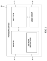
- the processing system 20 may be configured to implement one or more aspects of the present disclosure, however, the present disclosure is not limited to the particular processing system configuration shown in FIG. 1 .
- the processing system 20 includes a processor 22 in signal communication with memory 24.
- the processor 22 may be any type of computing device, computational circuit, or processing circuit capable of executing a series of instructions that are stored in memory 24.
- the processor 22 may include multiple processors and/or multicore CPUs and may include any type of processor, such as a microprocessor, digital signal processor, coprocessors, a micro-controller, a microcomputer, a central processing unit, a field programmable gate array, a programmable logic device, a state machine, logic circuitry, analog circuitry, digital circuitry, etc., and any combination thereof.
- processors such as a microprocessor, digital signal processor, coprocessors, a micro-controller, a microcomputer, a central processing unit, a field programmable gate array, a programmable logic device, a state machine, logic circuitry, analog circuitry, digital circuitry, etc., and any combination thereof.
- the memory 24 includes instructions stored therein.
- the instructions may represent one or more algorithms for controlling the aspects of the processing system 20, and the stored instructions are not limited to any particular form (e.g., program files, system data, buffers, drivers, utilities, system programs, etc.) provided they can be executed by the processor 22.
- the memory 24 may include software instructions 26 stored therein, which may be read and executed by the processor 22.
- the memory 24 may be a non-transitory computer readable storage medium configured to store instructions that when executed by the processor 22, cause the processor 22 to perform or cause the performance of certain functions.
- the memory 24 may be a single memory device or a plurality of memory devices.
- a memory device may include a storage area network, network attached storage, as well as a disk drive, a read-only memory, random access memory, volatile memory, non-volatile memory, static memory, dynamic memory, flash memory, cache memory, and/or any device that stores digital information.
- a storage area network may include a storage area network, network attached storage, as well as a disk drive, a read-only memory, random access memory, volatile memory, non-volatile memory, static memory, dynamic memory, flash memory, cache memory, and/or any device that stores digital information.
- the processor 22 may execute the software instructions 26 stored in memory 24 in a plurality of sequential software execution cycles.
- the software execution cycles may typically be performed as a fetch-execute cycle in which the processor 22 fetches the software instructions 26 from the memory 24, the processor 22 decodes the software instructions 26, and the processor 22 executes the software instructions 26. Once a software execution cycle is completed, the processor 22 begins a new software execution cycle until there are no additional software instructions.
- Each software execution cycle may have a predetermined software execution time DT which may be substantially constant among the plurality of software execution cycles for the given processor 22 and software instructions 26.
- the predetermined software execution time DT may have a value between approximately 1 millisecond and approximately 5 seconds. However, the present disclosure is not limited to any particular value of the predetermined software execution time DT.
- the processing system 20 includes at least one logic circuit 28.
- the logic circuit 28 is configured to receive an input signal 30 having an input signal value.
- the logic circuit 28 is further configured to provide an output signal 32, corresponding to the input signal value of the input signal 30, after a predetermined N value of time delay (e.g., N seconds).
- the logic circuit 28 is configured to provide a signal value as the output signal 32 after the predetermined N value of time delay.
- a detected condition, event, signal, or other occurrence may be determined based on one or more input signals to the processing system 20.
- the detected condition, event, signal, or other occurrence may cause the processing system 20 to evaluate the output signal 32.
- the processing system 20 may evaluate the signal value of the output signal 32 which is the same as the signal value of the input signal 30 from N seconds prior to the detected condition, event, signal, or other occurrence.
- the output signal 32 may be received by the processor 22 and used by the processor 22 for execution of the software instructions 26.
- the logic circuit 28 may be implemented using one or more logic inputs, one or more logic outputs, and a plurality of logic gates such as, but not limited to, NAND gates, XOR gates, and the like.
- the present disclosure logic circuit 28 allows a processing system, such as the processing system 20, to obtain a signal value from N seconds prior using a combination of switches, as will be discussed in further detail.
- the present disclosure logic circuit 28 may require less storage capacity than conventional processing structures, including array structures, to provide the signal value from N seconds prior.
- the memory array may require an array size of N seconds divided by an associated software execution time DT. Accordingly, the large size of a memory array circuit may, therefore, be undesirable for certain applications.
- the logic circuit 28 includes a plurality of switch assemblies 34.
- the plurality of switch assemblies 34 includes M number of switch assemblies 34. As will be discussed in further detail, the value of M for the number of switch assemblies 34 may be selected to determine, at least in part, the value of N for the predetermined value of time delay of the logic circuit 28.
- Each switch assembly 34 includes a switch 36.
- the switch 36 includes a true input gate 38, a false input gate 40, and a toggle input gate 42.
- the switch 36 further includes an output gate 44.
- Each switch assembly 34 further includes a first delay 46 and a second delay 48. The first delay 46 is in signal communication with the output gate 44. As shown in FIG.
- the first delay 46 for a first switch assembly 34 may be in signal communication between the output gate 44 for said first switch assembly 34 and the true input gate 38 for a second switch assembly 34 of the plurality of switch assemblies 34, which second switch assembly 34 is immediate downstream of the first switch assembly 34.
- the second delay 48 is in signal communication between the output gate 44 and the false input gate 40 for each switch assembly 34.
- the first delay 46 and the second delay 48 are configured to delay an input signal to the respective delay 46, 48 by one iteration of the predetermined software execution time DT.
- the plurality of switch assemblies 34 includes a signal input 50 and a signal output 52.
- the signal input 50 is configured to receive the input signal 30.
- the signal output 52 is configured to receive the output signal 32.
- the signal output 52 of the plurality of switch assemblies 34 may be in signal communication, directly or indirectly, with the processor 22.
- the plurality of switch assemblies 34 includes a leading switch assembly 34A and one or more trailing switch assemblies 34B.
- the true input gate 38 of the leading switch assembly 34A is in signal communication with the signal input 50.
- the true input gate 38 of each of the one or more trailing switch assemblies 34B is in signal communication with the first delay 46 of an immediately upstream switch assembly 34, as previously described.
- the one or more trailing switch assemblies 34B include a terminal switch assembly 34C.
- the first delay 46 of the terminal switch assembly 34C is in signal communication between the output gate 44 of the switch 36 for the terminal switch assembly 34C and the signal output 52.
- the logic circuit 28 includes a timer 54.
- the timer 54 includes an output gate 56 in signal communication with the respective toggle input gate 42 of each switch assembly 34 of the plurality of switch assemblies 34.
- the timer 54 is configured to provide a logic flag signal 58 ("ULAT") at the output gate 56 which coordinates the operation of the plurality of switch assemblies 34.
- TRUE e.g., a Boolean value of 1
- each switch assembly 34 passes the signal at the respective true input gate 38 to the respective output gate 44.
- the logic flag signal 58 is TRUE
- the signal value of the output signal 32 provided to the signal output 52 is updated with a new signal value corresponding to the value of signal value of the input signal 30 from N seconds prior.
- the logic flag signal 58 is FALSE (e.g., a Boolean value of 0)
- each switch assembly 34 passes the signal at the respective false input gate 40 to the respective output gate 44.
- the timer 54 may receive one or more input signals 60 which determine the operational characteristics of the timer 54.
- the timer 54 may receive a timer constant TM which controls a cycle time (e.g., in seconds) for the timer 54.
- the timer constant TM is substantially equal to the predetermined N value of time delay divided by the M number of switch assemblies 34 (e.g., TM may be substantially equal to N/M).
- the timer 54 may also receive the predetermined software execution time DT, where the predetermined software execution time DT represents the predetermined execution time of each software execution cycle for the software instructions 26 executed by the processor 22.
- the timer 54 counts the sequential software execution cycles having the software execution time DT until the elapsed time is equal to the timer constant TM, at which point the timer 54 changes the logic flag signal 58 to TRUE. It should be understood that, in some embodiments, the logic circuit 28 may not update the output signal 32 at the time precisely corresponding to the timer constant TM and the output signal 32 may alternatively be updated as soon as the number of sequential software execution cycles multiplied by the software execution time DT is greater than or equal to the N/M seconds (i.e., the timer constant TM).
- the logic circuit 28 of FIG. 3 may, therefore, be used to provide signal values for a particular processor 22 and associated software instructions 26 (see FIG. 1 ) having a predetermined software execution time DT of approximately 0.1 seconds for the processing system 20.
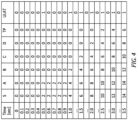
- FIG. 4 illustrates a value table showing signal values at various points (i.e., points S, A, B, C, D) of the logic circuit 28 of FIG. 3 , for each iteration of the timer constant TM.
- TP 2
Landscapes
- Engineering & Computer Science (AREA)
- Physics & Mathematics (AREA)
- Computer Hardware Design (AREA)
- Theoretical Computer Science (AREA)
- Nonlinear Science (AREA)
- Evolutionary Computation (AREA)
- Geometry (AREA)
- General Engineering & Computer Science (AREA)
- General Physics & Mathematics (AREA)
- Electronic Switches (AREA)
Abstract
Description
- This disclosure relates generally to processing systems for gas turbine engines and more particularly to logic circuits configured for storing a signal value for a predetermined time period.
- Control systems for gas turbine engines and other complex machinery must receive and store numerous electronic signals, and then process the electronic signals in an efficient manner. It some cases, it may be necessary to store electronic signal values for a predetermined period of time before they need to be read by the control system. Storage of the electronic signal values can require substantial amounts of storage capacity. Accordingly, systems and methods which reduce the storage capacity requirements for signal value storage are needed.
- It should be understood that any or all of the features or embodiments described herein can be used or combined in any combination with each and every other feature or embodiment described herein unless expressly noted otherwise.
- According to an aspect of the present disclosure, a logic circuit includes a timer and a plurality of switch assemblies in signal communication with the timer. Each switch assembly of the plurality of switch assemblies includes a switch including a true input gate, a false input gate, and an output gate, a first delay in signal communication with the output gate, and a second delay in signal communication between the output gate and the false input gate.
- In any of the aspects or embodiments described above and herein, the plurality of switch assemblies may include a first switch assembly and a second switch assembly and the first delay of the first switch assembly may be in signal communication between the output gate of the first switch assembly and the true input gate of the second switch assembly.
- In any of the aspects or embodiments described above and herein, the plurality of switch assemblies may include a signal input and a signal output and the plurality of switch assemblies may be configured to provide a signal value of the signal input to the signal output after a predetermined N value of time delay.
- In any of the aspects or embodiments described above and herein, the plurality of switch assemblies may include a leading switch assembly and one or more trailing switch assemblies and the true input gate of the switch of the leading switch assembly is in signal communication with the signal input.
- In any of the aspects or embodiments described above and herein, the one or more trailing switch assemblies may include a terminal switch assembly and the first delay of the terminal switch assembly may be in signal communication with the signal output.
- According to another aspect of the present disclosure, a processing system includes a non-transitory computer-readable storage medium having stored thereon software instructions and a processor configured to execute the software instructions over a plurality of sequential software execution cycles. Each software execution cycle of the plurality of sequential software execution cycles has a predetermined software execution time DT. The processing system further includes a logic circuit in signal communication with the processor. The logic circuit includes a timer and a plurality of switch assemblies comprising M number of switch assemblies. The plurality of switch assemblies is in signal communication with the timer. Each switch assembly of the plurality of switch assemblies includes a switch including a true input gate, a false input gate, and an output gate, a first delay in signal communication with the output gate, and a second delay in signal communication between the output gate and the false input gate.
- In any of the aspects or embodiments described above and herein, the plurality of switch assemblies may include a signal input and a signal output. The plurality of switch assemblies may be configured to provide a signal value of the signal input to the signal output after a predetermined N value of time delay.
- In any of the aspects or embodiments described above and herein, the signal output may be in signal communication with the processor.
- In any of the aspects or embodiments described above and herein, the processor may be configured to use the signal value during execution of the software instructions.
- In any of the aspects or embodiments described above and herein, the logic circuit may be configured to update the signal output at an interval corresponding to a timer constant TM of the timer. The timer constant TM may be substantially equal to the predetermined N value of time delay divided by the M number of switch assemblies.
- In any of the aspects or embodiments described above and herein, the M number of switch assemblies may be greater than or equal to two.
- In any of the aspects or embodiments described above and herein, the predetermined software execution time DT may have a value between 1 millisecond and 5 seconds.
- In any of the aspects or embodiments described above and herein, the first delay and the second delay may be configured to provide a time delay corresponding to one iteration of the predetermined software execution time DT.
- According to another aspect of the present disclosure, a method for providing a signal value to a signal output after a predetermined time period includes executing software instructions with a processor over a plurality of sequential software execution cycles. Each software execution cycle of the plurality of software execution cycles has a predetermined software execution time DT. The method further includes providing an output signal to the processor with a logic circuit. Providing the output signal to the processor includes providing a signal value of a signal input of the logic circuit to the processor via a signal output after a predetermined N value of time delay.
- In any of the aspects or embodiments described above and herein, the logic circuit may include a timer and a plurality of switch assemblies in signal communication with the timer. Each switch assembly of the plurality of switch assemblies may include a switch including a true input gate, a false input gate, and an output gate, a first delay in signal communication with the output gate, and a second delay in signal communication between the output gate and the false input gate.
- In any of the aspects or embodiments described above and herein, the method may further include updating the output signal at an interval corresponding to a timer constant TM of the timer.
- In any of the aspects or embodiments described above and herein, the predetermined software execution time DT may have a value between 1 millisecond and 5 seconds.
- In any of the aspects or embodiments described above and herein, the first delay and the second delay may be configured to provide a time delay corresponding to one iteration of the predetermined software execution time DT.
- In any of the aspects or embodiments described above and herein, the plurality of switch assemblies may include a leading switch assembly and one or more trailing switch assemblies and the true input gate of the switch of the leading switch assembly may be in signal communication with the signal input.
- In any of the aspects or embodiments described above and herein, the one or more trailing switch assemblies may include a terminal switch assembly and wherein the first delay of the terminal switch assembly is in signal communication with the signal output.
- The present disclosure, and all its aspects, embodiments and advantages associated therewith will become more readily apparent in view of the detailed description provided below, including the accompanying drawings.
-
-
FIG. 1 illustrates a block diagram of a processing system, in accordance with one or more embodiments of the present disclosure. -
FIG. 2 illustrates a Boolean diagram of a logic circuit, in accordance with one or more embodiments of the present disclosure. -
FIG. 3 illustrates a Boolean diagram of a logic circuit, in accordance with one or more embodiments of the present disclosure. -
FIG. 4 illustrates a variable table for the logic circuit ofFIG. 3 , in accordance with one or more embodiments of the present disclosure. - Referring to
FIG. 1 , a block diagram of anexemplary processing system 20 is shown. Theprocessing system 20 may be configured to implement one or more aspects of the present disclosure, however, the present disclosure is not limited to the particular processing system configuration shown inFIG. 1 . Theprocessing system 20 includes aprocessor 22 in signal communication withmemory 24. Theprocessor 22 may be any type of computing device, computational circuit, or processing circuit capable of executing a series of instructions that are stored inmemory 24. Theprocessor 22 may include multiple processors and/or multicore CPUs and may include any type of processor, such as a microprocessor, digital signal processor, coprocessors, a micro-controller, a microcomputer, a central processing unit, a field programmable gate array, a programmable logic device, a state machine, logic circuitry, analog circuitry, digital circuitry, etc., and any combination thereof. - The
memory 24 includes instructions stored therein. The instructions may represent one or more algorithms for controlling the aspects of theprocessing system 20, and the stored instructions are not limited to any particular form (e.g., program files, system data, buffers, drivers, utilities, system programs, etc.) provided they can be executed by theprocessor 22. For example, thememory 24 may includesoftware instructions 26 stored therein, which may be read and executed by theprocessor 22. Thememory 24 may be a non-transitory computer readable storage medium configured to store instructions that when executed by theprocessor 22, cause theprocessor 22 to perform or cause the performance of certain functions. Thememory 24 may be a single memory device or a plurality of memory devices. A memory device may include a storage area network, network attached storage, as well as a disk drive, a read-only memory, random access memory, volatile memory, non-volatile memory, static memory, dynamic memory, flash memory, cache memory, and/or any device that stores digital information. One skilled in the art will appreciate, based on a review of this disclosure, that the implementation of theprocessing system 20 may be achieved by the use of hardware, software, firmware, or any combination thereof. - The
processor 22 may execute thesoftware instructions 26 stored inmemory 24 in a plurality of sequential software execution cycles. The software execution cycles may typically be performed as a fetch-execute cycle in which theprocessor 22 fetches thesoftware instructions 26 from thememory 24, theprocessor 22 decodes thesoftware instructions 26, and theprocessor 22 executes thesoftware instructions 26. Once a software execution cycle is completed, theprocessor 22 begins a new software execution cycle until there are no additional software instructions. Each software execution cycle may have a predetermined software execution time DT which may be substantially constant among the plurality of software execution cycles for the givenprocessor 22 andsoftware instructions 26. The predetermined software execution time DT may have a value between approximately 1 millisecond and approximately 5 seconds. However, the present disclosure is not limited to any particular value of the predetermined software execution time DT. - Referring to
FIGS. 1 and2 , theprocessing system 20 includes at least onelogic circuit 28. Thelogic circuit 28 is configured to receive aninput signal 30 having an input signal value. Thelogic circuit 28 is further configured to provide anoutput signal 32, corresponding to the input signal value of theinput signal 30, after a predetermined N value of time delay (e.g., N seconds). In other words, thelogic circuit 28 is configured to provide a signal value as theoutput signal 32 after the predetermined N value of time delay. During execution of thesoftware instructions 26, a detected condition, event, signal, or other occurrence may be determined based on one or more input signals to theprocessing system 20. The detected condition, event, signal, or other occurrence may cause theprocessing system 20 to evaluate theoutput signal 32. In other words, theprocessing system 20 may evaluate the signal value of theoutput signal 32 which is the same as the signal value of theinput signal 30 from N seconds prior to the detected condition, event, signal, or other occurrence. - The
output signal 32 may be received by theprocessor 22 and used by theprocessor 22 for execution of thesoftware instructions 26. Thelogic circuit 28 may be implemented using one or more logic inputs, one or more logic outputs, and a plurality of logic gates such as, but not limited to, NAND gates, XOR gates, and the like. The presentdisclosure logic circuit 28 allows a processing system, such as theprocessing system 20, to obtain a signal value from N seconds prior using a combination of switches, as will be discussed in further detail. Moreover, the presentdisclosure logic circuit 28 may require less storage capacity than conventional processing structures, including array structures, to provide the signal value from N seconds prior. For example, for a memory array circuit to provide an output signal corresponding to a signal value of an input signal after a predetermined N value of time delay (e.g., N seconds), the memory array may require an array size of N seconds divided by an associated software execution time DT. Accordingly, the large size of a memory array circuit may, therefore, be undesirable for certain applications. - The
logic circuit 28 includes a plurality ofswitch assemblies 34. The plurality ofswitch assemblies 34 includes M number ofswitch assemblies 34. As will be discussed in further detail, the value of M for the number ofswitch assemblies 34 may be selected to determine, at least in part, the value of N for the predetermined value of time delay of thelogic circuit 28. Eachswitch assembly 34 includes aswitch 36. Theswitch 36 includes atrue input gate 38, afalse input gate 40, and atoggle input gate 42. Theswitch 36 further includes anoutput gate 44. Eachswitch assembly 34 further includes afirst delay 46 and asecond delay 48. Thefirst delay 46 is in signal communication with theoutput gate 44. As shown inFIG. 2 , thefirst delay 46 for afirst switch assembly 34 may be in signal communication between theoutput gate 44 for saidfirst switch assembly 34 and thetrue input gate 38 for asecond switch assembly 34 of the plurality ofswitch assemblies 34, whichsecond switch assembly 34 is immediate downstream of thefirst switch assembly 34. Thesecond delay 48 is in signal communication between theoutput gate 44 and thefalse input gate 40 for eachswitch assembly 34. Thefirst delay 46 and thesecond delay 48 are configured to delay an input signal to therespective delay - The plurality of
switch assemblies 34 includes asignal input 50 and asignal output 52. Thesignal input 50 is configured to receive theinput signal 30. Similarly, thesignal output 52 is configured to receive theoutput signal 32. Thesignal output 52 of the plurality ofswitch assemblies 34 may be in signal communication, directly or indirectly, with theprocessor 22. The plurality ofswitch assemblies 34 includes aleading switch assembly 34A and one or more trailingswitch assemblies 34B. Thetrue input gate 38 of theleading switch assembly 34A is in signal communication with thesignal input 50. Thetrue input gate 38 of each of the one or more trailingswitch assemblies 34B is in signal communication with thefirst delay 46 of an immediatelyupstream switch assembly 34, as previously described. The one or more trailingswitch assemblies 34B include aterminal switch assembly 34C. Thefirst delay 46 of theterminal switch assembly 34C is in signal communication between theoutput gate 44 of theswitch 36 for theterminal switch assembly 34C and thesignal output 52. - The
logic circuit 28 includes atimer 54. Thetimer 54 includes anoutput gate 56 in signal communication with the respectivetoggle input gate 42 of eachswitch assembly 34 of the plurality ofswitch assemblies 34. Thetimer 54 is configured to provide a logic flag signal 58 ("ULAT") at theoutput gate 56 which coordinates the operation of the plurality ofswitch assemblies 34. When thelogic flag signal 58 is TRUE (e.g., a Boolean value of 1), eachswitch assembly 34 passes the signal at the respectivetrue input gate 38 to therespective output gate 44. Thus, when thelogic flag signal 58 is TRUE, the signal value of theoutput signal 32 provided to thesignal output 52 is updated with a new signal value corresponding to the value of signal value of theinput signal 30 from N seconds prior. When thelogic flag signal 58 is FALSE (e.g., a Boolean value of 0), eachswitch assembly 34 passes the signal at the respectivefalse input gate 40 to therespective output gate 44. - The
timer 54 may receive one or more input signals 60 which determine the operational characteristics of thetimer 54. Thetimer 54 may receive a timer constant TM which controls a cycle time (e.g., in seconds) for thetimer 54. The timer constant TM is substantially equal to the predetermined N value of time delay divided by the M number of switch assemblies 34 (e.g., TM may be substantially equal to N/M). Thetimer 54 may also receive the predetermined software execution time DT, where the predetermined software execution time DT represents the predetermined execution time of each software execution cycle for thesoftware instructions 26 executed by theprocessor 22. Thetimer 54 counts the sequential software execution cycles having the software execution time DT until the elapsed time is equal to the timer constant TM, at which point thetimer 54 changes thelogic flag signal 58 to TRUE. It should be understood that, in some embodiments, thelogic circuit 28 may not update theoutput signal 32 at the time precisely corresponding to the timer constant TM and theoutput signal 32 may alternatively be updated as soon as the number of sequential software execution cycles multiplied by the software execution time DT is greater than or equal to the N/M seconds (i.e., the timer constant TM). - Referring to
FIGS. 3 and4 , an exemplary embodiment of thelogic circuit 28 is provided. Thelogic circuit 28 ofFIG. 3 includes four switch assemblies 34 (e.g., M = 4) and has a predetermined N value of time delay of two seconds (e.g., N = 2 seconds). Accordingly, thetimer 54 of thelogic circuit 28 ofFIG. 3 may have a timer constant TM of 0.5 seconds. Thelogic circuit 28 ofFIG. 3 may, therefore, be used to provide signal values for aparticular processor 22 and associated software instructions 26 (seeFIG. 1 ) having a predetermined software execution time DT of approximately 0.1 seconds for theprocessing system 20. -
FIG. 4 illustrates a value table showing signal values at various points (i.e., points S, A, B, C, D) of thelogic circuit 28 ofFIG. 3 , for each iteration of the timer constant TM. In a first example of the operation of thelogic circuit 28 ofFIG. 3 , thesignal input 50 of the plurality ofswitch assemblies 34 receives theinput signal 30 having a signal value of two (e.g., S = 2) at 0.5 seconds. At approximately 2.5 seconds, thesignal output 52 of the plurality ofswitch assemblies 34 receives theoutput signal 32 having the signal value of two (e.g., TP = 2). Similarly, in a second example of the operation of thelogic circuit 28 ofFIG. 3 , thesignal input 50 of the plurality ofswitch assemblies 34 receives theinput signal 30 having a signal value of four (e.g., S = 4) at 1.0 seconds. At approximately 3.0 seconds, thesignal output 52 of the plurality ofswitch assemblies 34 receives theoutput signal 32 having the signal value of four (e.g., TP = 4). - It is noted that various connections are set forth between elements in the preceding description and in the drawings. It is noted that these connections are general and, unless specified otherwise, may be direct or indirect and that this specification is not intended to be limiting in this respect. A coupling between two or more entities may refer to a direct connection or an indirect connection. An indirect connection may incorporate one or more intervening entities. It is further noted that various method or process steps for embodiments of the present disclosure are described in the following description and drawings. The description may present the method and/or process steps as a particular sequence. However, to the extent that the method or process does not rely on the particular order of steps set forth herein, the method or process should not be limited to the particular sequence of steps described. As one of ordinary skill in the art would appreciate, other sequences of steps may be possible. Therefore, the particular order of the steps set forth in the description should not be construed as a limitation.
- Furthermore, no element, component, or method step in the present disclosure is intended to be dedicated to the public regardless of whether the element, component, or method step is explicitly recited in the claims. No claim element herein is to be construed under the provisions of 35 U.S.C. 112(f) unless the element is expressly recited using the phrase "means for." As used herein, the terms "comprises", "comprising", or any other variation thereof, are intended to cover a non-exclusive inclusion, such that a process, method, article, or apparatus that comprises a list of elements does not include only those elements but may include other elements not expressly listed or inherent to such process, method, article, or apparatus.
- While various aspects of the present disclosure have been disclosed, it will be apparent to those of ordinary skill in the art that many more embodiments and implementations are possible within the scope of the present disclosure. For example, the present disclosure as described herein includes several aspects and embodiments that include particular features. Although these particular features may be described individually, it is within the scope of the present disclosure that some or all of these features may be combined with any one of the aspects and remain within the scope of the present disclosure. References to "various embodiments," "one embodiment," "an embodiment," "an example embodiment," etc., indicate that the embodiment described may include a particular feature, structure, or characteristic, but every embodiment may not necessarily include the particular feature, structure, or characteristic. Moreover, such phrases are not necessarily referring to the same embodiment. Further, when a particular feature, structure, or characteristic is described in connection with an embodiment, it is submitted that it is within the knowledge of one skilled in the art to effect such feature, structure, or characteristic in connection with other embodiments whether or not explicitly described. Accordingly, the present disclosure is not to be restricted except in light of the attached claims and their equivalents.
Claims (13)
- A logic circuit comprising:a timer; anda plurality of switch assemblies in signal communication with the timer, each switch assembly of the plurality of switch assemblies including:a switch including a true input gate, a false input gate, and an output gate;a first delay in signal communication with the output gate; anda second delay in signal communication between the output gate and the false input gate.
- The logic circuit of claim 1, wherein the plurality of switch assemblies includes a first switch assembly and a second switch assembly and wherein the first delay of the first switch assembly is in signal communication between the output gate of the first switch assembly and the true input gate of the second switch assembly.
- The logic circuit of claim 1 or 2, wherein the plurality of switch assemblies includes a signal input and a signal output and wherein the plurality of switch assemblies is configured to provide a signal value of the signal input to the signal output after a predetermined N value of time delay.
- The logic circuit of claim 3, wherein the plurality of switch assemblies includes a leading switch assembly and one or more trailing switch assemblies and wherein the true input gate of the switch of the leading switch assembly is in signal communication with the signal input.
- The logic circuit of claim 4, wherein the one or more trailing switch assemblies includes a terminal switch assembly and wherein the first delay of the terminal switch assembly is in signal communication with the signal output.
- A processing system comprising:a non-transitory computer-readable storage medium having stored thereon software instructions;a processor configured to execute the software instructions over a plurality of sequential software execution cycles, each software execution cycle of the plurality of sequential software execution cycles having a predetermined software execution time DT; andthe logic circuit of claim 1, the logic circuit in signal communication with the processor, the plurality of switch assemblies comprising M number of switch assemblies.
- The processing system of claim 6, wherein the plurality of switch assemblies includes a signal input and a signal output, wherein the plurality of switch assemblies is configured to provide a signal value of the signal input to the signal output after a predetermined N value of time delay.
- The processing system of claim 7, wherein the signal output is in signal communication with the processor.
- The processing system of claim 8, wherein the processor is configured to use the signal value during execution of the software instructions.
- The processing system of any of claims 7 to 9, wherein the logic circuit is configured to update the signal output at an interval corresponding to a timer constant TM of the timer, the timer constant TM is substantially equal to the predetermined N value of time delay divided by the M number of switch assemblies.
- The processing system of claim 10, wherein the M number of switch assemblies is greater than or equal to two.
- The processing system of any of claims 6 to 11, wherein the predetermined software execution time DT has a value between 1 millisecond and 5 seconds.
- The processing system of any of claims 6 to 12, wherein the first delay and the second delay are configured to provide a time delay corresponding to one iteration of the predetermined software execution time DT.
Applications Claiming Priority (1)
| Application Number | Priority Date | Filing Date | Title |
|---|---|---|---|
| US17/670,128 US12278624B2 (en) | 2022-02-11 | 2022-02-11 | Logic circuit for providing a signal value after a predetermined time period and method of using same |
Publications (1)
| Publication Number | Publication Date |
|---|---|
| EP4228156A1 true EP4228156A1 (en) | 2023-08-16 |
Family
ID=85238943
Family Applications (1)
| Application Number | Title | Priority Date | Filing Date |
|---|---|---|---|
| EP23156407.1A Pending EP4228156A1 (en) | 2022-02-11 | 2023-02-13 | Logic circuit for providing a signal value after a predetermined time period and method of using same |
Country Status (3)
| Country | Link |
|---|---|
| US (1) | US12278624B2 (en) |
| EP (1) | EP4228156A1 (en) |
| CA (1) | CA3189528A1 (en) |
Citations (3)
| Publication number | Priority date | Publication date | Assignee | Title |
|---|---|---|---|---|
| US20180108388A1 (en) * | 2016-10-18 | 2018-04-19 | Taiwan Semiconductor Manufacturing Company Limited | Selectable Delay Buffers and Logic Cells for Dynamic Voltage Scaling in Ultra Low Voltage Designs |
| US10877541B1 (en) * | 2019-12-30 | 2020-12-29 | Micron Technology, Inc. | Power delivery timing for memory |
| US10958255B1 (en) * | 2019-12-27 | 2021-03-23 | Intel Corporation | Frequency doubler pulse limiter and methods for limiting pulse widths produced by a frequency doubler |
Family Cites Families (33)
| Publication number | Priority date | Publication date | Assignee | Title |
|---|---|---|---|---|
| US3845324A (en) * | 1972-12-22 | 1974-10-29 | Teletype Corp | Dual voltage fet inverter circuit with two level biasing |
| US3851258A (en) * | 1973-12-13 | 1974-11-26 | Rca Corp | Gateless logic for producing selectable phase clock pulses |
| US4638183A (en) * | 1984-09-20 | 1987-01-20 | International Business Machines Corporation | Dynamically selectable polarity latch |
| US4691122A (en) * | 1985-03-29 | 1987-09-01 | Advanced Micro Devices, Inc. | CMOS D-type flip-flop circuits |
| US4800300A (en) * | 1987-11-02 | 1989-01-24 | Advanced Micro Devices, Inc. | High-performance, CMOS latch for improved reliability |
| US5216299A (en) * | 1992-02-13 | 1993-06-01 | Standard Microsystems Corporation | Low power noise rejecting TTL to CMOS input buffer |
| US5481500A (en) * | 1994-07-22 | 1996-01-02 | International Business Machines Corporation | Precharged bit decoder and sense amplifier with integrated latch usable in pipelined memories |
| US5424654A (en) * | 1994-09-22 | 1995-06-13 | Kaplinsky; Cecil H. | Programmable macrocell circuit |
| US5689257A (en) * | 1996-01-05 | 1997-11-18 | Analog Devices, Inc. | Skewless differential switch and DAC employing the same |
| US5920222A (en) * | 1997-04-22 | 1999-07-06 | International Business Machines Corporation | Tunable pulse generator based on a wave pipeline |
| US5973508A (en) * | 1997-05-21 | 1999-10-26 | International Business Machines Corp. | Voltage translation circuit for mixed voltage applications |
| US6356102B1 (en) * | 1998-11-13 | 2002-03-12 | Integrated Device Technology, Inc. | Integrated circuit output buffers having control circuits therein that utilize output signal feedback to control pull-up and pull-down time intervals |
| US6529040B1 (en) * | 2000-05-05 | 2003-03-04 | Xilinx, Inc. | FPGA lookup table with speed read decoder |
| JP2002100189A (en) * | 2000-09-22 | 2002-04-05 | Mitsubishi Electric Corp | Semiconductor device |
| JP4071604B2 (en) | 2002-11-18 | 2008-04-02 | 株式会社ルネサステクノロジ | Information processing apparatus provided with clock generation circuit and information processing apparatus provided with clock delay circuit |
| US6822885B2 (en) * | 2003-04-14 | 2004-11-23 | International Business Machines Corporation | High speed latch and compare function |
| US6741111B1 (en) * | 2003-04-21 | 2004-05-25 | Pericom Semiconductor Corp. | Data register for buffering double-data-rate DRAMs with reduced data-input-path power consumption |
| US7064595B2 (en) * | 2003-12-26 | 2006-06-20 | Stmicroelectronics Pvt Ltd. | Differential input receiver |
| US7564263B2 (en) * | 2005-04-21 | 2009-07-21 | Supertex, Inc. | High-speed logic signal level shifter |
| US20080180139A1 (en) * | 2007-01-29 | 2008-07-31 | International Business Machines Corporation | Cmos differential rail-to-rail latch circuits |
| US7834663B2 (en) * | 2007-04-18 | 2010-11-16 | Oracle America, Inc. | NAND/NOR registers |
| US20090108885A1 (en) * | 2007-10-31 | 2009-04-30 | International Business Machines Corporation | Design structure for CMOS differential rail-to-rail latch circuits |
| US7898283B1 (en) | 2009-08-31 | 2011-03-01 | Farinaz Koushanfar | Lightweight secure physically unclonable functions |
| WO2012147187A1 (en) | 2011-04-27 | 2012-11-01 | トヨタ自動車株式会社 | Periphery vehicle detection device |
| US9147620B2 (en) * | 2012-03-28 | 2015-09-29 | Teradyne, Inc. | Edge triggered calibration |
| US9372499B2 (en) * | 2014-01-21 | 2016-06-21 | Advanced Micro Devices, Inc. | Low insertion delay clock doubler and integrated circuit clock distribution system using same |
| US9471094B1 (en) | 2014-12-30 | 2016-10-18 | Cadence Design Systems, Inc. | Method of aligning timing of a chip select signal with a cycle of a memory device |
| JP6803657B2 (en) | 2015-08-31 | 2020-12-23 | 日立オートモティブシステムズ株式会社 | Vehicle control device and vehicle control system |
| JP6521468B2 (en) | 2017-06-15 | 2019-05-29 | 株式会社Subaru | Automatic steering control device |
| US11336271B2 (en) * | 2018-10-16 | 2022-05-17 | Sony Semiconductor Solutions Corporation | Data holding circuit |
| US11029720B2 (en) * | 2019-04-16 | 2021-06-08 | Intel Corporation | Area-efficient scalable memory read-data multiplexing and latching |
| US12095366B2 (en) * | 2021-04-06 | 2024-09-17 | Semiconductor Components Industries, Llc | Current limiting circuit |
| US20240371430A1 (en) * | 2023-05-05 | 2024-11-07 | Micron Technology, Inc. | Serializer clocking scheme for a memory device |
-
2022
- 2022-02-11 US US17/670,128 patent/US12278624B2/en active Active
-
2023
- 2023-02-09 CA CA3189528A patent/CA3189528A1/en active Pending
- 2023-02-13 EP EP23156407.1A patent/EP4228156A1/en active Pending
Patent Citations (3)
| Publication number | Priority date | Publication date | Assignee | Title |
|---|---|---|---|---|
| US20180108388A1 (en) * | 2016-10-18 | 2018-04-19 | Taiwan Semiconductor Manufacturing Company Limited | Selectable Delay Buffers and Logic Cells for Dynamic Voltage Scaling in Ultra Low Voltage Designs |
| US10958255B1 (en) * | 2019-12-27 | 2021-03-23 | Intel Corporation | Frequency doubler pulse limiter and methods for limiting pulse widths produced by a frequency doubler |
| US10877541B1 (en) * | 2019-12-30 | 2020-12-29 | Micron Technology, Inc. | Power delivery timing for memory |
Also Published As
| Publication number | Publication date |
|---|---|
| US12278624B2 (en) | 2025-04-15 |
| US20230261649A1 (en) | 2023-08-17 |
| CA3189528A1 (en) | 2023-08-11 |
Similar Documents
| Publication | Publication Date | Title |
|---|---|---|
| US4097920A (en) | Hardware control for repeating program loops in electronic computers | |
| US6209086B1 (en) | Method and apparatus for fast response time interrupt control in a pipelined data processor | |
| KR20040016829A (en) | Exception handling in a pipelined processor | |
| JP3242508B2 (en) | Microcomputer | |
| US20110093683A1 (en) | Program flow control | |
| EP3765963B1 (en) | Tracing branch instructions | |
| US7890800B2 (en) | Method, operating system and computing hardware for running a computer program | |
| US5179693A (en) | System for controlling operation of processor by adjusting duty cycle of performance control pulse based upon target performance value | |
| US12278624B2 (en) | Logic circuit for providing a signal value after a predetermined time period and method of using same | |
| US10540299B2 (en) | Resetting operating state holding element | |
| CN108701031B (en) | Register Access Control | |
| CN101989190B (en) | Wait instruction | |
| KR100521110B1 (en) | Event handling | |
| US7971040B2 (en) | Method and device for saving and restoring a set of registers of a microprocessor in an interruptible manner | |
| KR20180034508A (en) | Data processing | |
| US20210124635A1 (en) | Multicore system | |
| CN111045730A (en) | Hardware fast interrupt processing system and method for RISC-V architecture | |
| JP2000194556A (en) | Instruction look-ahead system and hardware | |
| CN116248088B (en) | Data delay method, device, circuit, electronic equipment and readable storage medium | |
| JP3100705B2 (en) | Apparatus for instruction preparation in a microprocessor | |
| JP3231505B2 (en) | MPU emulator device | |
| JPH03246603A (en) | Rapid counter | |
| EP0260639A2 (en) | Microprogram sequencer | |
| JP2710558B2 (en) | Information processing device | |
| CN119179556A (en) | Interrupt management method, interrupt management device, computer equipment and computer readable storage medium |
Legal Events
| Date | Code | Title | Description |
|---|---|---|---|
| PUAI | Public reference made under article 153(3) epc to a published international application that has entered the european phase |
Free format text: ORIGINAL CODE: 0009012 |
|
| STAA | Information on the status of an ep patent application or granted ep patent |
Free format text: STATUS: THE APPLICATION HAS BEEN PUBLISHED |
|
| AK | Designated contracting states |
Kind code of ref document: A1 Designated state(s): AL AT BE BG CH CY CZ DE DK EE ES FI FR GB GR HR HU IE IS IT LI LT LU LV MC ME MK MT NL NO PL PT RO RS SE SI SK SM TR |
|
| STAA | Information on the status of an ep patent application or granted ep patent |
Free format text: STATUS: REQUEST FOR EXAMINATION WAS MADE |
|
| 17P | Request for examination filed |
Effective date: 20240216 |
|
| RBV | Designated contracting states (corrected) |
Designated state(s): AL AT BE BG CH CY CZ DE DK EE ES FI FR GB GR HR HU IE IS IT LI LT LU LV MC ME MK MT NL NO PL PT RO RS SE SI SK SM TR |
|
| STAA | Information on the status of an ep patent application or granted ep patent |
Free format text: STATUS: EXAMINATION IS IN PROGRESS |
|
| 17Q | First examination report despatched |
Effective date: 20251114 |