EP4224711A1 - Quadrature clock generator with duty cycle corrector - Google Patents
Quadrature clock generator with duty cycle corrector Download PDFInfo
- Publication number
- EP4224711A1 EP4224711A1 EP23154185.5A EP23154185A EP4224711A1 EP 4224711 A1 EP4224711 A1 EP 4224711A1 EP 23154185 A EP23154185 A EP 23154185A EP 4224711 A1 EP4224711 A1 EP 4224711A1
- Authority
- EP
- European Patent Office
- Prior art keywords
- clock
- signal
- clock signal
- time control
- control signal
- Prior art date
- Legal status (The legal status is an assumption and is not a legal conclusion. Google has not performed a legal analysis and makes no representation as to the accuracy of the status listed.)
- Pending
Links
Images





Classifications
-
- G—PHYSICS
- G06—COMPUTING OR CALCULATING; COUNTING
- G06F—ELECTRIC DIGITAL DATA PROCESSING
- G06F1/00—Details not covered by groups G06F3/00 - G06F13/00 and G06F21/00
- G06F1/04—Generating or distributing clock signals or signals derived directly therefrom
- G06F1/14—Time supervision arrangements, e.g. real time clock
-
- H—ELECTRICITY
- H03—ELECTRONIC CIRCUITRY
- H03K—PULSE TECHNIQUE
- H03K5/00—Manipulating of pulses not covered by one of the other main groups of this subclass
- H03K5/156—Arrangements in which a continuous pulse train is transformed into a train having a desired pattern
- H03K5/1565—Arrangements in which a continuous pulse train is transformed into a train having a desired pattern the output pulses having a constant duty cycle
-
- G—PHYSICS
- G06—COMPUTING OR CALCULATING; COUNTING
- G06F—ELECTRIC DIGITAL DATA PROCESSING
- G06F1/00—Details not covered by groups G06F3/00 - G06F13/00 and G06F21/00
- G06F1/04—Generating or distributing clock signals or signals derived directly therefrom
- G06F1/08—Clock generators with changeable or programmable clock frequency
-
- H—ELECTRICITY
- H04—ELECTRIC COMMUNICATION TECHNIQUE
- H04L—TRANSMISSION OF DIGITAL INFORMATION, e.g. TELEGRAPHIC COMMUNICATION
- H04L27/00—Modulated-carrier systems
- H04L27/32—Carrier systems characterised by combinations of two or more of the types covered by groups H04L27/02, H04L27/10, H04L27/18 or H04L27/26
- H04L27/34—Amplitude- and phase-modulated carrier systems, e.g. quadrature-amplitude modulated carrier systems
- H04L27/38—Demodulator circuits; Receiver circuits
- H04L27/3845—Demodulator circuits; Receiver circuits using non - coherent demodulation, i.e. not using a phase synchronous carrier
- H04L27/3854—Demodulator circuits; Receiver circuits using non - coherent demodulation, i.e. not using a phase synchronous carrier using a non - coherent carrier, including systems with baseband correction for phase or frequency offset
- H04L27/3863—Compensation for quadrature error in the received signal
Definitions
- This disclosure relates generally to circuits and techniques for digital clock generation, and more specifically to the generation of quadrature clock signals.
- quadrature clocks may include an in-phase clock signal, and a quadrature phase clock signal, where the quadrature phase clock signal has the same frequency and amplitude as the in-phase clock signal, but is shifted in phase by a quarter wavelength, in other words, shifted by 90° or ⁇ /2 radians.
- Circuitry for generating such quadrature clock signals may be configured to maintain appropriate duty cycles, amplitudes, and frequencies for each of the in-phase and quadrature phase clock signals, as well as to maintain the quarter wavelength phase difference between the in-phase clock signal and the quadrature phase clock signal.
- An example quadrature clock generator includes an in-phase (I) clock generation circuit to generate an I clock signal based on a reference clock signal, the I clock signal and the reference clock signal each having a first frequency, a quadrature phase (Q) clock generation circuit to generate a Q clock signal based on the reference clock signal, a rise time control signal, and a fall time control signal, the Q clock signal having the first frequency, and a control circuit to generate the rise time control signal and the fall time control signal based on the I clock signal and the Q clock signal.
- I in-phase
- Q quadrature phase
- An example dual rail quadrature clock generator includes an in-phase (I) clock generation circuit to generate a noninverted I clock signal and an inverted I clock signal based on a noninverted reference clock signal and an inverted reference clock signal, the noninverted I clock signal, the inverted I clock signal, the noninverted reference clock signal and the inverted reference clock signal each having a first frequency, a quadrature phase (Q) clock generation circuit to generate a noninverted Q clock signal and an inverted Q clock signal based on the noninverted reference clock signal, the inverted reference clock signal, the noninverted I clock signal, and the inverted Q clock signal, wherein the noninverted Q clock signal and the inverted Q clock signal have the first frequency, and a control circuit to generate a rise time control signal and a fall time control signal for adjusting a rise time and a fall time of the noninverted Q clock signal and the inverted Q clock signal, wherein the rise time control signal and
- a single block may be described as performing a function or functions; however, in actual practice, the function or functions performed by that block may be performed in a single component or across multiple components, and/or may be performed using hardware, using software, or using a combination of hardware and software.
- various illustrative components, blocks, modules, circuits, and steps have been described below generally in terms of their functionality. Whether such functionality is implemented as hardware or software depends upon the particular application and design constraints imposed on the overall system. Skilled artisans may implement the described functionality in varying ways for each particular application, but such implementation decisions should not be interpreted as causing a departure from the scope of the present disclosure.
- the example input devices may include components other than those shown, including well-known components such as a processor, memory and the like.
- the techniques described herein may be implemented in hardware, software, firmware, or any combination thereof, unless specifically described as being implemented in a specific manner. Any features described as modules or components may also be implemented together in an integrated logic device or separately as discrete but interoperable logic devices. If implemented in software, the techniques may be realized at least in part by a non-transitory processor-readable storage medium comprising instructions that, when executed, performs one or more of the methods described above.
- the non-transitory processor-readable data storage medium may form part of a computer program product, which may include packaging materials.
- an in-phase (I) clock generation circuit generates an I clock signal based on a reference clock signal, such as by delaying the reference clock signal.
- the I clock signal has the same frequency as the reference clock signal.
- a quadrature phase (Q) clock generation circuit generates a Q clock signal based on the reference clock signal, a rise time control signal, and a fall time control signal.
- the Q clock signal has the same frequency as the I clock signal (and the reference clock signal) but is offset in phase by 90 degrees with respect to the I clock signal.
- a control circuit generates the rise time control signal and the fall time control signal based on the I clock signal and the Q clock signal.
- the rise time control signal and the fall time control signal are used by the Q clock generation circuit in order to maintain the 90 degrees phase offset between the I clock signal and the Q clock signal and to maintain the proper 50% duty cycle for the Q clock signal.
- the reference clock signal or signals required for the example implementations have the same frequency as the quadrature clock signals generated by the example circuits. This may result in reduced power consumption and heat generation.
- the example implementations may generate the quadrature clock signals accurately, by determining the phase difference between the I and Q clock signals and correcting for phase mismatch by locking the delay to a 90 degree phase delay between the I and Q clock signals. Further, the example implementations may correct any duty cycle mismatches in the Q clock signals in order to ensure accurate clock signal generation for a wide variety of desired clock frequencies.
- FIG. 1A shows a conventional digital phase splitter circuit 100A, which may be used to generate quadrature clock signals.
- the digital phase splitter circuit 100A may include a first flip-flop 120, a second flip-flop 130, and an inverter 140. Note that, while the first flip-flop 120 and second flip-flop 130 are shown as D flip-flops, other conventional digital phase splitter circuits may use other types of flip-flops or latches.
- the first flip-flop 120 may be clocked by a reference clock signal 110, while an in-phase clock 150 may be generated at the output Q.
- the output Q_bar may be provided at the input D of the first flip-flop 120.
- the reference clock 110 may be provided to the inverter 140, and the output of the inverter 140 is provided to the input D and the output Q_bar of the second flip-flop 130.
- the quadrature phase clock 160 may be generated at the output Q_bar of the second flip-flop 130.
- the in-phase clock 150 and the quadrature-phase clock 160 may each have a frequency which is half that of the reference clock 110. In other words, for a desired frequency of the clock signals 150 and 160, a reference clock 110 having twice the frequency is required.
- FIG. 1B shows a timing diagram 100B of the input and output signals of the digital phase splitter circuit 100A.
- the reference clock 110 has twice the frequency of the in-phase clock 150 and twice the frequency of the quadrature phase clock 160.
- the reference clock period 111 is half of the output clock period 151.
- the phase offset 161 between the quadrature phase clock 160 and the in-phase clock 150 is one quarter of the output clock period 161.
- FIG. 2 shows a conventional delay locked loop (DLL) circuit 200 for generating quadrature clock signals.
- the DLL circuit 200 includes four delay cells 220(1)-220(4) (collectively delay cells 220). Each delay cell is configured to delay a reference clock 210 by one quarter wavelength.
- each delay cell of the delay cells 220 may include an inverter and a capacitor, or another suitable circuit for delaying an input signal.
- the reference clock 210 may be delayed by one quarter wavelength, or 90 degrees.
- the remaining delay stages may have identical structure, such that the second delay cell 220(2) outputs a signal corresponding to the reference clock 210 which has been delayed by one half wavelength, or 180 degrees.
- the third delay call 220(3) outputs a signal corresponding to the reference clock 210 delayed by three quarters of a wavelength, or 270 degrees
- the fourth delay cell 220(4) outputs a signal which should be in phase with the reference clock 210.
- the DLL circuit 200 outputs an in-phase clock 250, which may simply be the reference clock 210, and a quadrature phase clock 260, which may be the output of the first delay cell 220(1).
- the DLL circuit 200 also includes a delay locked loop 230, which may receive the reference clock 210 and the output of the fourth delay cell 220(4) and generate delay control signals for the delay cells 220.
- the delay locked loop 230 may generate the delay control signals to correct for any mismatch between the reference clock 210 and the output of the delay cell 220(4), which should be identical and in phase with the reference clock 210.
- the digital phase splitter circuit 100A and the DLL circuit 200 may be used to generate quadrature clock signals, they each have drawbacks.
- the digital phase splitter circuit 100A requires a reference clock signal having twice the frequency of the desired quadrature clock signals. This may result in undesirably high power consumption or circuit complexity for generating such high frequency reference clock signals.
- chip to chip speeds are increasing due to the bandwidth needs of high-capacity network and high-performance computer systems, which may use high resolution video applications such as 4k and 8k.
- interfaces may be required to support a variety of data rates as well, such as 5.4 Gbps, 6.75Gbps, 8.1 Gbps, 10 Gbps, 13.5 Gbps, 20Gbps, and so on, for backward compatibility and for low power consumption.
- the digital phase splitter circuit 100A cannot easily adjust for inaccurate duty cycles or phase offsets, which may result in inaccurate clock signals.
- the DLL circuit 200 may result in a quadrature clock 260 having a distorted duty cycle, as the duty cycle is not controlled and may be distorted by the delay cells 220 of the DLL circuit 200. Further, the DLL circuit 200 may experience harmonic locking issues, when the delay provided by the delay locked loop 230 and the delay cells 220 may not lock to one wavelength, but may lock to an integer N number of wavelengths. This may result in functional issues with the DLL circuit 200, or may require additional circuitry to avoid these harmonic locking issues. Further, the delay cells 220 are difficult to match, and may not each provide precisely the same amount of delay, which may result in IQ phase delay errors due to this delay cell mismatch.
- the example implementations may generate quadrature clock signals using fully differential amplifier circuitry, and which may detect the phase difference between the in-phase (I) and quadrature phase (Q) clock signals using phase detection, and adjust the phase offset and duty cycle of the Q clock signals to maintain its desired quarter wavelength offset and 50% duty cycle.
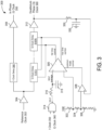
- FIG. 3 shows an example quadrature clock generator 300, according to some implementations.
- the quadrature clock generator 300 receives a reference clock 302, which may optionally be buffered by a buffer 304.
- the buffered reference clock 302 may be provided to an I clock delay circuit 306 and one or more Q clock delay circuits 310(1)-310(N) (collectively Q clock delay circuits 310).
- the I clock delay circuit may delay the reference clock 302, generating an I clock 350 which may optionally be buffered by a buffer 308.
- This I clock 350 has the same frequency as the reference clock 302.
- the Q clock delay circuits 310 may each delay and adjust a phase offset and duty cycle of the reference clock 302 in order to generate the Q clock 360, which may optionally be buffered by a buffer 312.
- the Q clock 360 also has the same frequency as the reference clock 302, but is shifted in phase by one quarter wavelength.
- Each Q clock delay circuit 310 may also receive a fall time control signal and a rise time control signal, which may be used by the Q clock delay circuits 310 to adjust the phase offset and duty cycles, as discussed in more detail below.
- the fall time control signal and the rise time control signal may be generated by a control circuit including a NAND gate 314, a resistor 316, a capacitor 318, a differential amplifier 320, resistors 322, 324, and 326, an amplifier 328, a resistor 330, and a capacitor 332.
- the NAND gate 314 may receive the I clock 350 at a noninverting input, and the Q clock 360 at an inverting input, outputting an "iqout" signal, which may correspond to a phase difference between the I clock 350 and the Q clock 360. For example, when the I clock 350 and the Q clock 360 have the desired quarter wavelength, or 90 degree, phase difference, the iqout signal may have a 75% duty cycle.
- the NAND gate 314 may be replaced by a suitable IQ phase detect circuit, as described below.
- the resistor 316 and capacitor 318 may generate an "iqout average" signal representing an average value of iqout.
- iqout average has a value of 75% of a supply voltage of the quadrature clock generator 300, such as 75% of Vdd.
- Iqout average may be provided at a noninverting input of the differential amplifier 320.
- the resistors 322, 324, and 326 may be used to generate another signal having a value of 75% of Vdd, which may be provided at an inverting input of the differential amplifier 320.
- the fall time control signal provided from an inverting output of the differential amplifier 320
- the rise time control signal provided from a noninverting output of the differential amplifier 320, may be based on the phase offset between the I clock 350 and the Q clock 360.
- the quadrature clock generator 300 may also provide duty cycle correction for the Q clock 360.
- the output common mode voltage control for the differential amplifier 320 may be provided from an output of the amplifier 328.
- the amplifier 328 has an inverting input coupled to receive a signal having a value of 50% of Vdd, corresponding to an intended 50% duty cycle of the Q clock 360.
- a noninverting input of the amplifier 328 may be coupled to receive a signal corresponding to an average value of the Q clock 360. This average value of the Q clock 360 may be generated from the Q clock 360 using the resistor 330 and the capacitor 332.
- the output of the amplifier 328 controls rise time and fall time of Q clock delay circuits 310 by controlling the output common mode voltage of the differential amplifier 320 to adjust Q clock 360 duty cycle to 50% because the output of the amplifier 328 is based on a difference between the desired 50% duty cycle of Q clock 360-represented by the inverting input to the amplifier 328-and the actual duty cycle of the Q clock 360-represented by the noninverting input to the amplifier 328.
- averaging circuits in FIG. 3 are shown as a resistor and a capacitor, such as the resistor 316 and capacitor 318, that in other aspects other suitable circuits may be used for generating the average signal values.
- FIG. 4 shows an example I clock delay circuit 400, which may be one example of the I clock delay circuit 306 shown in FIG. 3 .
- the I clock delay circuit 400 may include a simple inverter chain, such as including the inverters 410 and 430. In other aspects, the I clock delay circuits may include any number of inverters, provided that the output is not inverted with respect to the input.
- the I clock delay circuit 400 may also include a capacitor 420. Note that for higher frequency clocks, for example for 10 GHz clock, that a minimum delay for the Q clock delay circuits may be higher than the desired 90 degree phase difference between the I and Q clocks.
- Example quadrature clock generator circuits for such high frequency clocks may include an artificial delay added to the I clock delay circuits, such as the I clock delay circuits 306 or 400, in order to reduce the I clock to Q clock phase delay difference to the desired 90 degrees.
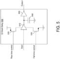
- FIG. 5 shows an example Q clock delay circuit 500, which may be one example of each of the Q clock delay circuits 310 of FIG. 3 .
- the Q clock delay circuit 500 may receive the rise time control signal and the fall time control signal, such as from the differential amplifier 320.
- the Q clock delay circuit 500 may also receive an input, such as the reference clock 302, or an output from a previous Q clock delay circuit. This input signal may be provided to an inverter 510.
- a supply terminal of the inverter 510 may be coupled to a drain terminal of a transistor 520, which may be a P-channel metal-oxide-semiconductor (PMOS) transistor.
- PMOS metal-oxide-semiconductor
- a source terminal of the transistor 520 may be coupled to a supply voltage, and a gate terminal of the transistor 520 may be coupled to the rise time control signal.
- a ground terminal of the inverter 510 may be coupled to a drain terminal of a transistor 530, which may be an N-channel metal-oxide-semiconductor (NMOS) transistor.
- NMOS N-channel metal-oxide-semiconductor
- a source terminal of the transistor 530 may be coupled to ground, and a gate terminal of the transistor 530 may be coupled to the fall time control signal.
- An output of the inverter 510 may be coupled to the capacitor 540 and the inverter 550. The output of the inverter 550 may be provided as the output of the Q clock delay circuit 500.
- the Q clock delay cell may be controlled using the rise time control signal and fall time control signal. For example, when the rise time control signal increases, the rise time delay increases for the Q clock, due to the transistor 520 becoming weaker. Similarly, when the rise time control signal decreases, the rise time delay decreases for the Q clock, as the transistor 520 becomes stronger. As the fall time control signal increases, the transistor 530 becomes stronger, and the fall time decreases for the Q clock. Similarly, when the fall time control signal decreases, the fall time delay increases for the Q clock.
- the quadrature clock generators of the present disclosure may be provided for dual rail circuits.
- FIG. 6A shows an example quadrature clock generator 600A for a dual rail quadrature clock generation circuit, according to some implementations.
- a noninverted reference clock, P reference clock 602, and an inverted reference clock, N reference clock 604 may be provided to the quadrature clock generator 600A, optionally after being buffered by respective buffers 606 and 608.
- the P reference clock may be provided to IP delay circuit 610, which may delay the P reference clock 602, and may include an inverter chain, such as with I clock delay circuit 400.
- the output of the IP delay circuit 610 may, after optionally being buffered by buffer 612, be provided as a noninverted I clock signal, IP clock 650.
- the N reference clock 604 may be provided to IN delay circuit 614, which may delay the N reference clock 604, and may also include an inverter chain, such as with I clock delay circuit 400.
- the output of the IN delay circuit 614 may, after optionally being buffered by buffer 616, be provided as an inverted I clock signal, IN clock 655.
- the Q clocks, a noninverted Q clock 660 and an inverted Q clock 665, may also be generated similarly to FIG. 3 .
- the P reference clock 602 may be provided to one or more QP delay circuits 626(1)-626(N) (collectively QP delay circuits 626), each of which may receive a rise time control signal and a fall time control signal.
- the output of the QP delay circuits 626 may be provided as the QP clock 660.
- the QP clock 660 may also be coupled to the resistor 630 and the capacitor 632, and the signal at a node between the resistor 630 and the capacitor 632 may be referred to as QP duty.
- the N reference clock 604 may be provided to one or more QN delay circuits 634(1)-634(N) (collectively QN delay circuits 634), each of which may receive a rise time control signal and a fall time control signal.
- QN delay circuits 634 may receive a rise time control signal and a fall time control signal.
- the output of the QN delay circuits 634 may be provided as the QN clock 665.
- the QN clock 665 may also be coupled to the resistor 642 and the capacitor 644, and the signal at a node between the resistor 642 and the capacitor 644 may be referred to as QN duty.
Landscapes
- Engineering & Computer Science (AREA)
- Theoretical Computer Science (AREA)
- Physics & Mathematics (AREA)
- General Engineering & Computer Science (AREA)
- General Physics & Mathematics (AREA)
- Nonlinear Science (AREA)
- Computer Networks & Wireless Communication (AREA)
- Signal Processing (AREA)
- Manipulation Of Pulses (AREA)
- Pulse Circuits (AREA)
Abstract
Description
- This application claims priority and benefit under 35 USC § 119(e) to
U.S. Provisional Patent Application No. 63/306,408, filed on February 3, 2022 - This disclosure relates generally to circuits and techniques for digital clock generation, and more specifically to the generation of quadrature clock signals.
- Electronic devices often employ clock signals for timing and synchronization. For example, quadrature clocks may include an in-phase clock signal, and a quadrature phase clock signal, where the quadrature phase clock signal has the same frequency and amplitude as the in-phase clock signal, but is shifted in phase by a quarter wavelength, in other words, shifted by 90° or π/2 radians.
- Circuitry for generating such quadrature clock signals may be configured to maintain appropriate duty cycles, amplitudes, and frequencies for each of the in-phase and quadrature phase clock signals, as well as to maintain the quarter wavelength phase difference between the in-phase clock signal and the quadrature phase clock signal.
- This Summary is provided to introduce in a simplified form a selection of concepts that are further described below in the Detailed Description. This Summary is not intended to identify key features or essential features of the claimed subject matter, nor is it intended to limit the scope of the claimed subject matter.
- In some aspects of the present disclosure, circuits and techniques for quadrature clock generation are disclosed. An example quadrature clock generator includes an in-phase (I) clock generation circuit to generate an I clock signal based on a reference clock signal, the I clock signal and the reference clock signal each having a first frequency, a quadrature phase (Q) clock generation circuit to generate a Q clock signal based on the reference clock signal, a rise time control signal, and a fall time control signal, the Q clock signal having the first frequency, and a control circuit to generate the rise time control signal and the fall time control signal based on the I clock signal and the Q clock signal.
- In further aspects of the present disclosure, further circuits and techniques for quadrature clock generation are disclosure. An example quadrature clock generator includes an in-phase (I) clock generation circuit to generate an I clock signal by delaying a reference clock signal, the I clock signal and the reference clock signal each having a first frequency, a quadrature phase (Q) clock generation circuit to generate a Q clock signal by delaying and adjusting a rise time and a fall time of the reference clock signal, the Q clock signal having the first frequency and having a phase offset of 90° with respect to the I clock signal, and a control circuit to determine a rise time control signal and a fall time control signal for adjusting the rise time and fall time of the Q clock signal based at least in part on the I clock signal and the Q clock signal.
- In further aspects of the present disclosure, circuits and techniques for dual rail quadrature clock generation are disclosure. An example dual rail quadrature clock generator includes an in-phase (I) clock generation circuit to generate a noninverted I clock signal and an inverted I clock signal based on a noninverted reference clock signal and an inverted reference clock signal, the noninverted I clock signal, the inverted I clock signal, the noninverted reference clock signal and the inverted reference clock signal each having a first frequency, a quadrature phase (Q) clock generation circuit to generate a noninverted Q clock signal and an inverted Q clock signal based on the noninverted reference clock signal, the inverted reference clock signal, the noninverted I clock signal, and the inverted Q clock signal, wherein the noninverted Q clock signal and the inverted Q clock signal have the first frequency, and a control circuit to generate a rise time control signal and a fall time control signal for adjusting a rise time and a fall time of the noninverted Q clock signal and the inverted Q clock signal, wherein the rise time control signal and the fall time control signal are generated based on the noninverted I clock signal and the inverted Q clock signal.
- The present embodiments are illustrated by way of example and are not intended to be limited by the figures of the accompanying drawings.
-
FIG. 1A shows a conventional digital phase splitter circuit, which may be used to generate quadrature clock signals. -
FIG. 1B shows a timing diagram of the input and output signals of the digital phase splitter circuit ofFIG. 1A . -
FIG. 2 shows a conventional delay locked loop (DLL) circuit for generating quadrature clock signals. -
FIG. 3 shows an example quadrature clock generator, according to some implementations. -
FIG. 4 shows an example I clock delay circuit, which may be one example of the I clock delay circuit shown inFIG. 3 . -
FIG. 5 shows an example Q clock delay circuit, which may be one example of each of the Q clock delay circuits ofFIG. 3 . -
FIG. 6A shows an example quadrature clock generator for a dual rail quadrature clock generation circuit, according to some implementations. -
FIG. 6B shows an example control circuit for the quadrature clock generator ofFIG. 6A -
FIG. 7 shows an example IQ phase detection circuit which may be used with the dual rail quadrature clock generation circuit ofFIG. 6A , according to some implementations. -
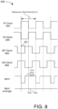
FIG. 8 shows a timing diagram of the input and output signals of the dual rail quadrature clock generation circuit ofFIG. 6A , according to some implementations. - In the following description, numerous specific details are set forth such as examples of specific components, circuits, and processes to provide a thorough understanding of the present disclosure. The term "coupled" as used herein means connected directly to or connected through one or more intervening components or circuits. The terms "electronic system" and "electronic device" may be used interchangeably to refer to any system capable of electronically processing information. Also, in the following description and for purposes of explanation, specific nomenclature is set forth to provide a thorough understanding of the aspects of the disclosure. However, it will be apparent to one skilled in the art that these specific details may not be required to practice the example implementations. In other instances, well-known circuits and devices are shown in block diagram form to avoid obscuring the present disclosure. Some portions of the detailed descriptions which follow are presented in terms of procedures, logic blocks, processing and other symbolic representations of operations on data bits within a computer memory.
- These descriptions and representations are the means used by those skilled in the data processing arts to most effectively convey the substance of their work to others skilled in the art. In the present disclosure, a procedure, logic block, process, or the like, is conceived to be a self-consistent sequence of steps or instructions leading to a desired result. The steps are those requiring physical manipulations of physical quantities. Usually, although not necessarily, these quantities take the form of electrical or magnetic signals capable of being stored, transferred, combined, compared, and otherwise manipulated in a computer system. It should be borne in mind, however, that all of these and similar terms are to be associated with the appropriate physical quantities and are merely convenient labels applied to these quantities.
- Unless specifically stated otherwise as apparent from the following discussions, it is appreciated that throughout the present disclosure, discussions utilizing the terms such as "accessing," "receiving," "sending," "using," "selecting," "determining," "normalizing," "multiplying," "averaging," "monitoring," "comparing," "applying," "updating," "measuring," "deriving" or the like, refer to the actions and processes of a computer system, or similar electronic computing device, that manipulates and transforms data represented as physical (electronic) quantities within the computer system's registers and memories into other data similarly represented as physical quantities within the computer system memories or registers or other such information storage, transmission or display devices.
- In the figures, a single block may be described as performing a function or functions; however, in actual practice, the function or functions performed by that block may be performed in a single component or across multiple components, and/or may be performed using hardware, using software, or using a combination of hardware and software. To clearly illustrate this interchangeability of hardware and software, various illustrative components, blocks, modules, circuits, and steps have been described below generally in terms of their functionality. Whether such functionality is implemented as hardware or software depends upon the particular application and design constraints imposed on the overall system. Skilled artisans may implement the described functionality in varying ways for each particular application, but such implementation decisions should not be interpreted as causing a departure from the scope of the present disclosure. Also, the example input devices may include components other than those shown, including well-known components such as a processor, memory and the like.
- The techniques described herein may be implemented in hardware, software, firmware, or any combination thereof, unless specifically described as being implemented in a specific manner. Any features described as modules or components may also be implemented together in an integrated logic device or separately as discrete but interoperable logic devices. If implemented in software, the techniques may be realized at least in part by a non-transitory processor-readable storage medium comprising instructions that, when executed, performs one or more of the methods described above. The non-transitory processor-readable data storage medium may form part of a computer program product, which may include packaging materials.
- Various implementations relate generally to the generation of quadrature clock signals. Some implementations more specifically relate to quadrature clock generators included in integrated circuits. In one implementation, an in-phase (I) clock generation circuit generates an I clock signal based on a reference clock signal, such as by delaying the reference clock signal. Thus, the I clock signal has the same frequency as the reference clock signal. A quadrature phase (Q) clock generation circuit generates a Q clock signal based on the reference clock signal, a rise time control signal, and a fall time control signal. The Q clock signal has the same frequency as the I clock signal (and the reference clock signal) but is offset in phase by 90 degrees with respect to the I clock signal. A control circuit generates the rise time control signal and the fall time control signal based on the I clock signal and the Q clock signal. The rise time control signal and the fall time control signal are used by the Q clock generation circuit in order to maintain the 90 degrees phase offset between the I clock signal and the Q clock signal and to maintain the proper 50% duty cycle for the Q clock signal.
- Particular implementations of the subject matter described in this disclosure can be implemented to realize one or more of the following potential advantages. In some implementations, rather than requiring a reference clock signal which is twice the frequency of the desired quadrature clock signals, as in some conventional clock generation circuits, the reference clock signal or signals required for the example implementations have the same frequency as the quadrature clock signals generated by the example circuits. This may result in reduced power consumption and heat generation. Further, the example implementations may generate the quadrature clock signals accurately, by determining the phase difference between the I and Q clock signals and correcting for phase mismatch by locking the delay to a 90 degree phase delay between the I and Q clock signals. Further, the example implementations may correct any duty cycle mismatches in the Q clock signals in order to ensure accurate clock signal generation for a wide variety of desired clock frequencies.
-
FIG. 1A shows a conventional digitalphase splitter circuit 100A, which may be used to generate quadrature clock signals. The digitalphase splitter circuit 100A may include a first flip-flop 120, a second flip-flop 130, and aninverter 140. Note that, while the first flip-flop 120 and second flip-flop 130 are shown as D flip-flops, other conventional digital phase splitter circuits may use other types of flip-flops or latches. - The first flip-
flop 120 may be clocked by areference clock signal 110, while an in-phase clock 150 may be generated at the output Q. The output Q_bar may be provided at the input D of the first flip-flop 120. Thereference clock 110 may be provided to theinverter 140, and the output of theinverter 140 is provided to the input D and the output Q_bar of the second flip-flop 130. Thequadrature phase clock 160 may be generated at the output Q_bar of the second flip-flop 130. As such, the in-phase clock 150 and the quadrature-phase clock 160 may each have a frequency which is half that of thereference clock 110. In other words, for a desired frequency of the clock signals 150 and 160, areference clock 110 having twice the frequency is required. -
FIG. 1B shows a timing diagram 100B of the input and output signals of the digitalphase splitter circuit 100A. Note that thereference clock 110 has twice the frequency of the in-phase clock 150 and twice the frequency of thequadrature phase clock 160. In other words, thereference clock period 111 is half of theoutput clock period 151. Additionally, note that the phase offset 161 between thequadrature phase clock 160 and the in-phase clock 150 is one quarter of theoutput clock period 161. -
FIG. 2 shows a conventional delay locked loop (DLL)circuit 200 for generating quadrature clock signals. TheDLL circuit 200 includes four delay cells 220(1)-220(4) (collectively delay cells 220). Each delay cell is configured to delay areference clock 210 by one quarter wavelength. For example, each delay cell of thedelay cells 220 may include an inverter and a capacitor, or another suitable circuit for delaying an input signal. Thus, at the output of the first delay cell 220(1), thereference clock 210 may be delayed by one quarter wavelength, or 90 degrees. The remaining delay stages may have identical structure, such that the second delay cell 220(2) outputs a signal corresponding to thereference clock 210 which has been delayed by one half wavelength, or 180 degrees. Similarly, the third delay call 220(3) outputs a signal corresponding to thereference clock 210 delayed by three quarters of a wavelength, or 270 degrees, and the fourth delay cell 220(4) outputs a signal which should be in phase with thereference clock 210. TheDLL circuit 200 outputs an in-phase clock 250, which may simply be thereference clock 210, and aquadrature phase clock 260, which may be the output of the first delay cell 220(1). - The
DLL circuit 200 also includes a delay lockedloop 230, which may receive thereference clock 210 and the output of the fourth delay cell 220(4) and generate delay control signals for thedelay cells 220. The delay lockedloop 230 may generate the delay control signals to correct for any mismatch between thereference clock 210 and the output of the delay cell 220(4), which should be identical and in phase with thereference clock 210. - While the digital
phase splitter circuit 100A and theDLL circuit 200 may be used to generate quadrature clock signals, they each have drawbacks. For example, the digitalphase splitter circuit 100A requires a reference clock signal having twice the frequency of the desired quadrature clock signals. This may result in undesirably high power consumption or circuit complexity for generating such high frequency reference clock signals. For example, chip to chip speeds are increasing due to the bandwidth needs of high-capacity network and high-performance computer systems, which may use high resolution video applications such as 4k and 8k. Further, interfaces may be required to support a variety of data rates as well, such as 5.4 Gbps, 6.75Gbps, 8.1 Gbps, 10 Gbps, 13.5 Gbps, 20Gbps, and so on, for backward compatibility and for low power consumption. Also, the digitalphase splitter circuit 100A cannot easily adjust for inaccurate duty cycles or phase offsets, which may result in inaccurate clock signals. - Use of the
DLL circuit 200 may result in aquadrature clock 260 having a distorted duty cycle, as the duty cycle is not controlled and may be distorted by thedelay cells 220 of theDLL circuit 200. Further, theDLL circuit 200 may experience harmonic locking issues, when the delay provided by the delay lockedloop 230 and thedelay cells 220 may not lock to one wavelength, but may lock to an integer N number of wavelengths. This may result in functional issues with theDLL circuit 200, or may require additional circuitry to avoid these harmonic locking issues. Further, thedelay cells 220 are difficult to match, and may not each provide precisely the same amount of delay, which may result in IQ phase delay errors due to this delay cell mismatch. - It would therefore be desirable to generate quadrature clock signals for a wide range of clock frequencies without requiring a double frequency reference clock, and which may accurately maintain required phase offset and duty cycle timing between the generated quadrature clock signals.
- The example implementations may generate quadrature clock signals using fully differential amplifier circuitry, and which may detect the phase difference between the in-phase (I) and quadrature phase (Q) clock signals using phase detection, and adjust the phase offset and duty cycle of the Q clock signals to maintain its desired quarter wavelength offset and 50% duty cycle.
-
FIG. 3 shows an examplequadrature clock generator 300, according to some implementations. Thequadrature clock generator 300 receives areference clock 302, which may optionally be buffered by abuffer 304. The bufferedreference clock 302 may be provided to an Iclock delay circuit 306 and one or more Q clock delay circuits 310(1)-310(N) (collectively Q clock delay circuits 310). The I clock delay circuit may delay thereference clock 302, generating anI clock 350 which may optionally be buffered by abuffer 308. ThisI clock 350 has the same frequency as thereference clock 302. The Qclock delay circuits 310 may each delay and adjust a phase offset and duty cycle of thereference clock 302 in order to generate theQ clock 360, which may optionally be buffered by abuffer 312. As with theI clock 350, theQ clock 360 also has the same frequency as thereference clock 302, but is shifted in phase by one quarter wavelength. Each Qclock delay circuit 310 may also receive a fall time control signal and a rise time control signal, which may be used by the Qclock delay circuits 310 to adjust the phase offset and duty cycles, as discussed in more detail below. - The fall time control signal and the rise time control signal may be generated by a control circuit including a
NAND gate 314, aresistor 316, acapacitor 318, adifferential amplifier 320,resistors amplifier 328, aresistor 330, and acapacitor 332. TheNAND gate 314 may receive theI clock 350 at a noninverting input, and theQ clock 360 at an inverting input, outputting an "iqout" signal, which may correspond to a phase difference between theI clock 350 and theQ clock 360. For example, when theI clock 350 and theQ clock 360 have the desired quarter wavelength, or 90 degree, phase difference, the iqout signal may have a 75% duty cycle. Note that in some aspects theNAND gate 314 may be replaced by a suitable IQ phase detect circuit, as described below. - The
resistor 316 andcapacitor 318 may generate an "iqout average" signal representing an average value of iqout. Thus, when theI clock 350 andQ clock 360 have proper phase difference of 90 degrees, iqout average has a value of 75% of a supply voltage of thequadrature clock generator 300, such as 75% of Vdd. Iqout average may be provided at a noninverting input of thedifferential amplifier 320. Theresistors differential amplifier 320. In this manner, the fall time control signal, provided from an inverting output of thedifferential amplifier 320, and the rise time control signal, provided from a noninverting output of thedifferential amplifier 320, may be based on the phase offset between theI clock 350 and theQ clock 360. - The
quadrature clock generator 300 may also provide duty cycle correction for theQ clock 360. For example, the output common mode voltage control for thedifferential amplifier 320 may be provided from an output of theamplifier 328. Theamplifier 328 has an inverting input coupled to receive a signal having a value of 50% of Vdd, corresponding to an intended 50% duty cycle of theQ clock 360. A noninverting input of theamplifier 328 may be coupled to receive a signal corresponding to an average value of theQ clock 360. This average value of theQ clock 360 may be generated from theQ clock 360 using theresistor 330 and thecapacitor 332. The output of theamplifier 328 controls rise time and fall time of Qclock delay circuits 310 by controlling the output common mode voltage of thedifferential amplifier 320 to adjustQ clock 360 duty cycle to 50% because the output of theamplifier 328 is based on a difference between the desired 50% duty cycle of Q clock 360-represented by the inverting input to the amplifier 328-and the actual duty cycle of the Q clock 360-represented by the noninverting input to theamplifier 328. - Note that while the averaging circuits in
FIG. 3 are shown as a resistor and a capacitor, such as theresistor 316 andcapacitor 318, that in other aspects other suitable circuits may be used for generating the average signal values. -
FIG. 4 shows an example Iclock delay circuit 400, which may be one example of the Iclock delay circuit 306 shown inFIG. 3 . The Iclock delay circuit 400 may include a simple inverter chain, such as including theinverters clock delay circuit 400 may also include acapacitor 420. Note that for higher frequency clocks, for example for 10 GHz clock, that a minimum delay for the Q clock delay circuits may be higher than the desired 90 degree phase difference between the I and Q clocks. Example quadrature clock generator circuits for such high frequency clocks may include an artificial delay added to the I clock delay circuits, such as the I clock delaycircuits -
FIG. 5 shows an example Qclock delay circuit 500, which may be one example of each of the Qclock delay circuits 310 ofFIG. 3 . The Qclock delay circuit 500 may receive the rise time control signal and the fall time control signal, such as from thedifferential amplifier 320. The Qclock delay circuit 500 may also receive an input, such as thereference clock 302, or an output from a previous Q clock delay circuit. This input signal may be provided to aninverter 510. A supply terminal of theinverter 510 may be coupled to a drain terminal of atransistor 520, which may be a P-channel metal-oxide-semiconductor (PMOS) transistor. A source terminal of thetransistor 520 may be coupled to a supply voltage, and a gate terminal of thetransistor 520 may be coupled to the rise time control signal. A ground terminal of theinverter 510 may be coupled to a drain terminal of atransistor 530, which may be an N-channel metal-oxide-semiconductor (NMOS) transistor. A source terminal of thetransistor 530 may be coupled to ground, and a gate terminal of thetransistor 530 may be coupled to the fall time control signal. An output of theinverter 510 may be coupled to thecapacitor 540 and theinverter 550. The output of theinverter 550 may be provided as the output of the Qclock delay circuit 500. - The Q clock delay cell may be controlled using the rise time control signal and fall time control signal. For example, when the rise time control signal increases, the rise time delay increases for the Q clock, due to the
transistor 520 becoming weaker. Similarly, when the rise time control signal decreases, the rise time delay decreases for the Q clock, as thetransistor 520 becomes stronger. As the fall time control signal increases, thetransistor 530 becomes stronger, and the fall time decreases for the Q clock. Similarly, when the fall time control signal decreases, the fall time delay increases for the Q clock. - In some aspects, the quadrature clock generators of the present disclosure may be provided for dual rail circuits. For example,
FIG. 6A shows an examplequadrature clock generator 600A for a dual rail quadrature clock generation circuit, according to some implementations. Rather than a single reference clock, as withFIG. 3 , a noninverted reference clock,P reference clock 602, and an inverted reference clock,N reference clock 604, may be provided to thequadrature clock generator 600A, optionally after being buffered byrespective buffers IP delay circuit 610, which may delay theP reference clock 602, and may include an inverter chain, such as with Iclock delay circuit 400. The output of theIP delay circuit 610 may, after optionally being buffered bybuffer 612, be provided as a noninverted I clock signal,IP clock 650. TheN reference clock 604 may be provided to INdelay circuit 614, which may delay theN reference clock 604, and may also include an inverter chain, such as with Iclock delay circuit 400. The output of theIN delay circuit 614 may, after optionally being buffered bybuffer 616, be provided as an inverted I clock signal, INclock 655. - The Q clocks, a
noninverted Q clock 660 and aninverted Q clock 665, may also be generated similarly toFIG. 3 . For example, theP reference clock 602 may be provided to one or more QP delay circuits 626(1)-626(N) (collectively QP delay circuits 626), each of which may receive a rise time control signal and a fall time control signal. After optionally being buffered bybuffer 628, the output of theQP delay circuits 626 may be provided as theQP clock 660. TheQP clock 660 may also be coupled to theresistor 630 and thecapacitor 632, and the signal at a node between theresistor 630 and thecapacitor 632 may be referred to as QP duty. Further, theN reference clock 604 may be provided to one or more QN delay circuits 634(1)-634(N) (collectively QN delay circuits 634), each of which may receive a rise time control signal and a fall time control signal. After optionally being buffered bybuffer 636, the output of theQN delay circuits 634 may be provided as theQN clock 665. TheQN clock 665 may also be coupled to theresistor 642 and thecapacitor 644, and the signal at a node between theresistor 642 and thecapacitor 644 may be referred to as QN duty. - Note that the
QP delay circuits 626 andQN delay circuits 634 may have the same structure as the Qclock delay circuits 310 or the Qclock delay circuit 500. - The separation of complementary rails, such as that of the
IP clock 650 and INclock 655, as well as of theQP clock 660 andQN clock 665, may be maintained using any suitable techniques, such as using the inverter pairs 618/620, 622/624, and 638/640. - The rise time control signal and fall time control signal may be generated similarly to the control circuit of
FIG. 3 .FIG. 6B shows anexample control circuit 600B for thequadrature clock generator 600A ofFIG. 6A . TheIP clock 650 and theQN clock 665 may be provided to aNAND gate 670, whose output is iqout. Similarly toFIG. 3 , iqout is averaged using aresistor 672 and acapacitor 674 and provided at a noninverting input to adifferential amplifier 676. An inverting input to thedifferential amplifier 676 may be a signal having a value corresponding to 75% of a supply voltage of thequadrature clock generator 600A. For example, this signal may be generated usingresistors differential amplifier 676 may be provided from an output of anamplifier 684. An inverting input of theamplifier 684 may be a signal having a value corresponding to 50% of Vdd, and a noninverting input of theamplifier 684 may be the signal QP duty shown inFIG. 6A . The rise time control signal and the fall time control signal may be the respective inverting and noninverting outputs of thedifferential amplifier 676. - While the iqout signal is shown in
FIG. 3 andFIG. 6B as being generated by a NAND gate, such theNAND gate 314 or theNAND gate 670, in some other aspects, iqout may be generated using an IQ phase detection circuit.FIG. 7 shows an example IQphase detection circuit 700 which may be used with the dual rail quadratureclock generation circuit 600A ofFIG. 6A , according to some implementations. A first pair oftransistors transistor 710 may have a source terminal coupled to Vdd, a gate terminal coupled to theQN clock 665, and a drain terminal coupled to iqout. Thetransistor 720 may have a drain terminal coupled to Vdd, a gate terminal coupled toQP clock 660, and a source terminal coupled to iqout. A second pair oftransistors transistor 730 may have a source terminal coupled to Vdd, a gate terminal coupled toIP clock 650, and a drain terminal coupled to iqout. Thetransistor 740 may have a drain terminal coupled to Vdd, a gate terminal coupled to INclock 655, and a source terminal coupled to iqout. - A third pair of
transistors transistors transistor 750 may have a source terminal coupled to iqout, a gate terminal coupled toIP clock 650, and a drain terminal coupled to a common node between the third pair oftransistors 750/760 and the fourth pair oftransistors 770/780. Thetransistor 760 may have a source terminal coupled to the common node between the third pair oftransistors 750/760 and the fourth pair oftransistors 770/780, a drain terminal coupled to iqout, and a gate terminal coupled to INclock 655. Thetransistor 770 may have a source terminal coupled to the common node, a gate terminal coupled toQN clock 665, and a drain terminal coupled to ground. Thetransistor 780 may have a drain terminal coupled to the common node, a gate terminal coupled toQP clock 660, and a source terminal coupled to ground. - Use of the IQ
phase detection circuit 700 shown inFIG. 7 rather than a NAND gate, such theNAND gate 314 or theNAND gate 670, may provide several advantages. For example, then the transistor sizes are the same, charge injection error may be reduced. Additionally, loading to all clocks may be identical, which may aid in matching the rise time and fall time of each clock. To reduce the variation between rise times and fall times of each clock, the sizes of pull-up network devices and pull-down network devices may be configured to match the rise time and fall time of the iqout signal. -
FIG. 8 shows a timing diagram 800 of the input and output signals of the dual rail quadratureclock generation circuit 600A ofFIG. 6A . As shown with respect toFIG. 8 , theIP clock 650 and INclock 655 are inverted but share a common reference clock frequency, shown by thereference clock period 810. Similarly, theQP clock 660 and theQN clock 665 share the same clock frequency andreference clock period 810, but are shifted in phase by a quarter wavelength, or 90 degrees, as shown by thephase difference 820. As described above, the iqout signal has a duty cycle of 75%, corresponding to the phase difference between the in phase clocksignals IP clock 650 and INclock 655 and the quadrature phase clock signalsQP clock 660 and ONclock 655. The iqout average signal, representing an averaged value of the iqout signal, has a value corresponding to 75% of Vdd. - Those of skill in the art will appreciate that information and signals may be represented using any of a variety of different technologies and techniques. For example, data, instructions, commands, information, signals, bits, symbols, and chips that may be referenced throughout the above description may be represented by voltages, currents, electromagnetic waves, magnetic fields or particles, optical fields or particles, or any combination thereof.
- In the foregoing specification, embodiments have been described with reference to specific examples thereof. It will, however, be evident that various modifications and changes may be made thereto without departing from the broader scope of the disclosure as set forth in the appended claims. The specification and drawings are, accordingly, to be regarded in an illustrative sense rather than a restrictive sense.
Claims (15)
- A quadrature clock generator, comprising:an in-phase (I) clock generation circuit to generate an I clock signal based on a reference clock signal, the I clock signal and the reference clock signal each having a first frequency;a quadrature phase (Q) clock generation circuit to generate a Q clock signal based on the reference clock signal, a rise time control signal, and a fall time control signal, the Q clock signal having the first frequency; anda control circuit to generate the rise time control signal and the fall time control signal based on the I clock signal and the Q clock signal.
- The quadrature clock generator of claim 1, wherein the I clock generation circuit comprises a delay circuit configured to delay the reference clock signal.
- The quadrature clock generator of claim 1 or claim 2, wherein the Q clock generation circuit comprises a plurality of Q clock delay cells, each Q clock delay cell coupled to the rise time control signal and the fall time control signal;
wherein, optionally, each Q clock delay cell comprises:a first inverter having an input terminal, a power terminal, a ground terminal, and an output terminal;a first transistor having a gate terminal coupled to the rise time control signal, a source terminal coupled to a supply voltage, and a drain terminal coupled to the power terminal of the first inverter; anda second transistor having a gate terminal coupled to the fall time control signal, a source terminal coupled to a ground voltage, and a drain terminal coupled to the ground terminal of the first inverter. - The quadrature clock generator of any one of the preceding claims, wherein the control circuit includes a differential amplifier comprising:a noninverting input terminal to receive an iqout average signal, the iqout average signal representing an average value of the I clock signal NAND an inverted Q clock signal;an inverting input terminal to receive a signal representing 75% of a supply voltage of the quadrature clock generator;a terminal to receive an output common mode voltage signal;an inverting output to provide the fall time control signal; anda noninverting output to provide the rise time control signal;wherein, optionally, the common mode signal is generated by an amplifier having an inverting input to receive a constant voltage signal representing 50% of the supply voltage, a noninverting input to receive a signal representing an average value of the Q clock signal, and an output terminal to provide the output common mode voltage signal.
- The quadrature clock generator of any one of the preceding claims, wherein the control circuit is further configured to determine the rise time control signal and the fall time control signal based at least in part on a difference between a duty cycle of the Q clock signal and 50% of a supply voltage of the quadrature clock generator.
- A quadrature clock generator, comprising:an in-phase (I) clock generation circuit to generate an I clock signal by delaying a reference clock signal, the I clock signal and the reference clock signal each having a first frequency;a quadrature phase (Q) clock generation circuit to generate a Q clock signal by delaying and adjusting a rise time and a fall time of the reference clock signal, the Q clock signal having the first frequency and having a phase offset of 90° with respect to the I clock signal; anda control circuit to determine a rise time control signal and a fall time control signal for adjusting the rise time and fall time of the Q clock signal based at least in part on the I clock signal and the Q clock signal.
- The quadrature clock generator of claim 6, wherein the Q clock generation circuit comprises a plurality of Q clock delay cells, each Q clock delay cell coupled to the rise time control signal and the fall time control signal.
- The quadrature clock generator of claim 6 or claim 7, wherein the rise time delay increases when the rise time control signal increases, and the rise time delay decreases when the rise time control signal decreases; and/or
wherein the fall time delay decreases when the fall time control signal increases, and the fall time delay increases when the fall time control signal decreases. - The quadrature clock generator of any one of claims 6 to 8,
wherein the control circuit is configured to determine the rise time control signal and the fall time control signal based at least in part on the phase offset between the I clock signal and the Q clock signal. - The quadrature clock generator of any one of claims 6 to 9,
wherein the control circuit is configured to determine the phase offset between the I clock signal and the Q clock signal based on a logic NAND between the I clock signal and an inverted Q clock signal. - The quadrature clock generator of any one of claims 6 to 10,
wherein the control circuit is further configured to determine the rise time control signal and the fall time control signal based at least in part on a difference between a duty cycle of the Q clock signal and 50% of a supply voltage of the quadrature clock generator. - A dual rail quadrature clock generator, comprising:an in-phase (I) clock generation circuit to generate a noninverted I clock signal and an inverted I clock signal based on a noninverted reference clock signal and an inverted reference clock signal, the noninverted I clock signal, the inverted I clock signal, the noninverted reference clock signal and the inverted reference clock signal each having a first frequency;a quadrature phase (Q) clock generation circuit to generate a noninverted Q clock signal and an inverted Q clock signal based on the noninverted reference clock signal, the inverted reference clock signal, the noninverted I clock signal, and the inverted Q clock signal, wherein the noninverted Q clock signal and the inverted Q clock signal have the first frequency; anda control circuit to generate a rise time control signal and a fall time control signal for adjusting a rise time and a fall time of the noninverted Q clock signal and the inverted Q clock signal, wherein the rise time control signal and the fall time control signal are generated based on the noninverted I clock signal and the inverted Q clock signal.
- The dual rail quadrature clock generator of claim 12, wherein the I clock generation circuit comprises a first I delay circuit configured to delay the noninverted reference clock signal to generate the noninverted I clock signal and a second I delay circuit configured to delay the inverted reference clock signal to generate the inverted I clock signal.
- The dual rail quadrature clock generator of claim 12 or claim 13, wherein the Q clock generation circuit comprises:a plurality of first Q clock delay cells, each first Q clock delay cell configured to receive the noninverted reference clock signal, the rise time control signal and the fall time control signal; anda plurality of second Q clock delay cells, each second Q clock delay cell configured to receive the inverted reference clock signal, the rise time control signal, and the fall time control signal;wherein, optionally, each first Q clock delay cell and each second Q clock delay cell comprises:a first inverter having an input terminal, a power terminal, a ground terminal, and an output terminal;a first transistor having a gate terminal coupled to the rise time control signal, a source terminal coupled to a supply voltage, and a drain terminal coupled to the power terminal of the first inverter; anda second transistor having a gate terminal coupled to the fall time control signal, a source terminal coupled to a ground voltage, and a drain terminal coupled to the ground terminal of the first inverter.
- The dual rail quadrature clock generator of any one of claims 12 to 14, wherein the control circuit includes a differential amplifier comprising:a noninverting input terminal to receive an iqout average signal, the iqout average signal representing an average value of the I clock signal NAND an inverted Q clock signal;an inverting input terminal to receive a signal representing 75% of a supply voltage;a terminal to receive an output common mode voltage signal;an inverting output to provide the fall time control signal; anda noninverting output to provide the rise time control signal;wherein, optionally, the output common mode voltage signal is generated by an amplifier having an inverting input to receive a constant voltage signal representing 50% of the supply voltage, a noninverting input to receive a signal representing an average value of the Q clock signal, and an output terminal to provide the output common mode voltage signal.
Applications Claiming Priority (2)
| Application Number | Priority Date | Filing Date | Title |
|---|---|---|---|
| US202263306408P | 2022-02-03 | 2022-02-03 | |
| US18/061,936 US12026009B2 (en) | 2022-02-03 | 2022-12-05 | Quadrature clock generator with duty cycle corrector |
Publications (1)
| Publication Number | Publication Date |
|---|---|
| EP4224711A1 true EP4224711A1 (en) | 2023-08-09 |
Family
ID=85150370
Family Applications (1)
| Application Number | Title | Priority Date | Filing Date |
|---|---|---|---|
| EP23154185.5A Pending EP4224711A1 (en) | 2022-02-03 | 2023-01-31 | Quadrature clock generator with duty cycle corrector |
Country Status (3)
| Country | Link |
|---|---|
| US (1) | US12026009B2 (en) |
| EP (1) | EP4224711A1 (en) |
| TW (1) | TW202333455A (en) |
Families Citing this family (2)
| Publication number | Priority date | Publication date | Assignee | Title |
|---|---|---|---|---|
| US20240283630A1 (en) * | 2023-02-16 | 2024-08-22 | Analog Devices, Inc. | Digital quadrature clock for low jitter applications |
| US12249989B1 (en) * | 2023-08-25 | 2025-03-11 | Realtek Semiconductor Corp. | Four-phase clock buffer of twenty-five percent duty cycle |
Citations (2)
| Publication number | Priority date | Publication date | Assignee | Title |
|---|---|---|---|---|
| WO2012100226A1 (en) * | 2011-01-21 | 2012-07-26 | Qualcomm Incorporated | System for i-q phase mismatch detection and correction |
| US20190123728A1 (en) * | 2017-10-19 | 2019-04-25 | Xilinx, Inc. | Quadrature clock correction circuit for transmitters |
Family Cites Families (2)
| Publication number | Priority date | Publication date | Assignee | Title |
|---|---|---|---|---|
| KR101036922B1 (en) * | 2008-04-11 | 2011-05-25 | 주식회사 하이닉스반도체 | Quadrature phase correction circuit |
| US9897686B2 (en) * | 2013-02-12 | 2018-02-20 | Nxp Usa, Inc. | Active IQ and quadrature generator for high frequency applications |
-
2022
- 2022-12-05 US US18/061,936 patent/US12026009B2/en active Active
-
2023
- 2023-01-31 EP EP23154185.5A patent/EP4224711A1/en active Pending
- 2023-02-02 TW TW112103668A patent/TW202333455A/en unknown
Patent Citations (2)
| Publication number | Priority date | Publication date | Assignee | Title |
|---|---|---|---|---|
| WO2012100226A1 (en) * | 2011-01-21 | 2012-07-26 | Qualcomm Incorporated | System for i-q phase mismatch detection and correction |
| US20190123728A1 (en) * | 2017-10-19 | 2019-04-25 | Xilinx, Inc. | Quadrature clock correction circuit for transmitters |
Also Published As
| Publication number | Publication date |
|---|---|
| TW202333455A (en) | 2023-08-16 |
| US12026009B2 (en) | 2024-07-02 |
| US20230244266A1 (en) | 2023-08-03 |
Similar Documents
| Publication | Publication Date | Title |
|---|---|---|
| US9571106B2 (en) | Delay locked loop circuit | |
| US8854098B2 (en) | System for I-Q phase mismatch detection and correction | |
| US10044359B1 (en) | Injection locked phase locked loop | |
| US8008954B2 (en) | Multi-phase signal generator and method | |
| EP4224711A1 (en) | Quadrature clock generator with duty cycle corrector | |
| US9048820B2 (en) | High-speed fully-differential clock duty cycle calibration circuit | |
| Chae et al. | A quadrature clock corrector for DRAM interfaces, with a duty-cycle and quadrature phase detector based on a relaxation oscillator | |
| US10784847B1 (en) | Duty cycle correction circuit | |
| US20140035636A1 (en) | Clock synchronization circuit | |
| US7683683B1 (en) | Frequency doubler with duty-cycle correction and associated methods | |
| US11424735B2 (en) | Duty correction device and method, and semiconductor apparatus using the same | |
| US11456749B2 (en) | Timing margin detecting circuit, timing margin detecting method and clock and data recovery system | |
| US10848297B1 (en) | Quadrature clock skew calibration circuit | |
| CN111835346B (en) | Clock data recovery circuit | |
| EP4550666A1 (en) | Method and system for injection locked divider with frequency calibration | |
| US7330059B2 (en) | In-loop duty corrector delay-locked loop for multiphase clock generation | |
| US9698808B1 (en) | Phase measurement and correction circuitry | |
| US11057039B1 (en) | Clock divider with quadrature error correction | |
| US7593497B2 (en) | Method and apparatus for adjustment of synchronous clock signals | |
| US6529571B1 (en) | Method and apparatus for equalizing propagation delay | |
| US9329609B1 (en) | Feedback based topology for synchronization of multi-voltage domain signals in differential drivers | |
| Ko et al. | A 3.2-GHz quadrature error corrector for DRAM transmitters, using replica serializers and pulse-shrinking delay lines | |
| CN116545416A (en) | Quadrature Clock Generator with Duty Cycle Corrector | |
| US11581877B1 (en) | Negative-feedback four-phase generator with twenty-five percent duty cycle output | |
| US8970273B2 (en) | Phase offset cancellation circuit and associated clock generator |
Legal Events
| Date | Code | Title | Description |
|---|---|---|---|
| PUAI | Public reference made under article 153(3) epc to a published international application that has entered the european phase |
Free format text: ORIGINAL CODE: 0009012 |
|
| STAA | Information on the status of an ep patent application or granted ep patent |
Free format text: STATUS: THE APPLICATION HAS BEEN PUBLISHED |
|
| AK | Designated contracting states |
Kind code of ref document: A1 Designated state(s): AL AT BE BG CH CY CZ DE DK EE ES FI FR GB GR HR HU IE IS IT LI LT LU LV MC ME MK MT NL NO PL PT RO RS SE SI SK SM TR |
|
| STAA | Information on the status of an ep patent application or granted ep patent |
Free format text: STATUS: REQUEST FOR EXAMINATION WAS MADE |
|
| P01 | Opt-out of the competence of the unified patent court (upc) registered |
Effective date: 20240104 |
|
| 17P | Request for examination filed |
Effective date: 20240118 |
|
| RBV | Designated contracting states (corrected) |
Designated state(s): AL AT BE BG CH CY CZ DE DK EE ES FI FR GB GR HR HU IE IS IT LI LT LU LV MC ME MK MT NL NO PL PT RO RS SE SI SK SM TR |