EP4220953A1 - Driving amplifier stage with low output impedance - Google Patents
Driving amplifier stage with low output impedance Download PDFInfo
- Publication number
- EP4220953A1 EP4220953A1 EP23153991.7A EP23153991A EP4220953A1 EP 4220953 A1 EP4220953 A1 EP 4220953A1 EP 23153991 A EP23153991 A EP 23153991A EP 4220953 A1 EP4220953 A1 EP 4220953A1
- Authority
- EP
- European Patent Office
- Prior art keywords
- amplifier
- stack
- coupled
- voltage supply
- amplifier stage
- Prior art date
- Legal status (The legal status is an assumption and is not a legal conclusion. Google has not performed a legal analysis and makes no representation as to the accuracy of the status listed.)
- Pending
Links
- 230000000295 complement effect Effects 0.000 claims abstract description 9
- 230000005669 field effect Effects 0.000 claims abstract description 9
- 229910044991 metal oxide Inorganic materials 0.000 claims abstract description 7
- 150000004706 metal oxides Chemical class 0.000 claims abstract description 7
- 239000004065 semiconductor Substances 0.000 claims abstract description 7
- 239000003990 capacitor Substances 0.000 claims description 28
- 230000009466 transformation Effects 0.000 claims description 6
- 230000005540 biological transmission Effects 0.000 abstract description 10
- 238000010586 diagram Methods 0.000 description 14
- 230000008878 coupling Effects 0.000 description 4
- 238000010168 coupling process Methods 0.000 description 4
- 238000005859 coupling reaction Methods 0.000 description 4
- 230000008030 elimination Effects 0.000 description 4
- 238000003379 elimination reaction Methods 0.000 description 4
- 238000010295 mobile communication Methods 0.000 description 4
- 230000008901 benefit Effects 0.000 description 3
- 238000000034 method Methods 0.000 description 3
- 230000008569 process Effects 0.000 description 3
- 230000001413 cellular effect Effects 0.000 description 2
- 238000004891 communication Methods 0.000 description 2
- 238000013461 design Methods 0.000 description 2
- 238000001914 filtration Methods 0.000 description 2
- 230000006870 function Effects 0.000 description 2
- 230000009467 reduction Effects 0.000 description 2
- 239000000758 substrate Substances 0.000 description 2
- 230000007704 transition Effects 0.000 description 2
- 230000003321 amplification Effects 0.000 description 1
- 238000013459 approach Methods 0.000 description 1
- 230000003750 conditioning effect Effects 0.000 description 1
- 230000001419 dependent effect Effects 0.000 description 1
- 238000011161 development Methods 0.000 description 1
- 238000005516 engineering process Methods 0.000 description 1
- 229910052732 germanium Inorganic materials 0.000 description 1
- GNPVGFCGXDBREM-UHFFFAOYSA-N germanium atom Chemical compound [Ge] GNPVGFCGXDBREM-UHFFFAOYSA-N 0.000 description 1
- 230000036541 health Effects 0.000 description 1
- 230000006872 improvement Effects 0.000 description 1
- 230000000977 initiatory effect Effects 0.000 description 1
- 239000012212 insulator Substances 0.000 description 1
- 239000000463 material Substances 0.000 description 1
- 238000012986 modification Methods 0.000 description 1
- 230000004048 modification Effects 0.000 description 1
- 238000003199 nucleic acid amplification method Methods 0.000 description 1
- 238000012545 processing Methods 0.000 description 1
- 230000008054 signal transmission Effects 0.000 description 1
- 229910052710 silicon Inorganic materials 0.000 description 1
- 239000010703 silicon Substances 0.000 description 1
Images





Classifications
-
- H—ELECTRICITY
- H03—ELECTRONIC CIRCUITRY
- H03F—AMPLIFIERS
- H03F3/00—Amplifiers with only discharge tubes or only semiconductor devices as amplifying elements
- H03F3/20—Power amplifiers, e.g. Class B amplifiers, Class C amplifiers
- H03F3/24—Power amplifiers, e.g. Class B amplifiers, Class C amplifiers of transmitter output stages
- H03F3/245—Power amplifiers, e.g. Class B amplifiers, Class C amplifiers of transmitter output stages with semiconductor devices only
-
- H—ELECTRICITY
- H03—ELECTRONIC CIRCUITRY
- H03F—AMPLIFIERS
- H03F3/00—Amplifiers with only discharge tubes or only semiconductor devices as amplifying elements
- H03F3/20—Power amplifiers, e.g. Class B amplifiers, Class C amplifiers
- H03F3/21—Power amplifiers, e.g. Class B amplifiers, Class C amplifiers with semiconductor devices only
- H03F3/217—Class D power amplifiers; Switching amplifiers
-
- H—ELECTRICITY
- H03—ELECTRONIC CIRCUITRY
- H03F—AMPLIFIERS
- H03F3/00—Amplifiers with only discharge tubes or only semiconductor devices as amplifying elements
- H03F3/189—High-frequency amplifiers, e.g. radio frequency amplifiers
- H03F3/19—High-frequency amplifiers, e.g. radio frequency amplifiers with semiconductor devices only
- H03F3/195—High-frequency amplifiers, e.g. radio frequency amplifiers with semiconductor devices only in integrated circuits
-
- H—ELECTRICITY
- H03—ELECTRONIC CIRCUITRY
- H03F—AMPLIFIERS
- H03F1/00—Details of amplifiers with only discharge tubes, only semiconductor devices or only unspecified devices as amplifying elements
- H03F1/02—Modifications of amplifiers to raise the efficiency, e.g. gliding Class A stages, use of an auxiliary oscillation
- H03F1/0205—Modifications of amplifiers to raise the efficiency, e.g. gliding Class A stages, use of an auxiliary oscillation in transistor amplifiers
- H03F1/0211—Modifications of amplifiers to raise the efficiency, e.g. gliding Class A stages, use of an auxiliary oscillation in transistor amplifiers with control of the supply voltage or current
- H03F1/0216—Continuous control
- H03F1/0222—Continuous control by using a signal derived from the input signal
-
- H—ELECTRICITY
- H03—ELECTRONIC CIRCUITRY
- H03F—AMPLIFIERS
- H03F1/00—Details of amplifiers with only discharge tubes, only semiconductor devices or only unspecified devices as amplifying elements
- H03F1/56—Modifications of input or output impedances, not otherwise provided for
-
- H—ELECTRICITY
- H03—ELECTRONIC CIRCUITRY
- H03F—AMPLIFIERS
- H03F3/00—Amplifiers with only discharge tubes or only semiconductor devices as amplifying elements
- H03F3/20—Power amplifiers, e.g. Class B amplifiers, Class C amplifiers
- H03F3/24—Power amplifiers, e.g. Class B amplifiers, Class C amplifiers of transmitter output stages
-
- H—ELECTRICITY
- H03—ELECTRONIC CIRCUITRY
- H03F—AMPLIFIERS
- H03F3/00—Amplifiers with only discharge tubes or only semiconductor devices as amplifying elements
- H03F3/30—Single-ended push-pull [SEPP] amplifiers; Phase-splitters therefor
- H03F3/3001—Single-ended push-pull [SEPP] amplifiers; Phase-splitters therefor with field-effect transistors
- H03F3/3022—CMOS common source output SEPP amplifiers
-
- H—ELECTRICITY
- H03—ELECTRONIC CIRCUITRY
- H03F—AMPLIFIERS
- H03F3/00—Amplifiers with only discharge tubes or only semiconductor devices as amplifying elements
- H03F3/45—Differential amplifiers
- H03F3/45071—Differential amplifiers with semiconductor devices only
- H03F3/45076—Differential amplifiers with semiconductor devices only characterised by the way of implementation of the active amplifying circuit in the differential amplifier
- H03F3/45179—Differential amplifiers with semiconductor devices only characterised by the way of implementation of the active amplifying circuit in the differential amplifier using MOSFET transistors as the active amplifying circuit
-
- H—ELECTRICITY
- H03—ELECTRONIC CIRCUITRY
- H03F—AMPLIFIERS
- H03F3/00—Amplifiers with only discharge tubes or only semiconductor devices as amplifying elements
- H03F3/45—Differential amplifiers
- H03F3/45071—Differential amplifiers with semiconductor devices only
- H03F3/45076—Differential amplifiers with semiconductor devices only characterised by the way of implementation of the active amplifying circuit in the differential amplifier
- H03F3/45475—Differential amplifiers with semiconductor devices only characterised by the way of implementation of the active amplifying circuit in the differential amplifier using IC blocks as the active amplifying circuit
-
- H—ELECTRICITY
- H03—ELECTRONIC CIRCUITRY
- H03F—AMPLIFIERS
- H03F2200/00—Indexing scheme relating to amplifiers
- H03F2200/411—Indexing scheme relating to amplifiers the output amplifying stage of an amplifier comprising two power stages
-
- H—ELECTRICITY
- H03—ELECTRONIC CIRCUITRY
- H03F—AMPLIFIERS
- H03F2200/00—Indexing scheme relating to amplifiers
- H03F2200/451—Indexing scheme relating to amplifiers the amplifier being a radio frequency amplifier
-
- H—ELECTRICITY
- H03—ELECTRONIC CIRCUITRY
- H03F—AMPLIFIERS
- H03F2203/00—Indexing scheme relating to amplifiers with only discharge tubes or only semiconductor devices as amplifying elements covered by H03F3/00
- H03F2203/30—Indexing scheme relating to single-ended push-pull [SEPP]; Phase-splitters therefor
- H03F2203/30084—Indexing scheme relating to single-ended push-pull [SEPP]; Phase-splitters therefor the pull circuit of the SEPP amplifier being a cascode circuit
-
- H—ELECTRICITY
- H03—ELECTRONIC CIRCUITRY
- H03F—AMPLIFIERS
- H03F2203/00—Indexing scheme relating to amplifiers with only discharge tubes or only semiconductor devices as amplifying elements covered by H03F3/00
- H03F2203/30—Indexing scheme relating to single-ended push-pull [SEPP]; Phase-splitters therefor
- H03F2203/30105—Indexing scheme relating to single-ended push-pull [SEPP]; Phase-splitters therefor the pull transistor of the asymmetrically driven SEPP amplifier being a driven current mirror
-
- H—ELECTRICITY
- H03—ELECTRONIC CIRCUITRY
- H03F—AMPLIFIERS
- H03F2203/00—Indexing scheme relating to amplifiers with only discharge tubes or only semiconductor devices as amplifying elements covered by H03F3/00
- H03F2203/30—Indexing scheme relating to single-ended push-pull [SEPP]; Phase-splitters therefor
- H03F2203/30117—Indexing scheme relating to single-ended push-pull [SEPP]; Phase-splitters therefor the push circuit of the SEPP amplifier being a cascode circuit
-
- H—ELECTRICITY
- H03—ELECTRONIC CIRCUITRY
- H03F—AMPLIFIERS
- H03F2203/00—Indexing scheme relating to amplifiers with only discharge tubes or only semiconductor devices as amplifying elements covered by H03F3/00
- H03F2203/30—Indexing scheme relating to single-ended push-pull [SEPP]; Phase-splitters therefor
- H03F2203/30138—Indexing scheme relating to single-ended push-pull [SEPP]; Phase-splitters therefor the push transistor of the asymmetrically driven SEPP amplifier being a driven current mirror
Definitions
- the technology of the disclosure relates generally to a driving circuit for a power amplifier.
- CMOS complementary metal oxide semiconductor
- a driving amplifier stage comprises an input.
- the driving amplifier stage also comprises an output.
- the driving amplifier stage also comprises an amplifier stack coupled to the input.
- the amplifier stack comprises a first amplifier coupled to the input and the output.
- the amplifier stack also comprises a second amplifier coupled to the input and coupled to the output such that a summed output signal is available at the output.
- the amplifier stack also comprises a voltage supply input.
- the amplifier stack also comprises a mid-level voltage supply input node between the first amplifier and the second amplifier. The mid-level voltage supply input node is configured to be held at a fraction of a voltage supply level to limit voltage swing across the first amplifier.
- a driving amplifier stage comprises an input configured to receive a radio frequency (RF) input.
- the driving amplifier stage also comprises an amplifier stack.
- the amplifier stack comprises a first amplifier comprising a CMOS arrangement of a first n-type FET (NFET) and a first p-type FET (PFET).
- the amplifier stack also comprises a mid-level voltage supply input node coupled to the first amplifier.
- the amplifier stack also comprises a second amplifier comprising a CMOS arrangement of a second NFET and a second PFET.
- the second PFET is coupled to the mid-level voltage supply input node.
- the first amplifier and the second amplifier share a current.
- the amplifier stack also comprises an output configured to provide a summed output signal from the first amplifier and the second amplifier.
- an amplifier system comprising a driving amplifier stage.
- the driving amplifier stage comprises an input configured to receive an RF input.
- the driving amplifier stage also comprises an amplifier stack.
- the amplifier stack comprises a first amplifier comprising a CMOS arrangement of a first NFET and a first PFET.
- the amplifier stack also comprises a mid-level voltage supply input node coupled to the first amplifier.
- the amplifier stack also comprises a second amplifier comprising a CMOS arrangement of a second NFET and a second PFET.
- the second PFET is coupled to the mid-level voltage supply input node.
- the first amplifier and the second amplifier share a current.
- the amplifier system also comprises an output power amplifier stage coupled to the output.
- aspects disclosed in the detailed description include a driving amplifier stage with low output impedance.
- example aspects of the present disclosure contemplate a driving amplifier stage that does not need an inter-stage impedance matching network between the driving amplifier stage and an output amplifier stage in a transmission chain.
- the low output impedance of the driving amplifier stage may be achieved by providing stacking transconductance devices within the driving amplifier stage and reusing a supply current to provide an intermediate signal with high current but moderated voltage swing to drive the output amplifier stage.
- the stacked transconductance devices may be complementary metal oxide semiconductor (CMOS) field effect transistors (FETs). By providing a high current intermediate signal with moderate voltage swing, the need for an interstage matching circuit may be reduced or eliminated.
- CMOS complementary metal oxide semiconductor
- FIG. 1 is a block diagram of a transmission chain 100 of a mobile computing device (not shown).
- a baseband signal containing information to be transmitted may be generated by a baseband processor (not shown) and converted to a frequency of interest (e.g., frequencies complying with the 5G-NR standard or other radio frequency (RF).
- This RF signal is provided to a driving amplifier stage 102.
- the driving amplifier stage 102 may be a FET, a bipolar junction transistor (BJT), or a heterojunction bipolar transistor (HBT).
- BJT bipolar junction transistor
- HBT heterojunction bipolar transistor
- the driving amplifier stage 102 receives a low current (Low 1) from a voltage source (not shown) and outputs a large swing voltage signal 104 at output 106 as a function of the relatively high impedance of the driving amplifier stage 102.
- An output amplifier stage 108 is used to boost the signal to levels suitable for transmission and generally has a low impedance input 110, but takes a relatively high current (High 1) from a voltage source.
- the low impedance input 110 is configured to receive a relatively low swing voltage signal 112.
- an inter-stage step-down impedance network or circuit 114 is used to transform the signal as desired.
- inter-stage step-down impedance circuit 114 imposes a physical cost in terms of space and bill of materials. For example, at the frequencies of interest, such a circuit is likely a higher order circuit with a relatively large inductor. Alternatively, such inter-stage step-down impedance circuit 114 may impose severe bandwidth limitations, which are not desirable. Additionally, the presence of the inter-stage step-down impedance circuit 114 may consume power and attenuate the signal to be transmitted by some amount, requiring extra amplification by the output amplifier stage 108.
- Example aspects of the present disclosure provide an improved driving amplifier stage that allows the simplification or elimination of the inter-stage step-down impedance circuit 114.
- example aspects of the present disclosure provide a driving amplifier stage that has a reduced output impedance.
- the reduced output impedance is achieved by providing stacked transconductance devices.
- the stacked transconductance devices use a stacked complementary amplifier configuration that provides a large stage gain by using a current reuse configuration.
- Elimination of the inter-stage step-down impedance circuit 114 further allows for the signal path to the output amplifier stage to be wide bandwidth, which is important at the frequencies of interest. It should be appreciated that while elimination of the inter-stage step-down impedance circuit 114 is desired, some alternating current (AC) coupling and/or optional high-pass filters may remain in place to assist in conditioning the signal for use by the output amplifier stage.
- AC alternating current
- the transmission chain 200 may include a baseband processor (not shown) and an intermediate frequency processor (also not shown) that generates an RF signal that is provided to a driving amplifier stage 202.
- the driving amplifier stage 202 receives a low current (Low I) from a voltage source (not shown) and outputs a low swing voltage signal 204 at output 206.
- An output amplifier stage 208 is used to boost the signal to levels suitable for transmission and generally has a low impedance input 210, but takes a relatively high current (High I) from a voltage source.
- the low impedance input 210 is configured to receive the relatively low swing voltage signal 204.
- the inter-stage matching circuitry is eliminated.
- some AC coupling and optional high-pass filtering may be kept as some form of inter-stage network. However, such minimal circuitry should not hamper the signal path bandwidth.
- the driving amplifier stage 202 may be formed from stacked amplifiers that use an AC input split and output combining. Two examples of driving amplifier stages are provided in Figures 3A and 3B .
- Figure 3A illustrates a driving amplifier stage 300 having two stacked amplifiers 302, 304.
- the two stacked amplifiers 302, 304 may be coupled to an input 306 through capacitors 308, 310 and coupled to an output 312 (analogous to output 206) through capacitors 314, 316.
- the amplifier 302 may be coupled to a voltage source 318 (VDD) and may be an inverting or non-inverting amplifier.
- VDD voltage source 318
- the two stacked amplifiers 302, 304 are joined at a node 320, which may also be coupled to a voltage source 322 (mid-level voltage supply), which may be VDD/2 or the like as better explained below. Accordingly, the node 320 may be referred to as a mid-level voltage supply input node which is configured to be held at a fraction of a voltage supply level to limit voltage swing across the amplifier 302.
- the amplifier 304 may be coupled to the voltage source 322 and to a reference voltage 324, which may be VSS or a ground.
- Figure 3B illustrates a driving amplifier stage 350 having three stacked amplifiers 352, 354, 356.
- the three stacked amplifiers 352, 354, 356 may be coupled to an input 358 through capacitors 360, 362, 364 and coupled to an output 366 (analogous to output 206) through capacitors 368, 370, 372.
- the amplifier 352 may be coupled to a voltage source 374 (VDD) and may be an inverting or non-inverting amplifier.
- the amplifiers 352, 354 are joined at a node 376, which may also be coupled to a voltage source 378 (Vsup1), which may be 2VDD/3, or the like as better explained below.
- VDD voltage source 374
- Vsup1 voltage source 378
- the amplifiers 354, 356 are joined at a node 380, which may also be coupled to a voltage source 382 (Vsup2), which may be VDD/3 or the like as better explained below.
- Vsup2 voltage source 382
- the amplifier 356 may be coupled to the voltage source 382 and to a reference voltage 384, which may be VSS or a ground.
- Figure 4 provides more details about the stacked amplifiers of Figures 3A as well as one possible way that mid-level voltage supply may be provided.
- the power amplifiers 302 and 304 may not only be stacked relative to one another, but also contain stacked complementary FETs therewithin.
- the power amplifier 302 may include a p-type FET (PFET) 400 and an n-type FET (NFET) 402
- the power amplifier 304 may include a PFET 404 and an NFET 406.
- the capacitor 308 may include parallel capacitors 410, 412
- the capacitor 310 may include parallel capacitors 414, 416.
- the original voltage source 318 may be supplied to a supply voltage divider 418, which charges a capacitor 420 that may act as a filtering capacitance to provide an AC/RF supply current Iac to the node 320.
- VDD/2 i.e., half or a fraction of the voltage source 3128
- the rail-to-rail voltage swing of the amplifier 302 or 304 is limited to VDD/2 while the current is shared across the amplifiers 302, 304 and doubled through transconductance stacking.
- CMOS processes e.g., silicon on insulator (SOI) CMOS processes
- SOI silicon on insulator
- strained PFETs e.g., Germanium (Ge) strained
- the comparable FETs 400, 402, 404, 406 allows the FETs 400, 402, 404, 406 to be stacked without bringing a capacitance drawback, and the same transconductance gain per capacitance is achieved by the PFETs 400, 404 and the NFETs 402, 406.
- the net result of the transconductance stacking of the FETs 400, 402, 404, 406 is a four-fold reduction in impedance level at the output 312. It should be appreciated that a larger number of stacked CMOS stages can be placed on top of each other. Thus, for example, if the same stacking is applied to the driving amplifier stage 350 of Figure 3B , with Vsup1 being 2VDD/3 and Vsup2 being VDD/3, a nine-fold impedance reduction may be achieved. Accordingly, given a specific input impedance for an output amplifier stage 208, an appropriate stack size may be chosen to have a comparable impedance level, and thus avoid the need of a band limiting inter-stage step-down impedance circuit 114.
- the battery supply is set for 3.4 volts (V), and thus, it may be possible to bias the driving amplifier stage 350 directly from the battery since the FETs are designed for 1.2 V supply. That is, each of the paired stacks has a swing of one-third of the battery level, which is less than the designed 1.2 V.
- Figure 5 provides additional details about example biasing circuitry.
- a signal arrives at the input 306 and passes through the capacitors 410, 412, 414, 416 to the FETs 400, 402, 404, 406 and particularly to respective gates of the FETs 400, 402, 404, 406.
- the gate 404G is also connected to a bias circuit 500 through a resistor 502.
- the gate 406G is also connected to the bias circuit 500 through a resistor 504.
- the bias circuit 500 may be coupled to the ground 324.
- the voltage supply 318 may be coupled to a source 400S. Additionally, the voltage supply 318 may be coupled to a source 506S of a PFET 506.
- a gate 506G may be coupled to a node 508.
- the node 508 is coupled to the voltage source 318 through a capacitor 510.
- the node 508 is coupled to a gate 400G through a resistor 512.
- a drain 506D may be coupled to a drain 514D of a transistor 514.
- a source 514S may be coupled to the bias circuit 500.
- a gate 514G may be coupled to a node 516.
- the node 516 is coupled to a gate 402G through a resistor 518.
- the node 516 may be coupled to the node 320 through a capacitor 520. It should be appreciated that other bias circuits and bias networks may be used.
- the output amplifier stage 208 of Figure 5 is single-ended and unipolar.
- the present disclosure is not so limited, and as illustrated in Figure 6 , a differential input output amplifier stage 208D may be used with a driving amplifier stage 600.
- the driving amplifier stage 600 is substantially similar to the driving amplifier stage 300 illustrated in Figure 5 .
- Two additional capacitors 602, 604 are added, coupling the output amplifier stage 208D to the common drain nodes 606, 608, respectively.
- the output amplifier stage 208D may also be stacked transconductance devices as illustrated in Figure 7 .
- the output amplifier stage 208D may include FETs 700, 702, 704, 706 coupled at gates 700G, 706G to the driving amplifier stage 300 previously described.
- the FETs 700, 702 may be PFETs and the FETS 704, 706 may be NFETs.
- Collectively the FETs 700, 702, 704, 706 provide a stacked transconductance.
- Figure 8 provides a similar expansion of the driving amplifier stage 350 coupled to an output amplifier stage 800.
- the output amplifier stage 800 may include stacked FETs 802, 804, 806, which may be PFETs and FETs 808, 810, 812, which may be NFETs.
- the amplifier 352 may be a stacked PFET 814 and NFET 816.
- the amplifier 354 may be a stacked PFET 818 and NFET 820.
- the amplifier 356 may be a stacked PFET 822 and NFET 824.
- capacitors 826, 828, 830 may couple the amplifiers 352, 354, 356 to the output amplifier stage 800.
- Bias circuits 832, 834, 836 may be used to provide bias to the amplifiers 352, 354, 356 through the capacitors and resistors noted similar to those described above in Figure 5 . Again, the three stacked amplifiers 352, 354, 356 reuse the same supply current and have the voltage swing reduced through the use of the intermediate supply voltages Vsup1, Vsup2.
- Figure 9 provides an example of a completely differential driving amplifier stage 900 coupled to a differential-to-single-ended output amplifier stage 208D.
- the driving amplifier stage 900 includes differential inputs 902(1), 902(2) and differential outputs 904(1), 904(2).
- the input 902(1) and output 904(1) are associated with stacked transconductance devices, namely amplifiers 906, 908, which may be analogous to amplifiers 302, 304, respectively.
- the input 902(2) and output 904(2) are associated with stacked transconductance devices 910, 912, which may be analogous to amplifiers 302, 304, respectively.
- AC coupling capacitors 914, 916, 918, 920, 922, 924, 926, 928 may be used as previously described.
- capacitors used to support the mid voltage supplies are typically going to be fairly large. While a single such capacitor 420 may be an acceptable design compromise for two stacked amplifiers 302, 304, such approach may consume too much real estate when expanded to more than two stacked amplifiers.
- driving amplifier stage 1000 in Figure 10 that has three stacked amplifiers 1002, 1004, 1006, two large capacitors 1008 and 1010 are used to supply mid voltages 2VDD/3 and VDD/3. The more stacked amplifiers present in a driving amplifier stage, the more real estate that is consumed.
- Example aspects of the present disclosure provide an alternate solution to the large capacitors 1008, 1010 that is well suited for use in differential or quadrature structures as shown in Figures 11 and 12 .
- a mirrored arrangement is provided which allows for current to be reused between branches of the mirrored arrangement.
- Figure 11 illustrates a differential driving amplifier stage 1100 with a first stack 1102 and a second stack 1104.
- the first stack 1102 includes three stacked amplifiers 1106, 1108, 1110.
- the second stack 1104 includes three stacked amplifiers 1112, 1114, 1116.
- Node 1118 exists between amplifiers 1106 and 1108, and node 1120 exists between amplifiers 1108 and 1110.
- the nodes 1118 and 1120 correspond to the input nodes for the mid-level voltage supplies.
- node 1122 exists between amplifiers 1112 and 1114, and node 1124 exists between amplifiers 1114 and 1116.
- the node 1118 is coupled to the node 1122, and the node 1120 is coupled to the node 1124.
- This arrangement allows current to be provided from the node 1122 to the node 1118 and vice versa depending on changes in the supply provided to the different stacks 1102, 1104. Likewise, current may be provided from the node 1124 to the node 1120 and vice versa. While there may be more devices in the driving amplifier stage 1100 compared to the driving amplifier stage 1000, the overall size may be reduced because of the elimination of the capacitors 1008, 1110.
- the driving amplifier stage 1200 includes stacks 1202, 1204, 1206, 1208 which are coupled at nodes 1210, 1212, 1214, 1216 and also at nodes 1218, 1220, 1222, 1224. Again, current can flow between the nodes as needed to provide the appropriate supply voltage without the need for large bypass capacitors.
- the driving amplifier stage with low output impedance may be provided in or integrated into any processor-based device.
- Examples include a set top box, an entertainment unit, a navigation device, a communications device, a fixed location data unit, a mobile location data unit, a global positioning system (GPS) device, a mobile phone, a cellular phone, a smart phone, a session initiation protocol (SIP) phone, a tablet, a phablet, a server, a computer, a portable computer, a mobile computing device, a wearable computing device (e.g., a smart watch, a health or fitness tracker, eyewear, etc.), a desktop computer, a personal digital assistant (PDA), a monitor, a computer monitor, a television, a tuner, a radio, a satellite radio, a music player, a digital music player, a portable music player, a digital video player, a video player, a digital video disc (DVD) player, a portable digital video player
- GPS global positioning system
Landscapes
- Engineering & Computer Science (AREA)
- Power Engineering (AREA)
- Microelectronics & Electronic Packaging (AREA)
- Amplifiers (AREA)
Abstract
Description
- The technology of the disclosure relates generally to a driving circuit for a power amplifier.
- Computing devices abound in modern society, and more particularly, mobile communication devices have become increasingly common. The prevalence of these mobile communication devices is driven in part by the many functions that are now enabled on such devices. Increased processing capabilities in such devices means that mobile communication devices have evolved from pure communication tools into sophisticated mobile entertainment centers, thus enabling enhanced user experiences. The advent of the Fifth Generation-New Radio (5G-NR) cellular standard has imposed new challenges for transmitters operating in mobile communication devices. Specifically, the elevated frequencies at which 5G-NR operates impose challenging requirements for signal transmission and more specifically for the power amplifiers used to boost transmitted signals to desired power levels at the appropriate frequencies. Accordingly, there is room for improvements for power amplifiers in transmitters.
- Particular embodiments are set out in the independent claims. Various optional examples are set out in the dependent claims. Aspects disclosed in the detailed description include a driving amplifier stage with low output impedance. In particular, example aspects of the present disclosure contemplate a driving amplifier stage that does not need an inter-stage impedance matching network between the driving amplifier stage and an output amplifier stage in a transmission chain. The low output impedance of the driving amplifier stage may be achieved by providing stacking transconductance devices within the driving amplifier stage and reusing a supply current to provide an intermediate signal with high current but moderated voltage swing to drive the output amplifier stage. In specifically contemplated aspects, the stacked transconductance devices may be complementary metal oxide semiconductor (CMOS) field effect transistors (FETs). By providing a high current intermediate signal with moderate voltage swing, the need for an interstage matching circuit may be reduced or eliminated.
- In this regard in one aspect, a driving amplifier stage is disclosed. The driving amplifier stage comprises an input. The driving amplifier stage also comprises an output. The driving amplifier stage also comprises an amplifier stack coupled to the input. The amplifier stack comprises a first amplifier coupled to the input and the output. The amplifier stack also comprises a second amplifier coupled to the input and coupled to the output such that a summed output signal is available at the output. The amplifier stack also comprises a voltage supply input. The amplifier stack also comprises a mid-level voltage supply input node between the first amplifier and the second amplifier. The mid-level voltage supply input node is configured to be held at a fraction of a voltage supply level to limit voltage swing across the first amplifier.
- In another aspect, a driving amplifier stage is disclosed. The driving amplifier stage comprises an input configured to receive a radio frequency (RF) input. The driving amplifier stage also comprises an amplifier stack. The amplifier stack comprises a first amplifier comprising a CMOS arrangement of a first n-type FET (NFET) and a first p-type FET (PFET). The amplifier stack also comprises a mid-level voltage supply input node coupled to the first amplifier. The amplifier stack also comprises a second amplifier comprising a CMOS arrangement of a second NFET and a second PFET. The second PFET is coupled to the mid-level voltage supply input node. The first amplifier and the second amplifier share a current. The amplifier stack also comprises an output configured to provide a summed output signal from the first amplifier and the second amplifier.
- In another aspect, an amplifier system is disclosed. The amplifier system comprises a driving amplifier stage. The driving amplifier stage comprises an input configured to receive an RF input. The driving amplifier stage also comprises an amplifier stack. The amplifier stack comprises a first amplifier comprising a CMOS arrangement of a first NFET and a first PFET. The amplifier stack also comprises a mid-level voltage supply input node coupled to the first amplifier. The amplifier stack also comprises a second amplifier comprising a CMOS arrangement of a second NFET and a second PFET. The second PFET is coupled to the mid-level voltage supply input node. The first amplifier and the second amplifier share a current. The amplifier system also comprises an output power amplifier stage coupled to the output.
-
-
Figure 1 is a block diagram of a conventional transmission chain having a driving amplifier stage and an output amplifier stage with an impedance network therebetween; -
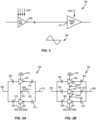
Figure 2 is a block diagram of an example transmission chain having a driving amplifier stage according to aspects of the present disclosure such that no inter-stage impedance network is required therebetween; -
Figure 3A is a circuit diagram of an example set of two stacked amplifiers to provide stacked transconductance devices that may be used to form the driving amplifier stage ofFigure 2 ; -
Figure 3B is a circuit diagram of an example set of three stacked amplifiers to provide stacked transconductance devices that may be used to form the driving amplifier stage ofFigure 2 ; -
Figure 4 is a circuit diagram of the two stacked amplifiers ofFigure 3A with additional detail about the supply voltage; -
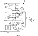
Figure 5 is a circuit diagram of the two stacked amplifiers ofFigure 3A with additional detail about possible biasing for the stacked transconductance devices; -
Figure 6 is a circuit diagram of two stacked amplifiers that provide a differential output to an output amplifier stage; -
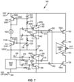
Figure 7 is a circuit diagram of the two stacked amplifiers ofFigure 5 with an expanded view of the output amplifier stage; -
Figure 8 is a circuit diagram of the three stacked amplifiers ofFigure 3B with additional detail about the biasing for the stacked transconductance devices; -
Figure 9 is a mixed block-circuit diagram showing a differential-to-single-ended arrangement of stacked transconductance devices according to the present disclosure; -
Figure 10 is a circuit diagram of the three stacked amplifiers ofFigure 3B with a possible supply source expanded; -
Figure 11 is a circuit diagram of a differential version of the three stacked amplifiers ofFigure 3B with an alternate possible supply source expanded; and -
Figure 12 is a circuit diagram of a quadrature version of the three stacked amplifiers ofFigure 3B with a power supply similar to that presented inFigure 11 . - The embodiments set forth below represent the necessary information to enable those skilled in the art to practice the embodiments and illustrate the best mode of practicing the embodiments. Upon reading the following description in light of the accompanying drawing figures, those skilled in the art will understand the concepts of the disclosure and will recognize applications of these concepts not particularly addressed herein. It should be understood that these concepts and applications fall within the scope of the disclosure and the accompanying claims.
- It will be understood that, although the terms first, second, etc. may be used herein to describe various elements, these elements should not be limited by these terms. These terms are only used to distinguish one element from another. For example, a first element could be termed a second element, and, similarly, a second element could be termed a first element, without departing from the scope of the present disclosure. As used herein, the term "and/or" includes any and all combinations of one or more of the associated listed items.
- It will be understood that when an element such as a layer, region, or substrate is referred to as being "on" or extending "onto" another element, it can be directly on or extend directly onto the other element or intervening elements may also be present. In contrast, when an element is referred to as being "directly on" or extending "directly onto" another element, there are no intervening elements present. Likewise, it will be understood that when an element such as a layer, region, or substrate is referred to as being "over" or extending "over" another element, it can be directly over or extend directly over the other element or intervening elements may also be present. In contrast, when an element is referred to as being "directly over" or extending "directly over" another element, there are no intervening elements present. It will also be understood that when an element is referred to as being "connected" or "coupled" to another element, it can be directly connected or coupled to the other element or intervening elements may be present. In contrast, when an element is referred to as being "directly connected" or "directly coupled" to another element, there are no intervening elements present.
- Relative terms such as "below" or "above" or "upper" or "lower" or "horizontal" or "vertical" may be used herein to describe a relationship of one element, layer, or region to another element, layer, or region as illustrated in the Figures. It will be understood that these terms and those discussed above are intended to encompass different orientations of the device in addition to the orientation depicted in the Figures.
- The terminology used herein is for the purpose of describing particular embodiments only and is not intended to be limiting of the disclosure. As used herein, the singular forms "a," "an," and "the" are intended to include the plural forms as well, unless the context clearly indicates otherwise. It will be further understood that the terms "comprises," "comprising," "includes," and/or "including" when used herein specify the presence of stated features, integers, steps, operations, elements, and/or components, but do not preclude the presence or addition of one or more other features, integers, steps, operations, elements, components, and/or groups thereof.
- Unless otherwise defined, all terms (including technical and scientific terms) used herein have the same meaning as commonly understood by one of ordinary skill in the art to which this disclosure belongs. It will be further understood that terms used herein should be interpreted as having a meaning that is consistent with their meaning in the context of this specification and the relevant art and will not be interpreted in an idealized or overly formal sense unless expressly so defined herein.
- Aspects disclosed in the detailed description include a driving amplifier stage with low output impedance. In particular, example aspects of the present disclosure contemplate a driving amplifier stage that does not need an inter-stage impedance matching network between the driving amplifier stage and an output amplifier stage in a transmission chain. The low output impedance of the driving amplifier stage may be achieved by providing stacking transconductance devices within the driving amplifier stage and reusing a supply current to provide an intermediate signal with high current but moderated voltage swing to drive the output amplifier stage. In specifically contemplated aspects, the stacked transconductance devices may be complementary metal oxide semiconductor (CMOS) field effect transistors (FETs). By providing a high current intermediate signal with moderate voltage swing, the need for an interstage matching circuit may be reduced or eliminated.
- Before addressing example aspects of the present disclosure a brief overview of a conventional power amplifier chain having a driving amplifier stage and an output amplifier stage with an inter-stage impedance circuit positioned therebetween is provided with reference to
Figure 1 to highlight the advantages of example aspects of the present disclosure. A discussion of example aspects begins below with reference toFigure 2 . - In this regard,
Figure 1 is a block diagram of atransmission chain 100 of a mobile computing device (not shown). A baseband signal containing information to be transmitted may be generated by a baseband processor (not shown) and converted to a frequency of interest (e.g., frequencies complying with the 5G-NR standard or other radio frequency (RF). This RF signal is provided to a driving amplifier stage 102. The driving amplifier stage 102 may be a FET, a bipolar junction transistor (BJT), or a heterojunction bipolar transistor (HBT). The driving amplifier stage 102 receives a low current (Low 1) from a voltage source (not shown) and outputs a largeswing voltage signal 104 atoutput 106 as a function of the relatively high impedance of the driving amplifier stage 102. Anoutput amplifier stage 108 is used to boost the signal to levels suitable for transmission and generally has alow impedance input 110, but takes a relatively high current (High 1) from a voltage source. Thelow impedance input 110 is configured to receive a relatively lowswing voltage signal 112. To transition the largeswing voltage signal 104 to the lowswing voltage signal 112, an inter-stage step-down impedance network orcircuit 114 is used to transform the signal as desired. - The presence of the inter-stage step-down
impedance circuit 114 imposes a physical cost in terms of space and bill of materials. For example, at the frequencies of interest, such a circuit is likely a higher order circuit with a relatively large inductor. Alternatively, such inter-stage step-downimpedance circuit 114 may impose severe bandwidth limitations, which are not desirable. Additionally, the presence of the inter-stage step-downimpedance circuit 114 may consume power and attenuate the signal to be transmitted by some amount, requiring extra amplification by theoutput amplifier stage 108. - Example aspects of the present disclosure provide an improved driving amplifier stage that allows the simplification or elimination of the inter-stage step-down
impedance circuit 114. Specifically, example aspects of the present disclosure provide a driving amplifier stage that has a reduced output impedance. The reduced output impedance is achieved by providing stacked transconductance devices. In specific aspects, the stacked transconductance devices use a stacked complementary amplifier configuration that provides a large stage gain by using a current reuse configuration. Elimination of the inter-stage step-downimpedance circuit 114 further allows for the signal path to the output amplifier stage to be wide bandwidth, which is important at the frequencies of interest. It should be appreciated that while elimination of the inter-stage step-downimpedance circuit 114 is desired, some alternating current (AC) coupling and/or optional high-pass filters may remain in place to assist in conditioning the signal for use by the output amplifier stage. - At its simplest, an example aspect of the present disclosure is illustrated by
transmission chain 200 inFigure 2 . As before, thetransmission chain 200 may include a baseband processor (not shown) and an intermediate frequency processor (also not shown) that generates an RF signal that is provided to a drivingamplifier stage 202. The drivingamplifier stage 202 receives a low current (Low I) from a voltage source (not shown) and outputs a lowswing voltage signal 204 atoutput 206. Anoutput amplifier stage 208 is used to boost the signal to levels suitable for transmission and generally has alow impedance input 210, but takes a relatively high current (High I) from a voltage source. Thelow impedance input 210 is configured to receive the relatively lowswing voltage signal 204. By generating the relatively lowswing voltage signal 204, there is reduced need for any inter-stage matching. In an example aspect, the inter-stage matching circuitry is eliminated. In an alternate example aspect, some AC coupling and optional high-pass filtering may be kept as some form of inter-stage network. However, such minimal circuitry should not hamper the signal path bandwidth. - The driving
amplifier stage 202 may be formed from stacked amplifiers that use an AC input split and output combining. Two examples of driving amplifier stages are provided inFigures 3A and 3B . Specifically,Figure 3A illustrates a drivingamplifier stage 300 having two stackedamplifiers stacked amplifiers input 306 throughcapacitors capacitors amplifier 302 may be coupled to a voltage source 318 (VDD) and may be an inverting or non-inverting amplifier. The twostacked amplifiers node 320, which may also be coupled to a voltage source 322 (mid-level voltage supply), which may be VDD/2 or the like as better explained below. Accordingly, thenode 320 may be referred to as a mid-level voltage supply input node which is configured to be held at a fraction of a voltage supply level to limit voltage swing across theamplifier 302. Theamplifier 304 may be coupled to thevoltage source 322 and to areference voltage 324, which may be VSS or a ground. -
Figure 3B illustrates a drivingamplifier stage 350 having three stackedamplifiers stacked amplifiers input 358 throughcapacitors capacitors amplifier 352 may be coupled to a voltage source 374 (VDD) and may be an inverting or non-inverting amplifier. Theamplifiers node 376, which may also be coupled to a voltage source 378 (Vsup1), which may be 2VDD/3, or the like as better explained below. Theamplifiers node 380, which may also be coupled to a voltage source 382 (Vsup2), which may be VDD/3 or the like as better explained below. Theamplifier 356 may be coupled to thevoltage source 382 and to areference voltage 384, which may be VSS or a ground. -
Figure 4 provides more details about the stacked amplifiers ofFigures 3A as well as one possible way that mid-level voltage supply may be provided. In particular, thepower amplifiers power amplifier 302 may include a p-type FET (PFET) 400 and an n-type FET (NFET) 402, and thepower amplifier 304 may include aPFET 404 and anNFET 406. Thecapacitor 308 may includeparallel capacitors capacitor 310 may includeparallel capacitors node 320, theoriginal voltage source 318 may be supplied to asupply voltage divider 418, which charges acapacitor 420 that may act as a filtering capacitance to provide an AC/RF supply current Iac to thenode 320. By holding thenode 320 at VDD/2 (i.e., half or a fraction of the voltage source 318), the rail-to-rail voltage swing of theamplifier amplifiers - The use of stacked FETs in this fashion provides a large transconductance gain. It should be appreciated that CMOS processes (e.g., silicon on insulator (SOI) CMOS processes) will use strained PFETs (e.g., Germanium (Ge) strained) so that the
PFETs NFETs comparable FETs FETs PFETs NFETs - The net result of the transconductance stacking of the
FETs output 312. It should be appreciated that a larger number of stacked CMOS stages can be placed on top of each other. Thus, for example, if the same stacking is applied to the drivingamplifier stage 350 ofFigure 3B , with Vsup1 being 2VDD/3 and Vsup2 being VDD/3, a nine-fold impedance reduction may be achieved. Accordingly, given a specific input impedance for anoutput amplifier stage 208, an appropriate stack size may be chosen to have a comparable impedance level, and thus avoid the need of a band limiting inter-stage step-downimpedance circuit 114. As an additional benefit for many CMOS processes, the battery supply is set for 3.4 volts (V), and thus, it may be possible to bias the drivingamplifier stage 350 directly from the battery since the FETs are designed for 1.2 V supply. That is, each of the paired stacks has a swing of one-third of the battery level, which is less than the designed 1.2 V. - While the above discussion has had a terse exploration of the circuits before the
power amplifiers power amplifiers Figure 5 provides additional details about example biasing circuitry. In particular, a signal arrives at theinput 306 and passes through thecapacitors FETs FETs gate 404G is also connected to abias circuit 500 through aresistor 502. Likewise, thegate 406G is also connected to thebias circuit 500 through aresistor 504. Thebias circuit 500 may be coupled to theground 324. - The
voltage supply 318 may be coupled to asource 400S. Additionally, thevoltage supply 318 may be coupled to asource 506S of aPFET 506. Agate 506G may be coupled to anode 508. Thenode 508 is coupled to thevoltage source 318 through acapacitor 510. Thenode 508 is coupled to agate 400G through aresistor 512. Adrain 506D may be coupled to adrain 514D of atransistor 514. Asource 514S may be coupled to thebias circuit 500. Agate 514G may be coupled to anode 516. Thenode 516 is coupled to agate 402G through aresistor 518. Thenode 516 may be coupled to thenode 320 through acapacitor 520. It should be appreciated that other bias circuits and bias networks may be used. - As illustrated, the
output amplifier stage 208 ofFigure 5 is single-ended and unipolar. The present disclosure is not so limited, and as illustrated inFigure 6 , a differential inputoutput amplifier stage 208D may be used with a drivingamplifier stage 600. The drivingamplifier stage 600 is substantially similar to the drivingamplifier stage 300 illustrated inFigure 5 . Twoadditional capacitors output amplifier stage 208D to thecommon drain nodes - By way of further illustration, the
output amplifier stage 208D may also be stacked transconductance devices as illustrated inFigure 7 . Specifically, theoutput amplifier stage 208D may includeFETs gates amplifier stage 300 previously described. TheFETs FETS FETs - While the above discussion has been primarily focused on the driving
amplifier stage 300,Figure 8 provides a similar expansion of the drivingamplifier stage 350 coupled to anoutput amplifier stage 800. Theoutput amplifier stage 800 may include stackedFETs FETs - The
amplifier 352 may be a stackedPFET 814 andNFET 816. Theamplifier 354 may be a stackedPFET 818 andNFET 820. Theamplifier 356 may be a stackedPFET 822 andNFET 824. In addition to thecapacitors capacitors amplifiers output amplifier stage 800. -
Bias circuits amplifiers Figure 5 . Again, the threestacked amplifiers -
Figure 9 provides an example of a completely differentialdriving amplifier stage 900 coupled to a differential-to-single-endedoutput amplifier stage 208D. The drivingamplifier stage 900 includes differential inputs 902(1), 902(2) and differential outputs 904(1), 904(2). The input 902(1) and output 904(1) are associated with stacked transconductance devices, namelyamplifiers amplifiers stacked transconductance devices amplifiers AC coupling capacitors - In the course of development, it was discovered that the capacitors used to support the mid voltage supplies (e.g.,
capacitor 420 ofFigure 4 ) are typically going to be fairly large. While a singlesuch capacitor 420 may be an acceptable design compromise for twostacked amplifiers amplifier stage 1000 inFigure 10 that has three stackedamplifiers large capacitors - Example aspects of the present disclosure provide an alternate solution to the
large capacitors Figures 11 and12 . Specifically, a mirrored arrangement is provided which allows for current to be reused between branches of the mirrored arrangement. - In this regard,
Figure 11 illustrates a differentialdriving amplifier stage 1100 with afirst stack 1102 and asecond stack 1104. Thefirst stack 1102 includes three stackedamplifiers second stack 1104 includes three stackedamplifiers Node 1118 exists betweenamplifiers node 1120 exists betweenamplifiers nodes node 1122 exists betweenamplifiers node 1124 exists betweenamplifiers node 1118 is coupled to thenode 1122, and thenode 1120 is coupled to thenode 1124. This arrangement allows current to be provided from thenode 1122 to thenode 1118 and vice versa depending on changes in the supply provided to thedifferent stacks node 1124 to thenode 1120 and vice versa. While there may be more devices in the drivingamplifier stage 1100 compared to the drivingamplifier stage 1000, the overall size may be reduced because of the elimination of thecapacitors - A similar advantage is provided in a quadrature structure as shown by the driving
amplifier stage 1200 illustrated inFigure 12 . The drivingamplifier stage 1200 includesstacks nodes nodes - The driving amplifier stage with low output impedance according to aspects disclosed herein may be provided in or integrated into any processor-based device. Examples, without limitation, include a set top box, an entertainment unit, a navigation device, a communications device, a fixed location data unit, a mobile location data unit, a global positioning system (GPS) device, a mobile phone, a cellular phone, a smart phone, a session initiation protocol (SIP) phone, a tablet, a phablet, a server, a computer, a portable computer, a mobile computing device, a wearable computing device (e.g., a smart watch, a health or fitness tracker, eyewear, etc.), a desktop computer, a personal digital assistant (PDA), a monitor, a computer monitor, a television, a tuner, a radio, a satellite radio, a music player, a digital music player, a portable music player, a digital video player, a video player, a digital video disc (DVD) player, a portable digital video player, an automobile, a vehicle component, avionics systems, a drone, and a multicopter.
- The previous description of the disclosure is provided to enable any person skilled in the art to make or use the disclosure. Various modifications to the disclosure will be readily apparent to those skilled in the art, and the generic principles defined herein may be applied to other variations. Thus, the disclosure is not intended to be limited to the examples and designs described herein, but is to be accorded the widest scope consistent with the principles and novel features disclosed herein.
- Further examples of feature combinations taught by the present disclosure are set out in the following numbered clauses:
- 1. A driving amplifier stage comprising:
- an input;
- an output; and
- an amplifier stack coupled to the input comprising:
- a first amplifier coupled to the input and the output;
- a second amplifier coupled to the input and coupled to the output such that a summed output signal is available at the output;
- a voltage supply input; and
- a mid-level voltage supply input node between the first amplifier and the second amplifier, wherein the mid-level voltage supply input node is configured to be held at a fraction of a voltage supply level to limit voltage swing across the first amplifier.
- 2. The driving amplifier stage of
clause 1, wherein the first amplifier comprises a first p-type field effect transistor (FET) (PFET) and a first n-type FET (NFET) stacked under the first PFET, wherein the first PFET is coupled to the voltage supply input and the first NFET is coupled to the mid-level voltage supply input node. - 3. The driving amplifier stage of
clause 2, wherein the second amplifier comprises a second PFET and a second NFET stacked under the second PFET, wherein the second PFET is coupled to the mid-level voltage supply input node. - 4. The driving amplifier stage of any preceding clause, wherein the mid-level voltage supply input node is coupled to a bypass capacitor.
- 5. The driving amplifier stage of any preceding clause, wherein the amplifier stack comprises a differential amplifier stack.
- 6. The driving amplifier stage of clause 5, wherein the mid-level voltage supply input node couples a first portion of the differential amplifier stack to a second portion of the differential amplifier stack.
- 7. The driving amplifier stage of any preceding clause, wherein the amplifier stack comprises a quadrature amplifier stack.
- 8. The driving amplifier stage of clause 7, wherein the mid-level voltage supply input node couples a first portion of the quadrature amplifier stack to a second portion, a third portion, and a fourth portion of the quadrature amplifier stack.
- 9. The driving amplifier stage of any preceding clause, further comprising a bias circuit coupled to the first amplifier.
- 10. The driving amplifier stage of any preceding clause, wherein the output comprises a differential output.
- 11. A driving amplifier stage comprising:
- an input configured to receive a radio frequency (RF) input; and
- an amplifier stack comprising:
- a first amplifier comprising a complementary metal oxide semiconductor (CMOS) arrangement of a first n-type field effect transistor (FET) (NFET) and a first p-type FET (PFET);
- a mid-level voltage supply input node coupled to the first amplifier;
- a second amplifier comprising a CMOS arrangement of a second NFET and a second PFET, the second PFET coupled to the mid-level voltage supply input node, wherein the first amplifier and the second amplifier share a current; and
- an output configured to provide a summed output signal from the first amplifier and the second amplifier.
- 12. The driving amplifier stage of clause 11, wherein the amplifier stack further comprises a third amplifier and a second mid-level voltage supply input node, wherein the second amplifier and the third amplifier are coupled to the second mid-level voltage supply input node.
- 13. The driving amplifier stage of clause 11 or clause 12, further comprising a capacitor positioned serially between the input and the first amplifier.
- 14. The driving amplifier stage of any of clauses 11 to 13, wherein the amplifier stack comprises a differential amplifier stack.
- 15. The driving amplifier stage of clause 14, wherein the mid-level voltage supply input node couples a first portion of the differential amplifier stack to a second portion of the differential amplifier stack.
- 16. The driving amplifier stage of any of clauses 11 to 15, wherein the amplifier stack comprises a quadrature amplifier stack.
- 17. The driving amplifier stage of clause 16, wherein the mid-level voltage supply input node couples a first portion of the quadrature amplifier stack to a second portion, a third portion, and a fourth portion of the quadrature amplifier stack.
- 18. An amplifier system comprising:
- a driving amplifier stage comprising:
- an input configured to receive a radio frequency (RF) input; and
- an amplifier stack comprising:
- a first amplifier comprising a complementary metal oxide semiconductor (CMOS) arrangement of a first n-type field effect transistor (FET) (NFET) and a first p-type FET (PFET);
- a mid-level voltage supply input node coupled to the first amplifier;
- a second amplifier comprising a CMOS arrangement of a second NFET and a second PFET, the second PFET coupled to the mid-level voltage supply input node, wherein the first amplifier and the second amplifier share a current; and
- an output configured to provide a summed output signal from the first amplifier and the second amplifier; and
- an output power amplifier stage coupled to the output.
- a driving amplifier stage comprising:
- 19. The amplifier system of clause 18, further comprising an interstage impedance transformation network positioned between the driving amplifier stage and the output power amplifier stage, wherein the interstage impedance transformation network is configured to provide no greater than a 2:1 impedance transformation.
- 20. The amplifier system of clause 18 or clause 19, wherein the output power amplifier stage is directly coupled to the driving amplifier stage.
Claims (15)
- A driving amplifier stage comprising:an input;an output; andan amplifier stack coupled to the input comprising:a first amplifier coupled to the input and the output;a second amplifier coupled to the input and coupled to the output such that a summed output signal is available at the output;a voltage supply input; anda mid-level voltage supply input node between the first amplifier and the second amplifier, wherein the mid-level voltage supply input node is configured to be held at a fraction of a voltage supply level to limit voltage swing across the first amplifier.
- The driving amplifier stage of claim 1, wherein the first amplifier comprises a first p-type field effect transistor (FET) (PFET) and a first n-type FET (NFET) stacked under the first PFET, wherein the first PFET is coupled to the voltage supply input and the first NFET is coupled to the mid-level voltage supply input node,
optionally wherein the second amplifier comprises a second PFET and a second NFET stacked under the second PFET, and wherein the second PFET is coupled to the mid-level voltage supply input node. - The driving amplifier stage of claim 1 or claim 2, wherein the mid-level voltage supply input node is coupled to a bypass capacitor.
- The driving amplifier stage of any preceding claim, wherein the amplifier stack comprises a differential amplifier stack, optionally, wherein the mid-level voltage supply input node couples a first portion of the differential amplifier stack to a second portion of the differential amplifier stack.
- The driving amplifier stage of any preceding claim, wherein the amplifier stack comprises a quadrature amplifier stack, optionally wherein the mid-level voltage supply input node couples a first portion of the quadrature amplifier stack to a second portion, a third portion, and a fourth portion of the quadrature amplifier stack.
- The driving amplifier stage of any preceding claim, further comprising a bias circuit coupled to the first amplifier.
- The driving amplifier stage of any preceding claim, wherein the output comprises a differential output.
- A driving amplifier stage comprising:an input configured to receive a radio frequency (RF) input; andan amplifier stack comprising:a first amplifier comprising a complementary metal oxide semiconductor (CMOS) arrangement of a first n-type field effect transistor (FET) (NFET) and a first p-type FET (PFET);a mid-level voltage supply input node coupled to the first amplifier;a second amplifier comprising a CMOS arrangement of a second NFET and a second PFET, the second PFET coupled to the mid-level voltage supply input node, wherein the first amplifier and the second amplifier share a current; andan output configured to provide a summed output signal from the first amplifier and the second amplifier.
- The driving amplifier stage of claim 8, wherein the amplifier stack further comprises a third amplifier and a second mid-level voltage supply input node, wherein the second amplifier and the third amplifier are coupled to the second mid-level voltage supply input node.
- The driving amplifier stage of claim 8 or claim 9, further comprising a capacitor positioned serially between the input and the first amplifier.
- The driving amplifier stage of any of claims 8 to 10, wherein the amplifier stack comprises a differential amplifier stack, optionally wherein the mid-level voltage supply input node couples a first portion of the differential amplifier stack to a second portion of the differential amplifier stack.
- The driving amplifier stage of any of claims 8 to 11, wherein the amplifier stack comprises a quadrature amplifier stack, optionally wherein the mid-level voltage supply input node couples a first portion of the quadrature amplifier stack to a second portion, a third portion, and a fourth portion of the quadrature amplifier stack.
- An amplifier system comprising:a driving amplifier stage comprising:an input configured to receive a radio frequency (RF) input; andan amplifier stack comprising:a first amplifier comprising a complementary metal oxide semiconductor (CMOS) arrangement of a first n-type field effect transistor (FET) (NFET) and a first p-type FET (PFET);a mid-level voltage supply input node coupled to the first amplifier;a second amplifier comprising a CMOS arrangement of a second NFET and a second PFET, the second PFET coupled to the mid-level voltage supply input node, wherein the first amplifier and the second amplifier share a current; andan output configured to provide a summed output signal from the first amplifier and the second amplifier; andan output power amplifier stage coupled to the output.
- The amplifier system of claim 13, further comprising an interstage impedance transformation network positioned between the driving amplifier stage and the output power amplifier stage, wherein the interstage impedance transformation network is configured to provide no greater than a 2:1 impedance transformation.
- The amplifier system of claim 13 or claim 14, wherein the output power amplifier stage is directly coupled to the driving amplifier stage.
Applications Claiming Priority (1)
| Application Number | Priority Date | Filing Date | Title |
|---|---|---|---|
| US17/588,867 US12160210B2 (en) | 2022-01-31 | 2022-01-31 | Driving amplifier stage with low output impedance |
Publications (1)
| Publication Number | Publication Date |
|---|---|
| EP4220953A1 true EP4220953A1 (en) | 2023-08-02 |
Family
ID=85150166
Family Applications (1)
| Application Number | Title | Priority Date | Filing Date |
|---|---|---|---|
| EP23153991.7A Pending EP4220953A1 (en) | 2022-01-31 | 2023-01-30 | Driving amplifier stage with low output impedance |
Country Status (3)
| Country | Link |
|---|---|
| US (1) | US12160210B2 (en) |
| EP (1) | EP4220953A1 (en) |
| CN (1) | CN116526994A (en) |
Families Citing this family (2)
| Publication number | Priority date | Publication date | Assignee | Title |
|---|---|---|---|---|
| US11936346B2 (en) * | 2021-04-15 | 2024-03-19 | Texas Instruments Incorporated | Programmable gain low noise amplifier |
| CN121791835B (en) * | 2026-03-03 | 2026-05-05 | 成都铭科思微电子技术有限责任公司 | A CMOS ultrawideband high-gain high-power amplifier |
Citations (3)
| Publication number | Priority date | Publication date | Assignee | Title |
|---|---|---|---|---|
| US6285251B1 (en) * | 1998-04-02 | 2001-09-04 | Ericsson Inc. | Amplification systems and methods using fixed and modulated power supply voltages and buck-boost control |
| US20110109393A1 (en) * | 2009-11-12 | 2011-05-12 | Jaroslaw Edward Adamski | Stacked pre-driver amplifier |
| WO2020006990A1 (en) * | 2018-07-06 | 2020-01-09 | Shenzhen GOODIX Technology Co., Ltd. | Stacked power amplifiers using core devices |
Family Cites Families (6)
| Publication number | Priority date | Publication date | Assignee | Title |
|---|---|---|---|---|
| US5200708A (en) * | 1991-09-11 | 1993-04-06 | Thomson Consumer Electronics, Inc. | Apparatus for the virtual expansion of power supply capacity |
| US6825719B1 (en) * | 2000-05-26 | 2004-11-30 | Intel Corporation | RF power amplifier and methods for improving the efficiency thereof |
| US8130043B2 (en) * | 2003-09-25 | 2012-03-06 | Anadigics, Inc. | Multi-stage power amplifier with enhanced efficiency |
| JP5338262B2 (en) * | 2008-11-05 | 2013-11-13 | 日本電気株式会社 | Power amplifier and amplification method thereof |
| US9166536B2 (en) * | 2012-10-30 | 2015-10-20 | Eta Devices, Inc. | Transmitter architecture and related methods |
| US8824978B2 (en) * | 2012-10-30 | 2014-09-02 | Eta Devices, Inc. | RF amplifier architecture and related techniques |
-
2022
- 2022-01-31 US US17/588,867 patent/US12160210B2/en active Active
-
2023
- 2023-01-30 CN CN202310044801.7A patent/CN116526994A/en active Pending
- 2023-01-30 EP EP23153991.7A patent/EP4220953A1/en active Pending
Patent Citations (3)
| Publication number | Priority date | Publication date | Assignee | Title |
|---|---|---|---|---|
| US6285251B1 (en) * | 1998-04-02 | 2001-09-04 | Ericsson Inc. | Amplification systems and methods using fixed and modulated power supply voltages and buck-boost control |
| US20110109393A1 (en) * | 2009-11-12 | 2011-05-12 | Jaroslaw Edward Adamski | Stacked pre-driver amplifier |
| WO2020006990A1 (en) * | 2018-07-06 | 2020-01-09 | Shenzhen GOODIX Technology Co., Ltd. | Stacked power amplifiers using core devices |
Non-Patent Citations (1)
| Title |
|---|
| MONDAL SOMOK ET AL: "An ECG chopper amplifier achieving 0.92 NEF and 0.85 PEF with AC-coupled inverter-stacking for noise efficiency enhancement", 2017 IEEE INTERNATIONAL SYMPOSIUM ON CIRCUITS AND SYSTEMS (ISCAS), IEEE, 28 May 2017 (2017-05-28), pages 1 - 4, XP033156565, DOI: 10.1109/ISCAS.2017.8050957 * |
Also Published As
| Publication number | Publication date |
|---|---|
| US20230246611A1 (en) | 2023-08-03 |
| CN116526994A (en) | 2023-08-01 |
| US12160210B2 (en) | 2024-12-03 |
Similar Documents
| Publication | Publication Date | Title |
|---|---|---|
| JP4713939B2 (en) | Voltage controlled oscillator and wireless communication device using the same | |
| US12081243B2 (en) | Low noise amplifiers with combined outputs | |
| US7432763B2 (en) | Gain boosting for tuned differential LC circuits | |
| US8483627B2 (en) | Circuits, processes, devices and systems for full integration of RF front end module including RF power amplifier | |
| US7705682B2 (en) | Inductor sharing in radio frequency communications | |
| US9484888B2 (en) | Linear resistor with high resolution and bandwidth | |
| US8552788B2 (en) | Apparatus and methods for adaptive common-mode level shifting | |
| US12160210B2 (en) | Driving amplifier stage with low output impedance | |
| US7961050B1 (en) | Integrated circuits including an equalizer and operating methods thereof | |
| JP2001036381A (en) | Mutual conductance amplifier, transmitter including the amplifier and integrated circuit | |
| US8324966B2 (en) | Apparatus and methods for electronic amplification | |
| US12191816B2 (en) | Complementary balanced low-noise amplifier circuit | |
| US7176759B2 (en) | Differential low noise amplifier with low power consumption | |
| JP2006521729A (en) | Random sequence generator | |
| TW202441900A (en) | Kickback reduction in bootstrapped switches | |
| US20140266439A1 (en) | Methods and systems to provide low noise amplification | |
| EP4437651B1 (en) | Power amplifier having improved gate oxide integrity | |
| JP2002314355A (en) | Multistage amplifier circuit | |
| JP4140296B2 (en) | Amplifier circuit | |
| WO2017046447A1 (en) | Method and apparatus for amplifying signals | |
| WO2025207200A1 (en) | Current reuse low noise amplifier (lna) | |
| HK40107545A (en) | Power amplifier having improved gate oxide integrity | |
| WO2025188440A1 (en) | Active balun | |
| EP3139498A1 (en) | Method and apparatus for amplifying signals | |
| JP2006254158A (en) | Variable gain amplifier |
Legal Events
| Date | Code | Title | Description |
|---|---|---|---|
| PUAI | Public reference made under article 153(3) epc to a published international application that has entered the european phase |
Free format text: ORIGINAL CODE: 0009012 |
|
| STAA | Information on the status of an ep patent application or granted ep patent |
Free format text: STATUS: THE APPLICATION HAS BEEN PUBLISHED |
|
| AK | Designated contracting states |
Kind code of ref document: A1 Designated state(s): AL AT BE BG CH CY CZ DE DK EE ES FI FR GB GR HR HU IE IS IT LI LT LU LV MC ME MK MT NL NO PL PT RO RS SE SI SK SM TR |
|
| STAA | Information on the status of an ep patent application or granted ep patent |
Free format text: STATUS: REQUEST FOR EXAMINATION WAS MADE |
|
| 17P | Request for examination filed |
Effective date: 20240129 |
|
| RBV | Designated contracting states (corrected) |
Designated state(s): AL AT BE BG CH CY CZ DE DK EE ES FI FR GB GR HR HU IE IS IT LI LT LU LV MC ME MK MT NL NO PL PT RO RS SE SI SK SM TR |