EP4220855A1 - Patch antenna - Google Patents
Patch antenna Download PDFInfo
- Publication number
- EP4220855A1 EP4220855A1 EP21872615.6A EP21872615A EP4220855A1 EP 4220855 A1 EP4220855 A1 EP 4220855A1 EP 21872615 A EP21872615 A EP 21872615A EP 4220855 A1 EP4220855 A1 EP 4220855A1
- Authority
- EP
- European Patent Office
- Prior art keywords
- radiating element
- cable
- parasitic element
- patch antenna
- parasitic
- Prior art date
- Legal status (The legal status is an assumption and is not a legal conclusion. Google has not performed a legal analysis and makes no representation as to the accuracy of the status listed.)
- Pending
Links
- 230000003071 parasitic effect Effects 0.000 claims abstract description 99
- 239000000758 substrate Substances 0.000 claims description 18
- 230000004308 accommodation Effects 0.000 claims description 2
- 230000005855 radiation Effects 0.000 description 19
- 230000000052 comparative effect Effects 0.000 description 10
- 238000010586 diagram Methods 0.000 description 9
- 238000004088 simulation Methods 0.000 description 6
- 239000004020 conductor Substances 0.000 description 5
- 238000000034 method Methods 0.000 description 5
- 238000012986 modification Methods 0.000 description 5
- 230000004048 modification Effects 0.000 description 5
- 230000002159 abnormal effect Effects 0.000 description 2
- 230000000694 effects Effects 0.000 description 2
- 239000000853 adhesive Substances 0.000 description 1
- 230000001070 adhesive effect Effects 0.000 description 1
- 230000002411 adverse Effects 0.000 description 1
- 239000000919 ceramic Substances 0.000 description 1
- 238000004891 communication Methods 0.000 description 1
- 230000008878 coupling Effects 0.000 description 1
- 238000010168 coupling process Methods 0.000 description 1
- 238000005859 coupling reaction Methods 0.000 description 1
- 238000004519 manufacturing process Methods 0.000 description 1
- 230000000149 penetrating effect Effects 0.000 description 1
- 239000011347 resin Substances 0.000 description 1
- 229920005989 resin Polymers 0.000 description 1
- 229910000679 solder Inorganic materials 0.000 description 1
Images







Classifications
-
- H—ELECTRICITY
- H01—ELECTRIC ELEMENTS
- H01Q—ANTENNAS, i.e. RADIO AERIALS
- H01Q9/00—Electrically-short antennas having dimensions not more than twice the operating wavelength and consisting of conductive active radiating elements
- H01Q9/04—Resonant antennas
- H01Q9/0407—Substantially flat resonant element parallel to ground plane, e.g. patch antenna
-
- H—ELECTRICITY
- H01—ELECTRIC ELEMENTS
- H01Q—ANTENNAS, i.e. RADIO AERIALS
- H01Q5/00—Arrangements for simultaneous operation of antennas on two or more different wavebands, e.g. dual-band or multi-band arrangements
- H01Q5/30—Arrangements for providing operation on different wavebands
- H01Q5/378—Combination of fed elements with parasitic elements
-
- H—ELECTRICITY
- H01—ELECTRIC ELEMENTS
- H01Q—ANTENNAS, i.e. RADIO AERIALS
- H01Q1/00—Details of, or arrangements associated with, antennas
- H01Q1/12—Supports; Mounting means
- H01Q1/1271—Supports; Mounting means for mounting on windscreens
-
- H—ELECTRICITY
- H01—ELECTRIC ELEMENTS
- H01Q—ANTENNAS, i.e. RADIO AERIALS
- H01Q15/00—Devices for reflection, refraction, diffraction or polarisation of waves radiated from an antenna, e.g. quasi-optical devices
-
- H—ELECTRICITY
- H01—ELECTRIC ELEMENTS
- H01Q—ANTENNAS, i.e. RADIO AERIALS
- H01Q19/00—Combinations of primary active antenna elements and units with secondary devices, e.g. with quasi-optical devices, for giving the antenna a desired directional characteristic
- H01Q19/005—Patch antenna using one or more coplanar parasitic elements
Definitions
- the present invention relates to a patch antenna.
- V2X vehicle-to-everything
- a technique of a patch antenna in which long linear parasitic elements are disposed along sides in the outside of two opposing sides of a radiating element see, for example, Patent Literature 1 and Patent Literature 2.
- a method of routing a power supply cable on a back surface side of the patch antenna is considered.
- a method of routing a power supply cable on a back surface side of the patch antenna is considered.
- the cable of the antenna attached to the windshield or the rear window in the inside of a vehicle body interior if the cable extends from the back surface side of the antenna, it is difficult to route the cable.
- the cable routing may affect antenna characteristics.
- An example of an object of the present invention is to implement cable routing that has a small influence on antenna characteristics in a patch antenna having a parasitic element.
- An aspect of the present invention is a patch antenna including a planar radiating element, a parasitic element provided at a position spaced apart from the radiating element in a plan view when the radiating element is viewed from a direction perpendicular to a surface of the radiating element, and a cable electrically connected to the radiating element and configured to supply power to the radiating element, in which when a direction along the cable passing through a position where the cable is electrically connected to the radiating element is defined as a cable connection direction, a virtual line in the cable connection direction is positioned away from a center of the parasitic element.
- an aspect of the present invention is a patch antenna including a planar radiating element, a parasitic element provided at a position spaced apart from an end portion of the radiating element in a plan view when the radiating element is viewed from a direction perpendicular to a surface of the radiating element, and a cable electrically connected to the radiating element and configured to supply power to the radiating element, in which an axis of the cable passing through a position where the cable is electrically connected to the radiating element is spaced apart from a center of the parasitic element.
- the X-axis positive direction is referred to as the front
- an X-axis negative direction is referred to as the rear
- a Z-axis positive direction is referred to as the upper
- a Z-axis negative direction is referred to as the lower
- a Y-axis positive direction is referred to as the left
- a Y-axis negative direction is referred to as the right as appropriate.
- Fig. 1 is a diagram showing an attachment state of an antenna device 10 for a vehicle (an antenna device 10) of the present embodiment, and the upper part is an enlarged view of the attachment state of the antenna device 10.
- Fig. 2 is a perspective external view of the antenna device 10 as viewed obliquely from a front left upper side.
- Fig. 3 is a perspective external view of the antenna device 10 as viewed obliquely from the rear right upper side.
- Fig. 4 is an exploded view of the antenna device 10.
- the antenna device 10 includes a bracket 11 and a patch antenna 20.
- the bracket 11 is attached to a windshield 6 of the vehicle 5.
- the patch antenna 20 is fixed to the bracket 11 in a posture in which a front surface faces a front side of the vehicle 5.
- the antenna device 10 may be attached to a rear window of the vehicle 5.
- the bracket 11 includes an inclined surface 12 and a holding portion 13.
- the inclined surface 12 is a surface to be attached to the windshield 6.
- the holding portion 13 holds the patch antenna 20.
- a plurality of types of brackets 11 having different angles of the inclined surface 12 are prepared in advance.
- the bracket 11 of a type suitable for an inclination angle of the windshield 6 of the vehicle 5 to which the antenna device 10 is attached is selected and used.
- the holding portion 13 is a saucer-shaped portion extending downward from an upper end portion of the inclined surface 12.
- the patch antenna 20 is inserted into and fixed to the holding portion 13 from above.
- Fig. 5 is an exploded view of the patch antenna 20.
- the patch antenna 20 includes, in an internal space, an antenna body 30, a substrate (PCB: printed-circuit board) 40, and a routing structure 50 for a power supply cable.
- the internal space is defined by bringing a case 21 and a base 22 into contact with each other and coupling and fixing the case 21 and the base 22 with screws 23.
- the antenna body 30 is fixed to the case 21 and the base 22 by fastening the substrate 40 to the case 21 and the base 22 with the screws 23. As a result, for example, it is possible to prevent abnormal noises caused by vibration or the like during traveling.
- a cable 52 is connected to a connection terminal 51 provided on the substrate 40.
- a "prying force" may be generated via the cable 52 when the antenna device 10 is installed in the vehicle 5.
- the "prying force" is transmitted to the case 21 and the base 22 via the connection terminal 51 and the screws 23. Therefore, it is possible to prevent the "prying force" from acting on the antenna body 30 and to prevent the influence of the "prying force" on a circuit of the antenna body 30 and a joint portion of solder or the like.
- the antenna body 30 includes a planar radiating element 32, a pair of parasitic elements 33, and a ground conductor 34.
- the radiating element 32 is disposed on a surface side (a front surface side: an X-axis positive direction side) of a dielectric 31.
- the ground conductor 34 is positioned on a back surface side (a rear surface side: an X-axis negative direction side) of the dielectric 31.
- the dielectric 31 is a dielectric substrate, but the dielectric 31 may be a member made of ceramic or a member made of resin.
- the radiating element 32 is electrically connected to a pin 24 penetrating the dielectric 31 and the ground conductor 34 at a feeding point 39, and is electrically connected to the routing structure 50 for a power supply cable via the substrate 40 to which an end portion of the pin 24 is connected.
- the parasitic element 33 is a linear conductor having a rectangular (quadrilateral) shape in a plan view when the radiating element 32 is viewed from an X-axis positive direction side in a direction (the normal direction) perpendicular to a surface of the radiating element 32.
- the parasitic element 33 is provided at a position spaced apart from the radiating element 32 in a plan view. It can also be said that the parasitic element 33 is provided at a position spaced apart from an end portion of the radiating element 32 in a plan view.
- one parasitic element 33 is provided on each of a Y-axis positive side and a Y-axis negative side with a longitudinal direction of the parasitic element 33 as a direction along a line connecting a center P4 of the radiating element 32 (a geometric center of the radiating element 32) and the feeding point 39 of the radiating element 32 in a plan view.
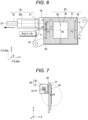
- Fig. 6 is a front view of the patch antenna 20 showing a relative positional relation between the antenna body 30 and the routing structure 50.
- Fig. 7 is a side view of the patch antenna 20 showing the relative positional relation between the antenna body 30 and the routing structure 50.
- the routing structure 50 is a structure in which the cable 52 that is electrically connected to the radiating element 32 and supplies power to the radiating element 32 is routed from the side of the antenna body 30 where the parasitic element 33 is positioned.
- the routing structure 50 includes the connection terminal 51 that is a connection destination of a connection terminal 52a provided at a distal end of the cable 52 such as a coaxial cable.
- the cable 52 is electrically connected to the radiating element 32 via the connection terminal 51 connected to the substrate 40.
- Fig. 6 shows a state in which the cable 52 is connected.
- the routing structure 50 may further include, in addition to the connection terminal 51, the connection terminal 52a on the cable 52 side connected to the connection terminal 51 and the cable 52.
- the routing structure 50 may include the cable 52.
- the configuration in which the cable 52 is connected via the connection terminal 51 or the connection terminal 52a facilitates an attachment operation.
- a shape of the connection terminal 51 may be an I-shape or an L-shape. Even if a standard of the cable 52 is different depending on a type of the vehicle 5, a specification can be changed flexibly and easily by changing a type of the connection terminal 51.
- a configuration in which the cable 52 is directly connected to a back surface (a surface on the X-axis negative direction side) of the substrate 40 may be adopted, and the connection terminal 51 may be omitted.
- a direction indicated by an arrow indicates a cable connection direction.
- the cable connection direction is an extension direction of the cable 52 extending from the connection terminal 51, in other words, a direction along the cable 52 passing through a position where the cable 52 is electrically connected to the radiating element 32.
- a reference numeral D1 shown in Figs. 6 and 7 denotes a virtual line in the cable connection direction. In the present embodiment, for easier understanding, the virtual line D1 is represented as an axis of the cable 52 extending from the connection terminal 51.
- a central axis portion that linearly extends from a position where the cable 52 is electrically connected to the radiating element 32 is represented as the axis of the cable 52.
- the central axis portion that linearly extends from the position where the cable 52 is electrically connected to the radiating element 32 is represented as the axis of the cable 52.
- a point where the virtual line (the axis of the cable 52) D1 in the cable connection direction and a spherical surface of a virtual sphere centered on a center (a geometric center of the parasitic element 33) P3 of the parasitic element 33 are in contact with each other is defined as a position P1.
- the position P1 is a position where a distance between the virtual line D1 and the center P3 of the parasitic element 33 is the shortest. Therefore, a distance W between the position P1 and the center P3 of the parasitic element 33 is also the distance W between the virtual line D1 and the center P3 of the parasitic element 33.
- the position P1 is shown as if it is on the parasitic element 33, but actually, as shown in Fig. 7 , the position P1 is on the X-axis negative direction from the parasitic element 33.
- the routing structure 50 is a structure in which the virtual line D1 is positioned away from the center P3 of the parasitic element 33. Specifically, in a plan view in which the radiating element 32 is viewed from an X-axis positive side in the direction perpendicular to the surface of the radiating element 32, (1) the virtual line D1 does not pass through the center P3 (a small black circle in Fig. 6 ) of the parasitic element 33 (that is, the virtual line D1 is positioned away from the center P3 of the parasitic element 33), and (2) the virtual line D1 is substantially parallel to the surface of the radiating element 32.
- the cable connection direction is set to (3) a direction intersecting the longitudinal direction of the parasitic element 33.
- the virtual line D1 is disposed on a side where the feeding point 39 of the radiating element 32 is disposed with respect to the center P3 of the parasitic element 33.
- the parasitic element 33 is disposed between the connection terminal 51 of the routing structure 50 and the radiating element 32 in the plan view.
- the distance W between the virtual line D1 and the center P3 of the parasitic element 33 is set to be approximately ⁇ /26 or more, more preferably approximately ⁇ /13 or more, where ⁇ is a frequency for use.
- routing structure 50 it is possible to implement cable routing that has a small influence on antenna characteristics.
- a simulation result regarding the patch antenna 20 having the routing structure 50 will be described.
- Fig. 8A shows a relative positional relation between the antenna body 30 and the routing structure 50.
- Fig. 8B shows a radiation pattern in which a radiation directivity of an H plane (an XY plane) related to the patch antenna 20 in Fig. 8A when a length L of the parasitic element 33 is changed is shown by polar coordinates.
- the used frequency ⁇ is 5,900 MHz, and the distance W is 6 mm.
- Fig. 9A shows a relative positional relation between the antenna body 30 and the routing structure 50 of a comparative example created by changing the distance W of the patch antenna 20.
- FIG. 9B shows a radiation pattern in which a radiation directivity of the H plane according to the patch antenna of the comparative example is shown by polar coordinates when the length L of the parasitic element 33 is changed.
- the position P1 is a position where the connection terminal 51 and the like do not interfere with the parasitic element 33, and is a position where a distance from the center P3 of the parasitic element 33 is minimized.
- the used frequency ⁇ is 5,900 MHz.
- a line type indicates a difference in the length L of the parasitic element 33.
- the 3 dB beam width is in a range of 87.3 degrees to 89.5 degrees. Even if the length L of the parasitic element 33 is changed, a difference between a maximum value and a minimum value of the 3 dB beam width is 2.2 degrees.
- the directivity can be further widened by further increasing the length L of the parasitic element 33.
- the directivity can be narrowed by further reducing the length L of the parasitic element 33.
- the influence of the cable routing on the antenna characteristics can be reduced, and the directivity can be adjusted by the length L of the parasitic element 33.
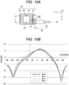
- Fig. 10A shows a relative positional relation between the antenna body 30 and the routing structure 50.
- Fig. 10B shows a radiation pattern in which a radiation directivity on the H plane is shown in orthogonal coordinates when the length L of the parasitic element 33 is fixed, the virtual line D1 is shifted to a Z-axis positive side (a side closer to the feeding point 39), and the distance W in the relative positional relation of Fig. 10A is changed.
- Fig. 11A shows a relative positional relation between the antenna body 30 and the routing structure 50.
- Fig. 11B shows a radiation pattern in which a radiation directivity on the H plane is shown in orthogonal coordinates when the length L of the parasitic element 33 is fixed, the virtual line D1 is shifted to a Z-axis negative side (a side away from the feeding point 39), and the distance W in the relative positional relation of Fig. 11A is changed.
- a solid line indicates a case where the parasitic element 33 is "present”
- a broken line indicates a case where the parasitic element 33 is "absent”.
- the distance W is approximately 1.8 mm or more, which is approximately ⁇ /26 or more.
- ⁇ of minus 45 degrees it is more preferable to set a distance W at which a gain increase of about 1 dB or more is obtained compared to when the distance W is set to 0 (zero). Therefore, according to Fig. 12 , it is more preferable that the distance W is approximately 3.7 mm or more, which is approximately ⁇ /13 or more, at which a gain increase larger than 1 dB can be expected.
- Figs. 13 and 14 are diagrams showing a simulation result of an intensity distribution of a surface current in a steady state.
- Fig. 13 is a simulation result of the patch antenna 20 of the present embodiment when the virtual line D1 is separated by a distance W of 6 mm to the feeding point 39 side.
- Fig. 14 is a simulation result of a patch antenna in which the distance W is set to 0 (zero) as a comparative example.
- the intensity of a surface current of the parasitic element 33 on a side closer to the connection terminal 51 and an around the parasitic element 33 is shown by an ellipse of a broken line in Figs. 13 and 14 .
- the center P3 of the parasitic element 33 is shown by a white arrow.
- the patch antenna 20 of the above embodiment may be a two-point feeding type patch antenna such as a circularly polarized patch antenna.
- an antenna body 30B includes parasitic elements 33 and parasitic elements 35 in the outside of four sides of the radiating element 32.
- the parasitic elements 33 are disposed on a Y-axis positive direction side and a Y-axis negative direction side with respect to the radiating element 32 to form a pair.
- the parasitic elements 35 are disposed on a Z-axis positive direction side and a negative direction side with respect to the radiating element 32 to form a pair.
- the radiating element 32 includes the first feeding point 39 and a second feeding point 36.
- the virtual line D1 is set along a Y-axis. Therefore, a distance W3 is determined in the same manner as the distance W of the above embodiment with reference to the parasitic element 33 on the Y-axis positive direction side close to the routing structure 50 out of the parasitic elements 33. In this case, a high gain can be obtained by separating the virtual line D1 to the sides where the feeding point 36 and the feeding point 39 are positioned, rather than separating the virtual line D1 to a side where the feeding point 36 or the feeding point 39 is not positioned.
- the virtual line D1 does not necessarily have to be orthogonal to a virtual line D3 in a longitudinal direction of the parasitic element 33 in a plan view.
- the virtual line D1 may be in a direction intersecting the virtual line D3, for example, may be set to be inclined with respect to the virtual line D3.
- the virtual line D3 represents a line (an axis) that passes through the center (the geometric center) P3 of the parasitic element 33 and connects short sides of the parasitic element 33.
- the virtual line D3 represents a line that passes through the center (the geometric center) P3 of the parasitic element 33 and is parallel to long sides of the parasitic element 33.
- an antenna device 10C for a vehicle shown in Fig. 16 includes a patch antenna 20C, a bracket 11C to be attached to the windshield 6, and a cover 18.
- the patch antenna 20C includes a case 21C that accommodates an antenna body, the cable 52, and a connector 56 provided at a distal end of the cable 52.
- the case 21C is held by a distal end holding portion 15 of the bracket 11C, and the connector 56 is held by a rear end holding portion 16 of the bracket 11C.
- the cover 18 accommodates the antenna device 10C to cover a surface other than a bonding surface to the windshield 6.
- the patch antenna 20C basically has the same configuration as the antenna body 30 of the above embodiment, but a routing structure 50C is different from the routing structure 50 of the antenna body 30.
- the routing structure 50C includes, instead of the connection terminal 51, the cable 52 having one end fixed to the substrate 40, and the connector 56 provided at the distal end of the cable 52. A fixing position of the cable 52 and the substrate 40 satisfies the same conditions as the conditions related to the routing structure 50 in the antenna body 30.
- the virtual line D1 in the routing structure 50C is set to form an angle of 45° with respect to the virtual line D3 in the longitudinal direction of the parasitic element 33 shown in Fig. 6 in a plan view viewed from an X-axis positive direction.
- An example of a method of attaching the antenna device 10C is as follows. First, the bracket 11C is attached to the windshield 6. Next, the patch antenna 20C is inserted into and fixed to the distal end holding portion 15 of the bracket 11C from the side, and the connector 56 is pressed into and fixed to the rear end holding portion 16 from the side. Finally, the cover 18 is attached to the bracket 11C along an XZ plane to slide obliquely from a front lower side to a rear upper side along the windshield 6.
- a width in a Y-axis direction required for routing the cable 52 can be reduced.
- a degree of freedom of an attachment position of the antenna device 10C increases accordingly.
- Setting the virtual line D1 obliquely with respect to the virtual line D3 means that an angle formed by the virtual line D1 and the virtual line D3 is an angle other than 90 degrees and 180 degrees, and includes, for example, approximately 45 degrees in a YZ plane and approximately 45 degrees in the XZ plane.
- the opportunity to apply a load for pushing up the windshield 6 from a vehicle interior side can be limited to the time of attaching the bracket 11C.
- an adhesive on the windshield 6 attached to the vehicle 5 may not be sufficiently cured.
- the antenna device 10C can be attached without applying a load that excessively pushes up the windshield 6 according to the attachment method described above.
- An aspect of the present disclosure is a patch antenna including a planar radiating element, a parasitic element provided at a position spaced apart from the radiating element in a plan view when the radiating element is viewed from a direction perpendicular to a surface of the radiating element, and a cable electrically connected to the radiating element and configured to supply power to the radiating element, in which when a direction along the cable passing through a position where the cable is electrically connected to the radiating element is defined as a cable connection direction, a virtual line in the cable connection direction is positioned away from a center of the parasitic element.
- an aspect of the present disclosure is a patch antenna including a planar radiating element, a parasitic element provided at a position spaced apart from an end portion of the radiating element in a plan view when the radiating element is viewed from a direction perpendicular to a surface of the radiating element, and a cable electrically connected to the radiating element and configured to supply power to the radiating element, in which an axis of the cable passing through a position where the cable is electrically connected to the radiating element is spaced apart from a center of the parasitic element.
- a distance between the virtual line (the axis) and the center of the parasitic element may be approximately ⁇ /26 or more, where ⁇ is a frequency for use.
- a distance between the virtual line (the axis) and the center of the parasitic element may be approximately ⁇ /13 or more, where ⁇ is a frequency for use.
- the parasitic element may have a rectangular shape in the plan view, and the cable connection direction may be a direction intersecting a longitudinal direction of the parasitic element in the plan view.
- the parasitic element may have a rectangular shape in the plan view, and the axis may intersect a line parallel to the longitudinal direction of the parasitic element in the plan view.
- the longitudinal direction of the parasitic element may be a direction along a line connecting a center of the radiating element and a feeding point of the radiating element in the plan view, and the virtual line (the axis) may be disposed on a side where the feeding point of the radiating element is positioned with respect to the center of the parasitic element in the plan view.
- the patch antenna may further include a connection terminal that connects the cable to the radiating element.
- the parasitic element may be disposed between the connection terminal and the radiating element in the plan view.
- the patch antenna may include the cable and a connector connected to a distal end of the cable.
- the patch antenna may further include a substrate on which the radiating element and the parasitic element are provided and to which the radiating element and the cable are electrically connected, a base on which the substrate is disposed, and a case forming an accommodation space for accommodating the base, the radiating element, the parasitic element, and in which the substrate, and the case, the substrate, and the base are fastened together.
Landscapes
- Waveguide Aerials (AREA)
- Details Of Aerials (AREA)
- Support Of Aerials (AREA)
- Aerials With Secondary Devices (AREA)
Abstract
Description
- The present invention relates to a patch antenna.
- As a vehicle-to-everything (V2X) antenna, there is known a technique of a patch antenna in which long linear parasitic elements are disposed along sides in the outside of two opposing sides of a radiating element (see, for example,
Patent Literature 1 and Patent Literature 2). -
- Patent Literature 1:
PCT International Publication No. WO 2019/163521 - Patent Literature 2:
Japanese Unexamined Patent Application Publication No. 2019-75644 - For example, in a case where a patch antenna is attached to a windshield or a rear window in a posture in which a front surface (a radiation direction: a direction perpendicular to a surface of a radiating element) of the patch antenna faces a front side or a rear side of a vehicle, a method of routing a power supply cable on a back surface side of the patch antenna is considered. However, in order to route the cable of the antenna attached to the windshield or the rear window in the inside of a vehicle body interior, if the cable extends from the back surface side of the antenna, it is difficult to route the cable.
- In a case of a patch antenna including a parasitic element, the cable routing may affect antenna characteristics.
- An example of an object of the present invention is to implement cable routing that has a small influence on antenna characteristics in a patch antenna having a parasitic element.
- An aspect of the present invention is a patch antenna including a planar radiating element, a parasitic element provided at a position spaced apart from the radiating element in a plan view when the radiating element is viewed from a direction perpendicular to a surface of the radiating element, and a cable electrically connected to the radiating element and configured to supply power to the radiating element, in which when a direction along the cable passing through a position where the cable is electrically connected to the radiating element is defined as a cable connection direction, a virtual line in the cable connection direction is positioned away from a center of the parasitic element.
- That is, an aspect of the present invention is a patch antenna including a planar radiating element, a parasitic element provided at a position spaced apart from an end portion of the radiating element in a plan view when the radiating element is viewed from a direction perpendicular to a surface of the radiating element, and a cable electrically connected to the radiating element and configured to supply power to the radiating element, in which an axis of the cable passing through a position where the cable is electrically connected to the radiating element is spaced apart from a center of the parasitic element.
- According to this aspect, it is possible to implement the cable routing that has a small influence on antenna characteristics.
-
- [
Fig. 1] Fig. 1 is a diagram showing an attachment state of an antenna device for a vehicle; - [
Fig. 2] Fig. 2 is a perspective external view of the antenna device for a vehicle as viewed obliquely from a front left upper side; - [
Fig. 3] Fig. 3 is a perspective external view of the antenna device for a vehicle as viewed obliquely from a rear right upper side; - [
Fig. 4] Fig. 4 is an exploded view of the antenna device for a vehicle; - [
Fig. 5] Fig. 5 is an exploded view of a patch antenna; - [
Fig. 6] Fig. 6 is a front view of the patch antenna showing a relative positional relation between an antenna body and a routing structure; - [
Fig. 7] Fig. 7 is a side view of the patch antenna showing the relative positional relation between the antenna body and the routing structure; - [
Fig. 8A] Fig. 8A is a diagram showing a relative positional relation between the antenna body and the routing structure; - [
Fig. 8B] Fig. 8B is a radiation pattern showing a radiation directivity in polar coordinates when a length of a parasitic element is changed in the patch antenna ofFig. 8A ; - [
Fig. 9A] Fig. 9A is a diagram showing a relative positional relation between the antenna body and a routing structure in a comparative example; - [
Fig. 9B] Fig. 9B is a radiation pattern showing a radiation directivity in polar coordinates when a length of a parasitic element is changed in the comparative example ofFig. 9A ; - [
Fig. 10A] Fig. 10A is a diagram showing a relative positional relation between the antenna body and the routing structure; - [
Fig. 10B] Fig. 10B is a radiation pattern showing a radiation directivity in orthogonal coordinates when a distance W is changed inFig. 10A ; - [
Fig. 11A] Fig. 11A is a diagram showing a relative positional relation between the antenna body and the routing structure; - [
Fig. 11B] Fig. 11B is a radiation pattern showing a radiation directivity in orthogonal coordinates when the distance W is changed inFig. 11A ; - [
Fig. 12] Fig. 12 is a graph showing a gain difference at each distance W with respect to a reference gain at the distance W = 0; - [
Fig. 13] Fig. 13 is a diagram showing a simulation result of an intensity distribution of a surface current in a steady state; - [
Fig. 14] Fig. 14 is a diagram showing a simulation result of an intensity distribution of a surface current in a steady state in a comparative example; - [
Fig. 15] Fig. 15 is a front view showing a relative positional relation between an antenna body and a routing structure according to a first modification; and - [
Fig. 16] Fig. 16 is an exploded view of an antenna device for a vehicle according to a second modification. - An example of a preferred embodiment of the present invention will be described, but embodiments to which the present invention can be applied are not limited to the following embodiment. Three orthogonal axes indicating common directions are shown in the drawings. The three orthogonal axes are right-handed system in which an X-axis positive direction is a front surface of a patch antenna (a radiation direction: a normal direction perpendicular to a surface of a radiating element). Hereinafter, as directions, the X-axis positive direction is referred to as the front, an X-axis negative direction is referred to as the rear, a Z-axis positive direction is referred to as the upper, a Z-axis negative direction is referred to as the lower, a Y-axis positive direction is referred to as the left, and a Y-axis negative direction is referred to as the right as appropriate. These directions match directions for a driver of a
vehicle 5. -
Fig. 1 is a diagram showing an attachment state of anantenna device 10 for a vehicle (an antenna device 10) of the present embodiment, and the upper part is an enlarged view of the attachment state of theantenna device 10.Fig. 2 is a perspective external view of theantenna device 10 as viewed obliquely from a front left upper side.Fig. 3 is a perspective external view of theantenna device 10 as viewed obliquely from the rear right upper side.Fig. 4 is an exploded view of theantenna device 10. - The
antenna device 10 includes abracket 11 and apatch antenna 20. Thebracket 11 is attached to awindshield 6 of thevehicle 5. Thepatch antenna 20 is fixed to thebracket 11 in a posture in which a front surface faces a front side of thevehicle 5. Theantenna device 10 may be attached to a rear window of thevehicle 5. - The
bracket 11 includes aninclined surface 12 and a holdingportion 13. Theinclined surface 12 is a surface to be attached to thewindshield 6. The holdingportion 13 holds thepatch antenna 20. A plurality of types ofbrackets 11 having different angles of theinclined surface 12 are prepared in advance. Thebracket 11 of a type suitable for an inclination angle of thewindshield 6 of thevehicle 5 to which theantenna device 10 is attached is selected and used. - The holding
portion 13 is a saucer-shaped portion extending downward from an upper end portion of theinclined surface 12. Thepatch antenna 20 is inserted into and fixed to the holdingportion 13 from above. -
Fig. 5 is an exploded view of thepatch antenna 20. Thepatch antenna 20 includes, in an internal space, anantenna body 30, a substrate (PCB: printed-circuit board) 40, and arouting structure 50 for a power supply cable. The internal space is defined by bringing acase 21 and a base 22 into contact with each other and coupling and fixing thecase 21 and the base 22 withscrews 23. - The
antenna body 30 is fixed to thecase 21 and the base 22 by fastening thesubstrate 40 to thecase 21 and the base 22 with thescrews 23. As a result, for example, it is possible to prevent abnormal noises caused by vibration or the like during traveling. Acable 52 is connected to aconnection terminal 51 provided on thesubstrate 40. In general, a "prying force" may be generated via thecable 52 when theantenna device 10 is installed in thevehicle 5. However, with such a configuration, the "prying force" is transmitted to thecase 21 and thebase 22 via theconnection terminal 51 and thescrews 23. Therefore, it is possible to prevent the "prying force" from acting on theantenna body 30 and to prevent the influence of the "prying force" on a circuit of theantenna body 30 and a joint portion of solder or the like. - The
antenna body 30 includes aplanar radiating element 32, a pair ofparasitic elements 33, and aground conductor 34. The radiatingelement 32 is disposed on a surface side (a front surface side: an X-axis positive direction side) of a dielectric 31. Theground conductor 34 is positioned on a back surface side (a rear surface side: an X-axis negative direction side) of the dielectric 31. In the present embodiment, the dielectric 31 is a dielectric substrate, but the dielectric 31 may be a member made of ceramic or a member made of resin. - The radiating
element 32 is electrically connected to apin 24 penetrating the dielectric 31 and theground conductor 34 at afeeding point 39, and is electrically connected to therouting structure 50 for a power supply cable via thesubstrate 40 to which an end portion of thepin 24 is connected. - The
parasitic element 33 is a linear conductor having a rectangular (quadrilateral) shape in a plan view when the radiatingelement 32 is viewed from an X-axis positive direction side in a direction (the normal direction) perpendicular to a surface of the radiatingelement 32. Theparasitic element 33 is provided at a position spaced apart from the radiatingelement 32 in a plan view. It can also be said that theparasitic element 33 is provided at a position spaced apart from an end portion of the radiatingelement 32 in a plan view. Specifically, oneparasitic element 33 is provided on each of a Y-axis positive side and a Y-axis negative side with a longitudinal direction of theparasitic element 33 as a direction along a line connecting a center P4 of the radiating element 32 (a geometric center of the radiating element 32) and thefeeding point 39 of the radiatingelement 32 in a plan view. -
Fig. 6 is a front view of thepatch antenna 20 showing a relative positional relation between theantenna body 30 and therouting structure 50.Fig. 7 is a side view of thepatch antenna 20 showing the relative positional relation between theantenna body 30 and therouting structure 50. - As shown in
Fig. 6 , therouting structure 50 is a structure in which thecable 52 that is electrically connected to the radiatingelement 32 and supplies power to the radiatingelement 32 is routed from the side of theantenna body 30 where theparasitic element 33 is positioned. Therouting structure 50 includes theconnection terminal 51 that is a connection destination of aconnection terminal 52a provided at a distal end of thecable 52 such as a coaxial cable. Thecable 52 is electrically connected to the radiatingelement 32 via theconnection terminal 51 connected to thesubstrate 40.Fig. 6 shows a state in which thecable 52 is connected. Therouting structure 50 may further include, in addition to theconnection terminal 51, theconnection terminal 52a on thecable 52 side connected to theconnection terminal 51 and thecable 52. When thecable 52 is directly connected to theconnection terminal 51 without providing theconnection terminal 52a, therouting structure 50 may include thecable 52. The configuration in which thecable 52 is connected via theconnection terminal 51 or theconnection terminal 52a facilitates an attachment operation. A shape of theconnection terminal 51 may be an I-shape or an L-shape. Even if a standard of thecable 52 is different depending on a type of thevehicle 5, a specification can be changed flexibly and easily by changing a type of theconnection terminal 51. - A configuration in which the
cable 52 is directly connected to a back surface (a surface on the X-axis negative direction side) of thesubstrate 40 may be adopted, and theconnection terminal 51 may be omitted. - Preferred conditions relating to the
routing structure 50 will be described. - In
Fig. 6 , a direction indicated by an arrow indicates a cable connection direction. The cable connection direction is an extension direction of thecable 52 extending from theconnection terminal 51, in other words, a direction along thecable 52 passing through a position where thecable 52 is electrically connected to the radiatingelement 32. A reference numeral D1 shown inFigs. 6 and 7 denotes a virtual line in the cable connection direction. In the present embodiment, for easier understanding, the virtual line D1 is represented as an axis of thecable 52 extending from theconnection terminal 51. - When the virtual line D1 is represented as the axis of the
cable 52, a central axis portion that linearly extends from a position where thecable 52 is electrically connected to the radiatingelement 32 is represented as the axis of thecable 52. For example, even in a case where thecable 52 is curved, bent, or meandering, the central axis portion that linearly extends from the position where thecable 52 is electrically connected to the radiatingelement 32 is represented as the axis of thecable 52. - As shown in
Figs. 6 and 7 , a point where the virtual line (the axis of the cable 52) D1 in the cable connection direction and a spherical surface of a virtual sphere centered on a center (a geometric center of the parasitic element 33) P3 of theparasitic element 33 are in contact with each other is defined as a position P1. The position P1 is a position where a distance between the virtual line D1 and the center P3 of theparasitic element 33 is the shortest. Therefore, a distance W between the position P1 and the center P3 of theparasitic element 33 is also the distance W between the virtual line D1 and the center P3 of theparasitic element 33. In the plan view shown inFig. 6 , the position P1 is shown as if it is on theparasitic element 33, but actually, as shown inFig. 7 , the position P1 is on the X-axis negative direction from theparasitic element 33. - The
routing structure 50 is a structure in which the virtual line D1 is positioned away from the center P3 of theparasitic element 33. Specifically, in a plan view in which the radiatingelement 32 is viewed from an X-axis positive side in the direction perpendicular to the surface of the radiatingelement 32, (1) the virtual line D1 does not pass through the center P3 (a small black circle inFig. 6 ) of the parasitic element 33 (that is, the virtual line D1 is positioned away from the center P3 of the parasitic element 33), and (2) the virtual line D1 is substantially parallel to the surface of the radiatingelement 32. In therouting structure 50, the cable connection direction is set to (3) a direction intersecting the longitudinal direction of theparasitic element 33. In therouting structure 50, (4) in the plan view, the virtual line D1 is disposed on a side where thefeeding point 39 of the radiatingelement 32 is disposed with respect to the center P3 of theparasitic element 33. Theparasitic element 33 is disposed between theconnection terminal 51 of therouting structure 50 and the radiatingelement 32 in the plan view. - In the
routing structure 50, (5) the distance W between the virtual line D1 and the center P3 of theparasitic element 33 is set to be approximately λ/26 or more, more preferably approximately λ/13 or more, where λ is a frequency for use. - According to the
routing structure 50, it is possible to implement cable routing that has a small influence on antenna characteristics. A simulation result regarding thepatch antenna 20 having therouting structure 50 will be described. -
Fig. 8A shows a relative positional relation between theantenna body 30 and therouting structure 50.Fig. 8B shows a radiation pattern in which a radiation directivity of an H plane (an XY plane) related to thepatch antenna 20 inFig. 8A when a length L of theparasitic element 33 is changed is shown by polar coordinates. The used frequency λ is 5,900 MHz, and the distance W is 6 mm.Fig. 9A shows a relative positional relation between theantenna body 30 and therouting structure 50 of a comparative example created by changing the distance W of thepatch antenna 20.Fig. 9B shows a radiation pattern in which a radiation directivity of the H plane according to the patch antenna of the comparative example is shown by polar coordinates when the length L of theparasitic element 33 is changed. In the comparative example, the position P1 is a position where theconnection terminal 51 and the like do not interfere with theparasitic element 33, and is a position where a distance from the center P3 of theparasitic element 33 is minimized. When seen in a plan view, since the distance W in the patch antenna is 0 (zero) or substantially 0 (zero), hereinafter, the distance W at this time is referred to as the distance W = 0 for convenience. The used frequency λ is 5,900 MHz. In bothFigs. 8B and9B , in the H plane, ϕ = 0 degrees in the X-axis positive direction (a forward direction) and ϕ = 90 degrees in the Y-axis positive direction (a leftward direction). - In the radiation directivity patterns of
Figs. 8B and9B , a line type indicates a difference in the length L of theparasitic element 33. The larger a 3 dB beam width (an angular range where a gain difference with respect to a peak gain is 3 dB), the wider the angular range where a decrease from the peak gain is within 3 dB and the wider the directivity. - As shown in
Fig. 9B , in the configuration of the comparative example, the 3 dB beam width is in a range of 87.3 degrees to 89.5 degrees. Even if the length L of theparasitic element 33 is changed, a difference between a maximum value and a minimum value of the 3 dB beam width is 2.2 degrees. - On the other hand, as shown in
Fig. 8B , in thepatch antenna 20 of the present embodiment in which the distance W is 6 mm, all the 3 dB beam widths exceed 100 degrees. Therefore, it can be said that when the virtual line D1 is spaced apart from a straight line passing through the center P3 of theparasitic element 33, the directivity becomes wider and the influence of the cable routing on the antenna characteristics becomes smaller. In other words, when the virtual line D1 passes through a position away from the center P3 of theparasitic element 33 and is in a direction away from the radiatingelement 32, the directivity is widened. - As shown in
Fig. 8B , when the length L of theparasitic element 33 is changed in thepatch antenna 20 of the present embodiment, the difference between the maximum value and the minimum value of the 3 dB beam width is 59.9 degrees. Therefore, it can be said that the directivity can be further widened by further increasing the length L of theparasitic element 33. Conversely, it can be said that the directivity can be narrowed by further reducing the length L of theparasitic element 33. According to thepatch antenna 20 of the present embodiment, the influence of the cable routing on the antenna characteristics can be reduced, and the directivity can be adjusted by the length L of theparasitic element 33. -
Fig. 10A shows a relative positional relation between theantenna body 30 and therouting structure 50.Fig. 10B shows a radiation pattern in which a radiation directivity on the H plane is shown in orthogonal coordinates when the length L of theparasitic element 33 is fixed, the virtual line D1 is shifted to a Z-axis positive side (a side closer to the feeding point 39), and the distance W in the relative positional relation ofFig. 10A is changed. -
Fig. 11A shows a relative positional relation between theantenna body 30 and therouting structure 50.Fig. 11B shows a radiation pattern in which a radiation directivity on the H plane is shown in orthogonal coordinates when the length L of theparasitic element 33 is fixed, the virtual line D1 is shifted to a Z-axis negative side (a side away from the feeding point 39), and the distance W in the relative positional relation ofFig. 11A is changed. - In
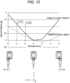
Fig. 12 , the upper part shows a graph showing a gain difference at each distance W with respect to a reference gain when the distance W is set to 0 (zero), focusing on a gain at the angle ϕ = minus 45 degrees, and the lower part shows relative positional relationsbetween theantenna body 30 and therouting structure 50 corresponding to the distances W. In the graph, a solid line indicates a case where theparasitic element 33 is "present", and a broken line indicates a case where theparasitic element 33 is "absent". - In
Figs. 10B ,11B , and12 , in the H plane, ϕ = 0 degrees in the X-axis positive direction (the forward direction) and ϕ = 90 degrees in the Y-axis positive direction (the leftward direction). - Comparing the graphs of
Figs. 10B ,11B , and12 , it can be seen that a relatively high gain is obtained when the virtual line D1 is set from the center P3 of theparasitic element 33 to a side where thefeeding point 39 is positioned even at the same distance W. For example, inFig. 12 , in a case where the distance W is 6 mm, the gain increases by about 1.9 dB when the virtual line D1 is on the Z-axis positive side. In contrast, when the virtual line D1 is on the Z-axis positive side, the gain increases by about 1.5 dB. Therefore, it is preferable to separate the virtual line D1 to the side where thefeeding point 39 is positioned than to separate the virtual line D1 to a side where thefeeding point 39 is not positioned. - When the distance W is expected to increase the gain by 0.5 dB or more compared to when the distance W is 0 (zero) at ϕ of minus 45 degrees, it can be determined that a significant effect is obtained. Therefore, according to
Fig. 12 , it is preferable that the distance W is approximately 1.8 mm or more, which is approximately λ/26 or more. - In ϕ of minus 45 degrees, it is more preferable to set a distance W at which a gain increase of about 1 dB or more is obtained compared to when the distance W is set to 0 (zero). Therefore, according to
Fig. 12 , it is more preferable that the distance W is approximately 3.7 mm or more, which is approximately λ/13 or more, at which a gain increase larger than 1 dB can be expected. -
Figs. 13 and 14 are diagrams showing a simulation result of an intensity distribution of a surface current in a steady state.Fig. 13 is a simulation result of thepatch antenna 20 of the present embodiment when the virtual line D1 is separated by a distance W of 6 mm to thefeeding point 39 side.Fig. 14 is a simulation result of a patch antenna in which the distance W is set to 0 (zero) as a comparative example. - What should be noted is the intensity of a surface current of the
parasitic element 33 on a side closer to theconnection terminal 51 and an around theparasitic element 33. The corresponding portion is shown by an ellipse of a broken line inFigs. 13 and 14 . The center P3 of theparasitic element 33 is shown by a white arrow. When the distance W is set to 6 mm, it is indicated that the surface current in the vicinity of the center of theparasitic element 33 is stronger than that of the comparative example, and the function of theparasitic element 33 is more exhibited. This indicates that when the distance W is set to 6 mm as compared with the comparative example, the directivity expandability of theparasitic element 33 acts, that is, the influence of the cable routing on the antenna characteristics can be reduced. - The
patch antenna 20 of the above embodiment may be a two-point feeding type patch antenna such as a circularly polarized patch antenna. For example, as shown inFig. 15 , anantenna body 30B includesparasitic elements 33 andparasitic elements 35 in the outside of four sides of the radiatingelement 32. Theparasitic elements 33 are disposed on a Y-axis positive direction side and a Y-axis negative direction side with respect to the radiatingelement 32 to form a pair. Theparasitic elements 35 are disposed on a Z-axis positive direction side and a negative direction side with respect to the radiatingelement 32 to form a pair. The radiatingelement 32 includes thefirst feeding point 39 and asecond feeding point 36. - The virtual line D1 is set along a Y-axis. Therefore, a distance W3 is determined in the same manner as the distance W of the above embodiment with reference to the
parasitic element 33 on the Y-axis positive direction side close to therouting structure 50 out of theparasitic elements 33. In this case, a high gain can be obtained by separating the virtual line D1 to the sides where thefeeding point 36 and thefeeding point 39 are positioned, rather than separating the virtual line D1 to a side where thefeeding point 36 or thefeeding point 39 is not positioned. - The virtual line D1 does not necessarily have to be orthogonal to a virtual line D3 in a longitudinal direction of the
parasitic element 33 in a plan view. In the plan view, the virtual line D1 may be in a direction intersecting the virtual line D3, for example, may be set to be inclined with respect to the virtual line D3. When theparasitic element 33 has a rectangular shape, the virtual line D3 represents a line (an axis) that passes through the center (the geometric center) P3 of theparasitic element 33 and connects short sides of theparasitic element 33. In other words, the virtual line D3 represents a line that passes through the center (the geometric center) P3 of theparasitic element 33 and is parallel to long sides of theparasitic element 33. - For example, an
antenna device 10C for a vehicle shown inFig. 16 includes apatch antenna 20C, abracket 11C to be attached to thewindshield 6, and acover 18. Thepatch antenna 20C includes acase 21C that accommodates an antenna body, thecable 52, and aconnector 56 provided at a distal end of thecable 52. Thecase 21C is held by a distalend holding portion 15 of thebracket 11C, and theconnector 56 is held by a rearend holding portion 16 of thebracket 11C. Thecover 18 accommodates theantenna device 10C to cover a surface other than a bonding surface to thewindshield 6. - The
patch antenna 20C basically has the same configuration as theantenna body 30 of the above embodiment, but arouting structure 50C is different from therouting structure 50 of theantenna body 30. Therouting structure 50C includes, instead of theconnection terminal 51, thecable 52 having one end fixed to thesubstrate 40, and theconnector 56 provided at the distal end of thecable 52. A fixing position of thecable 52 and thesubstrate 40 satisfies the same conditions as the conditions related to therouting structure 50 in theantenna body 30. - The virtual line D1 in the
routing structure 50C is set to form an angle of 45° with respect to the virtual line D3 in the longitudinal direction of theparasitic element 33 shown inFig. 6 in a plan view viewed from an X-axis positive direction. - An example of a method of attaching the
antenna device 10C is as follows. First, thebracket 11C is attached to thewindshield 6. Next, thepatch antenna 20C is inserted into and fixed to the distalend holding portion 15 of thebracket 11C from the side, and theconnector 56 is pressed into and fixed to the rearend holding portion 16 from the side. Finally, thecover 18 is attached to thebracket 11C along an XZ plane to slide obliquely from a front lower side to a rear upper side along thewindshield 6. - By setting the virtual line D1 obliquely with respect to the virtual line D3, a width in a Y-axis direction required for routing the
cable 52 can be reduced. When another sensor or camera is attached to thewindshield 6, if the width in the Y-axis direction can be reduced, a degree of freedom of an attachment position of theantenna device 10C increases accordingly. Setting the virtual line D1 obliquely with respect to the virtual line D3 means that an angle formed by the virtual line D1 and the virtual line D3 is an angle other than 90 degrees and 180 degrees, and includes, for example, approximately 45 degrees in a YZ plane and approximately 45 degrees in the XZ plane. - According to this attachment method, the opportunity to apply a load for pushing up the
windshield 6 from a vehicle interior side can be limited to the time of attaching thebracket 11C. In a manufacturing line of thevehicle 5, an adhesive on thewindshield 6 attached to thevehicle 5 may not be sufficiently cured. At this time, when attaching theantenna device 10C to thevehicle 5, theantenna device 10C can be attached without applying a load that excessively pushes up thewindshield 6 according to the attachment method described above. - The disclosure of the present specification including the embodiment and the modifications thereof described above can be summarized as follows.
- An aspect of the present disclosure is a patch antenna including a planar radiating element, a parasitic element provided at a position spaced apart from the radiating element in a plan view when the radiating element is viewed from a direction perpendicular to a surface of the radiating element, and a cable electrically connected to the radiating element and configured to supply power to the radiating element, in which when a direction along the cable passing through a position where the cable is electrically connected to the radiating element is defined as a cable connection direction, a virtual line in the cable connection direction is positioned away from a center of the parasitic element.
- That is, an aspect of the present disclosure is a patch antenna including a planar radiating element, a parasitic element provided at a position spaced apart from an end portion of the radiating element in a plan view when the radiating element is viewed from a direction perpendicular to a surface of the radiating element, and a cable electrically connected to the radiating element and configured to supply power to the radiating element, in which an axis of the cable passing through a position where the cable is electrically connected to the radiating element is spaced apart from a center of the parasitic element.
- According to this aspect, it is possible to implement the cable routing that has a small influence on antenna characteristics.
- A distance between the virtual line (the axis) and the center of the parasitic element may be approximately λ/26 or more, where λ is a frequency for use.
- With such a configuration, it is possible to implement the cable routing that has a small influence on antenna characteristics, and further, it is possible to increase a gain.
- A distance between the virtual line (the axis) and the center of the parasitic element may be approximately λ/13 or more, where λ is a frequency for use.
- With such a configuration, it is possible to implement the cable routing that has a small influence on antenna characteristics, and further, it is possible to increase the gain.
- The parasitic element may have a rectangular shape in the plan view, and the cable connection direction may be a direction intersecting a longitudinal direction of the parasitic element in the plan view.
- That is, the parasitic element may have a rectangular shape in the plan view, and the axis may intersect a line parallel to the longitudinal direction of the parasitic element in the plan view.
- With such a configuration, a surface current in the vicinity of the center of the parasitic element can be increased. As a result, the function as the parasitic element can be exhibited, and directivity expandability can be acted. Therefore, the influence on antenna characteristics can be reduced.
- The longitudinal direction of the parasitic element may be a direction along a line connecting a center of the radiating element and a feeding point of the radiating element in the plan view, and the virtual line (the axis) may be disposed on a side where the feeding point of the radiating element is positioned with respect to the center of the parasitic element in the plan view.
- With such a configuration, a high gain can be obtained.
- The patch antenna may further include a connection terminal that connects the cable to the radiating element.
- With such a configuration, it is possible to prevent a "prying force" from acting on an antenna body, and it is possible to prevent an adverse effect on a circuit or a joint portion of the antenna body. Further, an attachment operation is facilitated. Even if a standard of the cable is different depending on a type of a vehicle, a specification can be changed flexibly and easily by changing a type of the connection terminal.
- The parasitic element may be disposed between the connection terminal and the radiating element in the plan view.
- The patch antenna may include the cable and a connector connected to a distal end of the cable.
- The patch antenna may further include a substrate on which the radiating element and the parasitic element are provided and to which the radiating element and the cable are electrically connected, a base on which the substrate is disposed, and a case forming an accommodation space for accommodating the base, the radiating element, the parasitic element, and in which the substrate, and the case, the substrate, and the base are fastened together.
- With such a configuration, for example, it is possible to prevent abnormal noises caused by vibration or the like during traveling.
-
- 5
- vehicle
- 6
- windshield
- 10, 10C
- antenna device
- 11, 11C
- bracket
- 12
- inclined surface
- 13
- holding portion
- 15
- distal end holding portion
- 16
- rear end holding portion
- 18
- cover
- 20, 20C
- patch antenna
- 21, 21C
- case
- 22
- base
- 23
- screw
- 24
- pin
- 30, 30B
- antenna body
- 31
- dielectric
- 32
- radiating element
- 33
- parasitic element
- 34
- ground conductor
- 35
- parasitic element
- 36
- second feeding point
- 39
- first feeding point
- 40
- substrate
- 44
- radiating element
- 50, 50C
- routing structure
- 51
- connection terminal
- 52
- cable
- 52a
- connection terminal
- 56
- connector
- D1
- virtual Line (axis) in cable connection direction
- D3
- virtual line in longitudinal direction
- P1
- position
- P3
- center of parasitic element
- P4
- center of radiating element
- λ
- used frequency (communication frequency)
- ϕ
- angle
Claims (9)
- A patch antenna comprising:a planar radiating element;a parasitic element provided at a position spaced apart from an end portion of the radiating element in a plan view when the radiating element is viewed from a direction perpendicular to a surface of the radiating element; anda cable electrically connected to the radiating element and configured to supply power to the radiating element, whereinan axis of the cable passing through a position where the cable is electrically connected to the radiating element is spaced apart from a center of the parasitic element.
- The patch antenna according to claim 1, wherein
a distance between the axis and the center of the parasitic element is approximately λ/26 or more, where λ is a frequency for use. - The patch antenna according to claim 1, wherein
a distance between the axis and the center of the parasitic element is approximately λ/13 or more, where λ is a frequency for use. - The patch antenna according to any one of claims 1 to 3, whereinthe parasitic element has a rectangular shape in the plan view, andthe axis intersects a line parallel to a longitudinal direction of the parasitic element in the plan view.
- The patch antenna according to claim 4, whereinthe longitudinal direction of the parasitic element is a direction along a line connecting a center of the radiating element and a feeding point of the radiating element in the plan view, andthe axis is disposed on a side where the feeding point of the radiating element is positioned with respect to the center of the parasitic element in the plan view.
- The patch antenna according to any one of claims 1 to 5, further comprising:
a connection terminal configured to connect the cable to the radiating element. - The patch antenna according to claim 6, wherein
the parasitic element is disposed between the connection terminal and the radiating element in the plan view. - The patch antenna according to any one of claims 1 to 5, further comprising:the cable; anda connector connected to a distal end of the cable.
- The patch antenna according to any one of claims 1 to 8, further comprising:a substrate on which the radiating element and the parasitic element are provided and to which the radiating element and the cable are electrically connected;a base on which the substrate is disposed; anda case forming an accommodation space for accommodating the base, the radiating element, the parasitic element, and the substrate, whereinthe case, the substrate, and the base are fastened together.
Applications Claiming Priority (2)
| Application Number | Priority Date | Filing Date | Title |
|---|---|---|---|
| JP2020162325 | 2020-09-28 | ||
| PCT/JP2021/035401 WO2022065489A1 (en) | 2020-09-28 | 2021-09-27 | Patch antenna |
Publications (2)
| Publication Number | Publication Date |
|---|---|
| EP4220855A1 true EP4220855A1 (en) | 2023-08-02 |
| EP4220855A4 EP4220855A4 (en) | 2024-11-06 |
Family
ID=80846743
Family Applications (1)
| Application Number | Title | Priority Date | Filing Date |
|---|---|---|---|
| EP21872615.6A Pending EP4220855A4 (en) | 2020-09-28 | 2021-09-27 | Patch antenna |
Country Status (5)
| Country | Link |
|---|---|
| US (1) | US20230291107A1 (en) |
| EP (1) | EP4220855A4 (en) |
| JP (3) | JP7490070B2 (en) |
| CN (1) | CN116210126A (en) |
| WO (1) | WO2022065489A1 (en) |
Families Citing this family (5)
| Publication number | Priority date | Publication date | Assignee | Title |
|---|---|---|---|---|
| CN118355562A (en) * | 2021-12-03 | 2024-07-16 | Agc株式会社 | Antenna device and vehicle antenna device |
| WO2023112866A1 (en) * | 2021-12-14 | 2023-06-22 | Agc株式会社 | Antenna device with attachment member and attachment structure for antenna device |
| JPWO2023127765A1 (en) * | 2021-12-28 | 2023-07-06 | ||
| KR102890235B1 (en) * | 2022-03-28 | 2025-11-24 | 주식회사 에이치엘클레무브 | Microstrip antenna and radar device for vehicle including the same |
| KR20250008313A (en) * | 2023-07-07 | 2025-01-14 | 현대자동차주식회사 | Antenna apparatus and vehicl including the same |
Family Cites Families (15)
| Publication number | Priority date | Publication date | Assignee | Title |
|---|---|---|---|---|
| AUPQ204599A0 (en) * | 1999-08-05 | 1999-08-26 | R F Industries Pty Ltd | Dual band antenna |
| JP4541595B2 (en) * | 2001-06-18 | 2010-09-08 | マスプロ電工株式会社 | Microstrip antenna |
| JP2003257554A (en) * | 2002-02-28 | 2003-09-12 | Molex Inc | Thin antenna |
| JP4115428B2 (en) * | 2004-06-25 | 2008-07-09 | アルプス電気株式会社 | In-vehicle antenna device |
| JP5005229B2 (en) * | 2005-02-08 | 2012-08-22 | 八木アンテナ株式会社 | Bidirectional beam antenna and transmission system |
| JP4208025B2 (en) * | 2006-07-12 | 2009-01-14 | Toto株式会社 | High frequency sensor device |
| JP4659723B2 (en) * | 2006-11-30 | 2011-03-30 | ミツミ電機株式会社 | Antenna device |
| CN101308957A (en) * | 2008-06-13 | 2008-11-19 | 航天恒星科技股份有限公司 | Circularly Polarized Broadband Capacitance-Compensated Probe-fed Laminated Microstrip Antenna Array |
| CN103490151B (en) * | 2013-08-30 | 2015-08-26 | 大连海事大学 | A L-Band Broadband Circularly Polarized Microstrip Antenna |
| CN104103897B (en) * | 2014-08-01 | 2016-08-24 | 重庆大学 | A kind of compact ultra-wideband antenna based on L-type parasitism band |
| CN106299661A (en) * | 2016-09-19 | 2017-01-04 | 中国电子科技集团公司第二十研究所 | A kind of miniaturization navigation reception antenna |
| JP6971119B2 (en) | 2017-10-13 | 2021-11-24 | 株式会社ヨコオ | Patch antenna and in-vehicle antenna device |
| US20200373666A1 (en) * | 2018-02-14 | 2020-11-26 | Hitachi Metals, Ltd. | Multiband antenna, wireless communication module, and wireless communication device |
| WO2019163521A1 (en) | 2018-02-23 | 2019-08-29 | 株式会社ヨコオ | Patch antenna and vehicle-mounted antenna device |
| CN213026503U (en) * | 2019-06-26 | 2021-04-20 | 株式会社友华 | Composite antenna device |
-
2021
- 2021-09-27 JP JP2022552104A patent/JP7490070B2/en active Active
- 2021-09-27 EP EP21872615.6A patent/EP4220855A4/en active Pending
- 2021-09-27 WO PCT/JP2021/035401 patent/WO2022065489A1/en not_active Ceased
- 2021-09-27 US US18/028,793 patent/US20230291107A1/en active Pending
- 2021-09-27 CN CN202180065967.6A patent/CN116210126A/en active Pending
-
2024
- 2024-01-29 JP JP2024010656A patent/JP7550328B2/en active Active
- 2024-01-29 JP JP2024010657A patent/JP7542764B2/en active Active
Also Published As
| Publication number | Publication date |
|---|---|
| JP7550328B2 (en) | 2024-09-12 |
| JP7542764B2 (en) | 2024-08-30 |
| CN116210126A (en) | 2023-06-02 |
| JP2024042040A (en) | 2024-03-27 |
| JP2024042041A (en) | 2024-03-27 |
| WO2022065489A1 (en) | 2022-03-31 |
| US20230291107A1 (en) | 2023-09-14 |
| EP4220855A4 (en) | 2024-11-06 |
| JP7490070B2 (en) | 2024-05-24 |
| JPWO2022065489A1 (en) | 2022-03-31 |
Similar Documents
| Publication | Publication Date | Title |
|---|---|---|
| US20230291107A1 (en) | Patch antenna | |
| US10854950B2 (en) | Antenna device | |
| CN100530820C (en) | Defferential-fed stacked patch antenna | |
| US11476565B2 (en) | Patch antenna and antenna device for vehicle | |
| EP2888133B1 (en) | Vehicle camera with integrated hf antenna and motor vehicle | |
| JPWO2019116941A1 (en) | Antenna devices, antenna modules, and wireless devices | |
| US20060017646A1 (en) | Transceiver-integrated antenna | |
| JP2009124403A (en) | Antenna device | |
| WO2012008177A1 (en) | Antenna device | |
| JP2007074226A (en) | Vehicle-mounted antenna system | |
| US7259722B2 (en) | Antenna coupler and mount for mobile radio terminals | |
| US12620713B2 (en) | Patch antenna and antenna device | |
| US10535915B2 (en) | Antenna module and transceiver | |
| JP7845378B2 (en) | Antenna device with mounting components and mounting structure for the antenna device | |
| US20250239821A1 (en) | Connector, connector set, and connector-equipped cable | |
| EP3517828A1 (en) | Automotive lighting module and automotive lighting device | |
| WO2024116430A1 (en) | Antenna device | |
| US20240347899A1 (en) | Antenna device and vehicle antenna device | |
| JP7264277B2 (en) | Electronics | |
| US20240322435A1 (en) | Antenna device and vehicle antenna device | |
| JP3804924B2 (en) | Planar antenna | |
| WO2022210828A1 (en) | Antenna device | |
| JP2022159131A (en) | antenna device | |
| WO2025192069A1 (en) | Antenna device | |
| JPH0946118A (en) | GPS receiver |
Legal Events
| Date | Code | Title | Description |
|---|---|---|---|
| STAA | Information on the status of an ep patent application or granted ep patent |
Free format text: STATUS: THE INTERNATIONAL PUBLICATION HAS BEEN MADE |
|
| PUAI | Public reference made under article 153(3) epc to a published international application that has entered the european phase |
Free format text: ORIGINAL CODE: 0009012 |
|
| STAA | Information on the status of an ep patent application or granted ep patent |
Free format text: STATUS: REQUEST FOR EXAMINATION WAS MADE |
|
| 17P | Request for examination filed |
Effective date: 20230327 |
|
| AK | Designated contracting states |
Kind code of ref document: A1 Designated state(s): AL AT BE BG CH CY CZ DE DK EE ES FI FR GB GR HR HU IE IS IT LI LT LU LV MC MK MT NL NO PL PT RO RS SE SI SK SM TR |
|
| DAV | Request for validation of the european patent (deleted) | ||
| DAX | Request for extension of the european patent (deleted) | ||
| A4 | Supplementary search report drawn up and despatched |
Effective date: 20241007 |
|
| RIC1 | Information provided on ipc code assigned before grant |
Ipc: H01Q 19/00 20060101ALI20240930BHEP Ipc: H01Q 5/378 20150101ALI20240930BHEP Ipc: H01Q 1/12 20060101ALI20240930BHEP Ipc: H01Q 9/04 20060101ALI20240930BHEP Ipc: H01Q 1/32 20060101AFI20240930BHEP |