EP4220700A1 - Method for manufacturing memory - Google Patents
Method for manufacturing memory Download PDFInfo
- Publication number
- EP4220700A1 EP4220700A1 EP21941549.4A EP21941549A EP4220700A1 EP 4220700 A1 EP4220700 A1 EP 4220700A1 EP 21941549 A EP21941549 A EP 21941549A EP 4220700 A1 EP4220700 A1 EP 4220700A1
- Authority
- EP
- European Patent Office
- Prior art keywords
- layer
- core region
- mask
- mask layer
- bit line
- Prior art date
- Legal status (The legal status is an assumption and is not a legal conclusion. Google has not performed a legal analysis and makes no representation as to the accuracy of the status listed.)
- Granted
Links
Images






Classifications
-
- H—ELECTRICITY
- H10—SEMICONDUCTOR DEVICES; ELECTRIC SOLID-STATE DEVICES NOT OTHERWISE PROVIDED FOR
- H10B—ELECTRONIC MEMORY DEVICES
- H10B12/00—Dynamic random access memory [DRAM] devices
- H10B12/30—DRAM devices comprising one-transistor - one-capacitor [1T-1C] memory cells
- H10B12/48—Data lines or contacts therefor
- H10B12/485—Bit line contacts
-
- H—ELECTRICITY
- H10—SEMICONDUCTOR DEVICES; ELECTRIC SOLID-STATE DEVICES NOT OTHERWISE PROVIDED FOR
- H10B—ELECTRONIC MEMORY DEVICES
- H10B12/00—Dynamic random access memory [DRAM] devices
- H10B12/01—Manufacture or treatment
- H10B12/09—Manufacture or treatment with simultaneous manufacture of the peripheral circuit region and memory cells
-
- H—ELECTRICITY
- H10—SEMICONDUCTOR DEVICES; ELECTRIC SOLID-STATE DEVICES NOT OTHERWISE PROVIDED FOR
- H10B—ELECTRONIC MEMORY DEVICES
- H10B12/00—Dynamic random access memory [DRAM] devices
- H10B12/50—Peripheral circuit region structures
-
- H—ELECTRICITY
- H10—SEMICONDUCTOR DEVICES; ELECTRIC SOLID-STATE DEVICES NOT OTHERWISE PROVIDED FOR
- H10P—GENERIC PROCESSES OR APPARATUS FOR THE MANUFACTURE OR TREATMENT OF DEVICES COVERED BY CLASS H10
- H10P50/00—Etching of wafers, substrates or parts of devices
- H10P50/20—Dry etching; Plasma etching; Reactive-ion etching
- H10P50/28—Dry etching; Plasma etching; Reactive-ion etching of insulating materials
- H10P50/286—Dry etching; Plasma etching; Reactive-ion etching of insulating materials of organic materials
- H10P50/287—Dry etching; Plasma etching; Reactive-ion etching of insulating materials of organic materials by chemical means
-
- H—ELECTRICITY
- H10—SEMICONDUCTOR DEVICES; ELECTRIC SOLID-STATE DEVICES NOT OTHERWISE PROVIDED FOR
- H10P—GENERIC PROCESSES OR APPARATUS FOR THE MANUFACTURE OR TREATMENT OF DEVICES COVERED BY CLASS H10
- H10P76/00—Manufacture or treatment of masks on semiconductor bodies, e.g. by lithography or photolithography
- H10P76/20—Manufacture or treatment of masks on semiconductor bodies, e.g. by lithography or photolithography of masks comprising organic materials
- H10P76/204—Manufacture or treatment of masks on semiconductor bodies, e.g. by lithography or photolithography of masks comprising organic materials of organic photoresist masks
- H10P76/2041—Photolithographic processes
- H10P76/2043—Photolithographic processes using an anti-reflective coating
-
- H—ELECTRICITY
- H10—SEMICONDUCTOR DEVICES; ELECTRIC SOLID-STATE DEVICES NOT OTHERWISE PROVIDED FOR
- H10B—ELECTRONIC MEMORY DEVICES
- H10B12/00—Dynamic random access memory [DRAM] devices
- H10B12/30—DRAM devices comprising one-transistor - one-capacitor [1T-1C] memory cells
- H10B12/34—DRAM devices comprising one-transistor - one-capacitor [1T-1C] memory cells the transistor being at least partially in a trench in the substrate
Definitions
- the present application relates to the technical field of semiconductors, and in particular, to a manufacturing method of a memory.
- a DRAM dynamic random access memory
- a DRAM usually includes a plurality of memory cells.
- Each memory cell includes a transistor and a capacitor.
- a gate of the transistor is electrically connected to a word line
- a source of the transistor is electrically connected to a bit line
- a drain of the transistor is electrically connected to the capacitor.
- a word line voltage on the word line can control on or off of the transistor, such that data information stored in the capacitor can be read through the bit line or data information can be written to the capacitor.
- a void or a seam is easily formed within a bit line contact, resulting in performance degradation of the memory.
- Embodiments of the present application provide a manufacturing method of a memory, where the manufacturing method includes: providing a substrate, where the substrate includes a core region and a peripheral region located outside the core region, a plurality of active regions are arranged at intervals in the core region, and a first barrier layer is further provided in the core region; laminating and forming a first conductive layer and a first mask layer on the substrate in sequence; etching the first mask layer, the first conductive layer, and the first barrier layer which are in the core region, to form a first etched hole penetrating through the first mask layer, the first conductive layer, and the first barrier layer, where the first etched hole is opposite to the active region; etching the substrate along the first etched hole, to form a bit line contact hole, where the bit line contact hole exposes the active region; removing the first mask layer and the first conductive layer which are in the core region and located around the bit line contact hole, and retaining the first barrier layer located around the bit line contact hole; and forming a bit
- a bit line contact 410 is formed in the second conductive layer 400 located in a bit line contact hole, and a void or a seam easily occurs in the bit line contact 410. As shown by dotted lines in FIG. 1 , the void or the seam affects performance of the bit line contact 410, resulting in performance degradation of a memory.
- an embodiment of the present application provides a manufacturing method of a memory.
- a first mask layer and a first conductive layer around a bit line contact hole in a core region are removed, such that a total depth of a first etched hole and the bit line contact hole is reduced, thereby reducing a formation height of a bit line contact, reducing or even avoiding formation of a void or a seam in the bit line contact, improving a capability of the bit line contact to transmit a charge, and improving performance of the memory.
- FIG. 2 shows a procedure of a manufacturing method of a memory according to an embodiment of the present application.
- the manufacturing method includes the following steps: Step S101. Provide a substrate, where the substrate includes a core region and a peripheral region located outside the core region, a plurality of active regions are arranged at intervals in the core region, and a first barrier layer is further provided in the core region.
- the substrate includes a core region and a peripheral region, a memory cell (for example, a capacitor) array is formed in the core region to store data information; and a peripheral logic circuit is formed in the peripheral region to control writing or reading of data information.
- a memory cell for example, a capacitor
- the peripheral region is provided outside the core region.
- the peripheral region is provided at a circumferential edge of the core region, that is, the peripheral region is provided around the core region.
- the core region is shown by A in FIG. 3
- the peripheral region is shown by B in FIG. 3
- the peripheral region and the core region may be adjacent to each other.
- a plurality of active regions are arranged at intervals in the core region 110, and a shallow trench isolation (STI) structure 120 is provided between active regions 110.
- the shallow trench isolation structure 120 is filled with an insulating material, such as silicon oxide or silicon oxynitride, so as to isolate the active regions 110 from each other.
- a buried word line (BWL) 130 may be further provided in the core region.
- the peripheral region may also be provided with active regions 110. As shown in FIG. 3 , a spacing between the active regions 110 located in the core region is relatively small, and a spacing between the active regions 110 located in the peripheral region is relatively large. That is, the active regions 110 in the core region are denser, and the active regions 110 located in the peripheral region are sparser.
- a first barrier layer 140 is further provided in the core region, and the first barrier layer 140 further insulates and protects the core region.
- a material of the first barrier layer 140 may be silicon nitride.
- the first barrier layer 140 is deposited and formed in the core region. As shown in FIG. 3 , the first barrier layer 140 is not provided in the peripheral region.
- Step S102 Laminate and form a first conductive layer and a first mask layer on the substrate in sequence.
- a first conductive layer 200 is formed on the substrate, where the first conductive layer 200 covers the core region and the peripheral region, and then a first mask layer 300 is formed on the first conductive layer 200, where the first mask layer 300 covers the first conductive layer 200.
- the first conductive layer 200 and the first mask layer 300 are laminated.
- a material of the first conductive layer 200 may be polycrystalline silicon, and a material of the first mask layer 300 may be oxide, such as silicon oxide.
- a thickness of the first mask layer 300 is greater than or equal to 10 nm.
- the thickness of the first mask layer 300 may be reduced, such that the first mask layer 300 is easy to remove subsequently while protecting the first conductive layer 200.
- the first conductive layer 200 and the first mask layer 300 may be formed through a deposition process.
- the first conductive layer 200 and the first mask layer 300 are formed through chemical vapor deposition (CVD), physical vapor deposition (PVD), or atomic layer deposition (ALD).
- CVD chemical vapor deposition
- PVD physical vapor deposition
- ALD atomic layer deposition
- Step S103 Etch the first mask layer, the first conductive layer, and the first barrier layer in the core region, to form a first etched hole penetrating through the first mask layer, the first conductive layer, and the first barrier layer, where the first etched hole is opposite to the active region.
- part of the first mask layer 300, part of the first conductive layer 200, and part of the first barrier layer 140 in the core region are removed, to form a first etched hole 310, where the first etched hole 310 runs through the first mask layer 300, the first conductive layer 200, and the first barrier layer 140.
- the first etched hole 310 is opposite to the active region 110.
- an orthographic projection of the first etched hole 310 on the active region 110 covers part of a surface of the active region 110, for example, covers a central region of an upper surface of the active region 110.
- Step S104 Etch the substrate along the first etched hole, to form a bit line contact hole, where the bit line contact hole exposes the active region.
- the substrate is etched along the first etched hole 310, to form a bit line contact hole 150 in the core region.
- the bit line contact hole 150 exposes the active region 110, that is, at least part of a hole bottom of the bit line contact hole 150 is the active region 110.
- Step S105 Remove the first mask layer and the first conductive layer in the core region and located around the bit line contact hole, and retain the first barrier layer located around the bit line contact hole.
- the first mask layer 300 and the first conductive layer 200 in the core region are removed, and the first barrier layer 140 in the core region is retained.
- the first barrier layer 140 is exposed in the core region, and after the first mask layer 300 and the first conductive layer 200 in the core region are removed, a thickness of a film layer on the substrate is reduced, that is, a depth of the first etched hole 310 is reduced, such that a total depth of the first etched hole 310 and the bit line contact hole 150 is reduced, thereby facilitating subsequent formation of a better-quality bit line contact 410.
- Step S106 Form a bit line contact in the bit line contact hole, where the bit line contact is electrically connected to the active region, and a surface of the bit line contact away from the substrate is flush with a surface of the first barrier layer away from the substrate.
- a bit line contact 410 is formed in the bit line contact hole 150, and the bit line contact 410 is in contact with the active region 110, such that the bit line contact 410 is electrically connected to the active region 110.
- the surface of the bit line contact 410 away from the substrate is flush with a surface of the first barrier layer 140 away from the substrate.
- an upper surface of the bit line contact 410 is flush with an upper surface of the first barrier layer 140, such that other relatively flat film layers are formed on the bit line contact 410 and on the first barrier layer 140.
- the first mask layer 300 and the first conductive layer 200 located around the bit line contact hole 150 in the core region are removed, such that a formation height of the bit line contact 410 is reduced and formation quality of the bit line contact 410 is good, thereby reducing generation of a void and/or a seam due to uneven filling of the bit line contact 410, improving a capability of the bit line contact 410 to transmit a charge, and improving performance of the memory.
- the step of forming a bit line contact 410 in the bit line contact hole 150 includes: referring to FIG. 9 and FIG. 10 , depositing a second conductive layer 400 in the bit line contact hole 150, on the first barrier layer 140 in the core region, and on the first mask layer 300 in the peripheral region. As shown in FIG. 9 and FIG. 10 , the second conductive layer 400 fills the bit line contact hole 150, and covers the first barrier layer 140 in the core region and the first mask layer 300 in the peripheral region.
- the second conductive layer 400 also fills the remaining first etched hole 310, that is, the second conductive layer 400 fills the first etched hole 310 between the first barrier layers 140.
- a material of the second conductive layer 400 may be polycrystalline silicon, such as doped polysilicon or non-doped polysilicon.
- the material of the second conductive layer 400 is not limited.
- the material of the second conductive layer 400 may alternatively be a metal conductive material.
- the second conductive layer 400 on the first barrier layer 140 in the core region and the second conductive layer 400 in the peripheral region are etched and removed.
- the first barrier layer 140 in the core region is used as an etching stop layer, part of the second conductive layer 400 is etched and removed, and the second conductive layer 400 located in the bit line contact hole 150 is retained, and the retained second conductive layer 400 is flush with the first barrier layer 140.
- the second conductive layer 400 is etched back after the deposition of the second conductive layer 400, to form the bit line contact 410. As shown in FIG. 11 , the first barrier layer 140 is exposed in the core region, and the first conductive layer 200 is exposed in the peripheral region.
- a thickness of a film layer on the substrate is reduced, and a depth of a hole to be filled by the second conductive layer 400 is reduced, such that deposition difficulty of the second conductive layer 400 in the bit line contact hole 150 is reduced, and deposition quality is good, thereby reducing or even avoiding formation of a void or a seam in the second conductive layer 400 in the bit line contact hole 150, that is, reducing or even avoiding occurrence of a void or a seam in the bit line contact 410, and improving formation quality of the bit line contact 410.
- the first mask layer 300 in the peripheral region is etched and removed, to expose the first conductive layer 200 in the peripheral region.
- the first mask layer 300 in the peripheral region is removed through wet etching.
- the bit line contact 410 is formed in the core region, and the first conductive layer 200 is exposed in the peripheral region.
- the manufacturing method of a memory in this embodiment of the present application includes: providing a substrate, where the substrate includes a core region and a peripheral region located outside the core region, a plurality of active regions 110 are arranged at intervals in the core region, and a first barrier layer 140 is further provided in the core region; laminating and forming a first conductive layer 200 and a first mask layer 300 on the substrate in sequence; etching the first mask layer 300, the first conductive layer 200, and the first barrier layer 140 in the core region, to form a first etched hole 310, where the first etched hole 310 is opposite to the active region 110; etching the substrate along the first etched hole 310, to form a bit line contact hole 150, where the bit line contact hole 150 exposes the active region 110; removing the first mask layer 300 and the first conductive layer 200 in the core region and located around the bit line contact hole 150, and retaining the first barrier layer 140 located around the bit line contact hole 150; and forming a bit line contact 410 in the bit line contact hole 150
- the removal of the first mask layer 300 and the first conductive layer 200 around the bit line contact hole 150 in the core region reduces a total depth of the first etched hole 310 and the bit line contact hole 150, such that during subsequent formation of the bit line contact 410, the surface of the bit line contact 410 away from the substrate is flush with the surface of the first barrier layer 140 away from the substrate.
- a formation height of the bit line contact 410 is reduced, thereby reducing or even avoiding formation of a void or a seam in the bit line contact 410, that is, improving formation quality of the bit line contact 410, improving a capability of the bit line contact 410 to transmit a charge, and improving performance of the memory.
- the manufacturing method of a memory further includes: Step S201. Laminate and form a second mask layer, a third mask layer, and an intermediate layer on the first mask layer in sequence, where the third mask layer in the core region has a filling hole penetrating through the third mask layer, and part of the intermediate layer is located in the filling hole.
- a second mask layer 500 is formed on the first mask layer 300
- a third mask layer 600 is formed on the second mask layer 500
- an intermediate layer 700 is formed on the third mask layer 600.
- the first mask layer 300, the second mask layer 500, the third mask layer 600, and the intermediate layer 700 form a stacked structure, and all the four film layers are located on the core region and the peripheral region.
- the third mask layer 600 in the core region has a filling hole, and the filling hole runs through the third mask layer 600, that is, a hole bottom of the filling hole is the second mask layer 500.
- the filling hole is opposite to the active region 110.
- an orthographic projection of the filling hole on the active region 110 covers part of a surface of the active region 110 facing away from the substrate.
- Part of the intermediate layer 700 is located in the filling hole, and part of the intermediate layer 700 is located on the third mask layer 600, that is, part of the intermediate layer 700 is located in the third mask layer 600, and part of the intermediate layer 700 is located outside the third mask layer 600.
- the intermediate layer 700 located in the filling hole is subsequently used as a mask for the bit line contact hole 150.
- a material of the intermediate layer 700 may be oxide.
- the step of laminating and forming a second mask layer 500, a third mask layer 600, and an intermediate layer 700 on the first mask layer 300 in sequence may include: depositing the second mask layer 500 and the third mask layer 600 on the first mask layer 300 in sequence, that is, depositing the second mask layer 500 on the first mask layer 300, and depositing the third mask layer 600 on the second mask layer 500; etching and removing part of the third mask layer 600 in the core region, to form the filling hole; and depositing the intermediate layer 700 in the filling hole and on the third mask layer 600.
- a deposition thickness of the intermediate layer 700 is greater than a thickness of the third mask layer 600 and may be less than a preset value, that is, a total height of the intermediate layer 700 along a direction facing away from the substrate is less than a preset value, and the intermediate layer 700 may be removed at the same time with etching of a film layer below the intermediate layer 700 when the intermediate layer 700 is used as a mask.
- Step S202 Remove part of the intermediate layer in the core region and the third mask layer in the core region, and retain the intermediate layer located in the filling hole.
- the intermediate layer 700 located in the filling hole is retained, the remaining intermediate layer 700 in the core region is etched and removed, and the third mask layer 600 in the core region is etched and removed.
- the second mask layer 500 is exposed between intermediate layers 700 retained in the core region, and the intermediate layer 700 is exposed in the peripheral region.
- the removing the third mask layer 600 in the core region and part of the intermediate layer 700 in the core region, and retaining the intermediate layer 700 located in the filling hole may include: referring to FIG. 14 , depositing a photoresist layer 800 on the intermediate layer 700 in the peripheral region, where the photoresist layer 800 covers the intermediate layer 700. As shown in FIG. 14 , the photoresist layer 800 covers the intermediate layer 700 in the peripheral region, and the photoresist layer 800 does not cover the intermediate layer 700 in the core region, that is, the intermediate layer 700 in the core region is exposed.
- the intermediate layer 700 on the third mask layer 600 in the core region is etched and removed by taking the photoresist layer 800 as a mask.
- the third mask layer 600 is used as an etching stop layer, the intermediate layer 700 is etched, the intermediate layer 700 covered by the photoresist layer 800 is retained, and the intermediate layer 700 not covered by the photoresist layer 800 and located on the third mask layer 600 is removed.
- the third mask layer 600 in the core region and the photoresist layer 800 in the peripheral region are etched and removed, the second mask layer 500 is exposed in the core region, and the intermediate layer 700 is exposed in the peripheral region.
- the third mask layer 600 includes a first base layer 610 located on the second mask layer 500, and a first anti-reflection layer 620 located on the first base layer 610.
- a material of the first anti-reflection layer 620 may be silicon oxynitride.
- a material of the first base layer 610 may be spin-on carbon (SOC).
- the step of etching and removing the third mask layer 600 in the core region and the photoresist layer 800 in the peripheral region, to expose the second mask layer 500 in the core region and the intermediate layer 700 in the peripheral region includes: etching and removing the first anti-reflection layer 620 in the core region, to expose the first base layer 610 in the core region. As shown in FIG.
- the first base layer 610 is used as an etching stop layer, the first anti-reflection layer 620 is etched, to remove the first anti-reflection layer 620 in the core region, and none of the intermediate layer 700 in the peripheral region and the first anti-reflection layer 620 are etched.
- the intermediate layer 700 on the first base layer 610 in the core region is also removed, that is, the first base layer 610 in the core region is flush with the intermediate layer 700 in the core region.
- the first base layer 610 in the core region and the photoresist layer 800 in the peripheral region are etched and removed at the same time. As shown in FIG. 17 , the first base layer 610 in the core region and the photoresist layer 800 in the peripheral region are removed in a same etching process.
- an etch selectivity ratio of the first base layer 610 to the intermediate layer 700 is greater than or equal to 50, a first etchant is oxygen (O 2 ), a first etching frequency is 60 MHz, and a first etching power is 1000 W to 1200 W.
- a first etchant is oxygen (O 2 )
- a first etching frequency is 60 MHz
- a first etching power is 1000 W to 1200 W.
- the intermediate layer 700 is retained in the core region, and the intermediate layer 700 is retained in the peripheral region, such that in a subsequent etching process, the intermediate layer 700 in the core region and the intermediate layer 700 in the peripheral region can be removed at the same time.
- film layers in the core region and in the peripheral region have a good correspondence, such that the core region and the peripheral region can be etched at the same time, thereby improving manufacturing efficiency of the memory.
- the second mask layer 500 in the core region and the third mask layer 600 in the peripheral region can be processed at the same time.
- Step S203 Etch and remove, by taking the retained intermediate layer as a mask, the second mask layer exposed in the core region.
- a pattern of the intermediate layer 700 in the core region is transferred to the second mask layer 500, and the etched second mask layer 500 can continue to transfer the pattern to the first mask layer 300, the first conductive layer 200, and the first barrier layer 140, to facilitate subsequent formation of the first etched hole 310 in the first mask layer 300, the first conductive layer 200, and the first barrier layer 140.
- an etch selectivity ratio of the second mask layer 500 to the intermediate layer 700 is adjusted, such that the intermediate layer 700 in the peripheral region is removed while the second mask layer 500 exposed in the core region is removed. It can be understood that, the intermediate layer 700 in the core region is also partially removed.
- the second mask layer 500 includes a second base layer 510 located on the first mask layer 300, and a second anti-reflection layer 520 located on the second base layer 510.
- a material of the second base layer 510 is SOC
- a material of the second anti-reflection layer 520 is silicon oxynitride.
- the etching and removing, by taking the retained intermediate layer 700 as a mask, the second mask layer 500 exposed in the core region may specifically include: referring to FIG. 18 , etching and removing the second anti-reflection layer 520 exposed in the core region, and etching and removing part of the intermediate layer 700 in the core region and the entire intermediate layer 700 in the peripheral region.
- the second base layer 510 is exposed in the core region
- the third mask layer 600 is exposed in the peripheral region.
- An etch selectivity ratio of the intermediate layer 700 to the second anti-reflection layer 520 is 1, and a thickness of the intermediate layer 700 in the peripheral region is greater than a thickness of the second anti-reflection layer 520 and less than 1.2 to 1.3 times a thickness of the second anti-reflection layer 520, that is, a thickness of the part of the intermediate layer 700 located on the third mask layer 600 is greater than a thickness of the second anti-reflection layer 520 and less than 1.2 to 1.3 times a thickness of the second anti-reflection layer 520, such that the intermediate layer 700 is etched while the second anti-reflection layer 520 is etched.
- a second etchant includes sulfur hexafluoride (SF 6 ) and difluoromethane (CH 2 F 2 ), and a diluent is nitrogen (N 2 ) or helium (He).
- SF 6 sulfur hexafluoride
- CH 2 F 2 difluoromethane
- a diluent is nitrogen (N 2 ) or helium (He).
- the second etchant is not limited, and the second etchant may alternatively be other organic compounds or mixtures containing fluorocarbons.
- the second base layer 510 is etched by taking the remaining intermediate layer 700 as a mask, to remove the exposed second base layer 510. As shown in FIG. 19 , the first mask layer 300 is exposed in the core region, and the third mask layer 600 is exposed in the peripheral region.
- the third mask layer 600 includes a first base layer 610 and a first anti-reflection layer 620, where the first base layer 610 is located on the second mask layer 500, and the first anti-reflection layer 620 is located on the first base layer 610.
- the second mask layer 500 includes a second base layer 510 and a second anti-reflection layer 520
- the third mask layer 600 includes a first base layer 610 and a first anti-reflection layer 620.
- a thickness of the second base layer 510 is greater than or equal to 1.3 to 1.5 times a thickness of the first base layer 610.
- An etch selectivity ratio of the second base layer 510 to the first anti-reflection layer 620 is greater than or equal to 20.
- a fourth etchant may be a mixture of sulfur dioxide (SO 2 ) and oxygen, to etch the second base layer 510 while retaining at least part of the first anti-reflection layer 620 in the peripheral region.
- the entire intermediate layer 700 can be removed while the second anti-reflection layer 520 exposed in the core region is etched and removed, that is, the entire intermediate layer 700 in the core region and the entire intermediate layer 700 in the peripheral region are etched and removed.
- a film layer below the intermediate layer 700 in the core region is used as a mask to transfer a pattern during subsequent etching.
- the second anti-reflection layer 520 is used as a mask during the etching of the second base layer 510.
- the step of removing the first mask layer 300 and the first conductive layer 200 in the core region and located around the bit line contact hole 150, and retaining the first barrier layer 140 located around the bit line contact hole 150 includes: etching the first mask layer 300, the first conductive layer 200, and the first barrier layer 140 by taking the remaining intermediate layer 700 as a mask, to form the first etched hole 310.
- the remaining intermediate layer 700 is used as a mask to continue to etch the first mask layer 300, the first conductive layer 200, and the first barrier layer 140, to form the first etched hole 310 in the core region.
- the manufacturing method of a memory further includes: referring to FIG. 21 , removing the remaining intermediate layer 700, the remaining second anti-reflection layer 520 in the core region, and the first anti-reflection layer 620 in the peripheral region.
- the second base layer 510 is exposed in the core region, and the first base layer 610 is exposed in the peripheral region, such that the first base layer 610 and the second base layer 510 can be subsequently removed at the same time.
- the remaining second base layer 510 in the core region and the first base layer 610 in the peripheral region are removed at the same time.
- an etch selectivity ratio of the first base layer 610 to the first mask layer 300 is greater than or equal to 50
- an etch selectivity ratio of the first base layer 610 to the second anti-reflection layer 520 is greater than or equal to 50.
- a third etchant is oxygen
- a second etching frequency is 60 MHz
- a second etching power is 1000 W to 1200 W.
- the step of removing the first mask layer 300 and the first conductive layer 200 in the core region and located around the bit line contact hole 150, and retaining the first barrier layer 140 located around the bit line contact hole 150 further includes: removing the remaining first mask layer 300 and the remaining first conductive layer 200 in the core region, and removing the second anti-reflection layer 520 in the peripheral region; and removing the second base layer 510 in the peripheral region, to expose the first mask layer 300 in the peripheral region.
- both the remaining first mask layer 300 in the core region and the remaining first conductive layer 200 in the core region are removed, and the first barrier layer 140 is exposed in the core region.
- the second anti-reflection layer 520 in the peripheral region is also removed, and the second base layer 510 is exposed in the peripheral region.
- the first mask layer 300 in the core region, the first conductive layer 200 in the core region, and the second anti-reflection layer 520 in the peripheral region may be removed in this step.
- the first mask layer 300 in the core region, the first conductive layer 200 in the core region, and the second anti-reflection layer 520 in the peripheral region are etched and removed while the substrate is etched along the first etched hole 310 to form the bit line contact hole 150.
- the second base layer 510 in the peripheral region is removed through wet etching.
Landscapes
- Engineering & Computer Science (AREA)
- Manufacturing & Machinery (AREA)
- Semiconductor Memories (AREA)
- Internal Circuitry In Semiconductor Integrated Circuit Devices (AREA)
Abstract
Description
- The present application claims the priority to
Chinese Patent Application No. 202110527256.8, titled "MANUFACTURING METHOD OF MEMORY", filed to the China National Intellectual Property Administration on May 14, 2021 - The present application relates to the technical field of semiconductors, and in particular, to a manufacturing method of a memory.
- With gradual development of storage device technologies, a dynamic random access memory (DRAM) is widely used in various electronic devices due to its high density and fast reading/writing speed. A DRAM usually includes a plurality of memory cells. Each memory cell includes a transistor and a capacitor. A gate of the transistor is electrically connected to a word line, a source of the transistor is electrically connected to a bit line, and a drain of the transistor is electrically connected to the capacitor. A word line voltage on the word line can control on or off of the transistor, such that data information stored in the capacitor can be read through the bit line or data information can be written to the capacitor.
- During manufacturing of a memory, a void or a seam is easily formed within a bit line contact, resulting in performance degradation of the memory.
- Embodiments of the present application provide a manufacturing method of a memory, where the manufacturing method includes: providing a substrate, where the substrate includes a core region and a peripheral region located outside the core region, a plurality of active regions are arranged at intervals in the core region, and a first barrier layer is further provided in the core region; laminating and forming a first conductive layer and a first mask layer on the substrate in sequence; etching the first mask layer, the first conductive layer, and the first barrier layer which are in the core region, to form a first etched hole penetrating through the first mask layer, the first conductive layer, and the first barrier layer, where the first etched hole is opposite to the active region; etching the substrate along the first etched hole, to form a bit line contact hole, where the bit line contact hole exposes the active region; removing the first mask layer and the first conductive layer which are in the core region and located around the bit line contact hole, and retaining the first barrier layer located around the bit line contact hole; and forming a bit line contact in the bit line contact hole, where the bit line contact is electrically connected to the active region, and a surface of the bit line contact away from the substrate is flush with a surface of the first barrier layer away from the substrate.
-
-
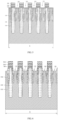
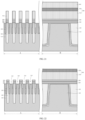
FIG. 1 is a schematic structural diagram after formation of a bit line contact in the related art; -
FIG. 2 is a flowchart of a manufacturing method of a memory according to an embodiment of the present application; -
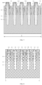
FIG. 3 is a schematic structural diagram of a substrate according to an embodiment of the present application; -
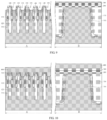
FIG. 4 is a schematic structural diagram of a core region after formation of a first mask layer according to an embodiment of the present application; -
FIG. 5 is a schematic structural diagram of a core region after formation of a first etched hole according to an embodiment of the present application; -
FIG. 6 is a schematic structural diagram of a core region after formation of a bit line contact hole according to an embodiment of the present application; -
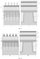
FIG. 7 is a schematic structural diagram of a core region after removal of part of a first conductive layer and part of a first mask layer according to an embodiment of the present application; -
FIG. 8 is a schematic structural diagram of a core region after formation of a bit line contact according to an embodiment of the present application; -
FIG. 9 is a schematic structural diagram after removal of part of a first conductive layer and part of a first mask layer according to an embodiment of the present application; -
FIG. 10 is a schematic structural diagram after formation of a second conductive layer according to an embodiment of the present application; -
FIG. 11 is a schematic structural diagram after removal of part of a second conductive layer according to an embodiment of the present application; -
FIG. 12 is a schematic structural diagram after removal of the remaining first mask layer according to an embodiment of the present application; -
FIG. 13 is a flowchart of after formation of a first mask layer according to an embodiment of the present application; -
FIG. 14 is a schematic structural diagram after formation of a first photoresist layer according to an embodiment of the present application; -
FIG. 15 is a schematic structural diagram after removal of part of an intermediate layer in a core region according to an embodiment of the present application; -
FIG. 16 is a schematic structural diagram after etching of a first anti-reflection layer in a core region according to an embodiment of the present application; -
FIG 17 is a schematic structural diagram after etching of a first base layer in a core region according to an embodiment of the present application; -
FIG 18 is a schematic structural diagram after etching of a second anti-reflection layer in a core region according to an embodiment of the present application; -
FIG. 19 is a schematic structural diagram after etching of a second base layer in a core region according to an embodiment of the present application; -
FIG. 20 is a schematic structural diagram after formation of a first etched hole according to an embodiment of the present application; -
FIG. 21 is a schematic structural diagram after removal of the remaining intermediate layer in a core region according to an embodiment of the present application; -
FIG. 22 is a schematic structural diagram after removal of the remaining second base layer in a core region according to an embodiment of the present application; and -
FIG. 23 is a schematic structural diagram after removal of a second anti-reflection layer in a peripheral region according to an embodiment of the present application. - The inventor of the present application found in actual work that, referring to
FIG. 1 , during deposition of a secondconductive layer 400, abit line contact 410 is formed in the secondconductive layer 400 located in a bit line contact hole, and a void or a seam easily occurs in thebit line contact 410. As shown by dotted lines inFIG. 1 , the void or the seam affects performance of thebit line contact 410, resulting in performance degradation of a memory. - In view of the foregoing technical problem, an embodiment of the present application provides a manufacturing method of a memory. A first mask layer and a first conductive layer around a bit line contact hole in a core region are removed, such that a total depth of a first etched hole and the bit line contact hole is reduced, thereby reducing a formation height of a bit line contact, reducing or even avoiding formation of a void or a seam in the bit line contact, improving a capability of the bit line contact to transmit a charge, and improving performance of the memory.
- In order to make the objectives, features and advantages of the embodiments of the present application clearer, the technical solutions in the embodiments of the present application are described clearly and completely below with reference to the accompanying drawings in the embodiments of the present application. Apparently, the described embodiments are some rather than all of the embodiments of the present application. All other embodiments obtained by a person of ordinary skill in the art based on the embodiments of present application without creative efforts should fall within the protection scope of this application.
-
FIG. 2 shows a procedure of a manufacturing method of a memory according to an embodiment of the present application. The manufacturing method includes the following steps:
Step S101. Provide a substrate, where the substrate includes a core region and a peripheral region located outside the core region, a plurality of active regions are arranged at intervals in the core region, and a first barrier layer is further provided in the core region. - Referring to
FIG. 3 , the substrate includes a core region and a peripheral region, a memory cell (for example, a capacitor) array is formed in the core region to store data information; and a peripheral logic circuit is formed in the peripheral region to control writing or reading of data information. - The peripheral region is provided outside the core region. For example, the peripheral region is provided at a circumferential edge of the core region, that is, the peripheral region is provided around the core region. The core region is shown by A in
FIG. 3 , the peripheral region is shown by B inFIG. 3 , and the peripheral region and the core region may be adjacent to each other. - As shown in
FIG. 3 , a plurality of active regions are arranged at intervals in thecore region 110, and a shallow trench isolation (STI)structure 120 is provided betweenactive regions 110. The shallowtrench isolation structure 120 is filled with an insulating material, such as silicon oxide or silicon oxynitride, so as to isolate theactive regions 110 from each other. A buried word line (BWL) 130 may be further provided in the core region. - The peripheral region may also be provided with
active regions 110. As shown inFIG. 3 , a spacing between theactive regions 110 located in the core region is relatively small, and a spacing between theactive regions 110 located in the peripheral region is relatively large. That is, theactive regions 110 in the core region are denser, and theactive regions 110 located in the peripheral region are sparser. - Still referring to
FIG. 3 , afirst barrier layer 140 is further provided in the core region, and thefirst barrier layer 140 further insulates and protects the core region. A material of thefirst barrier layer 140 may be silicon nitride. For example, thefirst barrier layer 140 is deposited and formed in the core region. As shown inFIG. 3 , thefirst barrier layer 140 is not provided in the peripheral region. - Step S102. Laminate and form a first conductive layer and a first mask layer on the substrate in sequence.
- Referring to
FIG. 4 , a firstconductive layer 200 is formed on the substrate, where the firstconductive layer 200 covers the core region and the peripheral region, and then afirst mask layer 300 is formed on the firstconductive layer 200, where thefirst mask layer 300 covers the firstconductive layer 200. As shown inFIG. 4 , the firstconductive layer 200 and thefirst mask layer 300 are laminated. A material of the firstconductive layer 200 may be polycrystalline silicon, and a material of thefirst mask layer 300 may be oxide, such as silicon oxide. A thickness of thefirst mask layer 300 is greater than or equal to 10 nm. Compared with the related art in which the thickness of thefirst mask layer 300 is usually 50 nm, in this embodiment of the present application, the thickness of thefirst mask layer 300 may be reduced, such that thefirst mask layer 300 is easy to remove subsequently while protecting the firstconductive layer 200. - The first
conductive layer 200 and thefirst mask layer 300 may be formed through a deposition process. For example, the firstconductive layer 200 and thefirst mask layer 300 are formed through chemical vapor deposition (CVD), physical vapor deposition (PVD), or atomic layer deposition (ALD). - Step S103. Etch the first mask layer, the first conductive layer, and the first barrier layer in the core region, to form a first etched hole penetrating through the first mask layer, the first conductive layer, and the first barrier layer, where the first etched hole is opposite to the active region.
- Referring to
FIG. 5 , part of thefirst mask layer 300, part of the firstconductive layer 200, and part of thefirst barrier layer 140 in the core region are removed, to form a firstetched hole 310, where the firstetched hole 310 runs through thefirst mask layer 300, the firstconductive layer 200, and thefirst barrier layer 140. - As shown in
FIG. 5 , the firstetched hole 310 is opposite to theactive region 110. For example, an orthographic projection of the firstetched hole 310 on theactive region 110 covers part of a surface of theactive region 110, for example, covers a central region of an upper surface of theactive region 110. - Step S104. Etch the substrate along the first etched hole, to form a bit line contact hole, where the bit line contact hole exposes the active region.
- Referring to
FIG. 6 , the substrate is etched along the firstetched hole 310, to form a bitline contact hole 150 in the core region. The bitline contact hole 150 exposes theactive region 110, that is, at least part of a hole bottom of the bitline contact hole 150 is theactive region 110. - Step S105. Remove the first mask layer and the first conductive layer in the core region and located around the bit line contact hole, and retain the first barrier layer located around the bit line contact hole.
- Referring to
FIG. 7 , thefirst mask layer 300 and the firstconductive layer 200 in the core region are removed, and thefirst barrier layer 140 in the core region is retained. As shown inFIG. 7 , thefirst barrier layer 140 is exposed in the core region, and after thefirst mask layer 300 and the firstconductive layer 200 in the core region are removed, a thickness of a film layer on the substrate is reduced, that is, a depth of the firstetched hole 310 is reduced, such that a total depth of the firstetched hole 310 and the bitline contact hole 150 is reduced, thereby facilitating subsequent formation of a better-qualitybit line contact 410. - Step S106. Form a bit line contact in the bit line contact hole, where the bit line contact is electrically connected to the active region, and a surface of the bit line contact away from the substrate is flush with a surface of the first barrier layer away from the substrate.
- Referring to
FIG. 8 , abit line contact 410 is formed in the bitline contact hole 150, and thebit line contact 410 is in contact with theactive region 110, such that thebit line contact 410 is electrically connected to theactive region 110. The surface of thebit line contact 410 away from the substrate is flush with a surface of thefirst barrier layer 140 away from the substrate. As shown inFIG. 8 , an upper surface of thebit line contact 410 is flush with an upper surface of thefirst barrier layer 140, such that other relatively flat film layers are formed on thebit line contact 410 and on thefirst barrier layer 140. - Before the formation of the
bit line contact 410, thefirst mask layer 300 and the firstconductive layer 200 located around the bitline contact hole 150 in the core region are removed, such that a formation height of thebit line contact 410 is reduced and formation quality of thebit line contact 410 is good, thereby reducing generation of a void and/or a seam due to uneven filling of thebit line contact 410, improving a capability of thebit line contact 410 to transmit a charge, and improving performance of the memory. - In a possible embodiment, referring to
FIG. 9 to FIG. 11 , the step of forming abit line contact 410 in the bitline contact hole 150 includes:
referring toFIG. 9 and FIG. 10 , depositing a secondconductive layer 400 in the bitline contact hole 150, on thefirst barrier layer 140 in the core region, and on thefirst mask layer 300 in the peripheral region. As shown inFIG. 9 and FIG. 10 , the secondconductive layer 400 fills the bitline contact hole 150, and covers thefirst barrier layer 140 in the core region and thefirst mask layer 300 in the peripheral region. - It can be understood that, the second
conductive layer 400 also fills the remaining firstetched hole 310, that is, the secondconductive layer 400 fills the firstetched hole 310 between the first barrier layers 140. A material of the secondconductive layer 400 may be polycrystalline silicon, such as doped polysilicon or non-doped polysilicon. Certainly, the material of the secondconductive layer 400 is not limited. For example, the material of the secondconductive layer 400 may alternatively be a metal conductive material. - Referring to
FIG. 11 , after the deposition of the secondconductive layer 400, the secondconductive layer 400 on thefirst barrier layer 140 in the core region and the secondconductive layer 400 in the peripheral region are etched and removed. For example, thefirst barrier layer 140 in the core region is used as an etching stop layer, part of the secondconductive layer 400 is etched and removed, and the secondconductive layer 400 located in the bitline contact hole 150 is retained, and the retained secondconductive layer 400 is flush with thefirst barrier layer 140. - The second
conductive layer 400 is etched back after the deposition of the secondconductive layer 400, to form thebit line contact 410. As shown inFIG. 11 , thefirst barrier layer 140 is exposed in the core region, and the firstconductive layer 200 is exposed in the peripheral region. - During the deposition of the second
conductive layer 400, a thickness of a film layer on the substrate is reduced, and a depth of a hole to be filled by the secondconductive layer 400 is reduced, such that deposition difficulty of the secondconductive layer 400 in the bitline contact hole 150 is reduced, and deposition quality is good, thereby reducing or even avoiding formation of a void or a seam in the secondconductive layer 400 in the bitline contact hole 150, that is, reducing or even avoiding occurrence of a void or a seam in thebit line contact 410, and improving formation quality of thebit line contact 410. - Referring to
FIG. 12 , after the secondconductive layer 400 on thefirst barrier layer 140 in the core region and the secondconductive layer 400 in the peripheral region are etched and removed, thefirst mask layer 300 in the peripheral region is etched and removed, to expose the firstconductive layer 200 in the peripheral region. For example, thefirst mask layer 300 in the peripheral region is removed through wet etching. As shown inFIG. 12 , thebit line contact 410 is formed in the core region, and the firstconductive layer 200 is exposed in the peripheral region. - The manufacturing method of a memory in this embodiment of the present application includes: providing a substrate, where the substrate includes a core region and a peripheral region located outside the core region, a plurality of active regions 110 are arranged at intervals in the core region, and a first barrier layer 140 is further provided in the core region; laminating and forming a first conductive layer 200 and a first mask layer 300 on the substrate in sequence; etching the first mask layer 300, the first conductive layer 200, and the first barrier layer 140 in the core region, to form a first etched hole 310, where the first etched hole 310 is opposite to the active region 110; etching the substrate along the first etched hole 310, to form a bit line contact hole 150, where the bit line contact hole 150 exposes the active region 110; removing the first mask layer 300 and the first conductive layer 200 in the core region and located around the bit line contact hole 150, and retaining the first barrier layer 140 located around the bit line contact hole 150; and forming a bit line contact 410 in the bit line contact hole 150, where the bit line contact 410 is electrically connected to the active region 110, and a surface of the bit line contact 410 away from the substrate is flush with a surface of the first barrier layer 140 away from the substrate. The removal of the
first mask layer 300 and the firstconductive layer 200 around the bitline contact hole 150 in the core region reduces a total depth of the firstetched hole 310 and the bitline contact hole 150, such that during subsequent formation of thebit line contact 410, the surface of thebit line contact 410 away from the substrate is flush with the surface of thefirst barrier layer 140 away from the substrate. Compared with the related art in which thebit line contact 410 is flush with the firstconductive layer 200, in the manufacturing method of a memory in this embodiment of the present application, a formation height of thebit line contact 410 is reduced, thereby reducing or even avoiding formation of a void or a seam in thebit line contact 410, that is, improving formation quality of thebit line contact 410, improving a capability of thebit line contact 410 to transmit a charge, and improving performance of the memory. - Referring to
FIG. 13 , in some possible embodiments, after the step of laminating and forming a firstconductive layer 200 and afirst mask layer 300 on the substrate in sequence, the manufacturing method of a memory further includes:
Step S201. Laminate and form a second mask layer, a third mask layer, and an intermediate layer on the first mask layer in sequence, where the third mask layer in the core region has a filling hole penetrating through the third mask layer, and part of the intermediate layer is located in the filling hole. - Referring to
FIG. 14 , asecond mask layer 500 is formed on thefirst mask layer 300, athird mask layer 600 is formed on thesecond mask layer 500, and anintermediate layer 700 is formed on thethird mask layer 600. As shown inFIG. 14 , thefirst mask layer 300, thesecond mask layer 500, thethird mask layer 600, and theintermediate layer 700 form a stacked structure, and all the four film layers are located on the core region and the peripheral region. - As shown in
FIG. 14 , thethird mask layer 600 in the core region has a filling hole, and the filling hole runs through thethird mask layer 600, that is, a hole bottom of the filling hole is thesecond mask layer 500. The filling hole is opposite to theactive region 110. For example, an orthographic projection of the filling hole on theactive region 110 covers part of a surface of theactive region 110 facing away from the substrate. - Part of the
intermediate layer 700 is located in the filling hole, and part of theintermediate layer 700 is located on thethird mask layer 600, that is, part of theintermediate layer 700 is located in thethird mask layer 600, and part of theintermediate layer 700 is located outside thethird mask layer 600. Theintermediate layer 700 located in the filling hole is subsequently used as a mask for the bitline contact hole 150. A material of theintermediate layer 700 may be oxide. - For example, the step of laminating and forming a
second mask layer 500, athird mask layer 600, and anintermediate layer 700 on thefirst mask layer 300 in sequence may include: depositing thesecond mask layer 500 and thethird mask layer 600 on thefirst mask layer 300 in sequence, that is, depositing thesecond mask layer 500 on thefirst mask layer 300, and depositing thethird mask layer 600 on thesecond mask layer 500; etching and removing part of thethird mask layer 600 in the core region, to form the filling hole; and depositing theintermediate layer 700 in the filling hole and on thethird mask layer 600. - It should be noted that, a deposition thickness of the
intermediate layer 700 is greater than a thickness of thethird mask layer 600 and may be less than a preset value, that is, a total height of theintermediate layer 700 along a direction facing away from the substrate is less than a preset value, and theintermediate layer 700 may be removed at the same time with etching of a film layer below theintermediate layer 700 when theintermediate layer 700 is used as a mask. - Step S202. Remove part of the intermediate layer in the core region and the third mask layer in the core region, and retain the intermediate layer located in the filling hole.
- Referring to
FIG. 14 to FIG. 17 , theintermediate layer 700 located in the filling hole is retained, the remainingintermediate layer 700 in the core region is etched and removed, and thethird mask layer 600 in the core region is etched and removed. As shown inFIG. 17 , thesecond mask layer 500 is exposed betweenintermediate layers 700 retained in the core region, and theintermediate layer 700 is exposed in the peripheral region. - In some possible embodiments, the removing the
third mask layer 600 in the core region and part of theintermediate layer 700 in the core region, and retaining theintermediate layer 700 located in the filling hole may include:
referring toFIG. 14 , depositing aphotoresist layer 800 on theintermediate layer 700 in the peripheral region, where thephotoresist layer 800 covers theintermediate layer 700. As shown inFIG. 14 , thephotoresist layer 800 covers theintermediate layer 700 in the peripheral region, and thephotoresist layer 800 does not cover theintermediate layer 700 in the core region, that is, theintermediate layer 700 in the core region is exposed. - Referring to
FIG. 15 , after the deposition of thephotoresist layer 800, theintermediate layer 700 on thethird mask layer 600 in the core region is etched and removed by taking thephotoresist layer 800 as a mask. As shown inFIG. 15 , thethird mask layer 600 is used as an etching stop layer, theintermediate layer 700 is etched, theintermediate layer 700 covered by thephotoresist layer 800 is retained, and theintermediate layer 700 not covered by thephotoresist layer 800 and located on thethird mask layer 600 is removed. - Referring to
FIG. 16 andFIG. 17 , after theintermediate layer 700 on thethird mask layer 600 in the core region is etched and removed, thethird mask layer 600 in the core region and thephotoresist layer 800 in the peripheral region are etched and removed, thesecond mask layer 500 is exposed in the core region, and theintermediate layer 700 is exposed in the peripheral region. - For example, as shown in
FIG. 15 , thethird mask layer 600 includes afirst base layer 610 located on thesecond mask layer 500, and afirst anti-reflection layer 620 located on thefirst base layer 610. A material of thefirst anti-reflection layer 620 may be silicon oxynitride. A material of thefirst base layer 610 may be spin-on carbon (SOC). The step of etching and removing thethird mask layer 600 in the core region and thephotoresist layer 800 in the peripheral region, to expose thesecond mask layer 500 in the core region and theintermediate layer 700 in the peripheral region includes:
etching and removing thefirst anti-reflection layer 620 in the core region, to expose thefirst base layer 610 in the core region. As shown inFIG. 16 , thefirst base layer 610 is used as an etching stop layer, thefirst anti-reflection layer 620 is etched, to remove thefirst anti-reflection layer 620 in the core region, and none of theintermediate layer 700 in the peripheral region and thefirst anti-reflection layer 620 are etched. During the etching and removal of thefirst anti-reflection layer 620 in the core region, theintermediate layer 700 on thefirst base layer 610 in the core region is also removed, that is, thefirst base layer 610 in the core region is flush with theintermediate layer 700 in the core region. - The
first base layer 610 in the core region and thephotoresist layer 800 in the peripheral region are etched and removed at the same time. As shown inFIG. 17 , thefirst base layer 610 in the core region and thephotoresist layer 800 in the peripheral region are removed in a same etching process. - For example, an etch selectivity ratio of the
first base layer 610 to theintermediate layer 700 is greater than or equal to 50, a first etchant is oxygen (O2), a first etching frequency is 60 MHz, and a first etching power is 1000 W to 1200 W. With such settings, thephotoresist layer 800 in the peripheral region is further etched and removed while thefirst base layer 610 is etched and removed, and theintermediate layer 700 in the core region and theintermediate layer 700 in the peripheral region are not removed. - Referring to
FIG. 17 , theintermediate layer 700 is retained in the core region, and theintermediate layer 700 is retained in the peripheral region, such that in a subsequent etching process, theintermediate layer 700 in the core region and theintermediate layer 700 in the peripheral region can be removed at the same time. In addition, film layers in the core region and in the peripheral region have a good correspondence, such that the core region and the peripheral region can be etched at the same time, thereby improving manufacturing efficiency of the memory. For example, thesecond mask layer 500 in the core region and thethird mask layer 600 in the peripheral region can be processed at the same time. - Step S203. Etch and remove, by taking the retained intermediate layer as a mask, the second mask layer exposed in the core region.
- A pattern of the
intermediate layer 700 in the core region is transferred to thesecond mask layer 500, and the etchedsecond mask layer 500 can continue to transfer the pattern to thefirst mask layer 300, the firstconductive layer 200, and thefirst barrier layer 140, to facilitate subsequent formation of the firstetched hole 310 in thefirst mask layer 300, the firstconductive layer 200, and thefirst barrier layer 140. - In the foregoing step, an etch selectivity ratio of the
second mask layer 500 to theintermediate layer 700 is adjusted, such that theintermediate layer 700 in the peripheral region is removed while thesecond mask layer 500 exposed in the core region is removed. It can be understood that, theintermediate layer 700 in the core region is also partially removed. - In some possible embodiments, referring to
FIG. 18 to FIG. 21 , thesecond mask layer 500 includes asecond base layer 510 located on thefirst mask layer 300, and asecond anti-reflection layer 520 located on thesecond base layer 510. - For example, a material of the
second base layer 510 is SOC, and a material of thesecond anti-reflection layer 520 is silicon oxynitride. Correspondingly, the etching and removing, by taking the retainedintermediate layer 700 as a mask, thesecond mask layer 500 exposed in the core region may specifically include:
referring toFIG. 18 , etching and removing thesecond anti-reflection layer 520 exposed in the core region, and etching and removing part of theintermediate layer 700 in the core region and the entireintermediate layer 700 in the peripheral region. As shown inFIG. 18 , thesecond base layer 510 is exposed in the core region, and thethird mask layer 600 is exposed in the peripheral region. - An etch selectivity ratio of the
intermediate layer 700 to thesecond anti-reflection layer 520 is 1, and a thickness of theintermediate layer 700 in the peripheral region is greater than a thickness of thesecond anti-reflection layer 520 and less than 1.2 to 1.3 times a thickness of thesecond anti-reflection layer 520, that is, a thickness of the part of theintermediate layer 700 located on thethird mask layer 600 is greater than a thickness of thesecond anti-reflection layer 520 and less than 1.2 to 1.3 times a thickness of thesecond anti-reflection layer 520, such that theintermediate layer 700 is etched while thesecond anti-reflection layer 520 is etched. - During the etching, a second etchant includes sulfur hexafluoride (SF6) and difluoromethane (CH2F2), and a diluent is nitrogen (N2) or helium (He). Certainly, the second etchant is not limited, and the second etchant may alternatively be other organic compounds or mixtures containing fluorocarbons.
- Referring to
FIG. 19 , thesecond base layer 510 is etched by taking the remainingintermediate layer 700 as a mask, to remove the exposedsecond base layer 510. As shown inFIG. 19 , thefirst mask layer 300 is exposed in the core region, and thethird mask layer 600 is exposed in the peripheral region. - For example, as shown in
FIG. 19 , thethird mask layer 600 includes afirst base layer 610 and afirst anti-reflection layer 620, where thefirst base layer 610 is located on thesecond mask layer 500, and thefirst anti-reflection layer 620 is located on thefirst base layer 610. This embodiment and the following embodiments are described in detail by using an example in which thesecond mask layer 500 includes asecond base layer 510 and asecond anti-reflection layer 520, and thethird mask layer 600 includes afirst base layer 610 and afirst anti-reflection layer 620. - A thickness of the
second base layer 510 is greater than or equal to 1.3 to 1.5 times a thickness of thefirst base layer 610. An etch selectivity ratio of thesecond base layer 510 to thefirst anti-reflection layer 620 is greater than or equal to 20. A fourth etchant may be a mixture of sulfur dioxide (SO2) and oxygen, to etch thesecond base layer 510 while retaining at least part of thefirst anti-reflection layer 620 in the peripheral region. - It can be understood that, the entire
intermediate layer 700 can be removed while thesecond anti-reflection layer 520 exposed in the core region is etched and removed, that is, the entireintermediate layer 700 in the core region and the entireintermediate layer 700 in the peripheral region are etched and removed. Correspondingly, a film layer below theintermediate layer 700 in the core region is used as a mask to transfer a pattern during subsequent etching. For example, thesecond anti-reflection layer 520 is used as a mask during the etching of thesecond base layer 510. - It should be noted that, referring to
FIG. 19 and FIG. 20 , the step of removing thefirst mask layer 300 and the firstconductive layer 200 in the core region and located around the bitline contact hole 150, and retaining thefirst barrier layer 140 located around the bitline contact hole 150 includes: etching thefirst mask layer 300, the firstconductive layer 200, and thefirst barrier layer 140 by taking the remainingintermediate layer 700 as a mask, to form the firstetched hole 310. - As shown in
FIG. 19 and FIG. 20 , after thesecond base layer 510 is etched by taking the remaining intermediate layer 700 a mask, to remove the exposedsecond base layer 510, the remainingintermediate layer 700 is used as a mask to continue to etch thefirst mask layer 300, the firstconductive layer 200, and thefirst barrier layer 140, to form the firstetched hole 310 in the core region. - It should be noted that, referring to
FIG. 21 to FIG. 23 , after the step of etching thesecond base layer 510 by taking the remainingintermediate layer 700 as a mask, to remove the exposedsecond base layer 510, the manufacturing method of a memory further includes:
referring toFIG. 21 , removing the remainingintermediate layer 700, the remainingsecond anti-reflection layer 520 in the core region, and thefirst anti-reflection layer 620 in the peripheral region. As shown inFIG. 21 , thesecond base layer 510 is exposed in the core region, and thefirst base layer 610 is exposed in the peripheral region, such that thefirst base layer 610 and thesecond base layer 510 can be subsequently removed at the same time. - Referring to
FIG. 22 , the remainingsecond base layer 510 in the core region and thefirst base layer 610 in the peripheral region are removed at the same time. For example, an etch selectivity ratio of thefirst base layer 610 to thefirst mask layer 300 is greater than or equal to 50, and an etch selectivity ratio of thefirst base layer 610 to thesecond anti-reflection layer 520 is greater than or equal to 50. A third etchant is oxygen, a second etching frequency is 60 MHz, and a second etching power is 1000 W to 1200 W. As shown inFIG. 22 , thefirst mask layer 300 is exposed in the core region, and thesecond anti-reflection layer 520 is exposed in the peripheral region. - It should be noted that, referring to
FIG. 23 , the step of removing thefirst mask layer 300 and the firstconductive layer 200 in the core region and located around the bitline contact hole 150, and retaining thefirst barrier layer 140 located around the bitline contact hole 150 further includes: removing the remainingfirst mask layer 300 and the remaining firstconductive layer 200 in the core region, and removing thesecond anti-reflection layer 520 in the peripheral region; and removing thesecond base layer 510 in the peripheral region, to expose thefirst mask layer 300 in the peripheral region. - As shown in
FIG. 23 , both the remainingfirst mask layer 300 in the core region and the remaining firstconductive layer 200 in the core region are removed, and thefirst barrier layer 140 is exposed in the core region. Thesecond anti-reflection layer 520 in the peripheral region is also removed, and thesecond base layer 510 is exposed in the peripheral region. - The
first mask layer 300 in the core region, the firstconductive layer 200 in the core region, and thesecond anti-reflection layer 520 in the peripheral region may be removed in this step. For example, thefirst mask layer 300 in the core region, the firstconductive layer 200 in the core region, and thesecond anti-reflection layer 520 in the peripheral region are etched and removed while the substrate is etched along the firstetched hole 310 to form the bitline contact hole 150. Subsequently, thesecond base layer 510 in the peripheral region is removed through wet etching. - The embodiments or implementations of this specification are described in a progressive manner, and each embodiment focuses on differences from other embodiments. The same or similar parts between the embodiments may refer to each other.
- In the descriptions of this specification, a description with reference to the term "one implementation", "some implementations", "an exemplary implementation", "an example", "a specific example", "some examples", or the like means that a specific feature, structure, material, or characteristic described in combination with the implementation(s) or example(s) is included in at least one implementation or example of the present disclosure. In this specification, the schematic expression of the above terms does not necessarily refer to the same implementation or example. Moreover, the described specific feature, structure, material or characteristic may be combined in an appropriate manner in any one or more implementations or examples.
- Finally, it should be noted that the above embodiments are merely used to explain the technical solutions of the present application, but are not intended to limit the present application. Although the present application is described in detail with reference to the foregoing embodiments, those of ordinary skill in the art should understand that they can still modify the technical solutions described in the foregoing embodiments, or make equivalent substitutions on some or all technical features therein. These modifications or substitutions do not make the essence of the corresponding technical solutions deviate from the spirit and scope of the technical solutions of the embodiments of the present application.
Claims (15)
- A manufacturing method of a memory, comprising:providing a substrate; wherein the substrate comprises a core region and a peripheral region located outside the core region, a plurality of active regions are arranged at intervals in the core region, and a first barrier layer is further provided in the core region;laminating and forming a first conductive layer and a first mask layer on the substrate in sequence;etching the first mask layer, the first conductive layer, and the first barrier layer which are in the core region, to form a first etched hole penetrating through the first mask layer, the first conductive layer, and the first barrier layer; wherein the first etched hole is opposite to the active region;etching the substrate along the first etched hole, to form a bit line contact hole; wherein the bit line contact hole exposes the active region;removing the first mask layer and the first conductive layer which are in the core region and located around the bit line contact hole, and retaining the first barrier layer located around the bit line contact hole; andforming a bit line contact in the bit line contact hole; wherein the bit line contact is electrically connected to the active region, and a surface of the bit line contact away from the substrate is flush with a surface of the first barrier layer away from the substrate.
- The manufacturing method of a memory according to claim 1, wherein after the step of laminating and forming a first conductive layer and a first mask layer on the substrate in sequence, the manufacturing method of a memory further comprises:laminating and forming a second mask layer, a third mask layer, and an intermediate layer on the first mask layer in sequence; wherein the third mask layer in the core region has a filling hole penetrating through the third mask layer, and part of the intermediate layer is located in the filling hole;removing part of the intermediate layer in the core region and the third mask layer in the core region, and retaining the intermediate layer located in the filling hole; andetching and removing, by taking a retained intermediate layer as a mask, the second mask layer exposed in the core region.
- The manufacturing method of a memory according to claim 2, wherein the step of removing part of the intermediate layer in the core region and the third mask layer in the core region, and retaining the intermediate layer located in the filling hole comprises:depositing a photoresist layer on the intermediate layer in the peripheral region, wherein the photoresist layer covers the intermediate layer;etching and removing, by taking the photoresist layer as a mask, the intermediate layer on the third mask layer in the core region; andetching and removing the third mask layer in the core region and the photoresist layer in the peripheral region, to expose the second mask layer in the core region and the intermediate layer in the peripheral region.
- The manufacturing method of a memory according to claim 3, wherein the third mask layer comprises a first base layer located on the second mask layer, and a first anti-reflection layer located on the first base layer; and
the step of etching and removing the third mask layer in the core region and the photoresist layer in the peripheral region, to expose the second mask layer in the core region and the intermediate layer in the peripheral region, comprises:etching and removing the first anti-reflection layer in the core region, to expose the first base layer in the core region; andetching and removing the first base layer in the core region and the photoresist layer in the peripheral region at the same time. - The manufacturing method of a memory according to claim 4, wherein an etch selectivity ratio of the first base layer to the intermediate layer is greater than or equal to 50; and
when the first base layer in the core region and the photoresist layer in the peripheral region are etched and removed at the same time, a first etchant is oxygen, a first etching frequency is 60 MHz, and a first etching power is 1000 W to 1200 W. - The manufacturing method of a memory according to claim 2, wherein the step of laminating and forming a second mask layer, a third mask layer, and an intermediate layer on the first mask layer in sequence comprises:depositing the second mask layer and the third mask layer on the first mask layer in sequence;etching and removing part of the third mask layer in the core region, to form the filling hole; anddepositing the intermediate layer in the filling hole and on the third mask layer.
- The manufacturing method of a memory according to claim 2, wherein the second mask layer comprises a second base layer located on the first mask layer, and a second anti-reflection layer located on the second base layer; and
the step of etching and removing, by taking a retained intermediate layer as a mask, the second mask layer exposed in the core region comprises:etching and removing the second anti-reflection layer exposed in the core region, and etching and removing part of the intermediate layer in the core region and an entire intermediate layer in the peripheral region; andetching the second base layer by taking a remaining intermediate layer as a mask, to remove an exposed second base layer. - The manufacturing method of a memory according to claim 7, wherein an etch selectivity ratio of the intermediate layer to the second anti-reflection layer is 1, and a thickness of the intermediate layer is less than 1.2 to 1.3 times a thickness of the second anti-reflection layer, such that the intermediate layer is etched while the second anti-reflection layer is etched.
- The manufacturing method of a memory according to claim 7, wherein when the second anti-reflection layer exposed in the core region is etched and removed, and part of the intermediate layer in the core region and the entire intermediate layer in the peripheral region are etched and removed, a second etchant comprises sulfur hexafluoride and difluoromethane, and a diluent is nitrogen or helium.
- The manufacturing method of a memory according to claim 7, wherein the third mask layer comprises a first base layer located on the second mask layer, and a first anti-reflection layer located on the first base layer;a thickness of the second base layer is greater than or equal to 1.3 to 1.5 times a thickness of the first base layer; andan etch selectivity ratio of the second base layer to the first anti-reflection layer is greater than or equal to 20, such that at least part of the first anti-reflection layer in the peripheral region is retained while the second base layer is etched.
- The manufacturing method of a memory according to claim 7, wherein the third mask layer comprises a first base layer located on the second mask layer, and a first anti-reflection layer located on the first base layer; and
after the step of etching the second base layer by taking a remaining intermediate layer as a mask, to remove an exposed second base layer, the manufacturing method of a memory further comprises:removing the remaining intermediate layer, a remaining second anti-reflection layer in the core region, and the first anti-reflection layer in the peripheral region; andremoving a remaining second base layer in the core region and the first base layer in the peripheral region at the same time. - The manufacturing method of a memory according to claim 11, wherein an etch selectivity ratio of the first base layer to the first mask layer is greater than or equal to 50, and an etch selectivity ratio of the first base layer to the second anti-reflection layer is greater than or equal to 50; and
when the remaining second base layer in the core region and the first base layer in the peripheral region are removed at the same time, a third etchant is oxygen, a second etching frequency is 60 MHz, and a second etching power is 1000 W to 1200 W. - The manufacturing method of a memory according to claim 7, wherein the step of etching the first mask layer, the first conductive layer, and the first barrier layer which are in the core region, to form a first etched hole penetrating through the first mask layer, the first conductive layer, and the first barrier layer, wherein the first etched hole is opposite to the active region comprises:
etching the first mask layer, the first conductive layer, and the first barrier layer by taking the remaining intermediate layer as a mask, to form the first etched hole. - The manufacturing method of a memory according to claim 13, wherein the step of removing the first mask layer and the first conductive layer in the core region and located around the bit line contact hole, and retaining the first barrier layer located around the bit line contact hole further comprises:removing a remaining first mask layer and a remaining first conductive layer in the core region, and removing the second anti-reflection layer in the peripheral region; andremoving the second base layer in the peripheral region, to expose the first mask layer in the peripheral region.
- The manufacturing method of a memory according to claim 1, wherein the step of forming a bit line contact in the bit line contact hole comprises:depositing a second conductive layer in the bit line contact hole, on the first barrier layer in the core region, and on the first mask layer in the peripheral region;etching and removing the second conductive layer on the first barrier layer in the core region and the second conductive layer in the peripheral region; andetching and removing the first mask layer in the peripheral region, to expose the first conductive layer in the peripheral region.
Applications Claiming Priority (2)
| Application Number | Priority Date | Filing Date | Title |
|---|---|---|---|
| CN202110527256.8A CN113284852B (en) | 2021-05-14 | 2021-05-14 | Method for manufacturing memory |
| PCT/CN2021/110999 WO2022236980A1 (en) | 2021-05-14 | 2021-08-05 | Method for manufacturing memory |
Publications (3)
| Publication Number | Publication Date |
|---|---|
| EP4220700A1 true EP4220700A1 (en) | 2023-08-02 |
| EP4220700A4 EP4220700A4 (en) | 2024-04-24 |
| EP4220700B1 EP4220700B1 (en) | 2026-05-06 |
Family
ID=83695663
Family Applications (1)
| Application Number | Title | Priority Date | Filing Date |
|---|---|---|---|
| EP21941549.4A Active EP4220700B1 (en) | 2021-05-14 | 2021-08-05 | Manufacturing method of memory |
Country Status (2)
| Country | Link |
|---|---|
| US (1) | US11482526B1 (en) |
| EP (1) | EP4220700B1 (en) |
Family Cites Families (9)
| Publication number | Priority date | Publication date | Assignee | Title |
|---|---|---|---|---|
| KR101979901B1 (en) * | 2012-12-05 | 2019-08-28 | 삼성전자주식회사 | Method for fabricating a semiconductor device |
| KR20150101074A (en) * | 2014-02-26 | 2015-09-03 | 삼성전자주식회사 | Photoresist composition, method of forming a pattern using the same, and method of manufacturing a semiconductor device using the same |
| KR20180129387A (en) * | 2017-05-26 | 2018-12-05 | 에스케이하이닉스 주식회사 | Semiconductor device and method for fabricating the same |
| KR102525163B1 (en) * | 2018-05-15 | 2023-04-24 | 삼성전자주식회사 | Integrated circuit device |
| KR102691653B1 (en) | 2019-06-07 | 2024-08-05 | 삼성전자주식회사 | Semiconductor devices |
| CN112530946B (en) | 2019-09-18 | 2022-12-16 | 长鑫存储技术有限公司 | Semiconductor structure and manufacturing method thereof |
| CN112563208A (en) | 2019-09-26 | 2021-03-26 | 长鑫存储技术有限公司 | Semiconductor memory and method of manufacturing the same |
| CN111640749B (en) | 2019-11-14 | 2025-03-28 | 福建省晋华集成电路有限公司 | Memory and method of forming the same |
| US11309316B1 (en) * | 2020-10-20 | 2022-04-19 | Nanya Technology Corporation | Semiconductor device with single step height and method for fabricating the same |
-
2021
- 2021-08-05 EP EP21941549.4A patent/EP4220700B1/en active Active
- 2021-11-01 US US17/453,038 patent/US11482526B1/en active Active
Also Published As
| Publication number | Publication date |
|---|---|
| US20220367478A1 (en) | 2022-11-17 |
| EP4220700A4 (en) | 2024-04-24 |
| EP4220700B1 (en) | 2026-05-06 |
| US11482526B1 (en) | 2022-10-25 |
Similar Documents
| Publication | Publication Date | Title |
|---|---|---|
| US6716757B2 (en) | Method for forming bottle trenches | |
| US7262090B2 (en) | Random access memory (RAM) capacitor in shallow trench isolation with improved electrical isolation to overlying gate electrodes | |
| US6509599B1 (en) | Trench capacitor with insulation collar and method for producing the trench capacitor | |
| CN112992775B (en) | Semiconductor memory and forming method thereof | |
| CN113284852B (en) | Method for manufacturing memory | |
| US12526981B2 (en) | Semiconductor structure with a high depth-width ratio capacitor and manufacturing method thereof | |
| US11882683B2 (en) | Method of forming semiconductor memory device having saddle portion | |
| US6787838B1 (en) | Trench capacitor DRAM cell using buried oxide as array top oxide | |
| US10535664B2 (en) | Fabricating method of oxide layer within peripheral circuit region | |
| CN113594098B (en) | Semiconductor device and method for manufacturing the same | |
| US11482526B1 (en) | Manufacturing method of memory | |
| US12225718B2 (en) | Semiconductor structure and method for forming semiconductor structure | |
| CN218941671U (en) | Semiconductor device with a semiconductor layer having a plurality of semiconductor layers | |
| CN215299254U (en) | Semiconductor device with a plurality of transistors | |
| CN115000150A (en) | Semiconductor device, electronic apparatus and manufacturing method | |
| KR20110080783A (en) | Method of manufacturing semiconductor device | |
| US12513881B2 (en) | Semiconductor structure and manufacturing method thereof | |
| US12453081B2 (en) | Method of forming a bit line structure | |
| US12342586B2 (en) | Semiconductor structure and manufacturing method thereof | |
| CN117529105B (en) | Semiconductor structure and forming method thereof | |
| US11942522B2 (en) | Method for manufacturing semiconductor structure and semiconductor structure | |
| US20240381625A1 (en) | Methods of manufacturing semiconductor device | |
| CN114446890A (en) | Memory manufacturing method and memory | |
| US20220246617A1 (en) | Method for manufacturing semiconductor structure and semiconductor structure | |
| CN116669418A (en) | Semiconductor device and manufacturing method |
Legal Events
| Date | Code | Title | Description |
|---|---|---|---|
| STAA | Information on the status of an ep patent application or granted ep patent |
Free format text: STATUS: THE INTERNATIONAL PUBLICATION HAS BEEN MADE |
|
| PUAI | Public reference made under article 153(3) epc to a published international application that has entered the european phase |
Free format text: ORIGINAL CODE: 0009012 |
|
| STAA | Information on the status of an ep patent application or granted ep patent |
Free format text: STATUS: REQUEST FOR EXAMINATION WAS MADE |
|
| 17P | Request for examination filed |
Effective date: 20230424 |
|
| AK | Designated contracting states |
Kind code of ref document: A1 Designated state(s): AL AT BE BG CH CY CZ DE DK EE ES FI FR GB GR HR HU IE IS IT LI LT LU LV MC MK MT NL NO PL PT RO RS SE SI SK SM TR |
|
| REG | Reference to a national code |
Ref country code: DE Ref legal event code: R079 Free format text: PREVIOUS MAIN CLASS: H01L0021824200 Ipc: H10B0012000000 Ref document number: 602021054148 Country of ref document: DE |
|
| A4 | Supplementary search report drawn up and despatched |
Effective date: 20240327 |
|
| RIC1 | Information provided on ipc code assigned before grant |
Ipc: H10B 12/00 20230101AFI20240321BHEP |
|
| DAV | Request for validation of the european patent (deleted) | ||
| DAX | Request for extension of the european patent (deleted) | ||
| GRAP | Despatch of communication of intention to grant a patent |
Free format text: ORIGINAL CODE: EPIDOSNIGR1 |
|
| STAA | Information on the status of an ep patent application or granted ep patent |
Free format text: STATUS: GRANT OF PATENT IS INTENDED |
|
| INTG | Intention to grant announced |
Effective date: 20260126 |
|
| GRAS | Grant fee paid |
Free format text: ORIGINAL CODE: EPIDOSNIGR3 |
|
| GRAA | (expected) grant |
Free format text: ORIGINAL CODE: 0009210 |
|
| STAA | Information on the status of an ep patent application or granted ep patent |
Free format text: STATUS: THE PATENT HAS BEEN GRANTED |
|
| P01 | Opt-out of the competence of the unified patent court (upc) registered |
Free format text: CASE NUMBER: UPC_APP_0009783_4220700/2026 Effective date: 20260313 |
|
| AK | Designated contracting states |
Kind code of ref document: B1 Designated state(s): AL AT BE BG CH CY CZ DE DK EE ES FI FR GB GR HR HU IE IS IT LI LT LU LV MC MK MT NL NO PL PT RO RS SE SI SK SM TR |
|
| REG | Reference to a national code |
Ref country code: CH Ref legal event code: F10 Free format text: ST27 STATUS EVENT CODE: U-0-0-F10-F00 (AS PROVIDED BY THE NATIONAL OFFICE) Effective date: 20260506 Ref country code: GB Ref legal event code: FG4D |