EP4220685A1 - Manufacturing method for semiconductor structure, and semiconductor structure - Google Patents
Manufacturing method for semiconductor structure, and semiconductor structure Download PDFInfo
- Publication number
- EP4220685A1 EP4220685A1 EP21950608.6A EP21950608A EP4220685A1 EP 4220685 A1 EP4220685 A1 EP 4220685A1 EP 21950608 A EP21950608 A EP 21950608A EP 4220685 A1 EP4220685 A1 EP 4220685A1
- Authority
- EP
- European Patent Office
- Prior art keywords
- substrate
- transistors
- semiconductor structure
- forming
- initial
- Prior art date
- Legal status (The legal status is an assumption and is not a legal conclusion. Google has not performed a legal analysis and makes no representation as to the accuracy of the status listed.)
- Granted
Links
Images

Classifications
-
- H—ELECTRICITY
- H10—SEMICONDUCTOR DEVICES; ELECTRIC SOLID-STATE DEVICES NOT OTHERWISE PROVIDED FOR
- H10B—ELECTRONIC MEMORY DEVICES
- H10B12/00—Dynamic random access memory [DRAM] devices
- H10B12/01—Manufacture or treatment
- H10B12/02—Manufacture or treatment for one transistor one-capacitor [1T-1C] memory cells
- H10B12/05—Making the transistor
-
- H—ELECTRICITY
- H10—SEMICONDUCTOR DEVICES; ELECTRIC SOLID-STATE DEVICES NOT OTHERWISE PROVIDED FOR
- H10B—ELECTRONIC MEMORY DEVICES
- H10B12/00—Dynamic random access memory [DRAM] devices
- H10B12/30—DRAM devices comprising one-transistor - one-capacitor [1T-1C] memory cells
- H10B12/33—DRAM devices comprising one-transistor - one-capacitor [1T-1C] memory cells the capacitor extending under the transistor
-
- H—ELECTRICITY
- H10—SEMICONDUCTOR DEVICES; ELECTRIC SOLID-STATE DEVICES NOT OTHERWISE PROVIDED FOR
- H10B—ELECTRONIC MEMORY DEVICES
- H10B12/00—Dynamic random access memory [DRAM] devices
- H10B12/30—DRAM devices comprising one-transistor - one-capacitor [1T-1C] memory cells
- H10B12/48—Data lines or contacts therefor
- H10B12/482—Bit lines
-
- H—ELECTRICITY
- H10—SEMICONDUCTOR DEVICES; ELECTRIC SOLID-STATE DEVICES NOT OTHERWISE PROVIDED FOR
- H10D—INORGANIC ELECTRIC SEMICONDUCTOR DEVICES
- H10D1/00—Resistors, capacitors or inductors
- H10D1/60—Capacitors
- H10D1/68—Capacitors having no potential barriers
- H10D1/692—Electrodes
- H10D1/711—Electrodes having non-planar surfaces, e.g. formed by texturisation
- H10D1/716—Electrodes having non-planar surfaces, e.g. formed by texturisation having vertical extensions
Definitions
- DRAMs Dynamic Random Access Memories
- ROMs Read Only Memories
- the present disclosure provides a method for manufacturing a semiconductor structure and a semiconductor structure.
- the first aspect of the present disclosure provides a method for manufacturing a semiconductor structure, including:
- the second aspect of the embodiments of the present disclosure provides a semiconductor structure, comprising:
- a conductive structure is formed in the substrate, one end of the conductive structure is connected to the transistor, and when there are excess holes in the transistor, the holes can be transferred to the outside of the substrate by the conductive structure, thereby avoiding the floating gate effect between the substrate and the transistors and improving the performance of the semiconductor structure.
- a conductive structure is formed in the substrate, one end of the conductive structure is connected to the transistor, and when there are excess holes in the transistor, the holes can be transferred to the outside of the substrate by the conductive structure, thereby avoiding the floating gate effect between the substrate and the transistor and improving the performance of the semiconductor structure.
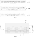
- FIG. 1 shows a flowchart of a method for manufacturing a semiconductor structure according to an exemplary embodiment of the present disclosure
- FIGS. 2 to 10 are schematic diagrams of various stages of the method for manufacturing a semiconductor structure. The method for manufacturing a semiconductor structure will be introduced below in conjunction with FIGS. 2 to 10.
- This embodiment does not limit the semiconductor structure.
- the following will introduce the semiconductor structure by taking a Dynamic Random Access Memory (DRAM) as an example, but this embodiment is not limited to this.
- DRAM Dynamic Random Access Memory
- the semiconductor structure in this embodiment may also be other structure.
- a method for manufacturing a semiconductor structure includes the following steps: Step S100: a substrate is provided, the substrate having a first surface and a second surface opposite to each other, and transistors being arranged on the second surface.
- the substrate 10 is used as a support component of the dynamic random access memory to support other components disposed thereon.
- the substrate 10 may be made of a semiconductor material, and the semiconductor material may be one or more of silicon, germanium, a silicon-germanium compound and a silicon-carbon compound.
- an initial substrate 11 is provided, the initial substrate 11 having a first initial surface 111 and a second surface 102 opposite to each other;
- the surface of the remaining of the initial substrate 11 forms the first surface 101, and the remaining of the initial substrate 11 forms the substrate 10.
- the first initial surface 111 may be planarized using a chemical mechanical polishing process, and remove part of the thickness of the initial substrate 11, the remaining of the initial substrate 11 forms the substrate 10, and the planarized first initial surface 111 forms the first surface 101.
- a transistor 20 is further arranged on the second surface 102.
- an isolation structure 30 may be formed on the second surface through a deposition process, then the isolation structure 30 is patterned to form a plurality of trenches in the isolation structure 30, the trenches are arranged at intervals in a first direction, that is, the X direction shown in FIG. 2 , a bit line structure 50 is formed in each trench, and a plurality of active columns arranged in an array are formed on the bit line structures 50.
- a word line 40 extending in the first direction is formed on the isolation structure 30, part of the word line 40 wraps a channel region 22 of each active column, and each active column and the word line 40 wrapping the active column constitute a transistor 20.
- An air gap layer 31 is further formed in the isolation structure 30.
- Step S200 release holes are formed in the substrate, the release holes extending into the transistors, bottoms of the release holes being located in channel regions of the transistors, and top surfaces of the release holes being flush with the first surface.
- a mask layer 70 is formed on the first surface 101.
- the mask layer 70 may be formed on the first surface 101 by a deposition process.
- the mask layer 70 may be a single film layer or a laminated structure.
- the mask layer may include a first mask layer 71 and a second mask layer 72 laminated, the first mask layer 71 is arranged on a first dielectric layer 60, and the first dielectric layer 60 may include a silicon oxide layer, wherein the material of the first mask layer 71 is different from the material of the second mask layer 72, for example, the material of the first mask layer 71 may include amorphous carbon, and the material of the second mask layer 72 may include silicon oxynitride.
- a photoresist layer 80 may be formed on the mask layer 70 by coating, and then the photoresist layer is patterned by exposure, development, or etching to form a mask pattern in the photoresist layer 80, wherein the mask pattern includes a plurality of first openings 81 and bumps 82 for separating the first openings 81, the number of the first openings 81 corresponds to the number of the transistors 20 one to one, and the projection of the first opening 81 in the transistor 20 is located in a source 21 of the transistor 20.
- an oxide layer 100 is formed on side walls of the first openings 81, the oxide layer 100 extends to the outside of the first openings 81 and cover the top surface of the mask layer 70, and the oxide layer 100 located in the first openings 81 encloses second openings 83, wherein the oxide layer 100 may be a silicon oxide layer.
- an initial oxide layer 110 may be formed on the side walls and bottom walls of the first openings 81 by an atomic layer deposition process, and the initial oxide layer 110 extends to the outside of the first openings 81 and covers the top surface of the mask layer 70.
- the initial oxide layer 110 located on the bottom walls of the second openings 83 is removed with an etching gas or etching solution, and the remaining of the initial oxide layer 110 forms the oxide layer 100, that is, the formed oxide layer 100 covers the top surfaces and side walls of the bumps 82, wherein the oxide layer 100 located in the first openings 81 encloses the second openings 83.
- the mask layer 70, the substrate 10, the sources 21 of the transistors 20 and part of the channel regions 22 of the transistors 20 that are exposed in the second openings 83 are removed with the etching solution or etching gas, to form the release holes 90, as shown in FIG. 6 .
- multiple times of pattern transfer can ensure the accuracy of the pattern finally transferred to the substrate 10 and the transistors 20, and improve the accuracy of the release hole 90.
- the first dielectric layer 60 is arranged on the first surface 101 to protect the substrate 10, which can reduce lateral etching of the substrate 10 when the release holes 90 are formed, to improve the performance of the semiconductor structure.
- Step S300 a conductive structure is formed in the release holes, the conductive structure extending to the outside of the release holes and covering the first surface of the substrate.
- a second initial dielectric layer 131 is formed in the release holes 90 by an atomic layer deposition process, the second initial dielectric layer 131 extending to the outside of the release holes 90 and covering the first dielectric layer 60.
- the second initial dielectric layer 131 on the first dielectric layer 60 and the second initial dielectric layer 131 on the bottom of the release holes 90 are removed with an etching solution or etching gas, the remaining of the second initial dielectric layer 131 forms a second dielectric layer 130, and the second dielectric layer 130 encloses intermediate holes 140 in the release holes 90, as shown in FIG. 8 .
- the conductive structure 150 is formed in the intermediate holes by a deposition process, the conductive structure 150 extending to the outside of the intermediate holes 140 and covering the first dielectric layer 60, wherein the material of the conductive structure 150 may include conductive materials such as copper, aluminum or tungsten.
- the deposition process may include an atomic layer deposition process, a physical vapor deposition process, or a chemical vapor deposition process.
- a conductive structure is formed in the substrate, one end of the conductive structure is connected to the transistors, and when there are excess holes in the transistors, the holes can be transferred to the outside of the substrate by the conductive structure, thereby avoiding the floating gate effect between the substrate and the transistors and improving the performance of the semiconductor structure.
- an embodiment of the present disclosure further provides a semiconductor structure, including:
- the material of the conductive body 151 and the material of the conductive bumps 152 are metal materials, for example, the materials of the conductive body 151 and the conductive bumps 152 may include one of copper, aluminum, or tungsten.
- a conductive structure is formed in the substrate, one end of the conductive structure is connected to the channel regions of the transistors, and when there are excess holes in the transistor, the holes can be transferred to the outside of the substrate by the conductive structure, thereby avoiding the floating gate effect between the substrate and the transistors and improving the performance of the semiconductor structure.
- the semiconductor structure further includes a first dielectric layer 60, the first dielectric layer 60 is arranged between the first surface 101 and the conductive body 151, and the ends of the conductive bumps 152 away from the conductive body 151 penetrate the first dielectric layer 60 and then are communicated with the channel regions 22 of the transistors 20, wherein the material of the first dielectric layer 60 may include silicon oxide.
- the first dielectric layer 60 can avoid electrical connection of the conductive body 151 to other devices arranged in the substrate 10, which ensures normal use of the semiconductor structure.
- the semiconductor structure further includes a second dielectric layer 130, and the second dielectric layer 130 is arranged on the surfaces of the conductive bumps 152, wherein the material of the second dielectric layer 130 may include silicon nitride.
- the second dielectric layer 130 can avoid electrical connection of the conductive bump 152 to a drain 23 of the transistor 20 or other devices arranged in the substrate 10, which ensures the performance of the semiconductor structure.
- the substrate 10 is provided with a plurality of bit line structures 50 arranged in a row direction of the transistors 20, the top surfaces of the bit line structures 50 are located on the second surface 102, and the sources 21 of the transistors 20 are connected to the bit line structures 50.
- the row direction of the transistors 20 may be the X direction shown in the figures.
- the plurality of bit line structures 50 may be arranged at intervals in the row direction of the transistors 20, and the bit line structures 50 may extend in a column direction of the transistors 20, that is, the bit line structures 50 may extend in a direction perpendicular to the X direction.
- the substrate 10 is formed with a plurality of word lines 40 arranged in the column direction of the transistors 20, and the word lines 40 are configured to connect the channel regions 22 of the plurality of transistors 20.
- a third dielectric layer and an isolation layer stacked are formed on the word lines 40, the third dielectric layer abuts against the word lines 40, the third dielectric layer includes a silicon oxide layer, and the isolation layer includes a silicon nitride layer.
- a capacitor contact structure 160 is connected to the drain 23 of one of the transistor 20, and a capacitor structure 170 is connected to the capacitor contact structure 160, wherein the capacitor structure 170 includes an top electrode 171, a dielectric layer 172 and a bottom electrode 173, and a capacitor pad 180 may be connected to the bottom electrode 173.
- capacitor structure 170 and the capacitor contact structure 160 are further provided with a plurality of support layers and third dielectric layers alternately arranged in sequence.
- the capacitor contact structure 160 includes a first contact structure 161 and a second contact structure 162 adhered, the end of the first contact structure 161 away from the second contact structure 162 is connected to the drain 23 of one of the transistor 20, and the end of the second contact structure 162 away from the first contact structure 161 is connected to one of the capacitor structure 170.
- This embodiment realizes the connection between the capacitor structure and the drains of the transistors through the capacitor contact structure.
- a voltage is applied to the word lines to open the channel regions of the transistors, so that the sources of the transistors are connected to the drains.
- the data on the word lines is transmitted to the drains by the sources, and then transmitted to the capacitor structure by the capacitor contact structure for storage.
- the first contact structure 161 may be in a regular shape, for example, a rectangular shape or a cylindrical shape, or in an irregular shape.
- the first contact structure 161 includes a first segment 1611 and a second segment 1612 connected to the first segment 1611, the end of the first segment 1611 away from the second segment 1612 is connected to the drain 23, and the end of the second segment 1612 away from the first segment 1611 is connected to the second contact structure 162.
- the longitudinal section of the first segment 1611 is a rectangle
- the longitudinal section of the second segment 1612 is a trapezoid enlarged from top to bottom, which can increase the area of the first contact structure 161 to reduce the resistance of the first contact structure 161 and improve the sensitivity of signal transmission.
- the second contact structure 162 includes a third segment 1621 and a fourth segment 1622 connected to the third segment 1621, the end of the third segment 1621 away from the fourth segment 1622 is connected to the first contact structure 161, and the end of the fourth segment 1622 away from the third segment 1621 is connected to one end of the capacitor structure 170.
- the longitudinal section of the third segment 1621 is a trapezoid reduced from top to bottom
- the longitudinal section of the fourth segment 1622 is a rectangle, which can enlarge the contact area between the second contact structure 162 and the first contact structure 161 to reduce the contact resistance and improve the sensitivity of signal transmission.
- the first contact structure 161 has a first surface and a second surface opposite to each other, that is, the first surface forms one end of the first segment 1611, and the second segment forms the end of the second segment 1612 away from the first segment 1611.
- the second contact structure 162 has a third surface and a fourth surface opposite to each other, that is, the third surface forms one end of the third segment 1621, and the fourth surface forms the end of the fourth segment 1622 away from the third segment 1621.
- the second surface is connected to the drain 23 of one of the transistor 20, the first surface is connected to the third surface, and the fourth surface is connected to one of the capacitor structure 170.
- the projection area of the first surface on the substrate 10 is larger than the projection area of the third surface on the substrate 10, which facilitates the alignment of the first contact structure 161 and the second contact structure 162.
- a conductive structure is formed in the substrate, one end of the conductive structure is connected to one of the channel region of the transistor, and when there are excess holes in the transistor, the holes can be transferred to the outside of the substrate by the conductive structure, thereby avoiding the floating gate effect between the substrate and the transistor and improving the performance of the semiconductor structure.
- first, second, etc. used in the present disclosure can be used in the present disclosure to describe various structures, but these structures are not limited by these terms. These terms are only configured to distinguish the first structure from another structure.
- a conductive structure is formed in the substrate, one end of the conductive structure is connected to the transistor, and when there are excess holes in the transistor, the holes can be transferred to the outside of the substrate by the conductive structure, thereby avoiding the floating gate effect between the substrate and the transistor and improving the performance of the semiconductor structure.
Landscapes
- Engineering & Computer Science (AREA)
- Manufacturing & Machinery (AREA)
- Internal Circuitry In Semiconductor Integrated Circuit Devices (AREA)
Abstract
Description
- The present disclosure claims the priority to
Chinese Patent Application 202110812549.0, titled "METHOD FOR MANUFACTURING SEMICONDUCTOR STRUCTURE AND SEMICONDUCTOR STRUCTURE", filed on July 19, 2021 - The present disclosure relates to, but is not limited to, a method for manufacturing a semiconductor structure and a semiconductor structure.
- Dynamic Random Access Memories (DRAMs) have the advantages of small size, high integration and low power consumption, and are faster than all Read Only Memories (ROMs). With the increase in integration, the feature size of a capacitor and the area of an electrode plate continue to decrease, so dielectric materials that are thinner or/and have higher dielectric constants have to be used to increase the capacitance density. With the development of the semiconductor industry, the critical dimensions of devices such as DRAMs continue to decrease.
- However, as the critical dimensions of the devices continue to decrease, a floating gate effect will occur between a transistor and a substrate. This is because, when the transistor is in an off state, some charges in the capacitor structure move into the transistor through a capacitor contact structure and a capacitor pad, as a result, holes in the transistor are increased to increase the voltage in the transistor, a voltage difference is produced between the transistor and the substrate, and then the floating gate effect is produced, which will affect the performance of the semiconductor structure.
- The subject matter is described in detail herein below, which is not intended to limit the scope of protection of claims.
- The present disclosure provides a method for manufacturing a semiconductor structure and a semiconductor structure.
- The first aspect of the present disclosure provides a method for manufacturing a semiconductor structure, including:
- providing a substrate, the substrate having a first surface and a second surface opposite to each other, and transistors being arrange don the second surface;
- forming release holes in the substrate, the release holes extending into the transistors, bottoms of the release holes being located in channel regions of the transistors, and top surfaces of the release holes being flush with the first surface; and
- forming a conductive structure in the release holes, the conductive structure extending to the outside of the release holes and covering the first surface of the substrate.
- The second aspect of the embodiments of the present disclosure provides a semiconductor structure, comprising:
- a substrate, the substrate having a first surface and a second surface opposite to each other, a plurality of transistors being arrange don the second surface, and the transistors being arranged in an array; and
- a conductive structure, the conductive structure comprising a conductive body and a plurality of conductive bumps arranged on the conductive body, the conductive body being arranged on the first surface, each of the conductive bumps corresponds to one transistor, and ends of the conductive bumps away from the conductive body passing through the substrate and sources of the transistors and then being communicated with channel regions of the transistors.
- In the method for manufacturing a semiconductor structure and the semiconductor structure provided by the embodiments of the present disclosure, a conductive structure is formed in the substrate, one end of the conductive structure is connected to the transistor, and when there are excess holes in the transistor, the holes can be transferred to the outside of the substrate by the conductive structure, thereby avoiding the floating gate effect between the substrate and the transistors and improving the performance of the semiconductor structure.
- After the drawings and detailed description are read and understood, other aspects may be understood.
- The drawings, which are incorporated in and constitute a part of the specification, illustrate embodiments of the present disclosure and together with the description serve to explain the principles of the embodiments of the present disclosure. In these drawings, similar reference numerals are configured to represent similar elements. The drawings in the following description are only some rather than all of the embodiments of the present disclosure. Those skilled in the art would be able to derive other drawings from these drawings without any creative efforts.
-
FIG. 1 is a flowchart of a method for manufacturing a semiconductor structure according to an exemplary embodiment. -
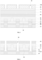
FIG. 2 is a schematic diagram of forming a substrate and a transistor in the method for manufacturing a semiconductor structure according to an exemplary embodiment. -
FIG. 3 is a schematic diagram of forming a first opening in the method for manufacturing a semiconductor structure according to an exemplary embodiment. -
FIG. 4 is a schematic diagram of forming an initial oxide layer in the method for manufacturing a semiconductor structure according to an exemplary embodiment. -
FIG. 5 is a schematic diagram of forming an oxide layer and a second opening in the method for manufacturing a semiconductor structure according to an exemplary embodiment. -
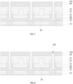
FIG. 6 is a schematic diagram of forming a release hole in the method for manufacturing a semiconductor structure according to an exemplary embodiment. -
FIG. 7 is a schematic diagram of forming a second initial dielectric layer in the method for manufacturing a semiconductor structure according to an exemplary embodiment. -
FIG. 8 is a schematic diagram of forming a second dielectric layer and an intermediate hole in the method for manufacturing a semiconductor structure according to an exemplary embodiment. -
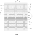
FIG. 9 is a schematic diagram of forming a conductive structure in the method for manufacturing a semiconductor structure and a schematic diagram of a semiconductor structure according to an exemplary embodiment. - In order to make the objectives, technical solutions and advantages of the embodiments of the present disclosure clearer, the following clearly and completely describes the technical solutions in the embodiments of the present disclosure with reference to the accompanying drawings in the embodiments of the present disclosure. Apparently, the described embodiments are only part of the embodiments of the present disclosure, not all of them. All other embodiments obtained by those skilled in the art based on the embodiments of the present disclosure without any creative efforts shall fall within the protection scope of the present disclosure. It should be noted that the embodiments in the present disclosure and the features in the embodiments can be combined with each other on a non-conflict basis.
- A floating gate effect may occur between a transistor and a substrate in a semiconductor structure, and the floating gate effect will affect the performance of the semiconductor structure. After search, the inventorfound, this is because, when the transistor is in an off state, some charges in the capacitor structure move into the transistor through a capacitor contact structure and a capacitor pad, as a result, holes in the transistor are increased to increase the voltage in the transistor, and a voltage difference is produced between the transistor and the substrate to produce the floating gate effect.
- In view of the above technical problems, in the method for manufacturing a semiconductor structure and the semiconductor structure provided by the embodiments of the present disclosure, a conductive structure is formed in the substrate, one end of the conductive structure is connected to the transistor, and when there are excess holes in the transistor, the holes can be transferred to the outside of the substrate by the conductive structure, thereby avoiding the floating gate effect between the substrate and the transistor and improving the performance of the semiconductor structure.
- An exemplary embodiment of the present disclosure provides a method for manufacturing a semiconductor structure, as shown in
FIG. 1. FIG. 1 shows a flowchart of a method for manufacturing a semiconductor structure according to an exemplary embodiment of the present disclosure, andFIGS. 2 to 10 are schematic diagrams of various stages of the method for manufacturing a semiconductor structure. The method for manufacturing a semiconductor structure will be introduced below in conjunction withFIGS. 2 to 10. - This embodiment does not limit the semiconductor structure. The following will introduce the semiconductor structure by taking a Dynamic Random Access Memory (DRAM) as an example, but this embodiment is not limited to this. The semiconductor structure in this embodiment may also be other structure.
- As shown in
FIG. 1 , a method for manufacturing a semiconductor structure provided by an exemplary embodiment of the present disclosure includes the following steps:
Step S100: a substrate is provided, the substrate having a first surface and a second surface opposite to each other, and transistors being arranged on the second surface. - Exemplarily, as shown in
FIG. 2 andFIG. 9 , thesubstrate 10 is used as a support component of the dynamic random access memory to support other components disposed thereon. Thesubstrate 10 may be made of a semiconductor material, and the semiconductor material may be one or more of silicon, germanium, a silicon-germanium compound and a silicon-carbon compound. - In a direction perpendicular to the
substrate 10, that is, the Y direction shown in the figures, thesubstrate 10 has afirst surface 101 and asecond surface 102 opposite to each other, wherein thefirst surface 101 may be understood as a top surface of thesubstrate 10, and thesecond surface 102 may be understood as a bottom surface of thesubstrate 10. - Exemplarily, as shown in
FIG. 2 , aninitial substrate 11 is provided, theinitial substrate 11 having a firstinitial surface 111 and asecond surface 102 opposite to each other; - In a vertical direction where the first
initial surface 111 points to thesecond surface 102, part of the thickness of theinitial substrate 11 is removed, the surface of the remaining of theinitial substrate 11 forms thefirst surface 101, and the remaining of theinitial substrate 11 forms thesubstrate 10. - That is, the first
initial surface 111 may be planarized using a chemical mechanical polishing process, and remove part of the thickness of theinitial substrate 11, the remaining of theinitial substrate 11 forms thesubstrate 10, and the planarized firstinitial surface 111 forms thefirst surface 101. - In this embodiment, a
transistor 20 is further arranged on thesecond surface 102. For example, anisolation structure 30 may be formed on the second surface through a deposition process, then theisolation structure 30 is patterned to form a plurality of trenches in theisolation structure 30, the trenches are arranged at intervals in a first direction, that is, the X direction shown inFIG. 2 , abit line structure 50 is formed in each trench, and a plurality of active columns arranged in an array are formed on thebit line structures 50. - After the active columns are formed, a
word line 40 extending in the first direction is formed on theisolation structure 30, part of theword line 40 wraps achannel region 22 of each active column, and each active column and theword line 40 wrapping the active column constitute atransistor 20. - An
air gap layer 31 is further formed in theisolation structure 30. - Step S200, release holes are formed in the substrate, the release holes extending into the transistors, bottoms of the release holes being located in channel regions of the transistors, and top surfaces of the release holes being flush with the first surface.
- Illustratively, as shown in
FIG. 3 , amask layer 70 is formed on thefirst surface 101. Themask layer 70 may be formed on thefirst surface 101 by a deposition process. - It should be noted that, in this embodiment, the
mask layer 70 may be a single film layer or a laminated structure. When themask layer 70 includes a laminated structure, the mask layer may include afirst mask layer 71 and asecond mask layer 72 laminated, thefirst mask layer 71 is arranged on afirst dielectric layer 60, and thefirst dielectric layer 60 may include a silicon oxide layer, wherein the material of thefirst mask layer 71 is different from the material of thesecond mask layer 72, for example, the material of thefirst mask layer 71 may include amorphous carbon, and the material of thesecond mask layer 72 may include silicon oxynitride. - After the
mask layer 70 is formed, aphotoresist layer 80 may be formed on themask layer 70 by coating, and then the photoresist layer is patterned by exposure, development, or etching to form a mask pattern in thephotoresist layer 80, wherein the mask pattern includes a plurality offirst openings 81 and bumps 82 for separating thefirst openings 81, the number of thefirst openings 81 corresponds to the number of thetransistors 20 one to one, and the projection of thefirst opening 81 in thetransistor 20 is located in asource 21 of thetransistor 20. - As shown in
FIG. 5 , anoxide layer 100 is formed on side walls of thefirst openings 81, theoxide layer 100 extends to the outside of thefirst openings 81 and cover the top surface of themask layer 70, and theoxide layer 100 located in thefirst openings 81 enclosessecond openings 83, wherein theoxide layer 100 may be a silicon oxide layer. - For example, as shown in
FIG. 4 , aninitial oxide layer 110 may be formed on the side walls and bottom walls of thefirst openings 81 by an atomic layer deposition process, and theinitial oxide layer 110 extends to the outside of thefirst openings 81 and covers the top surface of themask layer 70. - Then, the
initial oxide layer 110 located on the bottom walls of thesecond openings 83 is removed with an etching gas or etching solution, and the remaining of theinitial oxide layer 110 forms theoxide layer 100, that is, the formedoxide layer 100 covers the top surfaces and side walls of thebumps 82, wherein theoxide layer 100 located in thefirst openings 81 encloses thesecond openings 83. - In this embodiment, the
oxide layer 100 is formed to reduce the diameter of thefirst openings 81, thereby reducing the diameter of the release holes 90, reducing excessive damage to thetransistors 20 by the release holes 90, and ensuring the performance of thetransistors 20. - Finally, the
mask layer 70, thesubstrate 10, thesources 21 of thetransistors 20 and part of thechannel regions 22 of thetransistors 20 that are exposed in thesecond openings 83 are removed with the etching solution or etching gas, to form the release holes 90, as shown inFIG. 6 . - It should be noted that, in this embodiment, a part of the release holes 90 are located in the
transistors 20, and the other part are located in thesubstrate 10. In addition, in some embodiments, after the release holes 90 are formed, thephotoresist layer 80, themask layer 70 and theoxide layer 100 need to be removed by dry or wet etching. - In this embodiment, the
mask layer 70 is of a laminated structure. During pattern transfer, thesecond mask layer 72 may be first etched with the mask pattern formed by thebumps 82 covered with theoxide layer 100 as a mask, and form a patternedsecond mask layer 72, and then thefirst mask layer 71, thesubstrate 10 and thetransistors 20 continue to be etched with the patternedsecond mask layer 72 as a mask, to form the release holes 90. - In this embodiment, multiple times of pattern transfer can ensure the accuracy of the pattern finally transferred to the
substrate 10 and thetransistors 20, and improve the accuracy of therelease hole 90. - In some embodiments, after the providing a
substrate 10 and before the forming amask layer 70 on thefirst surface 101, the method for manufacturing a semiconductor structure further includes forming afirst dielectric layer 60 on thefirst surface 101, that is, thefirst dielectric layer 60 is arranged between thefirst surface 101 and themask layer 70. - In this embodiment, the
first dielectric layer 60 is arranged on thefirst surface 101 to protect thesubstrate 10, which can reduce lateral etching of thesubstrate 10 when the release holes 90 are formed, to improve the performance of the semiconductor structure. - Step S300, a conductive structure is formed in the release holes, the conductive structure extending to the outside of the release holes and covering the first surface of the substrate.
- Exemplarily, as shown in
FIG. 7 , first, a secondinitial dielectric layer 131 is formed in the release holes 90 by an atomic layer deposition process, the secondinitial dielectric layer 131 extending to the outside of the release holes 90 and covering thefirst dielectric layer 60. - Then, the second
initial dielectric layer 131 on thefirst dielectric layer 60 and the secondinitial dielectric layer 131 on the bottom of the release holes 90 are removed with an etching solution or etching gas, the remaining of the secondinitial dielectric layer 131 forms asecond dielectric layer 130, and thesecond dielectric layer 130 enclosesintermediate holes 140 in the release holes 90, as shown inFIG. 8 . - As shown in
FIG. 9 , theconductive structure 150 is formed in the intermediate holes by a deposition process, theconductive structure 150 extending to the outside of theintermediate holes 140 and covering thefirst dielectric layer 60, wherein the material of theconductive structure 150 may include conductive materials such as copper, aluminum or tungsten. - It should be noted that, in this embodiment, the deposition process may include an atomic layer deposition process, a physical vapor deposition process, or a chemical vapor deposition process.
- In the method for manufacturing a semiconductor structure and the semiconductor structure provided by the embodiments of the present disclosure, a conductive structure is formed in the substrate, one end of the conductive structure is connected to the transistors, and when there are excess holes in the transistors, the holes can be transferred to the outside of the substrate by the conductive structure, thereby avoiding the floating gate effect between the substrate and the transistors and improving the performance of the semiconductor structure.
- As shown in
FIG. 9 , an embodiment of the present disclosure further provides a semiconductor structure, including: - a
substrate 10, thesubstrate 10 having afirst surface 101 and asecond surface 102 opposite to each other, a plurality oftransistors 20 being arranged on thesecond surface 102, and the plurality oftransistors 20 being arranged in an array; and - a
conductive structure 150, wherein theconductive structure 150 includes aconductive body 151 and a plurality ofconductive bumps 152 arranged on theconductive body 151, theconductive body 151 is arranged on thefirst surface 101, each of theconductive bumps 152 corresponds to onetransistor 20, and the ends of theconductive bumps 152 away from theconductive body 151 pass through thesubstrate 10 andsources 21 of thetransistors 20 and then are communicated withchannel regions 22 of thetransistors 20. - The material of the
conductive body 151 and the material of theconductive bumps 152 are metal materials, for example, the materials of theconductive body 151 and theconductive bumps 152 may include one of copper, aluminum, or tungsten. - In the semiconductor structure provided by the embodiments of the present disclosure, a conductive structure is formed in the substrate, one end of the conductive structure is connected to the channel regions of the transistors, and when there are excess holes in the transistor, the holes can be transferred to the outside of the substrate by the conductive structure, thereby avoiding the floating gate effect between the substrate and the transistors and improving the performance of the semiconductor structure.
- In some embodiments, the semiconductor structure further includes a
first dielectric layer 60, thefirst dielectric layer 60 is arranged between thefirst surface 101 and theconductive body 151, and the ends of theconductive bumps 152 away from theconductive body 151 penetrate thefirst dielectric layer 60 and then are communicated with thechannel regions 22 of thetransistors 20, wherein the material of thefirst dielectric layer 60 may include silicon oxide. - In this embodiment, the
first dielectric layer 60 can avoid electrical connection of theconductive body 151 to other devices arranged in thesubstrate 10, which ensures normal use of the semiconductor structure. - In some embodiments, the semiconductor structure further includes a
second dielectric layer 130, and thesecond dielectric layer 130 is arranged on the surfaces of theconductive bumps 152, wherein the material of thesecond dielectric layer 130 may include silicon nitride. - In this embodiment, the
second dielectric layer 130 can avoid electrical connection of theconductive bump 152 to adrain 23 of thetransistor 20 or other devices arranged in thesubstrate 10, which ensures the performance of the semiconductor structure. - In some embodiments, the
substrate 10 is provided with a plurality ofbit line structures 50 arranged in a row direction of thetransistors 20, the top surfaces of thebit line structures 50 are located on thesecond surface 102, and thesources 21 of thetransistors 20 are connected to thebit line structures 50. - It should be noted that, in this embodiment, the row direction of the
transistors 20 may be the X direction shown in the figures. - The plurality of
bit line structures 50 may be arranged at intervals in the row direction of thetransistors 20, and thebit line structures 50 may extend in a column direction of thetransistors 20, that is, thebit line structures 50 may extend in a direction perpendicular to the X direction. - In some embodiments, the
substrate 10 is formed with a plurality ofword lines 40 arranged in the column direction of thetransistors 20, and the word lines 40 are configured to connect thechannel regions 22 of the plurality oftransistors 20. - A third dielectric layer and an isolation layer stacked are formed on the word lines 40, the third dielectric layer abuts against the word lines 40, the third dielectric layer includes a silicon oxide layer, and the isolation layer includes a silicon nitride layer.
- In some embodiments, a
capacitor contact structure 160 is connected to thedrain 23 of one of thetransistor 20, and acapacitor structure 170 is connected to thecapacitor contact structure 160, wherein thecapacitor structure 170 includes antop electrode 171, adielectric layer 172 and abottom electrode 173, and acapacitor pad 180 may be connected to thebottom electrode 173. - It should be noted that the
capacitor structure 170 and thecapacitor contact structure 160 are further provided with a plurality of support layers and third dielectric layers alternately arranged in sequence. - Exemplarily, the
capacitor contact structure 160 includes afirst contact structure 161 and asecond contact structure 162 adhered, the end of thefirst contact structure 161 away from thesecond contact structure 162 is connected to thedrain 23 of one of thetransistor 20, and the end of thesecond contact structure 162 away from thefirst contact structure 161 is connected to one of thecapacitor structure 170. - This embodiment realizes the connection between the capacitor structure and the drains of the transistors through the capacitor contact structure. During actual application, when data needs to be written into the capacitor structure, a voltage is applied to the word lines to open the channel regions of the transistors, so that the sources of the transistors are connected to the drains. At this time, the data on the word lines is transmitted to the drains by the sources, and then transmitted to the capacitor structure by the capacitor contact structure for storage.
- In this embodiment, the
first contact structure 161 may be in a regular shape, for example, a rectangular shape or a cylindrical shape, or in an irregular shape. - Exemplarily, the
first contact structure 161 includes afirst segment 1611 and asecond segment 1612 connected to thefirst segment 1611, the end of thefirst segment 1611 away from thesecond segment 1612 is connected to thedrain 23, and the end of thesecond segment 1612 away from thefirst segment 1611 is connected to thesecond contact structure 162. - Taking a plane perpendicular to the
substrate 10 as the longitudinal section, the longitudinal section of thefirst segment 1611 is a rectangle, and the longitudinal section of thesecond segment 1612 is a trapezoid enlarged from top to bottom, which can increase the area of thefirst contact structure 161 to reduce the resistance of thefirst contact structure 161 and improve the sensitivity of signal transmission. - The
second contact structure 162 includes athird segment 1621 and afourth segment 1622 connected to thethird segment 1621, the end of thethird segment 1621 away from thefourth segment 1622 is connected to thefirst contact structure 161, and the end of thefourth segment 1622 away from thethird segment 1621 is connected to one end of thecapacitor structure 170. - Taking the plane perpendicular to the
substrate 10 as the longitudinal section, the longitudinal section of thethird segment 1621 is a trapezoid reduced from top to bottom, and the longitudinal section of thefourth segment 1622 is a rectangle, which can enlarge the contact area between thesecond contact structure 162 and thefirst contact structure 161 to reduce the contact resistance and improve the sensitivity of signal transmission. - In some embodiments, the
first contact structure 161 has a first surface and a second surface opposite to each other, that is, the first surface forms one end of thefirst segment 1611, and the second segment forms the end of thesecond segment 1612 away from thefirst segment 1611. Thesecond contact structure 162 has a third surface and a fourth surface opposite to each other, that is, the third surface forms one end of thethird segment 1621, and the fourth surface forms the end of thefourth segment 1622 away from thethird segment 1621. The second surface is connected to thedrain 23 of one of thetransistor 20, the first surface is connected to the third surface, and the fourth surface is connected to one of thecapacitor structure 170. The projection area of the first surface on thesubstrate 10 is larger than the projection area of the third surface on thesubstrate 10, which facilitates the alignment of thefirst contact structure 161 and thesecond contact structure 162. - In the semiconductor structure provided by the embodiments of the present disclosure, a conductive structure is formed in the substrate, one end of the conductive structure is connected to one of the channel region of the transistor, and when there are excess holes in the transistor, the holes can be transferred to the outside of the substrate by the conductive structure, thereby avoiding the floating gate effect between the substrate and the transistor and improving the performance of the semiconductor structure.
- The embodiments or implementations in this specification are described in a progressive manner, each embodiment focuses on the differences from other embodiments, and the same or similar parts between the various embodiments may be referred to each other.
- In the description of this specification, the descriptions with reference to the terms "embodiment", "exemplary embodiment", "some implementations", "schematic implementation", "example", etc. mean that specific features, structures, materials or characteristics described in conjunction with the embodiments or examples are included in at least one embodiment or example of the present application.
- In this specification, the schematic descriptions of the above terms do not necessarily refer to the same embodiment or example. Moreover, the described specific features, structures, materials or characteristics may be combined in an appropriate manner in any one or more embodiments or examples.
- In the description of the present disclosure, it should be noted that the orientations or positional relationships indicated by the terms "center", "upper", "lower", "left", "right", "vertical", "horizontal", "inner", "outer", etc. are based on the orientations or positional relationships shown in the accompanying drawings, and are intended to facilitate the description of the present disclosure and simplify the description only, rather than indicating or implying that the device or element referred to must have a particular orientation or be constructed and operated in a particular orientation, and will not to be interpreted as limiting the present disclosure.
- It can be understood that the terms "first", "second", etc. used in the present disclosure can be used in the present disclosure to describe various structures, but these structures are not limited by these terms. These terms are only configured to distinguish the first structure from another structure.
- In one or more drawings, the same elements are represented by similar reference numerals. For the sake of clarity, various parts in the drawings are not drawn to scale. In addition, some well-known parts may not be shown. For the sake of brevity, the structure obtained after several steps can be described in one figure. Many specific details of the present disclosure are described below, such as the structure, material, dimension, treatment process and technology of devices, in order to understand the present disclosure more clearly. However, as those skilled in the art can understand, the present disclosure may not be implemented according to these specific details.
- Finally, it should be noted that the above embodiments are merely configured to describe, but not to limit, the technical solutions of the present disclosure. Although the present disclosure is described in detail with reference to the above embodiments, those of ordinary skill in the art should understand that various modifications may be made to the technical solutions described in the foregoing embodiments, or equivalent substitutions may be made to some or all technical features thereof, and these modifications or substitutions do not make the essences of the corresponding technical solutions depart from the scope of the technical solutions of the embodiments of the present disclosure.
- In the method for manufacturing a semiconductor structure and the semiconductor structure provided by the embodiments of the present disclosure, a conductive structure is formed in the substrate, one end of the conductive structure is connected to the transistor, and when there are excess holes in the transistor, the holes can be transferred to the outside of the substrate by the conductive structure, thereby avoiding the floating gate effect between the substrate and the transistor and improving the performance of the semiconductor structure.
| 10 - | substrate; | 11 - | initial substrate; |
| 20 - | transistor; | 21 - | source; |
| 22 - | channel region; | 23 - | drain; |
| 30 - | isolation structure; | 31 - | air gap layer; |
| 40 - | word line; | 50 - | bit line structure; |
| 60 - | first dielectric layer; | 70 - | mask layer; |
| 71 - | first mask layer; | 72 - | second mask layer; |
| 80 - | photoresist layer; | 81 - | first opening; |
| 82 - | bump; | 83 - | second opening; |
| 90 - | release hole; | 100 | - oxide layer; |
| 110 - | initial oxide layer; | 130 - | second dielectric layer; |
| 131 - | second initial dielectric layer; | 140 - | intermediate hole; |
| 150 - | conductive structure; | 151 - | conductive body; |
| 152 - | conductive bump; | 160 - | capacitor contact structure; |
| 161 - | first contact structure; | 162 - | second contact structure; |
| 1611 - | first segment; | 1612 - | second segment; |
| 1621 - | third segment; | 1622 - | fourth segment; |
| 170 - | capacitor structure; | 171 - | upper electrode; |
| 172 - | dielectric layer; | 173 - | lower electrode; |
| 180 - | capacitor pad. |
Claims (15)
- A method for manufacturing a semiconductor structure,comprising:providing a substrate, the substrate having a first surface and a second surface opposite to each other, and transistors being arranged on the second surface;forming release holes in the substrate, the release holes extending into the transistors, bottoms of the release holes being located in channel regions of the transistors, and top surfaces of the release holes being flush with the first surface; andforming a conductive structure in the release holes, the conductive structure extending to the outside of the release holes and covering the first surface of the substrate.
- The method for manufacturing the semiconductor structure according to claim 1, wherein the providing the substrate comprises:providing an initial substrate, the initial substrate having a first initial surface and the second surface opposite to each other; andin a vertical direction where the first initial surface points to the second surface, removing part of the thickness of the initial substrate, a surface of a remaining of the initial substrate forming the first surface, and a remaining of the initial substrate forming the substrate.
- The method for manufacturing the semiconductor structure according to claim 2, wherein the removing part of the initial substrate along the first initial surface comprises:
planarizing the first initial surface by a chemical mechanical polishing process, and removing part of a thickness of the initial substrate. - The method for manufacturing the semiconductor structure according to claim 1, wherein the forming the release hole in the substrate comprises:forming a mask layer on the first surface;forming a photoresist layer on the mask layer, and patterning the photoresist layer to form a mask pattern in the photoresist layer, the mask pattern comprising a plurality of first openings and bumps for separating the first openings, and projections of the first openings in the transistors being located in sources of the transistors; andremoving the mask layer, the substrate, the sources of the transistors and part of the channel regions of the transistors that are exposed in the first opening, to form the release holes.
- The method for manufacturing the semiconductor structure according to claim 4, wherein the removing the mask layer, the substrate, the sources of the transistors and part of the channel regions of the transistors that are exposed in the first openings, to form the release holes comprises:forming an oxide layer on side walls of the first openings, the oxide layer extending to the outside of the first openings and covering a top surface of the mask layer, and the oxide layer located in the first openings enclosing second openings; andremoving the mask layer, the substrate, the sources of the transistors and part of the channel regions of the transistors that are exposed in the second openings, to form the release holes.
- The method for manufacturing the semiconductor structure according to claim 5, wherein before the forming the mask layer on the first surface, the method for manufacturing the semiconductor structure comprises:
forming a first dielectric layer on the first surface. - The method for manufacturing the semiconductor structure according to claim 6, wherein the forming the mask layer on the first surface comprises:
forming a first mask layer and a second mask layer sequentially stacked on the first dielectric layer, materials of the first mask layer and the second mask layer being different. - The method for manufacturing the semiconductor structure according to claim 7, wherein the forming a conductive structure in the release holes comprises:forming a second initial dielectric layer in the release holes, the second initial dielectric layer extending to outside of the release holes and covering the first dielectric layer;removing the second initial dielectric layer on the first dielectric layer and the second initial dielectric layer on bottoms of the release holes, a remaining of the second initial dielectric layer forming a second dielectric layer, and the second dielectric layer enclosing intermediate holes in the release holes; andforming a conductive structure in the intermediate holes, the conductive structure extending to outside of the intermediate holes and covering the first dielectric layer.
- A semiconductor structure, comprising:a substrate, the substrate having a first surface and a second surface opposite to each other, a plurality of transistors being arranged on the second surface, and the transistors being arranged in an array; anda conductive structure, the conductive structure comprising a conductive body and a plurality of conductive bumps arranged on the conductive body, the conductive body being arranged on the first surface, each of the conductive bumps corresponds to one transistor, and ends of the conductive bumps away from the conductive body passing through the substrate and sources of the transistors and then being communicated with channel regions of the transistors.
- The semiconductor structure according to claim 9, wherein amaterial of the conductive body and a material of the conductive bumps both comprise one of copper, aluminum, and tungsten.
- The semiconductor structure according to claim 9, wherein the substrate is provided with a plurality of bit line structures arranged in a row direction of the transistors, top surfaces of the bit line structures are located on the second surface, and the sources of the transistors are connected to the bit line structures.
- The semiconductor structure according to claim 9, wherein the substrate is formed with a plurality of word lines arranged in a column direction of the transistors, and the word lines are configured to connect the channel regions of the plurality of transistors.
- The semiconductor structure according to any one of claims 9-12, wherein capacitor contact structures are connected to drains of the transistors, and capacitor structures are connected to the capacitor contact structures.
- The semiconductor structure according to claim 13, wherein each of the capacitor contact structures comprises a first contact structure and a second contact structure adhered, an end of the first contact structure away from the second contact structure is connected to the drain of one of the transistor, and an end of the second contact structure away from the first contact structure is connected to one of the capacitor structure.
- The semiconductor structure according to claim 14, wherein the first contact structure has a first surface and a second surface opposite to each other, and the second contact structure has a third surface and a fourth surface opposite to each other, wherein the second surface is connected to the drain of one of the transistor, the first surface is connected to the third surface, the fourth surface is connected to one of the capacitor structure, and a projection area of the first surface on the substrate is larger than a projection area of the third surface on the substrate.
Applications Claiming Priority (2)
| Application Number | Priority Date | Filing Date | Title |
|---|---|---|---|
| CN202110812549.0A CN115643747B (en) | 2021-07-19 | 2021-07-19 | Semiconductor structure manufacturing method and semiconductor structure |
| PCT/CN2021/108950 WO2023000360A1 (en) | 2021-07-19 | 2021-07-28 | Manufacturing method for semiconductor structure, and semiconductor structure |
Publications (3)
| Publication Number | Publication Date |
|---|---|
| EP4220685A1 true EP4220685A1 (en) | 2023-08-02 |
| EP4220685A4 EP4220685A4 (en) | 2024-04-24 |
| EP4220685B1 EP4220685B1 (en) | 2025-04-23 |
Family
ID=84939537
Family Applications (1)
| Application Number | Title | Priority Date | Filing Date |
|---|---|---|---|
| EP21950608.6A Active EP4220685B1 (en) | 2021-07-19 | 2021-07-28 | Method for manufacturing semiconductor structure and semiconductor structure |
Country Status (4)
| Country | Link |
|---|---|
| US (1) | US11864371B2 (en) |
| EP (1) | EP4220685B1 (en) |
| CN (1) | CN115643747B (en) |
| WO (1) | WO2023000360A1 (en) |
Family Cites Families (11)
| Publication number | Priority date | Publication date | Assignee | Title |
|---|---|---|---|---|
| US6355950B1 (en) * | 1998-09-23 | 2002-03-12 | Intel Corporation | Substrate interconnect for power distribution on integrated circuits |
| US20050274604A1 (en) * | 2004-02-06 | 2005-12-15 | Koji Saito | Plating apparatus |
| US7075133B1 (en) * | 2004-05-03 | 2006-07-11 | National Semiconductor Corporation | Semiconductor die with heat and electrical pipes |
| US7498622B1 (en) | 2007-12-14 | 2009-03-03 | International Business Machines Corporation | Latchup robust gate array using through wafer via |
| US8017471B2 (en) * | 2008-08-06 | 2011-09-13 | International Business Machines Corporation | Structure and method of latchup robustness with placement of through wafer via within CMOS circuitry |
| JP5438980B2 (en) * | 2009-01-23 | 2014-03-12 | ラピスセミコンダクタ株式会社 | Manufacturing method of semiconductor device |
| CN102544049B (en) | 2010-12-22 | 2014-04-16 | 中国科学院微电子研究所 | Three-dimensional semiconductor memory device and its manufacturing method |
| CN103258797B (en) * | 2012-02-21 | 2016-01-20 | 中芯国际集成电路制造(上海)有限公司 | The manufacture method of separate gate flash memory unit |
| JP2015060895A (en) | 2013-09-17 | 2015-03-30 | 株式会社東芝 | Semiconductor device |
| JP6910944B2 (en) * | 2017-12-27 | 2021-07-28 | ルネサスエレクトロニクス株式会社 | Semiconductor device |
| CN113053900B (en) * | 2021-03-22 | 2023-01-20 | 长鑫存储技术有限公司 | Semiconductor structure and manufacturing method thereof |
-
2021
- 2021-07-19 CN CN202110812549.0A patent/CN115643747B/en active Active
- 2021-07-28 US US17/603,949 patent/US11864371B2/en active Active
- 2021-07-28 EP EP21950608.6A patent/EP4220685B1/en active Active
- 2021-07-28 WO PCT/CN2021/108950 patent/WO2023000360A1/en not_active Ceased
Also Published As
| Publication number | Publication date |
|---|---|
| WO2023000360A1 (en) | 2023-01-26 |
| EP4220685A4 (en) | 2024-04-24 |
| US11864371B2 (en) | 2024-01-02 |
| US20230121343A1 (en) | 2023-04-20 |
| CN115643747A (en) | 2023-01-24 |
| EP4220685B1 (en) | 2025-04-23 |
| CN115643747B (en) | 2025-10-21 |
Similar Documents
| Publication | Publication Date | Title |
|---|---|---|
| US8274112B2 (en) | Semiconductor memory device having pillar structures | |
| CN103270593B (en) | For dynamic random access memory (DRAM) rectangular capacitors and form its dual photoetching method | |
| US6489195B1 (en) | Method for fabricating DRAM cell using a protection layer | |
| US8486831B2 (en) | Semiconductor device manufacturing method | |
| US6903404B2 (en) | Semiconductor memory device and method for manufacturing the same | |
| KR970000718B1 (en) | Semiconductor memory device and manufacturing method thereof | |
| TWI802997B (en) | Semiconductor structure and method of manufacturing thereof | |
| KR19990073712A (en) | Semiconductor memory device provided with COB and manufacturing method thereof | |
| US6156608A (en) | Method of manufacturing cylindrical shaped capacitor | |
| US6352896B1 (en) | Method of manufacturing DRAM capacitor | |
| KR101400061B1 (en) | Capacitor, semiconductor device including the capacitor, method of forming the capacitor and method of manufacturing the semiconductor device including the capacitor | |
| US5913129A (en) | Method of fabricating a capacitor structure for a dynamic random access memory | |
| US6844229B2 (en) | Method of manufacturing semiconductor device having storage electrode of capacitor | |
| US7145195B2 (en) | Semiconductor memory device and method of manufacturing the same | |
| EP4220685B1 (en) | Method for manufacturing semiconductor structure and semiconductor structure | |
| EP4086959B1 (en) | Preparation method for semiconductor structure and semiconductor structure | |
| US20060148168A1 (en) | Process for fabricating dynamic random access memory | |
| JP2602581B2 (en) | Method for manufacturing semiconductor memory device | |
| KR20010108963A (en) | DRAM device having fence surrounding cell aray region and manufacturing method thereof | |
| CN116017976B (en) | Semiconductor structure and its preparation method | |
| CN119451104B (en) | A patterning method | |
| US12082393B2 (en) | Method for manufacturing memory and memory | |
| US12588191B2 (en) | Semiconductor device and method of fabricating the same | |
| KR100252882B1 (en) | Manufacturing Method of Semiconductor Device | |
| GB2244596A (en) | Semiconductor memory device with stacked capacitor |
Legal Events
| Date | Code | Title | Description |
|---|---|---|---|
| STAA | Information on the status of an ep patent application or granted ep patent |
Free format text: STATUS: THE INTERNATIONAL PUBLICATION HAS BEEN MADE |
|
| PUAI | Public reference made under article 153(3) epc to a published international application that has entered the european phase |
Free format text: ORIGINAL CODE: 0009012 |
|
| STAA | Information on the status of an ep patent application or granted ep patent |
Free format text: STATUS: REQUEST FOR EXAMINATION WAS MADE |
|
| 17P | Request for examination filed |
Effective date: 20230425 |
|
| AK | Designated contracting states |
Kind code of ref document: A1 Designated state(s): AL AT BE BG CH CY CZ DE DK EE ES FI FR GB GR HR HU IE IS IT LI LT LU LV MC MK MT NL NO PL PT RO RS SE SI SK SM TR |
|
| REG | Reference to a national code |
Ref legal event code: R079 Ipc: H10B0012000000 Ref country code: DE Ref document number: 602021029831 Country of ref document: DE Free format text: PREVIOUS MAIN CLASS: H99Z9999999999 |
|
| A4 | Supplementary search report drawn up and despatched |
Effective date: 20240326 |
|
| RIC1 | Information provided on ipc code assigned before grant |
Ipc: H10B 12/00 20230101AFI20240321BHEP |
|
| DAV | Request for validation of the european patent (deleted) | ||
| DAX | Request for extension of the european patent (deleted) | ||
| GRAP | Despatch of communication of intention to grant a patent |
Free format text: ORIGINAL CODE: EPIDOSNIGR1 |
|
| STAA | Information on the status of an ep patent application or granted ep patent |
Free format text: STATUS: GRANT OF PATENT IS INTENDED |
|
| INTG | Intention to grant announced |
Effective date: 20250120 |
|
| GRAS | Grant fee paid |
Free format text: ORIGINAL CODE: EPIDOSNIGR3 |
|
| P01 | Opt-out of the competence of the unified patent court (upc) registered |
Free format text: CASE NUMBER: APP_7111/2025 Effective date: 20250212 |
|
| GRAA | (expected) grant |
Free format text: ORIGINAL CODE: 0009210 |
|
| STAA | Information on the status of an ep patent application or granted ep patent |
Free format text: STATUS: THE PATENT HAS BEEN GRANTED |
|
| AK | Designated contracting states |
Kind code of ref document: B1 Designated state(s): AL AT BE BG CH CY CZ DE DK EE ES FI FR GB GR HR HU IE IS IT LI LT LU LV MC MK MT NL NO PL PT RO RS SE SI SK SM TR |
|
| REG | Reference to a national code |
Ref country code: GB Ref legal event code: FG4D |
|
| REG | Reference to a national code |
Ref country code: CH Ref legal event code: EP |
|
| REG | Reference to a national code |
Ref country code: DE Ref legal event code: R096 Ref document number: 602021029831 Country of ref document: DE |
|
| REG | Reference to a national code |
Ref country code: IE Ref legal event code: FG4D |
|
| REG | Reference to a national code |
Ref country code: NL Ref legal event code: MP Effective date: 20250423 |
|
| PG25 | Lapsed in a contracting state [announced via postgrant information from national office to epo] |
Ref country code: NL Free format text: LAPSE BECAUSE OF FAILURE TO SUBMIT A TRANSLATION OF THE DESCRIPTION OR TO PAY THE FEE WITHIN THE PRESCRIBED TIME-LIMIT Effective date: 20250423 |
|
| REG | Reference to a national code |
Ref country code: AT Ref legal event code: MK05 Ref document number: 1789109 Country of ref document: AT Kind code of ref document: T Effective date: 20250423 |
|
| PG25 | Lapsed in a contracting state [announced via postgrant information from national office to epo] |
Ref country code: FI Free format text: LAPSE BECAUSE OF FAILURE TO SUBMIT A TRANSLATION OF THE DESCRIPTION OR TO PAY THE FEE WITHIN THE PRESCRIBED TIME-LIMIT Effective date: 20250423 Ref country code: ES Free format text: LAPSE BECAUSE OF FAILURE TO SUBMIT A TRANSLATION OF THE DESCRIPTION OR TO PAY THE FEE WITHIN THE PRESCRIBED TIME-LIMIT Effective date: 20250423 Ref country code: PT Free format text: LAPSE BECAUSE OF FAILURE TO SUBMIT A TRANSLATION OF THE DESCRIPTION OR TO PAY THE FEE WITHIN THE PRESCRIBED TIME-LIMIT Effective date: 20250825 |
|
| PGFP | Annual fee paid to national office [announced via postgrant information from national office to epo] |
Ref country code: DE Payment date: 20250722 Year of fee payment: 5 |
|
| REG | Reference to a national code |
Ref country code: LT Ref legal event code: MG9D |
|
| PG25 | Lapsed in a contracting state [announced via postgrant information from national office to epo] |
Ref country code: GR Free format text: LAPSE BECAUSE OF FAILURE TO SUBMIT A TRANSLATION OF THE DESCRIPTION OR TO PAY THE FEE WITHIN THE PRESCRIBED TIME-LIMIT Effective date: 20250724 Ref country code: NO Free format text: LAPSE BECAUSE OF FAILURE TO SUBMIT A TRANSLATION OF THE DESCRIPTION OR TO PAY THE FEE WITHIN THE PRESCRIBED TIME-LIMIT Effective date: 20250723 |
|
| PG25 | Lapsed in a contracting state [announced via postgrant information from national office to epo] |
Ref country code: PL Free format text: LAPSE BECAUSE OF FAILURE TO SUBMIT A TRANSLATION OF THE DESCRIPTION OR TO PAY THE FEE WITHIN THE PRESCRIBED TIME-LIMIT Effective date: 20250423 |
|
| PG25 | Lapsed in a contracting state [announced via postgrant information from national office to epo] |
Ref country code: BG Free format text: LAPSE BECAUSE OF FAILURE TO SUBMIT A TRANSLATION OF THE DESCRIPTION OR TO PAY THE FEE WITHIN THE PRESCRIBED TIME-LIMIT Effective date: 20250423 |
|
| PG25 | Lapsed in a contracting state [announced via postgrant information from national office to epo] |
Ref country code: HR Free format text: LAPSE BECAUSE OF FAILURE TO SUBMIT A TRANSLATION OF THE DESCRIPTION OR TO PAY THE FEE WITHIN THE PRESCRIBED TIME-LIMIT Effective date: 20250423 |
|
| PG25 | Lapsed in a contracting state [announced via postgrant information from national office to epo] |
Ref country code: AT Free format text: LAPSE BECAUSE OF FAILURE TO SUBMIT A TRANSLATION OF THE DESCRIPTION OR TO PAY THE FEE WITHIN THE PRESCRIBED TIME-LIMIT Effective date: 20250423 |
|
| PG25 | Lapsed in a contracting state [announced via postgrant information from national office to epo] |
Ref country code: RS Free format text: LAPSE BECAUSE OF FAILURE TO SUBMIT A TRANSLATION OF THE DESCRIPTION OR TO PAY THE FEE WITHIN THE PRESCRIBED TIME-LIMIT Effective date: 20250723 |
|
| PG25 | Lapsed in a contracting state [announced via postgrant information from national office to epo] |
Ref country code: IS Free format text: LAPSE BECAUSE OF FAILURE TO SUBMIT A TRANSLATION OF THE DESCRIPTION OR TO PAY THE FEE WITHIN THE PRESCRIBED TIME-LIMIT Effective date: 20250823 |
|
| PG25 | Lapsed in a contracting state [announced via postgrant information from national office to epo] |
Ref country code: LV Free format text: LAPSE BECAUSE OF FAILURE TO SUBMIT A TRANSLATION OF THE DESCRIPTION OR TO PAY THE FEE WITHIN THE PRESCRIBED TIME-LIMIT Effective date: 20250423 |
|
| PG25 | Lapsed in a contracting state [announced via postgrant information from national office to epo] |
Ref country code: SM Free format text: LAPSE BECAUSE OF FAILURE TO SUBMIT A TRANSLATION OF THE DESCRIPTION OR TO PAY THE FEE WITHIN THE PRESCRIBED TIME-LIMIT Effective date: 20250423 Ref country code: DK Free format text: LAPSE BECAUSE OF FAILURE TO SUBMIT A TRANSLATION OF THE DESCRIPTION OR TO PAY THE FEE WITHIN THE PRESCRIBED TIME-LIMIT Effective date: 20250423 |
|
| PG25 | Lapsed in a contracting state [announced via postgrant information from national office to epo] |
Ref country code: CZ Free format text: LAPSE BECAUSE OF FAILURE TO SUBMIT A TRANSLATION OF THE DESCRIPTION OR TO PAY THE FEE WITHIN THE PRESCRIBED TIME-LIMIT Effective date: 20250423 |
|
| PG25 | Lapsed in a contracting state [announced via postgrant information from national office to epo] |
Ref country code: EE Free format text: LAPSE BECAUSE OF FAILURE TO SUBMIT A TRANSLATION OF THE DESCRIPTION OR TO PAY THE FEE WITHIN THE PRESCRIBED TIME-LIMIT Effective date: 20250423 |
|
| REG | Reference to a national code |
Ref country code: DE Ref legal event code: R097 Ref document number: 602021029831 Country of ref document: DE |
|
| PG25 | Lapsed in a contracting state [announced via postgrant information from national office to epo] |
Ref country code: SK Free format text: LAPSE BECAUSE OF FAILURE TO SUBMIT A TRANSLATION OF THE DESCRIPTION OR TO PAY THE FEE WITHIN THE PRESCRIBED TIME-LIMIT Effective date: 20250423 |
|
| PG25 | Lapsed in a contracting state [announced via postgrant information from national office to epo] |
Ref country code: IT Free format text: LAPSE BECAUSE OF FAILURE TO SUBMIT A TRANSLATION OF THE DESCRIPTION OR TO PAY THE FEE WITHIN THE PRESCRIBED TIME-LIMIT Effective date: 20250423 |
|
| REG | Reference to a national code |
Ref country code: CH Ref legal event code: H13 Free format text: ST27 STATUS EVENT CODE: U-0-0-H10-H13 (AS PROVIDED BY THE NATIONAL OFFICE) Effective date: 20260224 |
|
| PLBE | No opposition filed within time limit |
Free format text: ORIGINAL CODE: 0009261 |
|
| STAA | Information on the status of an ep patent application or granted ep patent |
Free format text: STATUS: NO OPPOSITION FILED WITHIN TIME LIMIT |
|
| REG | Reference to a national code |
Ref country code: CH Ref legal event code: L10 Free format text: ST27 STATUS EVENT CODE: U-0-0-L10-L00 (AS PROVIDED BY THE NATIONAL OFFICE) Effective date: 20260304 |
|
| PG25 | Lapsed in a contracting state [announced via postgrant information from national office to epo] |
Ref country code: RO Free format text: LAPSE BECAUSE OF FAILURE TO SUBMIT A TRANSLATION OF THE DESCRIPTION OR TO PAY THE FEE WITHIN THE PRESCRIBED TIME-LIMIT Effective date: 20250423 |
|
| PG25 | Lapsed in a contracting state [announced via postgrant information from national office to epo] |
Ref country code: LU Free format text: LAPSE BECAUSE OF NON-PAYMENT OF DUE FEES Effective date: 20250728 |
|
| GBPC | Gb: european patent ceased through non-payment of renewal fee |
Effective date: 20250728 |
|
| REG | Reference to a national code |
Ref country code: BE Ref legal event code: MM Effective date: 20250731 |
|
| 26N | No opposition filed |
Effective date: 20260126 |
|
| PG25 | Lapsed in a contracting state [announced via postgrant information from national office to epo] |
Ref country code: GB Free format text: LAPSE BECAUSE OF NON-PAYMENT OF DUE FEES Effective date: 20250728 |
|
| PG25 | Lapsed in a contracting state [announced via postgrant information from national office to epo] |
Ref country code: BE Free format text: LAPSE BECAUSE OF NON-PAYMENT OF DUE FEES Effective date: 20250731 |
|
| PG25 | Lapsed in a contracting state [announced via postgrant information from national office to epo] |
Ref country code: FR Free format text: LAPSE BECAUSE OF NON-PAYMENT OF DUE FEES Effective date: 20250731 |
|
| PG25 | Lapsed in a contracting state [announced via postgrant information from national office to epo] |
Ref country code: CH Free format text: LAPSE BECAUSE OF NON-PAYMENT OF DUE FEES Effective date: 20250731 |