EP4220361A2 - Touch substrate and manufacturing method therefor, touch display substrate, and touch display device - Google Patents
Touch substrate and manufacturing method therefor, touch display substrate, and touch display device Download PDFInfo
- Publication number
- EP4220361A2 EP4220361A2 EP23162922.1A EP23162922A EP4220361A2 EP 4220361 A2 EP4220361 A2 EP 4220361A2 EP 23162922 A EP23162922 A EP 23162922A EP 4220361 A2 EP4220361 A2 EP 4220361A2
- Authority
- EP
- European Patent Office
- Prior art keywords
- line
- ground
- touch
- sub
- ground line
- Prior art date
- Legal status (The legal status is an assumption and is not a legal conclusion. Google has not performed a legal analysis and makes no representation as to the accuracy of the status listed.)
- Granted
Links
Images





Classifications
-
- G—PHYSICS
- G06—COMPUTING OR CALCULATING; COUNTING
- G06F—ELECTRIC DIGITAL DATA PROCESSING
- G06F3/00—Input arrangements for transferring data to be processed into a form capable of being handled by the computer; Output arrangements for transferring data from processing unit to output unit, e.g. interface arrangements
- G06F3/01—Input arrangements or combined input and output arrangements for interaction between user and computer
- G06F3/03—Arrangements for converting the position or the displacement of a member into a coded form
- G06F3/041—Digitisers, e.g. for touch screens or touch pads, characterised by the transducing means
- G06F3/044—Digitisers, e.g. for touch screens or touch pads, characterised by the transducing means by capacitive means
- G06F3/0446—Digitisers, e.g. for touch screens or touch pads, characterised by the transducing means by capacitive means using a grid-like structure of electrodes in at least two directions, e.g. using row and column electrodes
-
- G—PHYSICS
- G06—COMPUTING OR CALCULATING; COUNTING
- G06F—ELECTRIC DIGITAL DATA PROCESSING
- G06F3/00—Input arrangements for transferring data to be processed into a form capable of being handled by the computer; Output arrangements for transferring data from processing unit to output unit, e.g. interface arrangements
- G06F3/01—Input arrangements or combined input and output arrangements for interaction between user and computer
- G06F3/03—Arrangements for converting the position or the displacement of a member into a coded form
- G06F3/041—Digitisers, e.g. for touch screens or touch pads, characterised by the transducing means
- G06F3/0416—Control or interface arrangements specially adapted for digitisers
- G06F3/04164—Connections between sensors and controllers, e.g. routing lines between electrodes and connection pads
-
- G—PHYSICS
- G06—COMPUTING OR CALCULATING; COUNTING
- G06F—ELECTRIC DIGITAL DATA PROCESSING
- G06F3/00—Input arrangements for transferring data to be processed into a form capable of being handled by the computer; Output arrangements for transferring data from processing unit to output unit, e.g. interface arrangements
- G06F3/01—Input arrangements or combined input and output arrangements for interaction between user and computer
- G06F3/03—Arrangements for converting the position or the displacement of a member into a coded form
- G06F3/041—Digitisers, e.g. for touch screens or touch pads, characterised by the transducing means
- G06F3/0412—Digitisers structurally integrated in a display
-
- G—PHYSICS
- G02—OPTICS
- G02F—OPTICAL DEVICES OR ARRANGEMENTS FOR THE CONTROL OF LIGHT BY MODIFICATION OF THE OPTICAL PROPERTIES OF THE MEDIA OF THE ELEMENTS INVOLVED THEREIN; NON-LINEAR OPTICS; FREQUENCY-CHANGING OF LIGHT; OPTICAL LOGIC ELEMENTS; OPTICAL ANALOGUE/DIGITAL CONVERTERS
- G02F1/00—Devices or arrangements for the control of the intensity, colour, phase, polarisation or direction of light arriving from an independent light source, e.g. switching, gating or modulating; Non-linear optics
- G02F1/01—Devices or arrangements for the control of the intensity, colour, phase, polarisation or direction of light arriving from an independent light source, e.g. switching, gating or modulating; Non-linear optics for the control of the intensity, phase, polarisation or colour
- G02F1/13—Devices or arrangements for the control of the intensity, colour, phase, polarisation or direction of light arriving from an independent light source, e.g. switching, gating or modulating; Non-linear optics for the control of the intensity, phase, polarisation or colour based on liquid crystals, e.g. single liquid crystal display cells
- G02F1/133—Constructional arrangements; Operation of liquid crystal cells; Circuit arrangements
- G02F1/1333—Constructional arrangements; Manufacturing methods
- G02F1/13338—Input devices, e.g. touch panels
-
- G—PHYSICS
- G06—COMPUTING OR CALCULATING; COUNTING
- G06F—ELECTRIC DIGITAL DATA PROCESSING
- G06F3/00—Input arrangements for transferring data to be processed into a form capable of being handled by the computer; Output arrangements for transferring data from processing unit to output unit, e.g. interface arrangements
- G06F3/01—Input arrangements or combined input and output arrangements for interaction between user and computer
- G06F3/03—Arrangements for converting the position or the displacement of a member into a coded form
- G06F3/041—Digitisers, e.g. for touch screens or touch pads, characterised by the transducing means
- G06F3/0416—Control or interface arrangements specially adapted for digitisers
- G06F3/0418—Control or interface arrangements specially adapted for digitisers for error correction or compensation, e.g. based on parallax, calibration or alignment
-
- G—PHYSICS
- G06—COMPUTING OR CALCULATING; COUNTING
- G06F—ELECTRIC DIGITAL DATA PROCESSING
- G06F2203/00—Indexing scheme relating to G06F3/00 - G06F3/048
- G06F2203/041—Indexing scheme relating to G06F3/041 - G06F3/045
- G06F2203/04102—Flexible digitiser, i.e. constructional details for allowing the whole digitising part of a device to be flexed or rolled like a sheet of paper
-
- G—PHYSICS
- G06—COMPUTING OR CALCULATING; COUNTING
- G06F—ELECTRIC DIGITAL DATA PROCESSING
- G06F2203/00—Indexing scheme relating to G06F3/00 - G06F3/048
- G06F2203/041—Indexing scheme relating to G06F3/041 - G06F3/045
- G06F2203/04103—Manufacturing, i.e. details related to manufacturing processes specially suited for touch sensitive devices
-
- G—PHYSICS
- G06—COMPUTING OR CALCULATING; COUNTING
- G06F—ELECTRIC DIGITAL DATA PROCESSING
- G06F2203/00—Indexing scheme relating to G06F3/00 - G06F3/048
- G06F2203/041—Indexing scheme relating to G06F3/041 - G06F3/045
- G06F2203/04111—Cross over in capacitive digitiser, i.e. details of structures for connecting electrodes of the sensing pattern where the connections cross each other, e.g. bridge structures comprising an insulating layer, or vias through substrate
-
- H—ELECTRICITY
- H05—ELECTRIC TECHNIQUES NOT OTHERWISE PROVIDED FOR
- H05K—PRINTED CIRCUITS; CASINGS OR CONSTRUCTIONAL DETAILS OF ELECTRIC APPARATUS; MANUFACTURE OF ASSEMBLAGES OF ELECTRICAL COMPONENTS
- H05K1/00—Printed circuits
- H05K1/02—Details
- H05K1/0213—Electrical arrangements not otherwise provided for
- H05K1/0254—High voltage adaptations; Electrical insulation details; Overvoltage or electrostatic discharge protection ; Arrangements for regulating voltages or for using plural voltages
- H05K1/0257—Overvoltage protection
- H05K1/0259—Electrostatic discharge [ESD] protection
-
- H—ELECTRICITY
- H10—SEMICONDUCTOR DEVICES; ELECTRIC SOLID-STATE DEVICES NOT OTHERWISE PROVIDED FOR
- H10K—ORGANIC ELECTRIC SOLID-STATE DEVICES
- H10K59/00—Integrated devices, or assemblies of multiple devices, comprising at least one organic light-emitting element covered by group H10K50/00
- H10K59/40—OLEDs integrated with touch screens
Definitions
- At least one embodiment of the present disclosure relates to a touch substrate and a manufacturing method thereof, a touch display substrate and a touch display device.
- AMOLED active-matrix organic light-emitting diode
- At least one embodiment of the present disclosure relates to a touch substrate and a manufacturing method thereof, a touch display substrate, and a touch display device, which can play the role of double protection, effectively alleviate or avoid the influence of static electricity on the touch line and sensor pattern, reduce the risk of touch failure caused by ESD, and achieve the purpose of improving the ability of preventing ESD, thereby avoiding the decline of product yield caused by ESD and achieving the purpose of increasing product yield.
- At least one embodiment of the present disclosure provides a touch substrate, including: a touch structure, a first ground line, and at least one second ground line.
- the touch structure includes a sensor pattern and a touch line
- the sensor pattern includes a plurality of first sensor patterns and a plurality of second sensor patterns
- the plurality of first sensor patterns are intersected with and insulated from the plurality of second sensor patterns
- the touch line includes a plurality of first touch lines and a plurality of second touch lines
- each of the plurality of first sensor patterns is connected with at least one of the first touch lines
- each of the plurality of second sensor patterns is connected with at least one of the second touch lines.
- the first ground line is located at a periphery of the touch structure.
- the at least one second ground line is located at a side of the first ground line facing away from the touch structure.
- the second ground line and the first ground line are electrically connected at a side of the touch structure.
- the first ground line is insulated from the touch structure, and the second ground line is insulated from the touch structure.
- a width of the second ground line is equal to or greater than a width of the first ground line.
- a maximum distance between the first ground line and the second ground line is in a range of 20-50 ⁇ m, and a distance between the first ground line and the touch line that is closest to the first ground line is in a range of 10-40 ⁇ m.
- a width of the first ground line is in a range of 15-20 ⁇ m, and a width of the second ground line is in a range of 15-20 ⁇ m.
- the first ground line is arranged around the touch structure
- the second ground line is arranged around the first ground line
- the first ground line and the second ground line have a first interval
- the touch structure, the first ground line, and the at least one second ground line are located on a base substrate
- the second ground line includes a first ground sub-line and a second ground sub-line
- the first ground sub-line is closer to the base substrate than the second ground sub-line
- an insulating layer is arranged between the first ground sub-line and the second ground sub-line
- the first ground sub-line and the second ground sub-line are connected through a first via hole penetrating the insulating layer
- an orthographic projection of the first ground sub-line on the base substrate is at least partially overlapped with an orthographic projection of the second ground sub-line on the base substrate.
- the touch substrate further includes a flexible printed circuit, both ends of the second ground line are connected with different pins of the flexible printed circuit.
- the touch substrate further includes a third ground line, the first ground line and the second ground line have an opening at a side of the touch structure, the third ground line is located within the opening, and both ends of the third ground line are connected with different pins of the flexible printed circuit.
- At least one of the first touch line and the second touch line includes a first touch sub-line and a second touch sub-line, the first touch sub-line is closer to the base substrate than the second touch sub-line, the insulating layer is arranged between the first touch sub-line and the second touch sub-line, the first touch sub-line and the second touch sub-line are connected through a second via hole penetrating the insulating layer, and an orthographic projection of the first touch sub-line on the base substrate is at least partially overlapped with an orthographic projection of the second touch sub-line on the base substrate.
- one of the first sensor pattern and the second sensor pattern includes a main portion and a bridge line, one of the main portion and the bridge line is in a same layer as the first ground sub-line, and the other of the main portion and the bridge line is in a same layer as the second ground sub-line.
- the other of the first sensor pattern and the second sensor pattern includes an integrally formed portion, and the integrally formed portion is in a same layer as the main portion.
- the first ground line includes a third ground sub-line and a fourth ground sub-line
- the third ground sub-line is closer to the base substrate than the fourth ground sub-line
- the insulating layer is arranged between the third ground sub-line and the fourth ground sub-line
- the third ground sub-line and the fourth ground sub-line are connected through a third via hole penetrating the insulating layer
- an orthographic projection of the third ground sub-line on the base substrate is at least partially overlapped with an orthographic projection of the fourth ground sub-line on the base substrate.
- the bridge line, the first ground sub-line, the third ground sub-line, and the first touch sub-line are in a same layer, and the integrally formed portion, the main portion, the second ground sub-line, the fourth ground sub-line, and the second touch sub-line are in a same layer.
- At least one selected from the group consisting of the bridge line, the integrally formed portion, and the main portion has a metal mesh structure.
- a distance between the second ground line that is closest to the first ground line and the first ground line is less than a distance between the touch line that is closest to the first ground line and the first ground line.
- a plurality of second ground lines are provided, and a distance between two adjacent second ground lines is less than a distance between the second ground line that is closest to the first ground line and the first ground line.
- At least one embodiment of the present disclosure further provides a touch display substrate, including any one of the touch substrates described above.
- the touch display substrate includes a display region and a peripheral region located outside the display region, and the at least one second ground line is located in the peripheral region.
- the touch display substrate further includes a base substrate and an encapsulation film, the touch structure, the first ground line, and the at least one second ground line are located at a side of the encapsulation film facing away from the base substrate.
- the encapsulation film includes a first film, a second film, and a third film, the second film is located between the first film and the third film, and the first film and the third film are in contact with each other at an edge to form a contacting part; and an orthographic projection of the at least one second ground line on the base substrate falls within an orthographic projection of the second film on the base substrate.
- the encapsulation film includes a first film, a second film, and a third film, the second film is located between the first film and the third film, and the first film and the third film are in contact with each other at an edge to form a contacting part; and an orthographic projection of the at least one second ground line on the base substrate falls within an orthographic projection of the contacting part on the base substrate.
- At least one embodiment of the present disclosure further provides a touch display device, including any one of the touch display substrates described above.
- At least one embodiment of the present disclosure further provides a manufacturing method of a touch substrate, including: forming a first conductive film on a base substrate; patterning the first conductive film to form a first pattern, the first pattern including a bridge line, a first touch sub-line, a first ground sub-line, and a third ground sub-line; forming an insulating film; forming a first via hole, a second via hole, a third via hole, a fourth via hole, and a fifth via hole in the insulating film; forming a second conductive film; and patterning the second conductive film to form a second pattern, the second pattern including a second touch sub-line, a second ground sub-line, a fourth ground sub-line, an integrally formed portion, and a main portion, the first ground sub-line and the second ground sub-line are connected through the first via hole to form a second ground line, the first touch sub-line and the second touch sub-line are connected through the second via hole to form a touch line, the third ground sub
- the first pattern further includes a fifth ground sub-line
- a sixth via hole is further formed in the insulating film
- the second pattern further includes a sixth ground sub-line
- the fifth ground sub-line and the sixth ground sub-line are connected through the sixth via hole to form a third ground line.
- Touch technology such as flexible multi-layer on cell (FMLOC) touch technology was born in order to realize lighter weight, thinner thickness and narrower frame of touch display panel to adapt to foldable and rollable products.
- FMLOC flexible multi-layer on cell
- Static electricity includes, but is not limited to, static electricity generated during manufacture or use.
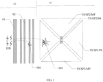
- FIG 1 is a plan view illustrating a display substrate provided by an embodiment of the present disclosure.
- a single ground line 01 i.e., GND line with a voltage of 0V
- the voltages of the ground lines are all 0V.
- FIG 1 A possible damaged region 001 is illustrated in FIG 1 .
- the region where the display region A1 is located is also a touch region.
- the touch structure TS includes a first sensor pattern SP1 and a second sensor pattern SP2, the first sensor pattern SP1 and the second sensor pattern SP2 are insulated from each other and intersected with each other, the first sensor pattern SP1 includes an integrally formed portion P0, and the second sensor pattern SP2 includes a plurality of main portions MP and a bridge line Bd connecting adjacent main portions MP.
- the main portions MP and the first sensor pattern SP1 can be formed by performing one single patterning process on a same film layer, and the bridge line Bd can be formed by performing another patterning process on another film layer.
- An insulating layer can be arranged between the bridge line Bd and the first sensor pattern SP1.
- FIG 2 is a schematic plan view illustrating a touch substrate provided by an embodiment of the present disclosure.
- the touch substrate 10 includes a touch structure TS, a first ground line 11, and at least one second ground line 12.
- the embodiment illustrated in FIG 2 is illustrated with reference to the case where one second ground line 12 is provided, by way of example, and in other embodiments, a plurality of second ground lines 12 can also be provided.
- the touch structure TS, the first ground line 11, and the second ground line 12 are located on a base substrate.
- the touch structure TS includes a sensor pattern SP and a touch line TL.
- the sensor pattern SP includes a first sensor pattern SP1 and a second sensor pattern SP2, and the first sensor pattern SP1 and the second sensor pattern SP2 are insulated from each other.
- the first sensor pattern SP1 and the second sensor pattern SP2 are intersected with each other.
- the first sensor pattern SP1 is perpendicular to the second sensor pattern SP2, but is not limited thereto.
- an extending direction of the first sensor pattern SP1 is intersected with an extending direction of the second sensor pattern SP2.
- the extending direction of the first sensor pattern SP1 is perpendicular to the extending direction of the second sensor pattern SP2, but is not limited thereto.
- an extending direction of an element may refer to the general trend or direction of the element, but is not limited thereto.
- the touch line TL includes a first touch line TL1 and a second touch line TL2.
- the first sensor pattern SP1 is connected with the first touch line TL1
- the second sensor pattern SP2 is connected with the second touch line TL2.
- some touch lines TL are schematically illustrated in FIG 2 .
- peripheral static electricity is firstly released by the second ground line, and static electricity that jumps over the second ground line is released by the first ground line, which can play a role of double protection, effectively reduce or avoid the influence of static electricity on the touch line and the sensor pattern, reduce the risk of touch failure caused by ESD, and achieve the purpose of improving the ability of preventing ESD, thereby avoiding the decline of product yield caused by ESD and achieving the purpose of improving product yield.
- the second ground line 12 and the first ground line 11 are electrically connected at a side of the touch structure TS, but not limited thereto.
- the second ground line 12 and the first ground line 11 are electrically connected at a side of the touch structure TS after the touch lines TL are gathered.
- the second ground line 12 and the first ground line 11 can also be electrically connected by a connection line at any other position.
- the first ground line 11 and the second ground line 12 are insulated from the touch structure TS, respectively. That is, the first ground line 11 is insulated from the touch structure TS, and the second ground line 12 is insulated from the touch structure TS.
- the first ground line 11 is located at a periphery of the touch structure TS.
- the at least one second ground line 12 is located at a side of the first ground line 11 facing away from the touch structure TS. That is, in a plane parallel with a surface of the base substrate, the second ground line 12 is located at a side of the first ground line 11 facing away from the touch control structure TS.
- the plane parallel with the surface of the base substrate is the surface of the base substrate for manufacturing various elements thereon.
- element A being located at a periphery of element B refers to that element A is located at the periphery of element B in a plan view.
- Element A and element B can have the same height with respect to the base substrate, that is, the distance from element A to the base substrate is equal to the distance from element B to the base substrate, but not limited thereto.
- the distance from element A to the base substrate may be unequal to the distance from element B to the base substrate.
- the embodiment illustrated in FIG 2 is illustrated with reference to the case where the first sensor pattern SP1 extends in the horizontal direction and the second sensor pattern SP2 extends in the vertical direction, by way of example, but is not limited thereto.
- the embodiment illustrated in FIG 2 is illustrated with reference to the case where the first sensor pattern SP1 is a receiving sensor (Rx) and the second sensor pattern SP2 is a transmitting sensor (Tx), by way of example, but is not limited thereto, and in other embodiments, they can be interchanged. That is, in some embodiments, the first sensor pattern SP1 is a transmitting sensor (Tx) and the second sensor pattern SP2 is a receiving sensor (Rx).
- a plurality of first sensor patterns SP1 and a plurality of second sensor patterns SP2 are illustrated in FIG 2 .
- the plurality of first sensor patterns SP1 are intersected with and insulated from the plurality of second sensor patterns SP2.
- One of the left and right ends of each first sensor pattern SP1 is connected with one first touch line TL1, or each first sensor pattern SP1 is connected with two first touch lines TL1 at the left and right ends of the first sensor pattern SP1.
- One of the upper and lower ends of each second sensor pattern SP2 is connected with one second touch line TL2, or each second sensor pattern SP2 is connected with two second touch lines TL2 at the upper and lower ends of the second sensor pattern SP2.
- each first sensor pattern SP1 is connected with one first touch line TL1 and each second sensor pattern SP2 is connected with two second touch lines TL2 at the upper and lower ends of the second sensor pattern SP2, by way of example.
- the touch substrate 10 further includes a flexible printed circuit 20, and both ends of the second ground line 12 are connected with different pins of the flexible printed circuit (FPC) 20.
- the second ground line 12 and the first ground line 11 are electrically connected at a position close to the FPC 20.
- the second ground line 12 and the first ground line 11 are electrically connected at a side of the touch structure TS close to the FPC 20.
- both ends of the second ground line 12 are electrically connected, at a side of the touch structure TS, with both ends of the first ground line 11, respectively.
- the first ground line 11 and the second ground line 12 can be led out to pads, respectively, and these pads are bonded to different pins of the flexible printed circuit 20, respectively.
- the second ground line 12 and the first ground line 11 are electrically connected at a side of the touch structure TS close to the pad of the touch line TL.
- FIG 2 illustrates that the FPC 20 includes a plurality of pins 201.
- different pins of the flexible printed circuit 20 can be insulated from each other so that signals can be transmitted separately.
- each pin 201 may correspond to a pad and be connected with the pad.
- one of the first sensor pattern SP1 and the second sensor pattern SP2 includes a main portion MP and a bridge line Bd, and the other of the first sensor pattern SP1 and the second sensor pattern SP2 includes an integrally formed portion P0.
- Two adjacent main portions MP in the plurality of main portions MP are connected through one bridge line Bd.
- adjacent main portions MP included in the same first sensor pattern SP1 are disposed at opposite sides of one second sensor pattern SP2, respectively.
- adjacent main portions MP included in the same first sensor pattern SP1 are disposed at the upper side and the lower side of one second sensor pattern SP2, respectively.
- a plurality of main portions MP and the integrally formed portions P0 can be located in the same layer and be formed by performing one single patterning process on the same film layer, and the bridge line Bd is located in another layer.
- FIG 2 is illustrated with reference to the case where the first sensor pattern SP1 is integrally formed and the second sensor pattern SP2 is formed in segments, by way of example. In other embodiments, it can be the case that the second sensor pattern SP2 is integrally formed and the first sensor pattern SP1 is formed in segments.
- a width of the second ground line 12 is equal to or greater than a width of the first ground line 11, but is not limited thereto. In other embodiments, the width of the second ground line 12 may be less than the width of the first ground line 11.
- the width of the first ground line 11 is in the range of 15-20 ⁇ m
- the width of the second ground line 12 is in the range of 15-20 ⁇ m
- the maximum distance between the first ground line 11 and the second ground line 12 is in the range of 20-50 ⁇ m
- the distance between the first ground line 11 and the touch line TL that is closest to the first ground line 11 is in the range of 10-40 ⁇ m.
- the width of the ground line or the touch line is the size thereof in the direction perpendicular to the extending direction thereof.
- the first ground line 11 is arranged around the touch structure TS, and the second ground line 12 is arranged around the first ground line 11.
- the second ground line 12 is arranged around the touch structure TS, and the first ground line 11 is arranged around the touch structure TS.
- the second ground line 12 is arranged around both the sensor pattern SP and the touch line TL, and the first ground line 11 is arranged around the sensor pattern SP and the touch line TL.
- the first ground line 11 and the second ground line 12 have an opening 30 at a side of the touch structure TS. As illustrated in FIG 2 , the opening 30 is located at the lower side of the touch structure TS.
- the touch substrate further includes a third ground line 13, and the third ground line 13 is located at the opening 30.
- the third ground line 13 is located within the opening 30.
- both ends of the third ground line 13 are connected with different pins of the flexible printed circuit (FPC) 20.
- the third ground line 13 is located between the first touch line TL1 and the second touch line TL2.
- the third ground line 13 is located between a pin of the FPC 20 connected with the first touch line TL1 and a pin of the FPC 20 connected with the second touch line TL2.
- At least one selected from the group consisting of the first ground line 11, the second ground line 12, and the touch line TL can be formed by two sub-lines which are connected and overlapped with each other in the direction perpendicular to the base substrate, that is, a design in which a line is formed of double-layer sub-lines can be adopted.
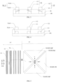
- FIG 3 is a cross-sectional view taken along line A-B in FIG 2 .
- FIG 4 is a cross-sectional view taken along line C-D in FIG 2 . The following description will be made with reference to FIG 2 , FIG 3, and FIG 4 .
- the second ground line 12 includes a first ground sub-line 121 and a second ground sub-line 122, an insulating layer IS is arranged between the first ground sub-line 121 and the second ground sub-line 122, and the first ground sub-line 121 and the second ground sub-line 122 are connected through a first via hole V1 penetrating the insulating layer IS.
- a plurality of first via holes V1 are distributed in the insulating layer IS, and the first ground sub-line 121 and the second ground sub-line 122 are connected at predetermined positions through the plurality of first via holes V1.
- FIG 3 is a cross-sectional view at a position where the first via hole is provided in the insulating layer IS
- FIG 4 is a cross-sectional view at a position where the first via hole is not provided in the insulating layer IS.
- an orthographic projection of the first ground sub-line 121 on the base substrate BS is at least partially overlapped with an orthographic projection of the second ground sub-line 122 on the base substrate BS.
- the orthographic projection of the first ground sub-line 121 on the base substrate BS coincides with the orthographic projection of the second ground sub-line 122 on the base substrate BS, but is not limited thereto.
- the first ground sub-line 121 is closer to the base substrate BS than the second ground sub-line 122.
- the first ground sub-line 121 is in contact with the second ground sub-line 122.
- the touch line TL (the second touch line TL2) includes a first touch sub-line TL01 and a second touch sub-line TL02
- the insulating layer IS is arranged between the first touch sub-line TL01 and the second touch sub-line TL02, and the first touch sub-line TL01 and the second touch sub-line TL02 are connected through a second via hole V2 penetrating the insulating layer IS.
- a plurality of second via holes V2 are distributed in the insulating layer IS, and the first touch sub-line TL01 and the second touch sub-line TL02 are connected at predetermined positions through the plurality of second via holes V2.
- FIG 3 is a cross-sectional view at a position where the second via hole is provided in the insulating layer IS
- FIG 4 is a cross-sectional view at a position where the second via hole is not provided in the insulating layer IS.
- the first touch line TL1 can also adopt the same structure as the second touch line TL2.
- the first touch sub-line TL01 is closer to the base substrate BS than the second touch sub-line TL02.
- an orthographic projection of the first touch sub-line TL01 on the base substrate BS is at least partially overlapped with an orthographic projection of the second touch sub-line TL02 on the base substrate BS.
- the orthographic projection of the first touch sub-line TL01 on the base substrate BS coincides with the orthographic projection of the second touch sub-line TL02 on the base substrate BS, but is not limited thereto.
- the first touch sub-line TL01 is in contact with the second touch sub-line TL02.
- the first ground line 11 includes a third ground sub-line 111 and a fourth ground sub-line 112, the insulating layer IS is arranged between the third ground sub-line 111 and the fourth ground sub-line 112, and the third ground sub-line 111 and the fourth ground sub-line 112 are connected through a third via hole V3 penetrating the insulating layer IS.
- a plurality of third via holes V3 are distributed in the insulating layer IS, and the third ground sub-line 111 and the fourth ground sub-line 112 are connected at predetermined positions through the plurality of third via holes V3. That is, the third ground sub-line 111 and the fourth ground sub-line 112 are connected in parallel.
- FIG 3 is a cross-sectional view at a position where the third via hole is provided in the insulating layer IS
- FIG 4 is a cross-sectional view at a position where the third via hole is not provided in the insulating layer IS.
- the third ground sub-line 111 is closer to the base substrate BS than the fourth ground sub-line 112.
- an orthographic projection of the third ground sub-line 111 on the base substrate BS is at least partially overlapped with an orthographic projection of the fourth ground sub-line 112 on the base substrate BS.
- the orthographic projection of the third ground sub-line 111 on the base substrate BS coincides with the orthographic projection of the fourth ground sub-line 112 on the base substrate BS, but is not limited thereto.
- the third ground sub-line 111 is in contact with the fourth ground sub-line 112.
- FIG 5 is a schematic diagram of the principle of double protection against ESD in a touch substrate provided by an embodiment of the present disclosure.
- FIG 5 is a schematic structural diagram of part of the touch substrate in FIG 2 .
- FIG 5 illustrates the touch line TL.
- At least one second ground line 12 is provided at a certain distance from the first ground line 11, and the peripheral static electricity is firstly released by the second ground line 12, and the static electricity that jumps over the second ground line 12 is released by the first ground line 11, thus playing a role of double protection on the touch line TL and the touch structure TS, reducing the risk of touch failure caused by ESD, achieving the purpose of improving the ability of preventing ESD, and further avoiding the decline of product yield caused by ESD and achieving the purpose of improving product yield.
- FIG 6 is a cross-sectional view taken along line E-F in FIG 5
- FIG 7 is a cross-sectional view taken along line G-H in FIG 5
- the integrally formed portion P0 is disposed in the same layer as the main portion MP.
- the integrally formed portion P0 and the main portion MP have a metal mesh structure, but are not limited thereto.
- two adjacent main portions MP are connected with the bridge line Bd through the fourth via hole V11 and the fifth via hole V12, respectively.
- one of the main portion MP and the bridge line Bd is in the same layer as the first ground sub-line 121, and the other of the main portion MP and the bridge line Bd is in the same layer as the second ground sub-line 122.
- the touch substrate provided by the embodiment of the present disclosure can be formed by the following method.
- the first conductive film and the second conductive film can be made of a metal material
- the integrally formed portions P0 and the main portions MP can be formed with a metal mesh structure
- the bridge lines Bd can be formed with a metal mesh structure
- other structures formed by patterning the first conductive film or the second conductive film may be formed with or may not be formed with a metal mesh structure.
- FIG 8 is a partial cross-sectional view illustrating a touch substrate provided by another embodiment of the present disclosure.
- the touch substrate includes a first ground line 11, a second ground line 12, and a plurality of touch lines TL
- the touch line TL includes a first touch sub-line TL01 and a second touch sub-line TL02
- the first touch sub-line TL01 and the second touch sub-line TL02 are connected through a second via hole V2 penetrating the insulating layer IS.
- FIG 8 illustrates four touch lines TL. The number of touch lines TL in the touch substrate can be determined as needed.
- a distance between the second ground line 12 that is closest to the first ground line 11 and the first ground line 11 is a first distance D1
- a distance between the touch line TL that is closest to the first ground line 11 and the first ground line 11 is a second distance D2
- the first distance D1 is less than the second distance D2.
- a distance D between adjacent touch lines TL is less than the second distance D2.
- the distance D between adjacent touch lines TL is less than the first distance D1, but is not limited thereto.
- the distance D between every two adjacent touch lines TL is equal, but not limited thereto.
- FIG 9 is a schematic plan view illustrating a touch substrate provided by another embodiment of the present disclosure.
- the touch substrate illustrated in FIG 9 is provided with a plurality of second ground lines 12, and the touch substrate illustrated in FIG 9 is illustrated with reference to the case where two second ground lines 12 are provided, by way of example.
- the plurality of second ground lines 12 can all be electrically connected with the first ground line 11.
- a distance between two adjacent second ground lines 12 is a third distance D3, and the third distance D3 is less than the first distance D1, so that both electro-static prevention and narrow frame design can be considered at the same time.
- the third distance D3 may be greater than or equal to the first distance D1.
- FIG 10 is a partial cross-sectional view illustrating a touch substrate provided by an embodiment of the present disclosure.
- the distance between adjacent second ground lines 12 is a third distance D3
- the third distance D3 is less than the first distance D1
- the third distance D3 is less than the second distance D2.
- At least one embodiment of the present disclosure further provides a touch display substrate, which includes any one of the above touch substrates.
- the touch display substrate includes a display region A1 and a peripheral region A2 located outside the display region A1, and the at least one second ground line 12 is located in the peripheral region A2.
- the region within the dashed box in FIG 2 is the display region A1, and the region other than the display region A1 is the peripheral region A2.
- the peripheral region A2 surrounds the display region A1.
- a display panel and a touch structure can be integrated. Therefore, flexible multiple layer on cell (FMLOC) touch technology came into being, and FMLOC touch technology is to directly manufacture various electrode layers and various lines of the touch structure on an encapsulation film, thus integrating the touch structure on the display panel. Therefore, the display device adopting FMLOC touch technology can not only realize the lighter and thinner design of the display device, but also realize touching based on flexible display.
- FMLOC flexible multiple layer on cell
- FIG 11 is a partial cross-sectional view illustrating a touch display substrate provided by an embodiment of the present disclosure.
- a base substrate 100 is disposed on a support substrate 200, and the base substrate 100 can be a flexible substrate, such as a Polyimide (PI) substrate, but not limited thereto.
- the material of the base substrate 100 can be selected as needed.
- the support substrate 200 can be a glass substrate. In some embodiments, the support substrate 200 can be removed.
- TFTs thin film transistors
- the thin film transistor 3123 can include a semiconductor layer, a gate electrode, a gate insulating layer, a source electrode, and a drain electrode, etc. As illustrated in FIG 11 , a buffer layer 111a, a semiconductor layer 112a, a gate insulating layer 113, a gate electrode 114, an interlayer dielectric layer 115, and a source-drain layer 116 are sequentially disposed on the base substrate 100, the source-drain layer 116 includes a source electrode 1161 and a drain electrode 1162, and the source electrode 1161 and the drain electrode 1162 are spaced apart from each other and can be connected with the semiconductor layer 112a through via holes, respectively.
- a planarization layer 117 can be disposed on the thin film transistor 3123, and a component to be encapsulated (OLED) 2123 can be disposed on the planarization layer 117.
- the component to be encapsulated (OLED) 2123 can include a first electrode 121a, a light-emitting functional layer 122a, and a second electrode 123, and the first electrode 121a can be electrically connected with the drain electrode 1162 through a via hole penetrating the planarization layer 117.
- a pixel defining layer 118 can be disposed on the first electrode 121a to facilitate the formation of the light-emitting functional layer 122a.
- the second electrode 123 can be electrically connected with an electrode lead 1163 through a connection electrode 1211.
- the light-emitting functional layer 122a can include a light-emitting layer, and can further include other functional layers, for example, can further include at least one selected from the group consisting of a hole injection layer, a hole transport layer, an electron transport layer, and an electron injection layer, etc., but is not limited thereto.
- the electrode lead 1163 can be formed in the same layer as the source-drain layer 116.
- the planarization layer 117 can be a resin layer.
- An encapsulation film 1123 can be formed on the component to be encapsulated (OLED) 2123.
- the encapsulation film 1123 covers the component to be encapsulated 2123 to prevent water and oxygen from invading the component to be encapsulated 2123.
- the structure of the component to be encapsulated (OLED) 2123 is not limited thererto.
- the base substrate 100 in FIG 11 can be the base substrate BS described above.
- the encapsulation film 1123 is disposed on the base substrate 100, the encapsulation film 1123 includes a first film 101, a second film 102, and a third film 103 that are sequentially away from the base substrate 100, the second film 102 is sandwiched between the first film 101 and the third film 103, and the first film 101 and the third film 103 are in contact with each other at an edge.
- the first film 101 and the third film 103 can be inorganic thin films, and for example, can be made of an inorganic oxide such as SiNx, SiOx, SiOxNy, SiCxNy, etc., but are not limited thereto.
- the second film 102 can be an organic thin film, and for example, can be made of an organic material such as resin, etc., but is not limited thereto.
- the resin can be, for example, a thermosetting resin, and the thermosetting resin includes, for example, an epoxy resin, but is not limited thereto.
- the resin can be, for example, a thermoplastic resin, the thermoplastic resin includes, for example, an acrylic (PMMA) resin, but is not limited thereto.
- the first film 101 and the third film 103 can be manufactured by chemical vapor deposition (CVD), and the second film 102 can be manufactured by ink jet printing (IJP).
- the first film 101 and the third film 103 can both serve as water-proof layers.
- the first film 101 can include a plurality of stacked sub-layers
- the second film 102 and the third film 103 can also include a plurality of stacked sub-layers, respectively.
- FIG 11 further illustrates a first dam 106 and a second dam 107.
- the first dam 106 can be formed in the same layer as the pixel defining layer 118.
- the second dam 107 can include a first sub-dam 1071 and a second sub-dam 1072.
- the first sub-dam 1071 can be formed in the same layer as the planarization layer 117
- the second sub-dam 1072 can be formed in the same layer as the pixel defining layer 118.
- the second film 102 is located between the first film 101 and the third film 103, and the first film 101 and the third film 103 are in contact with each other at an edge to form a contacting part 1031.
- FIG 11 also illustrates a display region A1 and a peripheral region A2.
- the touch structure TS is located in the display region A1
- the touch line TL is located in the peripheral region A2.
- an orthographic projection of the touch line TL on the base substrate 100 falls within an orthographic projection of the second film 102 on the base substrate 100.
- an orthographic projection of the first ground line 11 on the base substrate 100 falls within an orthographic projection of the second film 102 on the base substrate 100.
- an orthographic projection of the second ground line 12 on the base substrate 100 falls within the orthographic projection of the second film 102 on the base substrate 100.
- an orthographic projection of the plurality of second ground lines 12 on the base substrate 100 falls within the orthographic projection of the second film 102 on the base substrate 100.
- FIG 12 is a partial cross-sectional view illustrating a touch display substrate provided by another embodiment of the present disclosure.
- the touch display substrate illustrated in FIG 12 adjusts the arrangement positions of the first ground line 11 and the second ground line 12.
- the orthographic projection of the first ground line 11 on the base substrate 100 is located outside the orthographic projection of the second film 102 on the base substrate 100.
- the orthographic projection of the second ground line 12 on the base substrate 100 is located outside the orthographic projection of the second film 102 on the base substrate 100.
- the orthographic projection of the plurality of second grounding lines 12 on the base substrate 100 is located outside the orthographic projection of the second film 102 on the base substrate 100.
- the orthographic projection of the second ground line 12 on the base substrate 100 falls within the orthographic projection of the contacting part 1031 on the base substrate 100.
- the orthographic projection of the first ground line 11 on the base substrate 100 falls within the orthographic projection of the first dam 106 on the base substrate 100.
- the orthographic projection of the second ground line 12 on the base substrate 100 falls within the orthographic projection of the second dam 107 on the base substrate 100.
- At least one embodiment of the present disclosure further provides a touch display device, which includes any one of the above touch display substrates.
- the touch display device includes a flexible multi-layer on cell (FMLOC) product, but is not limited thereto.
- the touch display device can be a display device, such as a liquid crystal display, an electronic paper, an OLED (organic light-emitting diode) display, etc., and any product or component which includes the display device and has touch and display functions, such as a television, a digital camera, a mobile phone, a watch, a tablet computer, a notebook computer, and a navigator, etc.
- the above-mentioned distance can refer to spacing.
- the first distance D1, the second distance D2, the distance D, and the third distance D3 can refer to spacings, respectively.
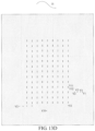
- At least one embodiment of the present disclosure further provides a manufacturing method of a touch substrate, as illustrated in FIGS. 13A-13F , which includes the following steps.
- Another embodiment of the present disclosure also provides a manufacturing method of a touch substrate, which can also refer to FIGS. 13A-13F , and includes the following steps.
- touch lines TL are not illustrated in FIGS. 13A-13F , and only seven touch lines TL are schematically illustrated in FIGS. 13A-13F .
- two touch lines TL are provided at the upper and lower sides of the second sensor pattern SP2, respectively, while only one touch line TL is provided at the left side of the first sensor pattern SP1.
- the number and shape of the first sensor patterns SP1 and the number and shape of the second sensor patterns SP2 are not limited to those illustrated in the figures, but can be determined as needed.
- the number of the second ground lines 12 is not limited to that illustrated in the figures.
- the insulating film ISF can be made of an insulating material, such as silicon oxide, silicon nitride, silicon oxynitride, or resin, etc., but is not limited thereto.
- the first conductive film L1 and the second conductive film L2 can be made of a metal material, but are not limited thereto.
- the elements arranged in the same layer are formed by performing one single patterning process on the same film layer.
- the elements arranged in the same layer are located on a surface of the same element facing away from the base substrate, but are not limited to this case.
- the elements arranged in the same layer can have different heights with respect to the base substrate.
- the patterning or patterning process can include only a photolithography process, or can include a photolithography process and an etching process, or can include other processes for forming a predetermined pattern such as printing, inkjet, etc.
- the photolithography process refers to a process including film formation, exposure, development, etc., which uses a photoresist, a mask, an exposure machine, etc., to form a pattern.
- a corresponding patterning process can be selected according to the structure to be formed in the embodiments of the present disclosure.
Landscapes
- Engineering & Computer Science (AREA)
- General Engineering & Computer Science (AREA)
- Theoretical Computer Science (AREA)
- Physics & Mathematics (AREA)
- General Physics & Mathematics (AREA)
- Human Computer Interaction (AREA)
- Computer Networks & Wireless Communication (AREA)
- Nonlinear Science (AREA)
- Mathematical Physics (AREA)
- Chemical & Material Sciences (AREA)
- Crystallography & Structural Chemistry (AREA)
- Optics & Photonics (AREA)
- Position Input By Displaying (AREA)
- Structure Of Printed Boards (AREA)
- Switches That Are Operated By Magnetic Or Electric Fields (AREA)
Abstract
Description
- The application claims priority of the
Chinese patent application No. 201911121001.0 filed on November 15, 2019 - At least one embodiment of the present disclosure relates to a touch substrate and a manufacturing method thereof, a touch display substrate and a touch display device.
- With the rapid development of active-matrix organic light-emitting diode (AMOLED), the development of touch display devices, such as mobile phones, has entered the era of full screen and narrow frame. In order to bring better use experience to users, display devices with the characteristics of full screen, narrow frame, high resolution, being rollable and wearable, being foldable, etc., will become an important development direction of AMOLED display devices in the future.
- At least one embodiment of the present disclosure relates to a touch substrate and a manufacturing method thereof, a touch display substrate, and a touch display device, which can play the role of double protection, effectively alleviate or avoid the influence of static electricity on the touch line and sensor pattern, reduce the risk of touch failure caused by ESD, and achieve the purpose of improving the ability of preventing ESD, thereby avoiding the decline of product yield caused by ESD and achieving the purpose of increasing product yield.
- At least one embodiment of the present disclosure provides a touch substrate, including: a touch structure, a first ground line, and at least one second ground line. The touch structure includes a sensor pattern and a touch line, the sensor pattern includes a plurality of first sensor patterns and a plurality of second sensor patterns, the plurality of first sensor patterns are intersected with and insulated from the plurality of second sensor patterns, and the touch line includes a plurality of first touch lines and a plurality of second touch lines, each of the plurality of first sensor patterns is connected with at least one of the first touch lines, and each of the plurality of second sensor patterns is connected with at least one of the second touch lines. The first ground line is located at a periphery of the touch structure. The at least one second ground line is located at a side of the first ground line facing away from the touch structure.
- In one or more embodiments of the present disclosure, the second ground line and the first ground line are electrically connected at a side of the touch structure.
- In one or more embodiments of the present disclosure, the first ground line is insulated from the touch structure, and the second ground line is insulated from the touch structure.
- In one or more embodiments of the present disclosure, a width of the second ground line is equal to or greater than a width of the first ground line.
- In one or more embodiments of the present disclosure, a maximum distance between the first ground line and the second ground line is in a range of 20-50 µm, and a distance between the first ground line and the touch line that is closest to the first ground line is in a range of 10-40 µm.
- In one or more embodiments of the present disclosure, a width of the first ground line is in a range of 15-20 µm, and a width of the second ground line is in a range of 15-20 µm.
- In one or more embodiments of the present disclosure, the first ground line is arranged around the touch structure, the second ground line is arranged around the first ground line, and the first ground line and the second ground line have a first interval.
- In one or more embodiments of the present disclosure, the touch structure, the first ground line, and the at least one second ground line are located on a base substrate, the second ground line includes a first ground sub-line and a second ground sub-line, the first ground sub-line is closer to the base substrate than the second ground sub-line, an insulating layer is arranged between the first ground sub-line and the second ground sub-line, the first ground sub-line and the second ground sub-line are connected through a first via hole penetrating the insulating layer, and an orthographic projection of the first ground sub-line on the base substrate is at least partially overlapped with an orthographic projection of the second ground sub-line on the base substrate.
- In one or more embodiments of the present disclosure, the touch substrate further includes a flexible printed circuit, both ends of the second ground line are connected with different pins of the flexible printed circuit.
- In one or more embodiments of the present disclosure, the touch substrate further includes a third ground line, the first ground line and the second ground line have an opening at a side of the touch structure, the third ground line is located within the opening, and both ends of the third ground line are connected with different pins of the flexible printed circuit.
- In one or more embodiments of the present disclosure, at least one of the first touch line and the second touch line includes a first touch sub-line and a second touch sub-line, the first touch sub-line is closer to the base substrate than the second touch sub-line, the insulating layer is arranged between the first touch sub-line and the second touch sub-line, the first touch sub-line and the second touch sub-line are connected through a second via hole penetrating the insulating layer, and an orthographic projection of the first touch sub-line on the base substrate is at least partially overlapped with an orthographic projection of the second touch sub-line on the base substrate.
- In one or more embodiments of the present disclosure, one of the first sensor pattern and the second sensor pattern includes a main portion and a bridge line, one of the main portion and the bridge line is in a same layer as the first ground sub-line, and the other of the main portion and the bridge line is in a same layer as the second ground sub-line.
- In one or more embodiments of the present disclosure, the other of the first sensor pattern and the second sensor pattern includes an integrally formed portion, and the integrally formed portion is in a same layer as the main portion.
- In one or more embodiments of the present disclosure, the first ground line includes a third ground sub-line and a fourth ground sub-line, the third ground sub-line is closer to the base substrate than the fourth ground sub-line, the insulating layer is arranged between the third ground sub-line and the fourth ground sub-line, the third ground sub-line and the fourth ground sub-line are connected through a third via hole penetrating the insulating layer, and an orthographic projection of the third ground sub-line on the base substrate is at least partially overlapped with an orthographic projection of the fourth ground sub-line on the base substrate.
- In one or more embodiments of the present disclosure, the bridge line, the first ground sub-line, the third ground sub-line, and the first touch sub-line are in a same layer, and the integrally formed portion, the main portion, the second ground sub-line, the fourth ground sub-line, and the second touch sub-line are in a same layer.
- In one or more embodiments of the present disclosure, at least one selected from the group consisting of the bridge line, the integrally formed portion, and the main portion has a metal mesh structure.
- In one or more embodiments of the present disclosure, a distance between the second ground line that is closest to the first ground line and the first ground line is less than a distance between the touch line that is closest to the first ground line and the first ground line.
- In one or more embodiments of the present disclosure, a plurality of second ground lines are provided, and a distance between two adjacent second ground lines is less than a distance between the second ground line that is closest to the first ground line and the first ground line.
- At least one embodiment of the present disclosure further provides a touch display substrate, including any one of the touch substrates described above.
- In one or more embodiments of the present disclosure, the touch display substrate includes a display region and a peripheral region located outside the display region, and the at least one second ground line is located in the peripheral region.
- In one or more embodiments of the present disclosure, the touch display substrate further includes a base substrate and an encapsulation film, the touch structure, the first ground line, and the at least one second ground line are located at a side of the encapsulation film facing away from the base substrate.
- In one or more embodiments of the present disclosure, the encapsulation film includes a first film, a second film, and a third film, the second film is located between the first film and the third film, and the first film and the third film are in contact with each other at an edge to form a contacting part; and an orthographic projection of the at least one second ground line on the base substrate falls within an orthographic projection of the second film on the base substrate.
- In one or more embodiments of the present disclosure, the encapsulation film includes a first film, a second film, and a third film, the second film is located between the first film and the third film, and the first film and the third film are in contact with each other at an edge to form a contacting part; and an orthographic projection of the at least one second ground line on the base substrate falls within an orthographic projection of the contacting part on the base substrate.
- At least one embodiment of the present disclosure further provides a touch display device, including any one of the touch display substrates described above.
- At least one embodiment of the present disclosure further provides a manufacturing method of a touch substrate, including: forming a first conductive film on a base substrate; patterning the first conductive film to form a first pattern, the first pattern including a bridge line, a first touch sub-line, a first ground sub-line, and a third ground sub-line; forming an insulating film; forming a first via hole, a second via hole, a third via hole, a fourth via hole, and a fifth via hole in the insulating film; forming a second conductive film; and patterning the second conductive film to form a second pattern, the second pattern including a second touch sub-line, a second ground sub-line, a fourth ground sub-line, an integrally formed portion, and a main portion, the first ground sub-line and the second ground sub-line are connected through the first via hole to form a second ground line, the first touch sub-line and the second touch sub-line are connected through the second via hole to form a touch line, the third ground sub-line and the fourth ground sub-line are connected through the third via hole to form a first ground line, and adjacent main portions are connected with the bridge line through the fourth via hole and the fifth via hole, respectively.
- In one or more embodiments of the present disclosure, the first pattern further includes a fifth ground sub-line, a sixth via hole is further formed in the insulating film, the second pattern further includes a sixth ground sub-line, and the fifth ground sub-line and the sixth ground sub-line are connected through the sixth via hole to form a third ground line.
- In order to clearly illustrate the technical solutions of the embodiments of the present disclosure, the drawings of the embodiments will be briefly described in the following; it is obvious that the described drawings are only related to some embodiments of the present disclosure and thus are not construed as any limitation to the present disclosure.
-
FIG 1 is a plan view illustrating a display substrate provided by an embodiment of the present disclosure; -
FIG 2 is a schematic plan view illustrating a touch substrate provided by an embodiment of the present disclosure; -
FIG 3 is a cross-sectional view taken along line A-B inFIG 2 ; -
FIG 4 is a cross-sectional view taken along line C-D inFIG 2 ; -
FIG 5 is a schematic diagram of the principle of double protection against ESD in a touch substrate provided by an embodiment of the present disclosure; -
FIG 6 is a cross-sectional view taken along line E-F inFIG 5 ; -
FIG 7 is a cross-sectional view taken along line G-H inFIG 5 ; -
FIG 8 is a partial cross-sectional view illustrating a touch substrate provided by another embodiment of the present disclosure; -
FIG 9 is a schematic plan view illustrating a touch substrate provided by another embodiment of the present disclosure; -
FIG 10 is a partial cross-sectional view illustrating a touch substrate provided by an embodiment of the present disclosure; -
FIG 11 is a partial cross-sectional view illustrating a touch display substrate provided by an embodiment of the present disclosure; -
FIG 12 is a partial cross-sectional view illustrating a touch display substrate provided by another embodiment of the present disclosure; and -
FIGS.13A-13F are flowcharts of a manufacturing method of a touch substrate provided by an embodiment of the present disclosure. - In order to make objectives, technical details, and advantages of the embodiments of the present disclosure more clear, the technical solutions of the embodiments will be described in a clearly and fully understandable way in connection with the drawings related to the embodiments of the present disclosure. It is obvious that the described embodiments are just a part but not all of the embodiments of the present disclosure. Based on the described embodiments herein, a person having ordinary skill in the art may obtain other embodiment(s), without any inventive work, which should be within the scope of the present disclosure.
- Unless otherwise defined, the technical terms or scientific terms used in the present disclosure have the same meanings as commonly understood by one of ordinary skill in the art to which the present disclosure belongs. The terms "first", "second", etc., which are used in the present disclosure, are not intended to indicate any sequence, amount, or importance, but distinguish various components. Also, the terms "comprises", "comprising", "includes", "including", etc., are intended to specify that the elements or the objects stated before these terms encompass the elements or the objects and equivalents thereof listed after these terms, but do not preclude the other elements or objects. The phrases "connect", "connected", etc., are not intended to define a physical connection or mechanical connection, but may include an electrical connection, directly or indirectly. "On," "under," "right," "left" and the like are only used to indicate relative position relationship, and when the position of the described object is changed, the relative position relationship may be changed accordingly.
- Touch technology such as flexible multi-layer on cell (FMLOC) touch technology was born in order to realize lighter weight, thinner thickness and narrower frame of touch display panel to adapt to foldable and rollable products. In touch display devices, static electricity easily leads to touch failure and causes touch defect. Static electricity includes, but is not limited to, static electricity generated during manufacture or use.
-
FIG 1 is a plan view illustrating a display substrate provided by an embodiment of the present disclosure. With regard to the panel design of FMLOC touch technology, in terms of preventing electro-static discharge (ESD), a single ground line 01 (i.e., GND line with a voltage of 0V) can be designed around the panel to achieve the purpose of releasing static electricity. In the embodiments of the present disclosure, the voltages of the ground lines are all 0V. - Although a single ground line can obstruct ESD to a certain extent, there is also the risk that static electricity jumps over the
ground line 01, enters thetrace line 02 in the peripheral region A2 or the touch structure (touch pattern) TS in the display region (active area) A1, thereby damaging thetrace line 02 or the touch structure TS, and resulting in touch failure, as illustrated inFIG 1 . A possible damagedregion 001 is illustrated inFIG 1 . The region where the display region A1 is located is also a touch region. - As illustrated in
FIG 1 , the touch structure TS includes a first sensor pattern SP1 and a second sensor pattern SP2, the first sensor pattern SP1 and the second sensor pattern SP2 are insulated from each other and intersected with each other, the first sensor pattern SP1 includes an integrally formed portion P0, and the second sensor pattern SP2 includes a plurality of main portions MP and a bridge line Bd connecting adjacent main portions MP. The main portions MP and the first sensor pattern SP1 can be formed by performing one single patterning process on a same film layer, and the bridge line Bd can be formed by performing another patterning process on another film layer. An insulating layer can be arranged between the bridge line Bd and the first sensor pattern SP1. -
FIG 2 is a schematic plan view illustrating a touch substrate provided by an embodiment of the present disclosure. As illustrated inFIG 2 , thetouch substrate 10 includes a touch structure TS, afirst ground line 11, and at least onesecond ground line 12. The embodiment illustrated inFIG 2 is illustrated with reference to the case where onesecond ground line 12 is provided, by way of example, and in other embodiments, a plurality ofsecond ground lines 12 can also be provided. The touch structure TS, thefirst ground line 11, and thesecond ground line 12 are located on a base substrate. - For example, as illustrated in
FIG 2 , the touch structure TS includes a sensor pattern SP and a touch line TL. The sensor pattern SP includes a first sensor pattern SP1 and a second sensor pattern SP2, and the first sensor pattern SP1 and the second sensor pattern SP2 are insulated from each other. The first sensor pattern SP1 and the second sensor pattern SP2 are intersected with each other. For example, the first sensor pattern SP1 is perpendicular to the second sensor pattern SP2, but is not limited thereto. For example, an extending direction of the first sensor pattern SP1 is intersected with an extending direction of the second sensor pattern SP2. For example, the extending direction of the first sensor pattern SP1 is perpendicular to the extending direction of the second sensor pattern SP2, but is not limited thereto. For example, an extending direction of an element may refer to the general trend or direction of the element, but is not limited thereto. For example, as illustrated inFIG 2 , the touch line TL includes a first touch line TL1 and a second touch line TL2. For example, as illustrated inFIG 2 , the first sensor pattern SP1 is connected with the first touch line TL1, and the second sensor pattern SP2 is connected with the second touch line TL2. For the sake of clarity, some touch lines TL are schematically illustrated inFIG 2 . - In the touch substrate provided by the embodiment of the present disclosure, by providing the second ground line, peripheral static electricity is firstly released by the second ground line, and static electricity that jumps over the second ground line is released by the first ground line, which can play a role of double protection, effectively reduce or avoid the influence of static electricity on the touch line and the sensor pattern, reduce the risk of touch failure caused by ESD, and achieve the purpose of improving the ability of preventing ESD, thereby avoiding the decline of product yield caused by ESD and achieving the purpose of improving product yield.
- For example, as illustrated in
FIG 2 , thesecond ground line 12 and thefirst ground line 11 are electrically connected at a side of the touch structure TS, but not limited thereto. For example, as illustrated inFIG 2 , thesecond ground line 12 and thefirst ground line 11 are electrically connected at a side of the touch structure TS after the touch lines TL are gathered. Of course, in the embodiment of the present disclosure, thesecond ground line 12 and thefirst ground line 11 can also be electrically connected by a connection line at any other position. For example, as illustrated inFIG 2 , thefirst ground line 11 and thesecond ground line 12 are insulated from the touch structure TS, respectively. That is, thefirst ground line 11 is insulated from the touch structure TS, and thesecond ground line 12 is insulated from the touch structure TS. - As illustrated in
FIG 2 , thefirst ground line 11 is located at a periphery of the touch structure TS. The at least onesecond ground line 12 is located at a side of thefirst ground line 11 facing away from the touch structure TS. That is, in a plane parallel with a surface of the base substrate, thesecond ground line 12 is located at a side of thefirst ground line 11 facing away from the touch control structure TS. For example, the plane parallel with the surface of the base substrate is the surface of the base substrate for manufacturing various elements thereon. In the embodiment of the present disclosure, element A being located at a periphery of element B refers to that element A is located at the periphery of element B in a plan view. Element A and element B can have the same height with respect to the base substrate, that is, the distance from element A to the base substrate is equal to the distance from element B to the base substrate, but not limited thereto. The distance from element A to the base substrate may be unequal to the distance from element B to the base substrate. - The embodiment illustrated in
FIG 2 is illustrated with reference to the case where the first sensor pattern SP1 extends in the horizontal direction and the second sensor pattern SP2 extends in the vertical direction, by way of example, but is not limited thereto. The embodiment illustrated inFIG 2 is illustrated with reference to the case where the first sensor pattern SP1 is a receiving sensor (Rx) and the second sensor pattern SP2 is a transmitting sensor (Tx), by way of example, but is not limited thereto, and in other embodiments, they can be interchanged. That is, in some embodiments, the first sensor pattern SP1 is a transmitting sensor (Tx) and the second sensor pattern SP2 is a receiving sensor (Rx). - A plurality of first sensor patterns SP1 and a plurality of second sensor patterns SP2 are illustrated in
FIG 2 . The plurality of first sensor patterns SP1 are intersected with and insulated from the plurality of second sensor patterns SP2. One of the left and right ends of each first sensor pattern SP1 is connected with one first touch line TL1, or each first sensor pattern SP1 is connected with two first touch lines TL1 at the left and right ends of the first sensor pattern SP1. One of the upper and lower ends of each second sensor pattern SP2 is connected with one second touch line TL2, or each second sensor pattern SP2 is connected with two second touch lines TL2 at the upper and lower ends of the second sensor pattern SP2. The embodiment illustrated inFIG 2 is illustrated with reference to the case where the left end of each first sensor pattern SP1 is connected with one first touch line TL1 and each second sensor pattern SP2 is connected with two second touch lines TL2 at the upper and lower ends of the second sensor pattern SP2, by way of example. - For example, as illustrated in
FIG 2 , thetouch substrate 10 further includes a flexible printedcircuit 20, and both ends of thesecond ground line 12 are connected with different pins of the flexible printed circuit (FPC) 20. For example, as illustrated inFIG 2 , thesecond ground line 12 and thefirst ground line 11 are electrically connected at a position close to theFPC 20. For example, as illustrated inFIG 2 , thesecond ground line 12 and thefirst ground line 11 are electrically connected at a side of the touch structure TS close to theFPC 20. For example, both ends of thesecond ground line 12 are electrically connected, at a side of the touch structure TS, with both ends of thefirst ground line 11, respectively. Thefirst ground line 11 and thesecond ground line 12 can be led out to pads, respectively, and these pads are bonded to different pins of the flexible printedcircuit 20, respectively. For example, thesecond ground line 12 and thefirst ground line 11 are electrically connected at a side of the touch structure TS close to the pad of the touch line TL.FIG 2 illustrates that theFPC 20 includes a plurality ofpins 201. For example, different pins of the flexible printedcircuit 20 can be insulated from each other so that signals can be transmitted separately. For example, eachpin 201 may correspond to a pad and be connected with the pad. - For example, as illustrated in
FIG 2 , one of the first sensor pattern SP1 and the second sensor pattern SP2 includes a main portion MP and a bridge line Bd, and the other of the first sensor pattern SP1 and the second sensor pattern SP2 includes an integrally formed portion P0. Two adjacent main portions MP in the plurality of main portions MP are connected through one bridge line Bd. For example, as illustrated inFIG 2 , adjacent main portions MP included in the same first sensor pattern SP1 are disposed at opposite sides of one second sensor pattern SP2, respectively. For example, as illustrated inFIG 2 , adjacent main portions MP included in the same first sensor pattern SP1 are disposed at the upper side and the lower side of one second sensor pattern SP2, respectively. A plurality of main portions MP and the integrally formed portions P0 can be located in the same layer and be formed by performing one single patterning process on the same film layer, and the bridge line Bd is located in another layer.FIG 2 is illustrated with reference to the case where the first sensor pattern SP1 is integrally formed and the second sensor pattern SP2 is formed in segments, by way of example. In other embodiments, it can be the case that the second sensor pattern SP2 is integrally formed and the first sensor pattern SP1 is formed in segments. - For example, in order to better play the role of electro-static protection, a width of the
second ground line 12 is equal to or greater than a width of thefirst ground line 11, but is not limited thereto. In other embodiments, the width of thesecond ground line 12 may be less than the width of thefirst ground line 11. - For example, the width of the
first ground line 11 is in the range of 15-20 µm, the width of thesecond ground line 12 is in the range of 15-20 µm, the maximum distance between thefirst ground line 11 and thesecond ground line 12 is in the range of 20-50 µm, and the distance between thefirst ground line 11 and the touch line TL that is closest to thefirst ground line 11 is in the range of 10-40 µm. In the embodiment of the present disclosure, the width of the ground line or the touch line is the size thereof in the direction perpendicular to the extending direction thereof. - For example, as illustrated in
FIG 2 , thefirst ground line 11 is arranged around the touch structure TS, and thesecond ground line 12 is arranged around thefirst ground line 11. For example, as illustrated inFIG 2 , thesecond ground line 12 is arranged around the touch structure TS, and thefirst ground line 11 is arranged around the touch structure TS. For example, thesecond ground line 12 is arranged around both the sensor pattern SP and the touch line TL, and thefirst ground line 11 is arranged around the sensor pattern SP and the touch line TL. For example, as illustrated inFIG 2 , thefirst ground line 11 and thesecond ground line 12 have anopening 30 at a side of the touch structure TS. As illustrated inFIG 2 , theopening 30 is located at the lower side of the touch structure TS. - For example, as illustrated in
FIG 2 , in order to further play the role of electro-static protection, the touch substrate further includes athird ground line 13, and thethird ground line 13 is located at theopening 30. For example, thethird ground line 13 is located within theopening 30. For example, both ends of thethird ground line 13 are connected with different pins of the flexible printed circuit (FPC) 20. For example, thethird ground line 13 is located between the first touch line TL1 and the second touch line TL2. For example, thethird ground line 13 is located between a pin of theFPC 20 connected with the first touch line TL1 and a pin of theFPC 20 connected with the second touch line TL2. - In some embodiments of the present disclosure, in order to reduce resistance of the line, at least one selected from the group consisting of the
first ground line 11, thesecond ground line 12, and the touch line TL can be formed by two sub-lines which are connected and overlapped with each other in the direction perpendicular to the base substrate, that is, a design in which a line is formed of double-layer sub-lines can be adopted. -
FIG 3 is a cross-sectional view taken along line A-B inFIG 2 .FIG 4 is a cross-sectional view taken along line C-D inFIG 2 . The following description will be made with reference toFIG 2 ,FIG 3, and FIG 4 . - For example, as illustrated in
FIG 3 and FIG 4 , in order to reduce resistance of the line, thesecond ground line 12 includes afirst ground sub-line 121 and asecond ground sub-line 122, an insulating layer IS is arranged between thefirst ground sub-line 121 and thesecond ground sub-line 122, and thefirst ground sub-line 121 and thesecond ground sub-line 122 are connected through a first via hole V1 penetrating the insulating layer IS. A plurality of first via holes V1 are distributed in the insulating layer IS, and thefirst ground sub-line 121 and thesecond ground sub-line 122 are connected at predetermined positions through the plurality of first via holes V1. That is, thefirst ground sub-line 121 and thesecond ground sub-line 122 are connected in parallel.FIG 3 is a cross-sectional view at a position where the first via hole is provided in the insulating layer IS, andFIG 4 is a cross-sectional view at a position where the first via hole is not provided in the insulating layer IS. - For example, as illustrated in
FIG 3 and FIG 4 , an orthographic projection of thefirst ground sub-line 121 on the base substrate BS is at least partially overlapped with an orthographic projection of thesecond ground sub-line 122 on the base substrate BS. In some embodiments, the orthographic projection of thefirst ground sub-line 121 on the base substrate BS coincides with the orthographic projection of thesecond ground sub-line 122 on the base substrate BS, but is not limited thereto. For example, as illustrated inFIG 4 , thefirst ground sub-line 121 is closer to the base substrate BS than thesecond ground sub-line 122. For example, as illustrated inFIG 4 , thefirst ground sub-line 121 is in contact with thesecond ground sub-line 122. - For example, in order to reduce resistance of the line, as illustrated in
FIG 3 and FIG 4 , the touch line TL (the second touch line TL2) includes a first touch sub-line TL01 and a second touch sub-line TL02, the insulating layer IS is arranged between the first touch sub-line TL01 and the second touch sub-line TL02, and the first touch sub-line TL01 and the second touch sub-line TL02 are connected through a second via hole V2 penetrating the insulating layer IS. A plurality of second via holes V2 are distributed in the insulating layer IS, and the first touch sub-line TL01 and the second touch sub-line TL02 are connected at predetermined positions through the plurality of second via holes V2. That is, the first touch sub-line TL01 and the second touch sub-line TL02 are connected in parallel.FIG 3 is a cross-sectional view at a position where the second via hole is provided in the insulating layer IS, andFIG 4 is a cross-sectional view at a position where the second via hole is not provided in the insulating layer IS. The first touch line TL1 can also adopt the same structure as the second touch line TL2. - For example, as illustrated in
FIG 3 and FIG 4 , the first touch sub-line TL01 is closer to the base substrate BS than the second touch sub-line TL02. For example, as illustrated inFIG 3 and FIG 4 , an orthographic projection of the first touch sub-line TL01 on the base substrate BS is at least partially overlapped with an orthographic projection of the second touch sub-line TL02 on the base substrate BS. In some embodiments, the orthographic projection of the first touch sub-line TL01 on the base substrate BS coincides with the orthographic projection of the second touch sub-line TL02 on the base substrate BS, but is not limited thereto. For example, as illustrated inFIG 4 , the first touch sub-line TL01 is in contact with the second touch sub-line TL02. - For example, as illustrated in
FIG 3 and FIG 4 , in order to reduce resistance of the line, thefirst ground line 11 includes athird ground sub-line 111 and afourth ground sub-line 112, the insulating layer IS is arranged between thethird ground sub-line 111 and thefourth ground sub-line 112, and thethird ground sub-line 111 and thefourth ground sub-line 112 are connected through a third via hole V3 penetrating the insulating layer IS. A plurality of third via holes V3 are distributed in the insulating layer IS, and thethird ground sub-line 111 and thefourth ground sub-line 112 are connected at predetermined positions through the plurality of third via holes V3. That is, thethird ground sub-line 111 and thefourth ground sub-line 112 are connected in parallel.FIG 3 is a cross-sectional view at a position where the third via hole is provided in the insulating layer IS, andFIG 4 is a cross-sectional view at a position where the third via hole is not provided in the insulating layer IS. - For example, as illustrated in
FIG 3 and FIG 4 , thethird ground sub-line 111 is closer to the base substrate BS than thefourth ground sub-line 112. For example, as illustrated inFIG 3 and FIG 4 , an orthographic projection of thethird ground sub-line 111 on the base substrate BS is at least partially overlapped with an orthographic projection of thefourth ground sub-line 112 on the base substrate BS. In some embodiments, the orthographic projection of thethird ground sub-line 111 on the base substrate BS coincides with the orthographic projection of thefourth ground sub-line 112 on the base substrate BS, but is not limited thereto. For example, as illustrated inFIG 4 , thethird ground sub-line 111 is in contact with thefourth ground sub-line 112. -
FIG 5 is a schematic diagram of the principle of double protection against ESD in a touch substrate provided by an embodiment of the present disclosure.FIG 5 is a schematic structural diagram of part of the touch substrate inFIG 2 .FIG 5 illustrates the touch line TL. - Referring to
FIG 2 andFIG 5 , in the touch substrate provided by the embodiment of the present disclosure, at least onesecond ground line 12 is provided at a certain distance from thefirst ground line 11, and the peripheral static electricity is firstly released by thesecond ground line 12, and the static electricity that jumps over thesecond ground line 12 is released by thefirst ground line 11, thus playing a role of double protection on the touch line TL and the touch structure TS, reducing the risk of touch failure caused by ESD, achieving the purpose of improving the ability of preventing ESD, and further avoiding the decline of product yield caused by ESD and achieving the purpose of improving product yield. -
FIG 6 is a cross-sectional view taken along line E-F inFIG 5 , andFIG 7 is a cross-sectional view taken along line G-H inFIG 5 . For example, as illustrated inFIG 6 , the integrally formed portion P0 is disposed in the same layer as the main portion MP. For example, the integrally formed portion P0 and the main portion MP have a metal mesh structure, but are not limited thereto. - For example, as illustrated in
FIG 5 andFIG 6 , two adjacent main portions MP are connected with the bridge line Bd through the fourth via hole V11 and the fifth via hole V12, respectively. - For example, in order to simplify the manufacturing process, one of the main portion MP and the bridge line Bd is in the same layer as the
first ground sub-line 121, and the other of the main portion MP and the bridge line Bd is in the same layer as thesecond ground sub-line 122. - For example, the touch substrate provided by the embodiment of the present disclosure can be formed by the following method.
- (1) Forming a first conductive film on a base substrate BS, and patterning the first conductive film to form a bridge line Bd, a first touch sub-line TL01, a
first ground sub-line 121, and athird ground sub-line 111. - (2) Forming an insulating film.
- (3) Forming a first via hole V1, a second via hole V2, a third via hole V3, a fourth via hole V11, and a fifth via hole V12 in the insulating film to form an insulating layer IS.
- (4) forming a second conductive film, patterning the second conductive film to form a second touch sub-line TL02, a
second ground sub-line 122, afourth ground sub-line 112, an integrally formed portion P0, and a main portion MP; thefirst ground sub-line 121 and thesecond ground sub-line 122 are connected through the first via hole V1, the first touch sub-line TL01 and the second touch sub-line TL02 are connected through the second via hole V2, thethird ground sub-line 111 and thefourth ground sub-line 112 are connected through the third via V3, and adjacent main portions MP are connected with the bridge line Bd through the fourth via hole V11 and the fifth via hole V12, respectively. - For example, the first conductive film and the second conductive film can be made of a metal material, the integrally formed portions P0 and the main portions MP can be formed with a metal mesh structure, the bridge lines Bd can be formed with a metal mesh structure, and other structures formed by patterning the first conductive film or the second conductive film may be formed with or may not be formed with a metal mesh structure.
-
FIG 8 is a partial cross-sectional view illustrating a touch substrate provided by another embodiment of the present disclosure. As illustrated inFIG 8 , the touch substrate includes afirst ground line 11, asecond ground line 12, and a plurality of touch lines TL, the touch line TL includes a first touch sub-line TL01 and a second touch sub-line TL02, and the first touch sub-line TL01 and the second touch sub-line TL02 are connected through a second via hole V2 penetrating the insulating layer IS.FIG 8 illustrates four touch lines TL. The number of touch lines TL in the touch substrate can be determined as needed. - Referring to
FIG 2 andFIG 8 , a distance between thesecond ground line 12 that is closest to thefirst ground line 11 and thefirst ground line 11 is a first distance D1, a distance between the touch line TL that is closest to thefirst ground line 11 and thefirst ground line 11 is a second distance D2, and in order to improve the electro-static protection effect, the first distance D1 is less than the second distance D2. - For example, in order to improve the electro-static protection effect, as illustrated in
FIG 8 , a distance D between adjacent touch lines TL is less than the second distance D2. For example, as illustrated inFIG 8 , the distance D between adjacent touch lines TL is less than the first distance D1, but is not limited thereto. For example, the distance D between every two adjacent touch lines TL is equal, but not limited thereto. -
FIG 9 is a schematic plan view illustrating a touch substrate provided by another embodiment of the present disclosure. Compared with the touch substrate illustrated inFIG 2 , the touch substrate illustrated inFIG 9 is provided with a plurality of second ground lines 12, and the touch substrate illustrated inFIG 9 is illustrated with reference to the case where twosecond ground lines 12 are provided, by way of example. The plurality ofsecond ground lines 12 can all be electrically connected with thefirst ground line 11. A distance between two adjacent second ground lines 12 is a third distance D3, and the third distance D3 is less than the first distance D1, so that both electro-static prevention and narrow frame design can be considered at the same time. Of course, in other embodiments, the third distance D3 may be greater than or equal to the first distance D1. -
FIG 10 is a partial cross-sectional view illustrating a touch substrate provided by an embodiment of the present disclosure. Referring toFIG 8 andFIG 10 , the distance between adjacent second ground lines 12 is a third distance D3, the third distance D3 is less than the first distance D1, and the third distance D3 is less than the second distance D2. - At least one embodiment of the present disclosure further provides a touch display substrate, which includes any one of the above touch substrates.
- For example, as illustrated in
FIG 2 , the touch display substrate includes a display region A1 and a peripheral region A2 located outside the display region A1, and the at least onesecond ground line 12 is located in the peripheral region A2. The region within the dashed box inFIG 2 is the display region A1, and the region other than the display region A1 is the peripheral region A2. The peripheral region A2 surrounds the display region A1. - In order to realize the lighter and thinner design of a display device (e.g., an organic light emitting diode display device), a display panel and a touch structure can be integrated. Therefore, flexible multiple layer on cell (FMLOC) touch technology came into being, and FMLOC touch technology is to directly manufacture various electrode layers and various lines of the touch structure on an encapsulation film, thus integrating the touch structure on the display panel. Therefore, the display device adopting FMLOC touch technology can not only realize the lighter and thinner design of the display device, but also realize touching based on flexible display.
-
FIG 11 is a partial cross-sectional view illustrating a touch display substrate provided by an embodiment of the present disclosure. In an embodiment, as illustrated inFIG 11 , abase substrate 100 is disposed on asupport substrate 200, and thebase substrate 100 can be a flexible substrate, such as a Polyimide (PI) substrate, but not limited thereto. The material of thebase substrate 100 can be selected as needed. Thesupport substrate 200 can be a glass substrate. In some embodiments, thesupport substrate 200 can be removed. On thebase substrate 100, an array of thin film transistors (TFTs) 3123 can be disposed, and only onethin film transistor 3123 is illustrated inFIG 11 . Thethin film transistor 3123 can include a semiconductor layer, a gate electrode, a gate insulating layer, a source electrode, and a drain electrode, etc. As illustrated inFIG 11 , abuffer layer 111a, asemiconductor layer 112a, agate insulating layer 113, agate electrode 114, aninterlayer dielectric layer 115, and a source-drain layer 116 are sequentially disposed on thebase substrate 100, the source-drain layer 116 includes a source electrode 1161 and a drain electrode 1162, and the source electrode 1161 and the drain electrode 1162 are spaced apart from each other and can be connected with thesemiconductor layer 112a through via holes, respectively. Aplanarization layer 117 can be disposed on thethin film transistor 3123, and a component to be encapsulated (OLED) 2123 can be disposed on theplanarization layer 117. The component to be encapsulated (OLED) 2123 can include afirst electrode 121a, a light-emittingfunctional layer 122a, and asecond electrode 123, and thefirst electrode 121a can be electrically connected with the drain electrode 1162 through a via hole penetrating theplanarization layer 117. Apixel defining layer 118 can be disposed on thefirst electrode 121a to facilitate the formation of the light-emittingfunctional layer 122a. Thesecond electrode 123 can be electrically connected with anelectrode lead 1163 through aconnection electrode 1211. The light-emittingfunctional layer 122a can include a light-emitting layer, and can further include other functional layers, for example, can further include at least one selected from the group consisting of a hole injection layer, a hole transport layer, an electron transport layer, and an electron injection layer, etc., but is not limited thereto. For example, theelectrode lead 1163 can be formed in the same layer as the source-drain layer 116. Theplanarization layer 117 can be a resin layer. Anencapsulation film 1123 can be formed on the component to be encapsulated (OLED) 2123. Theencapsulation film 1123 covers the component to be encapsulated 2123 to prevent water and oxygen from invading the component to be encapsulated 2123. The structure of the component to be encapsulated (OLED) 2123 is not limited thererto. Thebase substrate 100 inFIG 11 can be the base substrate BS described above. - As illustrated in
FIG 11 , theencapsulation film 1123 is disposed on thebase substrate 100, theencapsulation film 1123 includes afirst film 101, asecond film 102, and athird film 103 that are sequentially away from thebase substrate 100, thesecond film 102 is sandwiched between thefirst film 101 and thethird film 103, and thefirst film 101 and thethird film 103 are in contact with each other at an edge. For example, thefirst film 101 and thethird film 103 can be inorganic thin films, and for example, can be made of an inorganic oxide such as SiNx, SiOx, SiOxNy, SiCxNy, etc., but are not limited thereto. For example, thesecond film 102 can be an organic thin film, and for example, can be made of an organic material such as resin, etc., but is not limited thereto. The resin can be, for example, a thermosetting resin, and the thermosetting resin includes, for example, an epoxy resin, but is not limited thereto. The resin can be, for example, a thermoplastic resin, the thermoplastic resin includes, for example, an acrylic (PMMA) resin, but is not limited thereto. For example, thefirst film 101 and thethird film 103 can be manufactured by chemical vapor deposition (CVD), and thesecond film 102 can be manufactured by ink jet printing (IJP). Thefirst film 101 and thethird film 103 can both serve as water-proof layers. For example, thefirst film 101 can include a plurality of stacked sub-layers, and thesecond film 102 and thethird film 103 can also include a plurality of stacked sub-layers, respectively. -
FIG 11 further illustrates afirst dam 106 and asecond dam 107. Thefirst dam 106 can be formed in the same layer as thepixel defining layer 118. Thesecond dam 107 can include a first sub-dam 1071 and asecond sub-dam 1072. For example, the first sub-dam 1071 can be formed in the same layer as theplanarization layer 117, and the second sub-dam 1072 can be formed in the same layer as thepixel defining layer 118. - As illustrated in
FIG 11 , thesecond film 102 is located between thefirst film 101 and thethird film 103, and thefirst film 101 and thethird film 103 are in contact with each other at an edge to form a contactingpart 1031. -
FIG 11 also illustrates a display region A1 and a peripheral region A2. As illustrated inFIG 11 , the touch structure TS is located in the display region A1, and the touch line TL is located in the peripheral region A2. As illustrated inFIG 11 , an orthographic projection of the touch line TL on thebase substrate 100 falls within an orthographic projection of thesecond film 102 on thebase substrate 100. - In the touch display substrate illustrated in
FIG 11 , an orthographic projection of thefirst ground line 11 on thebase substrate 100 falls within an orthographic projection of thesecond film 102 on thebase substrate 100. For example, as illustrated inFIG 11 , an orthographic projection of thesecond ground line 12 on thebase substrate 100 falls within the orthographic projection of thesecond film 102 on thebase substrate 100. In the case where a plurality ofsecond ground lines 12 are provided, an orthographic projection of the plurality of second ground lines 12 on thebase substrate 100 falls within the orthographic projection of thesecond film 102 on thebase substrate 100. -
FIG 12 is a partial cross-sectional view illustrating a touch display substrate provided by another embodiment of the present disclosure. Compared with the touch display substrate illustrated inFIG 11 , the touch display substrate illustrated inFIG 12 adjusts the arrangement positions of thefirst ground line 11 and thesecond ground line 12. In the touch display substrate illustrated inFIG 12 , the orthographic projection of thefirst ground line 11 on thebase substrate 100 is located outside the orthographic projection of thesecond film 102 on thebase substrate 100. For example, as illustrated inFIG 12 , the orthographic projection of thesecond ground line 12 on thebase substrate 100 is located outside the orthographic projection of thesecond film 102 on thebase substrate 100. In the case where a plurality ofsecond ground lines 12 are provided, the orthographic projection of the plurality ofsecond grounding lines 12 on thebase substrate 100 is located outside the orthographic projection of thesecond film 102 on thebase substrate 100. - For example, as illustrated in
FIG 12 , the orthographic projection of thesecond ground line 12 on thebase substrate 100 falls within the orthographic projection of the contactingpart 1031 on thebase substrate 100. - For further example, as illustrated in
FIG 12 , the orthographic projection of thefirst ground line 11 on thebase substrate 100 falls within the orthographic projection of thefirst dam 106 on thebase substrate 100. For example, as illustrated inFIG 12 , the orthographic projection of thesecond ground line 12 on thebase substrate 100 falls within the orthographic projection of thesecond dam 107 on thebase substrate 100. - At least one embodiment of the present disclosure further provides a touch display device, which includes any one of the above touch display substrates.
- In the embodiment of the present disclosure, the touch display device includes a flexible multi-layer on cell (FMLOC) product, but is not limited thereto. The touch display device can be a display device, such as a liquid crystal display, an electronic paper, an OLED (organic light-emitting diode) display, etc., and any product or component which includes the display device and has touch and display functions, such as a television, a digital camera, a mobile phone, a watch, a tablet computer, a notebook computer, and a navigator, etc.
- For example, in the embodiment of the present disclosure, the above-mentioned distance can refer to spacing. For example, the first distance D1, the second distance D2, the distance D, and the third distance D3 can refer to spacings, respectively.
- At least one embodiment of the present disclosure further provides a manufacturing method of a touch substrate, as illustrated in
FIGS. 13A-13F , which includes the following steps. - (1) As illustrated in
FIG 13A , forming a first conductive film L1 on a base substrate. - (2) As illustrated in
FIG 13B , patterning the first conductive film L1 to form a first pattern P1, the first pattern P1 includes a bridge line Bd, a first touch sub-line TL01, afirst ground sub-line 121, athird ground sub-line 111, and afifth ground sub-line 131. - (3) As illustrated in
FIG 13C , forming an insulating film ISF. - (4) As illustrated in
FIG 13D , forming a first via hole V1, a second via hole V2, a third via hole V3, a fourth via hole V11, a fifth via hole V12, and a sixth via hole V31 in the insulating film ISF. - (5) As illustrated in
FIG 13E , forming a second conductive film L2. - (6) As illustrated in
FIG 13F , patterning the second conductive film L2 to form a second pattern p2; the second pattern P2 includes a second touch sub-line TL02, asecond ground sub-line 122, afourth ground sub-line 112, an integrally formed portion P0, a main portion MP, and asixth ground sub-line 132; thefirst ground sub-line 121 and thesecond ground sub-line 122 are connected through the first via hole V1 to form asecond ground line 12, the first touch sub-line TL01 and the second touch sub-line TL02 are connected through the second via hole V2 to form a touch line TL, thethird ground sub-line 111 and thefourth ground sub-line 112 are connected through the third via hole V3 to form afirst ground line 11, and adjacent main portions MP are connected with the bridge line Bd through the fourth via hole V11 and the fifth via hole V12, respectively, so as to form a second sensor pattern SP2; the integrally formed portion P0 is a first sensor pattern SP1; and thefifth ground sub-line 131 and thesixth ground sub-line 132 are connected through the sixth via hole V31 to form athird ground line 13. - (7) Bonding an
FPC 20 to the touch substrate by way of pressure welding. - The above description takes the formation of the touch substrate illustrated in
FIG 9 as an example. In the case where thethird ground line 13 is not provided, the steps of forming thefifth ground sub-line 131, thesixth ground sub-line 132, and the sixth via hole V31 are correspondingly removed. The method is described below. - Another embodiment of the present disclosure also provides a manufacturing method of a touch substrate, which can also refer to
FIGS. 13A-13F , and includes the following steps. - (1) As illustrated in
FIG 13A , forming a first conductive film L1 on a base substrate. - (2) As illustrated in
FIG 13B , patterning the first conductive film L1 to form a first pattern P1; the first pattern P1 includes a bridge line Bd, a first touch sub-line TL01, afirst ground sub-line 121, and athird ground sub-line 111. - (3) As illustrated in
FIG 13C , forming an insulating film ISF. - (4) As illustrated in
FIG 13D , forming a first via hole V1, a second via hole V2, a third via hole V3, a fourth via hole V11, and a fifth via hole V12 in the insulating film ISF, so as to form an insulating layer IS. - (5) As illustrated in
FIG 13E , forming a second conductive film L2. - (6) As illustrated in
FIG 13F , patterning the second conductive film L2 to form a second pattern p2; the second pattern P2 includes a second touch sub-line TL02, asecond ground sub-line 122, afourth ground sub-line 112, an integrally formed portion P0, and a main portion MP; thefirst ground sub-line 121 and thesecond ground sub-line 122 are connected through the first via hole V1 to form asecond ground line 12, the first touch sub-line TL01 and the second touch sub-line TL02 are connected through the second via hole V2 to form a touch line TL, thethird ground sub-line 111 and thefourth ground sub-line 112 are connected through the third via hole V3 to form afirst ground line 11, and adjacent main portions MP are connected with the bridge line Bd through the fourth via hole V11 and the fifth via hole V12, respectively, so as to form a second sensor pattern SP2; and the integrally formed portion P0 is a first sensor pattern SP1. - (7) Bonding an
FPC 20 to the touch substrate by way of pressure welding. - For the sake of clarity, all touch lines TL are not illustrated in
FIGS. 13A-13F , and only seven touch lines TL are schematically illustrated inFIGS. 13A-13F . In the embodiment of the present disclosure, two touch lines TL are provided at the upper and lower sides of the second sensor pattern SP2, respectively, while only one touch line TL is provided at the left side of the first sensor pattern SP1. - Of course, the number and shape of the first sensor patterns SP1 and the number and shape of the second sensor patterns SP2 are not limited to those illustrated in the figures, but can be determined as needed. And the number of the second ground lines 12 is not limited to that illustrated in the figures.
- For example, the insulating film ISF can be made of an insulating material, such as silicon oxide, silicon nitride, silicon oxynitride, or resin, etc., but is not limited thereto.
- For example, the first conductive film L1 and the second conductive film L2 can be made of a metal material, but are not limited thereto.
- It should be noted that, for the sake of clarity, the thickness of a layer or region is enlarged in the drawings for describing the embodiments of the present disclosure. It should be understood that in the case where an element such as a layer, film, region or substrate is referred to as being "on" or "under" another element, the element may be "directly" "on" or "under" the another element, or an intervening element may be present therebetween.
- In the embodiments of the present disclosure, the elements arranged in the same layer are formed by performing one single patterning process on the same film layer. For example, the elements arranged in the same layer are located on a surface of the same element facing away from the base substrate, but are not limited to this case. The elements arranged in the same layer can have different heights with respect to the base substrate.
- In the embodiments of the present disclosure, the patterning or patterning process can include only a photolithography process, or can include a photolithography process and an etching process, or can include other processes for forming a predetermined pattern such as printing, inkjet, etc. The photolithography process refers to a process including film formation, exposure, development, etc., which uses a photoresist, a mask, an exposure machine, etc., to form a pattern. A corresponding patterning process can be selected according to the structure to be formed in the embodiments of the present disclosure.
- In case of no conflict, features in one embodiment or in different embodiments can be combined.
- What have been described above are only specific implementations of the present disclosure, the protection scope of the present disclosure is not limited thereto. Any changes or substitutions easily occur to those skilled in the art within the technical scope of the present disclosure should be covered in the protection scope of the present disclosure. Therefore, the protection scope of the present disclosure should be based on the protection scope of the claims.
Claims (15)
- A touch substrate, comprising:a touch structure, comprising a sensor pattern and a touch line, wherein the sensor pattern comprises a plurality of first sensor patterns and a plurality of second sensor patterns, the plurality of first sensor patterns are intersected with and insulated from the plurality of second sensor patterns, and the touch line comprises a plurality of first touch lines and a plurality of second touch lines, each of the plurality of first sensor patterns is connected with at least one of the first touch lines, and each of the plurality of second sensor patterns is connected with at least one of the second touch lines;a first ground line, located at a periphery of the touch structure; andat least one second ground line, located at a side of the first ground line facing away from the touch structure,wherein the first ground line and the at least one second ground line are connected at a side of the touch structure and are connected with one ground connection line.
- The touch substrate according to claim 1, further comprising a flexible printed circuit, wherein one end of the ground connection line is connected with the flexible printed circuit.
- The touch substrate according to claim 1 or 2, wherein the at least one second ground line comprises a third ground line and a fourth ground line, the fourth ground line is located at a side of the third ground line facing away from the touch structure, and the third ground line and the fourth ground line are connected with the ground connection line,
- The touch substrate according to claim 3, wherein the first ground line and the third ground line have a first connection point, the ground connection line has a first endpoint, and the first connection point coincides with the first endpoint.
- The touch substrate according to claim 4, wherein the first ground line and the third ground line are connected with the ground connection line at the first connection point.
- The touch substrate according to claim 4 or 5, wherein the first ground line and the fourth ground line have a second connection point, and the second connection point is located at the ground connection line,preferably, the first ground line and the fourth ground line are connected with the ground connection line at the second connection point,further preferably, a minimum distance between the first connection point and the second connection point is greater than zero.
- The touch substrate according to any one of claims 1-6, wherein a width of the first ground line is the same as a width of the ground connection line, the width of the first ground line is a size of the first ground line in a direction perpendicular to an extending direction of the first ground line and in a plane parallel with a base substrate, and the width of the ground connection line is a size of the ground connection line in a direction perpendicular to an extending direction of the ground connection line and in the plane parallel with the base substrate,preferably, a width of the first ground line is greater than a width of the ground connection line, the width of the first ground line is a size of the first ground line in a direction perpendicular to an extending direction of the first ground line and in a plane parallel with the base substrate, and the width of the ground connection line is a size of the ground connection line in a direction perpendicular to an extending direction of the ground connection line and in a plane parallel with the base substrate,further preferably, a width of one of the at least one second ground line is greater than a width of the ground connection line, the width of the second ground line is a size of the second ground line in a direction perpendicular to an extending direction of the second ground line and in a plane parallel with the base substrate, and the width of the ground connection line is a size of the ground connection line in a direction perpendicular to an extending direction of the ground connection line and in a plane parallel with the base substrate.
- The touch substrate according to any one of claims 4-6, wherein two first connection points are provided, the touch substrate has a first center line, the two first connection points are located at two sides of the first center line, respectively, the first center line extends in a direction the same as an extending direction of the second sensor pattern,
preferably, the touch substrate further comprises a second center line, wherein the second center line is intersected with the first center line, the two first connection points are located at the same side of the second center line. - The touch substrate according to any one of claims 1-8, wherein the first ground line is insulated from the touch structure, and the second ground line is insulated from the touch structure,preferably, a maximum distance between the first ground line and the second ground line is in a range of 20-50 µm, and a distance between the first ground line and the touch line that is closest to the first ground line is in a range of 10-40 µm,further preferably, a width of the first ground line is in a range of 15-20 µm, and a width of one of the at least one second ground line is in a range of 15-20 µm.
- The touch substrate according to any one of claims 1-9, wherein the first ground line is arranged around the touch structure, the second ground line is arranged around the first ground line, and the first ground line and the second ground line have a first interval.
- The touch substrate according to any one of claims 1-10, wherein the second ground line comprises a first ground sub-line and a second ground sub-line, an insulating layer is arranged between the first ground sub-line and the second ground sub-line, the first ground sub-line and the second ground sub-line are connected through a first via hole penetrating the insulating layer.
- The touch substrate according to claim 11, wherein at least one of the first touch line and the second touch line comprises a first touch sub-line and a second touch sub-line, the insulating layer is arranged between the first touch sub-line and the second touch sub-line, the first touch sub-line and the second touch sub-line are connected through a second via hole penetrating the insulating layer.
- The touch substrate according to claim 12, wherein one of the first sensor pattern and the second sensor pattern comprises an integrally formed portion, and the other of the first sensor pattern and the second sensor pattern comprises a main portion and a bridge line, one of the main portion and the bridge line is in a same layer as the first ground sub-line, and the other of the main portion and the bridge line is in a same layer as the second ground sub-line,wherein the first ground line comprises a third ground sub-line and a fourth ground sub-line, the insulating layer is arranged between the third ground sub-line and the fourth ground sub-line, the third ground sub-line and the fourth ground sub-line are connected through a third via hole penetrating the insulating layer,preferably, the bridge line, the first ground sub-line, the third ground sub-line, and the first touch sub-line are in a same layer, and the integrally formed portion, the main portion, the second ground sub-line, the fourth ground sub-line, and the second touch sub-line are in a same layer,further preferably, at least one selected from the group consisting of the bridge line, the integrally formed portion, and the main portion has a metal mesh structure.
- The touch substrate according to any one of claims 1-13, further comprising a flexible printed circuit, wherein two ground connection lines are provided, the two ground connection lines are connected with different pins of the flexible printed circuit.
- A touch display substrate, comprising the touch substrate according to any one of claims 1-14.
Applications Claiming Priority (3)
| Application Number | Priority Date | Filing Date | Title |
|---|---|---|---|
| CN201911121001.0A CN112817469A (en) | 2019-11-15 | 2019-11-15 | Touch substrate and manufacturing method thereof, touch display substrate and touch display device |
| EP20886920.6A EP4060464B1 (en) | 2019-11-15 | 2020-09-14 | Touch substrate and manufacturing method therefor, touch display substrate, and touch display device |
| PCT/CN2020/115077 WO2021093443A1 (en) | 2019-11-15 | 2020-09-14 | Touch substrate and manufacturing method therefor, touch display substrate, and touch display device |
Related Parent Applications (2)
| Application Number | Title | Priority Date | Filing Date |
|---|---|---|---|
| EP20886920.6A Division EP4060464B1 (en) | 2019-11-15 | 2020-09-14 | Touch substrate and manufacturing method therefor, touch display substrate, and touch display device |
| EP20886920.6A Division-Into EP4060464B1 (en) | 2019-11-15 | 2020-09-14 | Touch substrate and manufacturing method therefor, touch display substrate, and touch display device |
Publications (3)
| Publication Number | Publication Date |
|---|---|
| EP4220361A2 true EP4220361A2 (en) | 2023-08-02 |
| EP4220361A3 EP4220361A3 (en) | 2023-09-13 |
| EP4220361B1 EP4220361B1 (en) | 2025-05-14 |
Family
ID=75851999
Family Applications (2)
| Application Number | Title | Priority Date | Filing Date |
|---|---|---|---|
| EP20886920.6A Active EP4060464B1 (en) | 2019-11-15 | 2020-09-14 | Touch substrate and manufacturing method therefor, touch display substrate, and touch display device |
| EP23162922.1A Active EP4220361B1 (en) | 2019-11-15 | 2020-09-14 | Touch substrate and manufacturing method therefor, touch display substrate, and touch display device |
Family Applications Before (1)
| Application Number | Title | Priority Date | Filing Date |
|---|---|---|---|
| EP20886920.6A Active EP4060464B1 (en) | 2019-11-15 | 2020-09-14 | Touch substrate and manufacturing method therefor, touch display substrate, and touch display device |
Country Status (5)
| Country | Link |
|---|---|
| US (2) | US11537253B2 (en) |
| EP (2) | EP4060464B1 (en) |
| KR (1) | KR102880797B1 (en) |
| CN (2) | CN112817469A (en) |
| WO (1) | WO2021093443A1 (en) |
Families Citing this family (15)
| Publication number | Priority date | Publication date | Assignee | Title |
|---|---|---|---|---|
| KR102954038B1 (en) * | 2020-08-21 | 2026-04-17 | 삼성디스플레이 주식회사 | Display device |
| KR102960989B1 (en) * | 2020-10-22 | 2026-05-06 | 삼성디스플레이 주식회사 | Display device |
| KR102860946B1 (en) * | 2020-11-30 | 2025-09-16 | 엘지디스플레이 주식회사 | Touch display device |
| CN112612370B (en) * | 2020-12-11 | 2024-04-02 | 武汉天马微电子有限公司 | Touch substrate, touch display panel and touch display device |
| KR102962898B1 (en) * | 2021-02-15 | 2026-05-12 | 삼성디스플레이 주식회사 | Display device |
| CN113157143B (en) * | 2021-05-26 | 2024-04-23 | 京东方科技集团股份有限公司 | Display panel and display device |
| WO2023060581A1 (en) * | 2021-10-15 | 2023-04-20 | 京东方科技集团股份有限公司 | Display substrate and preparation method therefor, and display apparatus |
| US11816282B2 (en) | 2021-10-18 | 2023-11-14 | Lg Display Co., Ltd. | Touch display device |
| CN114203039A (en) * | 2021-12-02 | 2022-03-18 | 昆山国显光电有限公司 | Display panel and display device |
| KR20230087188A (en) * | 2021-12-09 | 2023-06-16 | 엘지디스플레이 주식회사 | Touch display device |
| CN116560518A (en) | 2022-01-29 | 2023-08-08 | 京东方科技集团股份有限公司 | Display panel and display touch device |
| WO2023151078A1 (en) | 2022-02-14 | 2023-08-17 | 京东方科技集团股份有限公司 | Display panel and display device |
| WO2023201632A1 (en) * | 2022-04-21 | 2023-10-26 | 京东方科技集团股份有限公司 | Light-emitting substrate and preparation method therefor, and light-emitting device |
| CN115993911A (en) * | 2023-02-08 | 2023-04-21 | 业成科技(成都)有限公司 | Touch Module |
| CN117555438A (en) * | 2023-10-11 | 2024-02-13 | 业成光电(深圳)有限公司 | How to make metal mesh without base material |
Family Cites Families (47)
| Publication number | Priority date | Publication date | Assignee | Title |
|---|---|---|---|---|
| TW200945956A (en) * | 2008-04-22 | 2009-11-01 | Wintek Corp | Electrostatic discharge protection device for touch panels |
| KR101630326B1 (en) * | 2009-10-15 | 2016-06-15 | 엘지디스플레이 주식회사 | Touch panel |
| KR101686108B1 (en) * | 2010-09-28 | 2016-12-14 | 엘지디스플레이 주식회사 | Display device associated with touch panel |
| WO2012144434A1 (en) * | 2011-04-22 | 2012-10-26 | シャープ株式会社 | Display device |
| KR101493556B1 (en) * | 2011-10-27 | 2015-02-16 | 엘지디스플레이 주식회사 | Touch sensor integrated type organic light emitting diode display |
| KR101453023B1 (en) * | 2012-08-17 | 2014-10-21 | 크루셜텍 (주) | Capacitive touch for panel protecting electrostatic discharge |
| KR101474064B1 (en) * | 2012-09-11 | 2014-12-17 | 엘지디스플레이 주식회사 | Touch screen panel for display device |
| TW201422072A (en) * | 2012-11-22 | 2014-06-01 | Wintek Corp | Peripheral circuit structure |
| CN103874318B (en) * | 2012-12-12 | 2017-07-21 | 联胜(中国)科技有限公司 | Periphery circuit structure |
| KR102033614B1 (en) | 2012-12-13 | 2019-10-17 | 엘지디스플레이 주식회사 | Touch sensor integrated type display device |
| CN103186287B (en) * | 2013-03-28 | 2015-12-23 | 合肥京东方光电科技有限公司 | A kind of touching display screen and touch control display apparatus |
| JP5969961B2 (en) * | 2013-07-12 | 2016-08-17 | 富士フイルム株式会社 | Wiring board |
| KR102037515B1 (en) * | 2013-08-29 | 2019-10-28 | 엘지디스플레이 주식회사 | Electrostatic capacitive type touch-sensitive panel for display device |
| KR102237926B1 (en) * | 2014-02-05 | 2021-04-08 | 엘지이노텍 주식회사 | Touch window |
| CN104866126B (en) * | 2014-02-25 | 2018-08-07 | 宸鸿科技(厦门)有限公司 | Touch panel |
| CN105278739A (en) * | 2014-07-17 | 2016-01-27 | 财团法人工业技术研究院 | Sensing structure |
| TWI559184B (en) * | 2014-08-01 | 2016-11-21 | 友達光電股份有限公司 | Touch panel |
| CN104360771B (en) * | 2014-11-21 | 2017-05-17 | 业成光电(深圳)有限公司 | Touch control device capable of reinforcing static protection effect |
| CN105183219A (en) | 2015-08-26 | 2015-12-23 | 京东方科技集团股份有限公司 | Substrate, making method of substrate and display device adopting substrate |
| KR20170039025A (en) * | 2015-09-30 | 2017-04-10 | 삼성디스플레이 주식회사 | Display device |
| CN105824461A (en) | 2016-03-10 | 2016-08-03 | 京东方科技集团股份有限公司 | Touch device and touch display device |
| KR102521080B1 (en) * | 2016-03-28 | 2023-04-12 | 삼성디스플레이 주식회사 | Display apparatus integrated touch screen panel |
| CN106020547B (en) * | 2016-05-26 | 2019-11-05 | 京东方科技集团股份有限公司 | A kind of substrate, touch screen and touch display unit |
| CN106024834B (en) * | 2016-05-31 | 2020-03-03 | 京东方科技集团股份有限公司 | OLED display panel, display device and manufacturing method of OLED display panel |
| CN106201084A (en) * | 2016-07-11 | 2016-12-07 | 京东方科技集团股份有限公司 | Contact panel and preparation method thereof, touch control display apparatus |
| KR101998831B1 (en) * | 2016-07-29 | 2019-07-11 | 삼성디스플레이 주식회사 | Display apparatus |
| US10410571B2 (en) * | 2016-08-03 | 2019-09-10 | Semiconductor Energy Laboratory Co., Ltd. | Display device and electronic device |
| CN106325601B (en) * | 2016-08-25 | 2023-11-28 | 合肥鑫晟光电科技有限公司 | Touch screen, display device and preparation method of touch screen |
| CN106527816B (en) | 2016-12-01 | 2019-03-29 | 京东方科技集团股份有限公司 | A touch substrate, a preparation method thereof, and a touch display device |
| CN106783842B (en) * | 2017-01-04 | 2019-05-17 | 京东方科技集团股份有限公司 | An electrostatic protection circuit, an array substrate, a display panel and a display device |
| CN106873835B (en) | 2017-02-23 | 2020-05-05 | 武汉华星光电技术有限公司 | Touch panel, manufacturing method thereof and touch display screen |
| KR102161709B1 (en) * | 2017-05-08 | 2020-10-06 | 엘지디스플레이 주식회사 | Display device |
| CN107329626A (en) * | 2017-07-14 | 2017-11-07 | 业成科技(成都)有限公司 | Contact panel |
| CN107464512B (en) * | 2017-09-15 | 2020-11-27 | 上海天马微电子有限公司 | Flexible display device |
| CN108008861B (en) * | 2017-12-15 | 2021-09-03 | 北京京东方光电科技有限公司 | Array substrate for display assembly, display assembly and electronic equipment |
| JP2019197423A (en) * | 2018-05-10 | 2019-11-14 | シャープ株式会社 | Substrate manufacturing method and display device manufacturing method |
| KR102540895B1 (en) * | 2018-05-30 | 2023-06-09 | 삼성디스플레이 주식회사 | Touch sensor and display device having the same |
| US10928951B2 (en) * | 2018-05-31 | 2021-02-23 | Japan Aviation Electronics Industry, Limited | Touch panel having high resistance to static electricity |
| CN108873507B (en) * | 2018-06-01 | 2021-03-16 | 武汉华星光电半导体显示技术有限公司 | Array substrate and display panel |
| KR102593535B1 (en) * | 2018-10-26 | 2023-10-25 | 삼성디스플레이 주식회사 | Display device |
| KR102659189B1 (en) * | 2018-11-27 | 2024-04-19 | 삼성디스플레이 주식회사 | Display device |
| KR102783611B1 (en) * | 2019-02-28 | 2025-03-19 | 삼성디스플레이 주식회사 | Sencer unit, display device including the sensor unit and device and crack detection method using thereof |
| US11275473B2 (en) * | 2019-06-13 | 2022-03-15 | Samsung Display Co., Ltd. | Display panel and display device including the same |
| KR102817757B1 (en) * | 2019-06-20 | 2025-06-09 | 삼성디스플레이 주식회사 | Display device |
| KR102622729B1 (en) * | 2019-06-20 | 2024-01-11 | 삼성디스플레이 주식회사 | Display device |
| CN110289289B (en) * | 2019-06-24 | 2021-04-20 | 昆山国显光电有限公司 | Display panel and display device |
| CN210377421U (en) * | 2019-11-15 | 2020-04-21 | 京东方科技集团股份有限公司 | Touch substrate, touch display substrate and touch display device |
-
2019
- 2019-11-15 CN CN201911121001.0A patent/CN112817469A/en active Pending
- 2019-11-15 CN CN202111258039.XA patent/CN113970984B/en active Active
-
2020
- 2020-09-14 WO PCT/CN2020/115077 patent/WO2021093443A1/en not_active Ceased
- 2020-09-14 US US17/417,478 patent/US11537253B2/en active Active
- 2020-09-14 EP EP20886920.6A patent/EP4060464B1/en active Active
- 2020-09-14 KR KR1020227006900A patent/KR102880797B1/en active Active
- 2020-09-14 EP EP23162922.1A patent/EP4220361B1/en active Active
-
2021
- 2021-10-28 US US17/512,777 patent/US11853519B2/en active Active
Also Published As
| Publication number | Publication date |
|---|---|
| CN113970984B (en) | 2025-02-11 |
| KR102880797B1 (en) | 2025-11-05 |
| EP4060464A4 (en) | 2023-01-11 |
| EP4060464A1 (en) | 2022-09-21 |
| US11537253B2 (en) | 2022-12-27 |
| EP4220361A3 (en) | 2023-09-13 |
| US11853519B2 (en) | 2023-12-26 |
| WO2021093443A9 (en) | 2021-11-25 |
| US20220075479A1 (en) | 2022-03-10 |
| US20220075483A1 (en) | 2022-03-10 |
| KR20220093310A (en) | 2022-07-05 |
| CN112817469A (en) | 2021-05-18 |
| EP4220361B1 (en) | 2025-05-14 |
| EP4060464B1 (en) | 2024-04-24 |
| WO2021093443A1 (en) | 2021-05-20 |
| CN113970984A (en) | 2022-01-25 |
Similar Documents
| Publication | Publication Date | Title |
|---|---|---|
| EP4220361B1 (en) | Touch substrate and manufacturing method therefor, touch display substrate, and touch display device | |
| US10573833B2 (en) | Flexible display substrate and method for manufacturing the same, and flexible display device | |
| US10431771B2 (en) | Organic light-emitting display device | |
| US10749140B2 (en) | Organic light-emitting display device | |
| CN210377421U (en) | Touch substrate, touch display substrate and touch display device | |
| EP4060744B1 (en) | Array substrate and display device | |
| US12096675B2 (en) | Display panel | |
| EP4053901B1 (en) | Display substrate and manufacturing method thereof, and display device | |
| TWI671572B (en) | Display panel and manufacturing method thereof | |
| KR20200046221A (en) | Display apparatus and Mask for manufacturing display apparatus | |
| CN108538897B (en) | Display device with microcap layer and manufacturing method thereof | |
| US12310186B2 (en) | Electroluminescent display device | |
| TW201327584A (en) | Panel and its method | |
| KR20210074549A (en) | Organic light emitting display device | |
| KR20220077005A (en) | Display apparatus | |
| CN118939137A (en) | Display panel, method for manufacturing display panel, and display device |
Legal Events
| Date | Code | Title | Description |
|---|---|---|---|
| PUAI | Public reference made under article 153(3) epc to a published international application that has entered the european phase |
Free format text: ORIGINAL CODE: 0009012 |
|
| STAA | Information on the status of an ep patent application or granted ep patent |
Free format text: STATUS: THE APPLICATION HAS BEEN PUBLISHED |
|
| AC | Divisional application: reference to earlier application |
Ref document number: 4060464 Country of ref document: EP Kind code of ref document: P |
|
| AK | Designated contracting states |
Kind code of ref document: A2 Designated state(s): AL AT BE BG CH CY CZ DE DK EE ES FI FR GB GR HR HU IE IS IT LI LT LU LV MC MK MT NL NO PL PT RO RS SE SI SK SM TR |
|
| PUAL | Search report despatched |
Free format text: ORIGINAL CODE: 0009013 |
|
| AK | Designated contracting states |
Kind code of ref document: A3 Designated state(s): AL AT BE BG CH CY CZ DE DK EE ES FI FR GB GR HR HU IE IS IT LI LT LU LV MC MK MT NL NO PL PT RO RS SE SI SK SM TR |
|
| RIC1 | Information provided on ipc code assigned before grant |
Ipc: G06F 3/044 20060101ALN20230810BHEP Ipc: H05K 1/02 20060101ALI20230810BHEP Ipc: H10K 59/40 20230101ALI20230810BHEP Ipc: G06F 3/041 20060101AFI20230810BHEP |
|
| STAA | Information on the status of an ep patent application or granted ep patent |
Free format text: STATUS: REQUEST FOR EXAMINATION WAS MADE |
|
| 17P | Request for examination filed |
Effective date: 20231124 |
|
| RBV | Designated contracting states (corrected) |
Designated state(s): AL AT BE BG CH CY CZ DE DK EE ES FI FR GB GR HR HU IE IS IT LI LT LU LV MC MK MT NL NO PL PT RO RS SE SI SK SM TR |
|
| STAA | Information on the status of an ep patent application or granted ep patent |
Free format text: STATUS: EXAMINATION IS IN PROGRESS |
|
| 17Q | First examination report despatched |
Effective date: 20240130 |
|
| GRAP | Despatch of communication of intention to grant a patent |
Free format text: ORIGINAL CODE: EPIDOSNIGR1 |
|
| STAA | Information on the status of an ep patent application or granted ep patent |
Free format text: STATUS: GRANT OF PATENT IS INTENDED |
|
| RIC1 | Information provided on ipc code assigned before grant |
Ipc: G06F 3/044 20060101ALN20241128BHEP Ipc: H05K 1/02 20060101ALI20241128BHEP Ipc: H10K 59/40 20230101ALI20241128BHEP Ipc: G06F 3/041 20060101AFI20241128BHEP |
|
| INTG | Intention to grant announced |
Effective date: 20241205 |
|
| GRAS | Grant fee paid |
Free format text: ORIGINAL CODE: EPIDOSNIGR3 |
|
| GRAA | (expected) grant |
Free format text: ORIGINAL CODE: 0009210 |
|
| STAA | Information on the status of an ep patent application or granted ep patent |
Free format text: STATUS: THE PATENT HAS BEEN GRANTED |
|
| AC | Divisional application: reference to earlier application |
Ref document number: 4060464 Country of ref document: EP Kind code of ref document: P |
|
| AK | Designated contracting states |
Kind code of ref document: B1 Designated state(s): AL AT BE BG CH CY CZ DE DK EE ES FI FR GB GR HR HU IE IS IT LI LT LU LV MC MK MT NL NO PL PT RO RS SE SI SK SM TR |
|
| REG | Reference to a national code |
Ref country code: GB Ref legal event code: FG4D |
|
| REG | Reference to a national code |
Ref country code: CH Ref legal event code: EP |
|
| REG | Reference to a national code |
Ref country code: DE Ref legal event code: R096 Ref document number: 602020051471 Country of ref document: DE |
|
| REG | Reference to a national code |
Ref country code: IE Ref legal event code: FG4D |
|
| REG | Reference to a national code |
Ref country code: NL Ref legal event code: MP Effective date: 20250514 |
|
| PG25 | Lapsed in a contracting state [announced via postgrant information from national office to epo] |
Ref country code: FI Free format text: LAPSE BECAUSE OF FAILURE TO SUBMIT A TRANSLATION OF THE DESCRIPTION OR TO PAY THE FEE WITHIN THE PRESCRIBED TIME-LIMIT Effective date: 20250514 Ref country code: ES Free format text: LAPSE BECAUSE OF FAILURE TO SUBMIT A TRANSLATION OF THE DESCRIPTION OR TO PAY THE FEE WITHIN THE PRESCRIBED TIME-LIMIT Effective date: 20250514 Ref country code: PT Free format text: LAPSE BECAUSE OF FAILURE TO SUBMIT A TRANSLATION OF THE DESCRIPTION OR TO PAY THE FEE WITHIN THE PRESCRIBED TIME-LIMIT Effective date: 20250915 |
|
| PGFP | Annual fee paid to national office [announced via postgrant information from national office to epo] |
Ref country code: DE Payment date: 20250919 Year of fee payment: 6 |
|
| REG | Reference to a national code |
Ref country code: LT Ref legal event code: MG9D |
|
| PG25 | Lapsed in a contracting state [announced via postgrant information from national office to epo] |
Ref country code: GR Free format text: LAPSE BECAUSE OF FAILURE TO SUBMIT A TRANSLATION OF THE DESCRIPTION OR TO PAY THE FEE WITHIN THE PRESCRIBED TIME-LIMIT Effective date: 20250815 Ref country code: NO Free format text: LAPSE BECAUSE OF FAILURE TO SUBMIT A TRANSLATION OF THE DESCRIPTION OR TO PAY THE FEE WITHIN THE PRESCRIBED TIME-LIMIT Effective date: 20250814 |
|
| PG25 | Lapsed in a contracting state [announced via postgrant information from national office to epo] |
Ref country code: NL Free format text: LAPSE BECAUSE OF FAILURE TO SUBMIT A TRANSLATION OF THE DESCRIPTION OR TO PAY THE FEE WITHIN THE PRESCRIBED TIME-LIMIT Effective date: 20250514 Ref country code: PL Free format text: LAPSE BECAUSE OF FAILURE TO SUBMIT A TRANSLATION OF THE DESCRIPTION OR TO PAY THE FEE WITHIN THE PRESCRIBED TIME-LIMIT Effective date: 20250514 |
|
| REG | Reference to a national code |
Ref country code: AT Ref legal event code: MK05 Ref document number: 1795340 Country of ref document: AT Kind code of ref document: T Effective date: 20250514 |
|
| PG25 | Lapsed in a contracting state [announced via postgrant information from national office to epo] |
Ref country code: BG Free format text: LAPSE BECAUSE OF FAILURE TO SUBMIT A TRANSLATION OF THE DESCRIPTION OR TO PAY THE FEE WITHIN THE PRESCRIBED TIME-LIMIT Effective date: 20250514 |
|
| PGFP | Annual fee paid to national office [announced via postgrant information from national office to epo] |
Ref country code: GB Payment date: 20250919 Year of fee payment: 6 |
|
| PG25 | Lapsed in a contracting state [announced via postgrant information from national office to epo] |
Ref country code: HR Free format text: LAPSE BECAUSE OF FAILURE TO SUBMIT A TRANSLATION OF THE DESCRIPTION OR TO PAY THE FEE WITHIN THE PRESCRIBED TIME-LIMIT Effective date: 20250514 |
|
| PG25 | Lapsed in a contracting state [announced via postgrant information from national office to epo] |
Ref country code: AT Free format text: LAPSE BECAUSE OF FAILURE TO SUBMIT A TRANSLATION OF THE DESCRIPTION OR TO PAY THE FEE WITHIN THE PRESCRIBED TIME-LIMIT Effective date: 20250514 |
|
| PGFP | Annual fee paid to national office [announced via postgrant information from national office to epo] |
Ref country code: FR Payment date: 20250922 Year of fee payment: 6 |
|
| PG25 | Lapsed in a contracting state [announced via postgrant information from national office to epo] |
Ref country code: RS Free format text: LAPSE BECAUSE OF FAILURE TO SUBMIT A TRANSLATION OF THE DESCRIPTION OR TO PAY THE FEE WITHIN THE PRESCRIBED TIME-LIMIT Effective date: 20250814 |
|
| PG25 | Lapsed in a contracting state [announced via postgrant information from national office to epo] |
Ref country code: IS Free format text: LAPSE BECAUSE OF FAILURE TO SUBMIT A TRANSLATION OF THE DESCRIPTION OR TO PAY THE FEE WITHIN THE PRESCRIBED TIME-LIMIT Effective date: 20250914 |
|
| PG25 | Lapsed in a contracting state [announced via postgrant information from national office to epo] |
Ref country code: LV Free format text: LAPSE BECAUSE OF FAILURE TO SUBMIT A TRANSLATION OF THE DESCRIPTION OR TO PAY THE FEE WITHIN THE PRESCRIBED TIME-LIMIT Effective date: 20250514 |
|
| PG25 | Lapsed in a contracting state [announced via postgrant information from national office to epo] |
Ref country code: SM Free format text: LAPSE BECAUSE OF FAILURE TO SUBMIT A TRANSLATION OF THE DESCRIPTION OR TO PAY THE FEE WITHIN THE PRESCRIBED TIME-LIMIT Effective date: 20250514 Ref country code: DK Free format text: LAPSE BECAUSE OF FAILURE TO SUBMIT A TRANSLATION OF THE DESCRIPTION OR TO PAY THE FEE WITHIN THE PRESCRIBED TIME-LIMIT Effective date: 20250514 |
|
| PG25 | Lapsed in a contracting state [announced via postgrant information from national office to epo] |
Ref country code: CZ Free format text: LAPSE BECAUSE OF FAILURE TO SUBMIT A TRANSLATION OF THE DESCRIPTION OR TO PAY THE FEE WITHIN THE PRESCRIBED TIME-LIMIT Effective date: 20250514 |
|
| PG25 | Lapsed in a contracting state [announced via postgrant information from national office to epo] |
Ref country code: EE Free format text: LAPSE BECAUSE OF FAILURE TO SUBMIT A TRANSLATION OF THE DESCRIPTION OR TO PAY THE FEE WITHIN THE PRESCRIBED TIME-LIMIT Effective date: 20250514 |
|
| PG25 | Lapsed in a contracting state [announced via postgrant information from national office to epo] |
Ref country code: SK Free format text: LAPSE BECAUSE OF FAILURE TO SUBMIT A TRANSLATION OF THE DESCRIPTION OR TO PAY THE FEE WITHIN THE PRESCRIBED TIME-LIMIT Effective date: 20250514 |
|
| PG25 | Lapsed in a contracting state [announced via postgrant information from national office to epo] |
Ref country code: IT Free format text: LAPSE BECAUSE OF FAILURE TO SUBMIT A TRANSLATION OF THE DESCRIPTION OR TO PAY THE FEE WITHIN THE PRESCRIBED TIME-LIMIT Effective date: 20250514 |
|
| REG | Reference to a national code |
Ref country code: DE Ref legal event code: R097 Ref document number: 602020051471 Country of ref document: DE |
|
| PG25 | Lapsed in a contracting state [announced via postgrant information from national office to epo] |
Ref country code: RO Free format text: LAPSE BECAUSE OF FAILURE TO SUBMIT A TRANSLATION OF THE DESCRIPTION OR TO PAY THE FEE WITHIN THE PRESCRIBED TIME-LIMIT Effective date: 20250514 |
|
| PLBE | No opposition filed within time limit |
Free format text: ORIGINAL CODE: 0009261 |
|
| STAA | Information on the status of an ep patent application or granted ep patent |
Free format text: STATUS: NO OPPOSITION FILED WITHIN TIME LIMIT |
|
| REG | Reference to a national code |
Ref country code: CH Ref legal event code: L10 Free format text: ST27 STATUS EVENT CODE: U-0-0-L10-L00 (AS PROVIDED BY THE NATIONAL OFFICE) Effective date: 20260325 |
|
| 26N | No opposition filed |
Effective date: 20260217 |
|
| REG | Reference to a national code |
Ref country code: CH Ref legal event code: H13 Free format text: ST27 STATUS EVENT CODE: U-0-0-H10-H13 (AS PROVIDED BY THE NATIONAL OFFICE) Effective date: 20260504 |
|
| PG25 | Lapsed in a contracting state [announced via postgrant information from national office to epo] |
Ref country code: LU Free format text: LAPSE BECAUSE OF NON-PAYMENT OF DUE FEES Effective date: 20250914 |
|
| REG | Reference to a national code |
Ref country code: BE Ref legal event code: MM Effective date: 20250930 |
|
| PG25 | Lapsed in a contracting state [announced via postgrant information from national office to epo] |
Ref country code: LT Free format text: LAPSE BECAUSE OF FAILURE TO SUBMIT A TRANSLATION OF THE DESCRIPTION OR TO PAY THE FEE WITHIN THE PRESCRIBED TIME-LIMIT Effective date: 20250514 |
|
| PG25 | Lapsed in a contracting state [announced via postgrant information from national office to epo] |
Ref country code: MC Free format text: LAPSE BECAUSE OF FAILURE TO SUBMIT A TRANSLATION OF THE DESCRIPTION OR TO PAY THE FEE WITHIN THE PRESCRIBED TIME-LIMIT Effective date: 20250514 |
|
| PG25 | Lapsed in a contracting state [announced via postgrant information from national office to epo] |
Ref country code: CH Free format text: LAPSE BECAUSE OF NON-PAYMENT OF DUE FEES Effective date: 20250930 Ref country code: IE Free format text: LAPSE BECAUSE OF NON-PAYMENT OF DUE FEES Effective date: 20250914 Ref country code: BE Free format text: LAPSE BECAUSE OF NON-PAYMENT OF DUE FEES Effective date: 20250930 |
|
| PG25 | Lapsed in a contracting state [announced via postgrant information from national office to epo] |
Ref country code: SE Free format text: LAPSE BECAUSE OF FAILURE TO SUBMIT A TRANSLATION OF THE DESCRIPTION OR TO PAY THE FEE WITHIN THE PRESCRIBED TIME-LIMIT Effective date: 20250514 |