EP4216497A1 - Slave-initiated communications over a single-wire bus - Google Patents
Slave-initiated communications over a single-wire bus Download PDFInfo
- Publication number
- EP4216497A1 EP4216497A1 EP23152712.8A EP23152712A EP4216497A1 EP 4216497 A1 EP4216497 A1 EP 4216497A1 EP 23152712 A EP23152712 A EP 23152712A EP 4216497 A1 EP4216497 A1 EP 4216497A1
- Authority
- EP
- European Patent Office
- Prior art keywords
- wire bus
- usid
- cms
- bit
- slave
- Prior art date
- Legal status (The legal status is an assumption and is not a legal conclusion. Google has not performed a legal analysis and makes no representation as to the accuracy of the status listed.)
- Granted
Links
Images



Classifications
-
- G—PHYSICS
- G06—COMPUTING OR CALCULATING; COUNTING
- G06F—ELECTRIC DIGITAL DATA PROCESSING
- G06F13/00—Interconnection of, or transfer of information or other signals between, memories, input/output devices or central processing units
- G06F13/38—Information transfer, e.g. on bus
- G06F13/40—Bus structure
- G06F13/4063—Device-to-bus coupling
- G06F13/4068—Electrical coupling
- G06F13/4072—Drivers or receivers
-
- H—ELECTRICITY
- H04—ELECTRIC COMMUNICATION TECHNIQUE
- H04L—TRANSMISSION OF DIGITAL INFORMATION, e.g. TELEGRAPHIC COMMUNICATION
- H04L12/00—Data switching networks
- H04L12/28—Data switching networks characterised by path configuration, e.g. LAN [Local Area Networks] or WAN [Wide Area Networks]
- H04L12/40—Bus networks
- H04L12/403—Bus networks with centralised control, e.g. polling
-
- G—PHYSICS
- G06—COMPUTING OR CALCULATING; COUNTING
- G06F—ELECTRIC DIGITAL DATA PROCESSING
- G06F13/00—Interconnection of, or transfer of information or other signals between, memories, input/output devices or central processing units
- G06F13/38—Information transfer, e.g. on bus
- G06F13/42—Bus transfer protocol, e.g. handshake; Synchronisation
- G06F13/4282—Bus transfer protocol, e.g. handshake; Synchronisation on a serial bus, e.g. I2C bus, SPI bus
Definitions
- the technology of the disclosure relates generally to slave-initiated communications over a single-wire bus consisting of one wire.
- Mobile communication devices have become increasingly common in current society. The prevalence of these mobile communication devices is driven in part by the many functions that are now enabled on such devices. Increased processing capabilities in such devices means that mobile communication devices have evolved from being pure communication tools into sophisticated mobile multimedia centers that enable enhanced user experiences.
- a mobile communication device may employ a power amplifier(s) to amplify a radio frequency (RF) signal(s) to a higher output power prior to radiating the RF signal via an antenna(s).
- RF radio frequency
- the power amplifier(s) and the antenna(s) are typically located in an RF front-end (RFFE) circuit communicatively coupled to a transceiver circuit(s) via an RFFE bus as defined in the MIPI ® alliance specification for radio frequency front-end control interface, version 2.1.
- RFFE RF front-end
- the present disclosure can provide for a single-wire bus, either concurrent to or independent of, the RFFE bus in a mobile communication device.
- Such bus can be used for communications that do not require a two-wire serial bus like the RFFE bus, in such a way that a single-wire serial bus may be enough or even desired for carrying out certain types of communications between circuits.
- a single-wire bus apparatus allows a slave circuit(s) to initiate communications over the single-wire bus. More specifically, multiple slave circuits can concurrently contend for access to the single-wire bus via current mode signaling (CMS).
- CMS current mode signaling
- a master circuit provides a number of pulse-width modulation (PWM) symbols over the single-wire bus to indicate which of the multiple slave circuits is granted access to the single-wire bus.
- PWM pulse-width modulation
- a single-wire bus apparatus in an aspect, includes a single-wire bus consisting of one wire.
- the single-wire bus apparatus also includes multiple slave circuits each coupled to the single-wire bus and uniquely identified by a unique slave identification (USID) comprising multiple bits.
- USB unique slave identification
- One or more slave circuits among the multiple slave circuits are each configured to assert a wakeup CMS on the single-wire bus to indicate a request to communicate a data telegram over the single-wire bus in response to a respective data trigger.
- the one or more slave circuits among the multiple slave circuits are also each configured to receive multiple PWM symbols via the single-wire bus in response to asserting the wakeup CMS.
- the one or more slave circuits among the multiple slave circuits are also each configured to determine whether the request is successful based on the multiple received PWM symbols.
- the one or more slave circuits among the multiple slave circuits are also each configured to communicate the data telegram over the single-wire bus in response to determining that the request is successful.
- a method for supporting slave-initiated communications over a single-wire bus includes asserting a wakeup CMS on the single-wire bus to indicate a request to communicate a data telegram over the single-wire bus in response to a respective data trigger.
- the method also includes receiving a plurality of PWM symbols via the single-wire bus in response to asserting the wakeup CMS.
- the method also includes determining whether the request is successful based on the plurality of received PWM symbols.
- the method also includes communicating the data telegram over the single-wire bus in response to determining that the request is successful.
- a single-wire bus apparatus allows a slave circuit(s) to initiate communications over the single-wire bus. More specifically, multiple slave circuits can concurrently contend for access to the single-wire bus via current mode signaling (CMS).
- CMS current mode signaling
- a master circuit provides a number of pulse-width modulation (PWM) symbols over the single-wire bus to indicate which of the multiple slave circuits is granted access to the single-wire bus.
- PWM pulse-width modulation
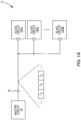
- FIG. 1A is a schematic diagram of an example conventional single-wire bus apparatus 10 in which a master circuit 12 is configured to initiate communications with a number of slave circuits 14(1)-14(M) over a single-wire bus 16, which consists of one conductive wire.
- the master circuit 12 is configured to always initiate a bus telegram communication over the single-wire bus 16
- the conventional single-wire bus apparatus 10 is also known as a "master-slave bus architecture.”
- the slave circuits 14(1)-14(M) may provide a data payload(s) to the master circuit 12 over the single-wire bus 16 in response to receiving a bus telegram(s) from the master circuit 12.
- Each of the slave circuits 14(1)-14(M) is uniquely identified by a respective unique slave identification (USID) that includes multiple bits (e.g., 4 bits).
- the master circuit 12 can initiate a communication with any of the slave circuits 14(1)-14(M) by addressing a bus command sequence to the respective USID. Accordingly, one of the slave circuits 14(1)-14(M) identified by the respective USID can communicate a data payload(s) back to the master circuit 12.
- the master circuit 12 is configured to communicate the bus command sequence to the slave circuits 14(1)-14(M), and the slave circuits 14(1)-14(M) are each configured to communicate the data payload(s) to the master circuit 12, based on a series of bus symbols Ts, which are modulated based on voltage PWM, as illustrated in Figures 1B and 1C.
- Figure 1B is a schematic diagram providing an example illustration of a bus symbol Ts modulated based on voltage PWM to represent a binary value zero ("0").
- the bus symbol Ts is modulated based on a predefined high-voltage interval 18 and a predefined low-voltage interval 20 that are configured according to a predefined configuration ratio.
- the predefined high-voltage interval 18 is shorter than the predefined low-voltage interval 20.
- the bus symbol Ts can include sixteen (16) free-running oscillators (FROs) or 16 digitally controlled oscillators (DCOs) and the predefined configuration ratio between the predefined high-voltage interval 18 and the predefined low-voltage interval 20 is 25% to 75% (or 1 to 3).
- the FROs are derived from a local clock running in the slave circuits 14(1)-14(M) and the DCOs are derived from a clock running at the master circuit 12. Accordingly, the predefined high-voltage interval 18 lasts for four (4) FROs or DCOs and the predefined low-voltage interval 20 lasts for twelve (12) FROs or DCOs.
- a high bus voltage V HIGH is first asserted on the single-wire bus 16 for the predefined high-voltage interval 18 and then a lower bus voltage V LOW is asserted on the single-wire bus 16 for the predefined low-voltage interval 20.
- Figure 1C is a schematic diagram providing an example illustration of a bus symbol Ts modulated to represent a binary value one ("1"). Common elements between Figures 1B and 1C are shown therein with common element numbers and will not be re-described herein.
- the predefined high-voltage interval 18 is longer than the predefined low-voltage interval 20. Based on the same example in Figure 1B , the predefined high-voltage interval 18 lasts for 12 FROs or DCOs and the predefined low-voltage interval 20 lasts for 4 FROs or DCOs. Accordingly, to modulate the bus symbol Ts to represent the binary value "1,” a higher bus voltage V HIGH is first asserted on the single-wire bus 16 for the predefined high-voltage interval 18 and then a lower bus voltage V LOW is asserted on the single-wire bus 16 for the predefined low-voltage interval 20.
- the master circuit 12 In the conventional single-wire bus apparatus 10, communication over the single-wire bus 16 is always initiated by the master circuit 12.
- the master circuit 12 must have the knowledge as to when and what to communicate with the slave circuits 14(1)-14(M) before initiating communications with any of the slave circuits 14(1)-14(M).
- only the slave circuits 14(1)-14(M) have the knowledge as to when and what to communicate over the single-wire bus 16. As such, it is desirable to let any of the slave circuits 14(1)-14(M) initiate communications with the master circuit 12 over the single-wire bus 16.
- FIG 2 is a schematic diagram of an example electronic device 22 that demands slave-initiated communications over a single-wire bus 24.
- the single-wire bus 24 is functionally equivalent to the single-wire bus 16 in the conventional single-wire bus apparatus 10 of Figure 1A .
- the single-wire bus 24 also includes only one conductive wire and can convey a series of bus symbols Ts as modulated in Figures 1B and 1C .
- the electronic device 22 includes a single-wire bus apparatus 26 configured according to embodiments disclosed in the present disclosure to support slave-initiated communications over the single-wire bus 24.
- the single-wire bus apparatus 26 includes a master circuit 28 and multiple slave circuits 30A, 30B, 30C, 30D.
- the slave circuits 30A, 30B, 30C, 30D correspond to a vibrate button, an up button, a down button, and an on/off button in the electronic device 22, respectively.
- each of the slave circuits 30A, 30B, 30C, 30D only needs to communicate with the master circuit 28 in response to a respective data trigger (e.g., pressing of the vibrate button, the up button, the down button, and/or the on/off button), and the master circuit 28 has no knowledge as to when the vibrate button, the up button, the down button, and/or the on/off button is pressed.
- a respective data trigger e.g., pressing of the vibrate button, the up button, the down button, and/or the on/off button
- the slave circuits 30A, 30B, 30C, 30D are each uniquely identified by a respective USID having multiple bits (e.g., 4 bits).
- the slave circuit 30A is identified by USID "1011”
- the slave circuit 30B is identified by USID “1010”
- the slave circuit 30C is identified by USID "1001,”
- the slave circuit 30D is identified by USID "1000.”
- the USID that uniquely identifies each of the slave circuits 30A, 30B, 30C, 30D also defines a priority order for accessing the single-wire bus 24 among the slave circuits 30A, 30B, 30C, 30D. More specifically, the larger the USID, the higher the priority.
- the USID "1011” has a higher priority than the USID “1010,” the USID “1010” has a higher priority than the USID “1001,” and the USID “1001” has a higher priority than the USID “1000.”
- the slave circuit 30A has a higher priority than the slave circuit 30B
- the slave circuit 30B has a higher priority than the slave circuit 30C
- the slave circuit 30C has a higher priority than the slave circuit 30D for accessing the single-wire bus 24.
- the slave circuits 30A, 30B, 30C, 30D are merely provided for the convenience of illustration and reference and shall not be interpreted as limiting by any means. It should be appreciated that the electronic device 22 can be configured to include other numbers and/or types of slave circuits in different implementations.
- the slave circuits can be micro-electromechanical system (MEMS) based devices that are deployed underneath a touchscreen panel and actuated by pressure to initiate communications with the master circuit 28.
- MEMS micro-electromechanical system
- the master circuit 28 maintains the single-wire bus 24 in an idle state if none of the vibrate button, the on/off button, the up button, and the down button is pressed.
- the master circuit 28 may pull the single-wire bus 24 high to maintain a bus voltage V BUS higher than zero volt (V BUS > 0 V). Accordingly, each of the slave circuits 30A, 30B, 30C, 30D can harvest power from the master circuit 28 via the single-wire bus 24 during the idle state.
- one or more of the vibrate button, the up button, the down button, and/or the on/off button may be pressed to necessitate communications with the master circuit 28 over the single-wire bus 24.
- the up button and the on-off button can be concurrently pressed to take a screenshot.
- the up button, the down button, and the on/off button can be pressed in sequence to cause the electronic device 22 to power down.
- the slave circuits 30B, 30C, and 30D must communicate with the master circuit 28 over the single-wire bus 24.
- the slave circuits 30B, 30C, and 30D must contend for an access to the single-wire bus 24 to thereby communicate with the master circuit 28.
- the master circuit 28 must arbitrate and indicate which of the slave circuits 30B, 30C, and 30D will be granted access to the single-wire bus 24 at a given time.
- the master circuit 28 must make sure that the slave circuits 30B, 30C, and 30D are granted access to the single-wire bus 24 in accordance with the sequence in which the up button, the down button, and the on/off button are pressed so as to cause the electronic device 22 to power down.
- the slave circuits 30A, 30B, 30C, 30D may contend for, and the master circuit 28 may grant, the access to the single-wire bus 24 in accordance with predefined bus access sequences.
- Figure 3 is a schematic diagram providing an example illustration of one or more bus access sequences 32, 34 that can be employed by the single-wire bus apparatus 26 in Figure 2 to enable slave-initiated communications over the single-wire bus 24.
- the bus access sequences 32, 34 are shown herein merely for the purpose of illustration. It should be appreciated that the single-wire bus apparatus 26 can operate based on any number of bus access sequences as needed.
- Each of the bus access sequences 32, 34 starts at time T 0 , whereas one or more of the slave circuits 30A, 30B, 30C, 30D assert a wakeup CMS 36 to indicate a request to communicate over the single-wire bus 24.
- each of the slave circuits 30A, 30B, 30C, 30D may assert the wakeup CMS 36 by pulling a current (e.g., for a duration of 3 FROs) from the master circuit 28 over the single-wire bus 24.
- the master circuit 28 In response to detecting the wakeup CMS 36, the master circuit 28 will transmit a start-of-sequence (SOS) sequence 38 (between time T 1 and T 2 ) to all of the slave circuits 30A, 30B, 30C, 30D via the single-wire bus 24.
- SOS start-of-sequence
- Figure 4 is a schematic diagram providing an example illustration of the SOS sequence 38 transmitted by the master circuit 28 in each of the bus access sequences 32, 34 in Figure 3 . Common elements between Figures 3 and 4 are shown and/or referenced therein with common element numbers and will not be re-described herein.
- the master circuit 28 transmits a sync sequence 40 during the SOS sequence 38.
- the SOS sequence 38 is a unique multi-bit pattern that can never be reproduced by any of the slave circuits 30A, 30B, 30C, 30D. Understandably, the multi-bit pattern includes a combination of PWM symbols representing binary "0s" and "1s,” as previously illustrated in Figures 1B and 1C .
- each of the slave circuits 30A, 30B, 30C, 30D Upon successful detection of the sync sequence 40, each of the slave circuits 30A, 30B, 30C, 30D will perform synchronization with the master circuit 28 during a sync interval 42.
- the slave circuits 30A, 30B, 30C, 30D will be able to time-align respective FROs, which are derived from respective local clocks in the slave circuits 30A, 30B, 30C, 30D, with the DCOs generated by the master circuit 28.
- the slave circuits 30A, 30B, 30C, 30D may be configured to opportunistically harvest power from the master circuit 28 via the single-wire bus 24 during reception of the sync sequence 40 and/or the sync interval 42, whenever the bus voltage V BUS is equal to the high bus voltage V HIGH .
- the slave circuits 30A, 30B, 30C, 30D can harvest power from the master circuit 28 during one or more power harvesting intervals 44.
- the power harvesting intervals 44 may not necessarily be started and/or ended at same time for each of the slave circuits 30A, 30B, 30C, 30D.
- the power harvesting intervals 44 may be of a different length for each of the slave circuits 30A, 30B, 30C, 30D.
- each of the bus access sequences 32, 34 also includes an arbitration interval 46 (between time T 2 and T 3 ) that immediately succeeds the SOS sequence 38.
- the master circuit 28 is configured to transmit multiple PWM symbols 48(1)-48(N) that are modulated to uniquely indicate which of the slave circuits 30A, 30B, 30C, 30D is granted access to the single-wire bus 24 during a respective one of the bus access sequences 32, 34.
- Figures 5A , 5B , and 5C are schematic diagrams providing example illustrations as to how the master circuit 28 in the single-wire bus apparatus 26 in Figure 2 grants access to the single-wire bus 24 to one of the slave circuits 30A, 30B, 30C, 30D contending for the single-wire bus 24.
- Common elements between Figures 3 and 5A-5C are shown and/or referenced therein with common element numbers and will not be re-described herein.
- the arbitration interval 46 in each of the bus access sequences 32, 34 is configured to include a priority symbol 50.
- the USID that uniquely identifies each of the slave circuits 30A, 30B, 30C, 30D includes four (4) binary bits.
- the arbitration interval 46 is configured to include multiple USID bit symbols 52A, 52B, 52C, 52D, each representing a respective one of the binary bits in the USID.
- the USID bit symbol 52A which immediately succeeds the priority symbol 50, is configured to represent a most-significant bit (MSB) (e.g., bit #3) in the USID.
- the USID bit symbols 52B, 52C, and 52D will represent bit #2, bit #1, and bit #0 (a.k.a. least-significant bit (LSB)) in the USID, respectively.
- the USID bit symbols 52A, 52B, 52C, 52D will collectively represent the USID “1010” if the USID bit symbols 52A, 52B, 52C, 52D are PWM modulated, as shown in Figures 1B and 1C , to represent binary values "1," "0,” “1,” "0,” respectively.
- the arbitration interval 46 may also include a settle time 53 that precedes the priority symbol 50.
- the settle time 53 may be a one-half (1 ⁇ 2) symbol in duration.
- the slave circuits 30B, 30C, and 30D will contend for the single-wire bus 24 in response to the up button, the down button, and the on/off button being pressed.
- the slave circuits 30B, 30C, and 30D will each indicate the respective USID to the master circuit 28 via the USID bit symbols 52A, 52B, 52C, and 52D.
- each of the slave circuits 30B, 30C, and 30D will assert a bit indication CMS 54 (e.g., for a duration of 2 FROs) in a respective one of the USID bit symbols 52A, 52B, 52C, and 52D if a corresponding bit in the USID has a binary value "1." It should be noted that, during the first attempt to access the single-wire bus 24, none of the slave circuits 30B, 30C, and 30D is allowed to assert the bit indication CMS 54 during the priority symbol 50.
- the slave circuits 32B, 32C, 32D will each assert the bit indication CMS 54 during the USID bit symbol 52A.
- the master circuit 28 will thus modulate the USID bit symbol 52A as illustrated in Figure 1C to represent the binary value "1" in response to detecting the bit indication CMS 54 asserted by the slave circuits 30B, 30C, and 30D.
- the predefined configuration ratio between the predefined high-voltage interval 18 and the predefined low-voltage interval 20 needs to be 75% to 25% to represent the binary value "1.”
- the master circuit 28 is configured to extend the predefined high-voltage interval 18 to 75% of the USID bit symbol 52A to represent the binary value "1" in response to detecting the bit indication CMS 54 asserted by the slave circuits 30B, 30C, and 30D.
- each of the slave circuits 32B, 32C, 32D needs to assert the bit indication CMS 54 as early as possible during the USID bit symbol 52A.
- each of the slave circuits 32B, 32C, 32D asserts the bit indication CMS 54 during a first half of the USID bit symbol 52A.
- the slave circuit 30C is assigned the USID of "1001” and the slave circuit 30D is assigned the USID of "1000.”
- the slave circuits 30C and 30D can conclude that their respective requests for the single-wire bus 24 have failed.
- the slave circuit 30B can continue to contend for the single-wire bus 24.
- the slave circuit 30B will not assert the bit indication CMS 54 since the corresponding bit in the USID "1010" has the binary value "0.”
- the slave circuits 30C and 30D will also not assert the bit indication CMS 54 as a result of losing the request to the slave circuit 30B.
- the master circuit 28 will modulate the USID bit symbol 52D as illustrated in Figure 1B to represent the binary value "0" in response to not detecting the bit indication CMS 54 during the USID bit symbol 52D.
- the master circuit 28 has modulated the USID bit symbols 52A, 52B, 52C, and 52D to collectively represent the USID "1010.”
- the slave circuit 30B can conclude that its request for the single-wire bus 24 has been successful.
- the slave circuits 30C and 30D must continue contending for the single-wire bus 24 in a subsequent bus access sequence.
- Figure 5B illustrates how the slave circuits 30C and 30D can contend for the single-wire bus 24 after failing a previous attempt to access the single-wire bus 24.
- the slave circuits 30C and 30D will each assert the bit indication CMS 54 during the priority symbol 50.
- the master circuit 28 will thus modulate the priority symbol 50 as illustrated in Figure 1C to represent the binary value "1" in response to detecting the bit indication CMS 54 asserted by the slave circuits 30C and 30D.
- the slave circuits 30A and 30B are prohibited from asserting the bit indication CMS 54 in the priority symbol 50. Moreover, the slave circuits 30A and 30B cannot assert the bit indication CMS 54 in any of the USID bit symbols 52A, 52B, 52C, 52D in response to detecting the bit indication CMS 54 in the priority symbol 50.
- the slave circuits 30C and 30D will both assert the bit indication CMS 54 since the corresponding bit in each of the USIDs "1001" and "1000" has the binary value "1.” Accordingly, the master circuit 28 will thus modulate the USID bit symbol 52A to represent the binary value "1" in response to detecting the bit indication CMS 54 asserted by the slave circuits 30C and 30D.
- the slave circuit 30C will assert the bit indication CMS 54 given that the corresponding bit in the USID "1001” once again has the binary value "1.” In the meantime, the slave circuit 30D will not assert the bit indication CMS 54 because the corresponding bit in the USID "1000" has the binary value "0.” Accordingly, the master circuit 28 will modulate the USID bit symbol 52D as illustrated in Figure 1C to represent the binary value "1" in response to detecting the bit indication CMS 54 asserted by the slave circuit 30C.
- the slave circuit 30C can conclude that its request for the single-wire bus 24 has been granted.
- the slave circuit 30D can conclude that its request for the single-wire bus 24 has failed and needs to contend for the single-wire bus 24 once again in a subsequent bus access sequence.
- Figure 5C illustrates how the slave circuit 30D can contend for the single-wire bus 24 after failing two previous attempts to access the single-wire bus 24.
- the slave circuit 32D will assert the bit indication CMS 54 during the priority symbol 50.
- the master circuit 28 will thus modulate the priority symbol 50 as illustrated in Figure 1C to represent the binary value "1" in response to detecting the bit indication CMS 54 asserted by the slave circuit 30D.
- the slave circuits 30A, 30B, and 30C are prohibited from asserting the bit indication CMS 54 in the priority symbol 50. Moreover, the slave circuits 30A, 30B, and 30C cannot assert the bit indication CMS 54 in any of the USID bit symbols 52A, 52B, 52C, 52D in response to detecting the bit indication CMS 54 in the priority symbol 50.
- the slave circuit 30D will assert the bit indication CMS 54 since the corresponding bit in the USID "1000" has the binary value "1.” Accordingly, the master circuit 28 will thus modulate the USID bit symbol 52A to represent the binary value "1" in response to detecting the bit indication CMS 54 asserted by the slave circuit 30D.
- the slave circuit 30D will not assert the bit indication CMS 54 since the corresponding bit in the USID "1000" has the binary value "0.” Accordingly, the master circuit 28 will modulate the USID bit symbols 52B, 52C, and 52D as illustrated in Figure 1B to represent the binary value "0" in response to not detecting the bit indication CMS 54 during the USID bit symbols 52B, 52C, and 52D.
- the slave circuit 30D can conclude that its request for the single-wire bus 24 has been granted. As a result, the slave circuits 30B, 30C, 30D have sequentially gained access to the single-wire bus 24 to thereby cause the electronic device 22 to shut down.
- FIG. 6 is a schematic diagram providing an example illustration of data telegram transmission performed by the slave circuit 30B in the single-wire bus apparatus 26 in Figure 2 over the single-wire bus 24.
- the data telegram 56 includes multiple data symbols 58(1)-58(X).
- the master circuit 28 is configured to modulate each of the data symbols 58(1)-58(X) as the binary value "1" during the data telegram 56 (between time Ts and T 4 ). Accordingly, each of the slave circuits 30A, 30B, 30C, 30D may opportunistically harvest power from the master circuit 28 during multiple power harvesting intervals 60.
- the slave circuit 30B will assert a data CMS 62 if the slave circuit 30B intends to transmit a binary value "1" in any of the data symbols 58(1)-58(X). In contrast, the slave circuit 30B will not assert the data CMS 62 if the slave circuit 30B intends to transmit a binary value "0" in any of the data symbols 58(1)-58(X).
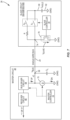
- Figure 7 is a schematic diagram providing an example illustration of the single-wire bus apparatus 26 in the electronic device 22 of Figure 2 configured according to embodiments described in Figures 3 , 4 , 5A-5C , and 6 to support slave-initiated communications over the single-wire bus 24. Common elements between Figures 2 and 7 are shown and/or referenced therein with common element numbers and will not be re-described herein.
- the master circuit 28 includes a bus driver circuit 64 and a receiver circuit 66.
- the bus driver circuit 64 is coupled to the single-wire bus 24.
- the bus driver circuit 64 is configured to pull the single-wire bus 24 high to maintain the bus voltage V BUS during the idle state.
- the bus driver circuit 64 is also configured to detect the wakeup CMS 36 asserted by any of the slave circuits 30A, 30B, 30C, 30D and transmit the SOS sequence 38 in response to detecting the wakeup CMS 36.
- the bus driver circuit 64 is also configured to modulate the priority symbol 50 and the USID bit symbols 52A, 52B, 52C, 52D in the arbitration interval 46 based on the bit indication CMS 54 asserted by any of the slave circuits 30A, 30B, 30C, 30D.
- the bus driver circuit 64 is further configured to modulate each of the data symbols 58(1)-58(X) in the data telegram 56 to represent the binary value "1.”
- the receiver circuit 66 is configured to detect presence or absence of the data CMS 62 transmitted by any of the slave circuits 30A, 30B, 30C, 30D in each of the data symbols 58(1)-58(X) in the data telegram 56. Accordingly, the receiver circuit 66 can output a series of binary "1s" and/or "0s" based on detected presence or absence of the data CMS 62.
- the master circuit 28 also includes a master port 68, a master current sink 70, and a master controller 72.
- the master port 68 is coupled to the single-wire bus 24 and the bus driver circuit 64.
- the master current sink 70 is coupled between the master port 68 and a ground (GND).
- the master controller 72 which can be a microcontroller or a microprocessor for example, is configured to control the bus driver circuit 64 and/or the master current sink 70 to cause the master circuit 28 to modulate the bus symbols Ts (e.g., the sync sequence 40 in Figure 4 , the priority symbol 50 and the USID bit symbols 52A, 52B, 52C, 52D in Figures 5A-5C , and the data symbols 58(1)-58(X) in Figure 6 ) in accordance with the PWM modulation as shown in Figures 1B and 1C .
- the bus symbols Ts e.g., the sync sequence 40 in Figure 4 , the priority symbol 50 and the USID bit symbols 52A, 52B, 52C, 52D in Figures 5A-5C , and the data symbols 58(1)-58(X) in Figure 6
- the bus symbols Ts e.g., the sync sequence 40 in Figure 4 , the priority symbol 50 and the USID bit symbols 52A, 52B, 52C, 52D in Figures 5A-5
- the master circuit 28 may also include an electromagnetic interference (EMI) capacitor C L coupled between the master port 68 and the GND.
- EMI electromagnetic interference
- the EMI capacitor C L corresponds to a total EMI capacitance of the single-wire bus 24, which may vary depending on the number of slave circuits, any added capacitance, and effective capacitance increases due to increased length of the single-wire bus 24.
- the bus driver circuit 64 can be a low dropout (LDO) master current source.
- LDO low dropout
- the master controller 72 To assert the bus voltage V BUS at the low bus voltage V LOW , the master controller 72 is configured to activate the master current sink 70 to induce a sink current I DN to thereby modulate any of the bus symbols Ts (as shown in Figure 1B ) to represent the binary value "0.”
- the master controller 72 is configured to deactivate the master current sink 70. Accordingly, the bus driver circuit 64 will provide a source current I UP to thereby modulate any of the bus symbols Ts (as shown in Figure 1C ) to represent the binary value "1.”
- Each of the slave circuits 30A, 30B, 30C, 30D includes a slave port 74, a slave current sink 76, a holding capacitor C HOLD , and a slave controller 78.
- the slave port 74 is coupled to the single-wire bus 24.
- the slave current sink 76 which can be an N-type transistor for example, is coupled between the slave port 74 and the GND. When the slave current sink 76 is activated, the slave current sink 76 draws a slave current I SLAVE from the master circuit 28.
- the bus driver circuit 64 provides a minimal source current I UP and pulls up the single-wire bus 24 during the idle state.
- any of the slave circuits 30A, 30B, 30C, 30D pulls down the single-wire bus 24 to try to initiate a communication, it is equivalent to receiving data from the slave circuits 30A, 30B, 30C, 30D using the receiver circuit 66.
- the bus driver circuit 64 may provide a voltage indication to the receiver circuit 66 when the source current I UP is pulled down.
- each of the slave circuit 30A, 30B, 30C, 30D can assert the wakeup CMS 36, the bit indication CMS 54, and the data CMS 62 over the single-wire bus 24 by activating the slave current sink 76 (e.g., for different durations) to thereby cause the receiver circuit 66 to receive the bit indication CMS 54, and the data CMS 62.
- the bus driver circuit 64 in the master circuit 28 can detect the wakeup CMS 36, the bit indication CMS 54, and the data CMS 62 and provide corresponding data to the receiver circuit 66.
- the holding capacitor C HOLD has a first end 80 coupled to the slave port 74 via a charge switch S 1 and a second end 82 coupled to the GND.
- the slave controller 78 which can be a microcontroller or a microprocessor for example, is coupled to the slave current sink 76 and the charge switch S 1 .
- the charge switch S 1 will be closed during the power harvesting intervals 44 (as shown in Figure 4 ) and/or the power harvesting intervals 60 (as shown in Figure 6 ) to harvest power from the master circuit 28 to charge up the holding capacitor C HOLD .
- Each of the slave circuits 30A, 30B, 30C, 30D also includes an idle switch S 2 and a resistor R that are coupled in series between the slave port 74 and the first end 80 of the holding capacitor C HOLD .
- the idle switch S 2 is closed when the single-wire bus 24 is in the idle state and opened otherwise.
- each of the slave circuits 30A, 30B, 30C, 30D can harvest power from the master circuit 28 to charge up the holding capacitor C HOLD .
- the idle switch S 2 is opened, the holding capacitor C HOLD will be discharged to supply power to a respective one of the slave circuits 30A, 30B, 30C, 30D.
- the single-wire bus apparatus 26 of Figure 7 can be provided in a user element to support slave-initiated communications over the single-wire bus 24 according to embodiments described above.
- Figure 8 is a schematic diagram of an example user element 100 wherein the single-wire bus apparatus 26 of Figure 7 can be provided to support slave-initiated communications over the single-wire bus 24 in the electronic device 22 of Figure 2 .
- the user element 100 can be any type of user elements, such as mobile terminals, smart watches, tablets, computers, navigation devices, access points, and like wireless communication devices that support wireless communications, such as cellular, wireless local area network (WLAN), Bluetooth, and near field communications.
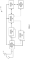
- the user element 100 will generally include a control system 102, a baseband processor 104, transmit circuitry 106, receive circuitry 108, antenna switching circuitry 110, multiple antennas 112, and user interface circuitry 114.
- the control system 102 can be a field-programmable gate array (FPGA), as an example.
- the control system 102 can include at least a microprocessor(s), an embedded memory circuit(s), and a communication bus interface(s).
- the receive circuitry 108 receives radio frequency signals via the antennas 112 and through the antenna switching circuitry 110 from one or more base stations.
- a low noise amplifier and a filter cooperate to amplify and remove broadband interference from the received signal for processing.
- Downconversion and digitization circuitry (not shown) will then downconvert the filtered, received signal to an intermediate or baseband frequency signal, which is then digitized into one or more digital streams using analog-to-digital converter(s) (ADC).
- ADC analog-to-digital converter
- the baseband processor 104 processes the digitized received signal to extract the information or data bits conveyed in the received signal. This processing typically comprises demodulation, decoding, and error correction operations, as will be discussed in greater detail below.
- the baseband processor 104 is generally implemented in one or more digital signal processors (DSPs) and application specific integrated circuits (ASICs).
- DSPs digital signal processors
- ASICs application specific integrated circuits
- the baseband processor 104 receives digitized data, which may represent voice, data, or control information, from the control system 102, which it encodes for transmission.
- the encoded data is output to the transmit circuitry 106, where a digital-to-analog converter(s) (DAC) converts the digitally encoded data into an analog signal and a modulator modulates the analog signal onto a carrier signal that is at a desired transmit frequency or frequencies.
- DAC digital-to-analog converter
- a power amplifier will amplify the modulated carrier signal to a level appropriate for transmission, and deliver the modulated carrier signal to the antennas 112 through the antenna switching circuitry 110.
- the multiple antennas 112 and the replicated transmit and receive circuitries 106, 108 may provide spatial diversity. Modulation and processing details will be understood by those skilled in the art.
- the single-wire bus apparatus 26 of Figure 7 can be further configured to support slave-initiated communications over the single-wire bus 24 according to a process.
- Figure 9 is a flowchart of an example process 200 that can be employed by the single-wire bus apparatus 26 of Figure 7 to support slave-initiated communications over the single-wire bus 24 in the electronic device 22 of Figure 2 .
- any of the slave circuits 30A, 30B, 30C, 30D can assert the wakeup CMS 36 on the single-wire bus 24 to indicate a request to communicate the data telegram 56 over the single-wire bus 24 in response to a respective data trigger (step 202). Accordingly, any of the slave circuits 30A, 30B, 30C, 30D can receive the PWM symbols (Ts) via the single-wire bus 24 in response to asserting the wakeup CMS 36 (step 204). Subsequently, any of the slave circuits 30A, 30B, 30C, 30D can determine whether the request is successful based on the received PWM symbols (Ts) (step 206). Any of the slave circuits 30A, 30B, 30C, 30D is configured to communicate the data telegram 56 over the single-wire bus 24 in response to determining that the request is successful (step 208).
- a single-wire bus apparatus allows a slave circuit(s) to initiate communications over the single-wire bus. More specifically, multiple slave circuits can concurrently contend for access to the single-wire bus via current mode signaling (CMS).
- CMS current mode signaling
- a master circuit provides a number of pulse-width modulation (PWM) symbols over the single-wire bus to indicate which of the multiple slave circuits is granted access to the single-wire bus.
- PWM pulse-width modulation
Landscapes
- Engineering & Computer Science (AREA)
- Theoretical Computer Science (AREA)
- General Engineering & Computer Science (AREA)
- Physics & Mathematics (AREA)
- General Physics & Mathematics (AREA)
- Computer Hardware Design (AREA)
- Computer Networks & Wireless Communication (AREA)
- Signal Processing (AREA)
- Small-Scale Networks (AREA)
- Cable Transmission Systems, Equalization Of Radio And Reduction Of Echo (AREA)
Abstract
Description
- This application claims the benefit of
U.S. provisional patent application serial number 63/301,213, filed on January 20, 2022 application serial number 18/154,127, filed 13 January 2023 - The technology of the disclosure relates generally to slave-initiated communications over a single-wire bus consisting of one wire.
- Mobile communication devices have become increasingly common in current society. The prevalence of these mobile communication devices is driven in part by the many functions that are now enabled on such devices. Increased processing capabilities in such devices means that mobile communication devices have evolved from being pure communication tools into sophisticated mobile multimedia centers that enable enhanced user experiences.
- The redefined user experience requires higher data rates offered by wireless communication technologies, such as Wi-Fi, long-term evolution (LTE), and fifth-generation new-radio (5G-NR). To achieve the higher data rates in mobile communication devices, a mobile communication device may employ a power amplifier(s) to amplify a radio frequency (RF) signal(s) to a higher output power prior to radiating the RF signal via an antenna(s).
- In many mobile communication devices, the power amplifier(s) and the antenna(s) are typically located in an RF front-end (RFFE) circuit communicatively coupled to a transceiver circuit(s) via an RFFE bus as defined in the MIPI® alliance specification for radio frequency front-end control interface, version 2.1.
- Particular aspects are set out in the appended independent claims. Various optional embodiments are set out in the dependent claims.
- From at least some perspectives, the present disclosure can provide for a single-wire bus, either concurrent to or independent of, the RFFE bus in a mobile communication device. Such bus can be used for communications that do not require a two-wire serial bus like the RFFE bus, in such a way that a single-wire serial bus may be enough or even desired for carrying out certain types of communications between circuits.
- Aspects disclosed in the detailed description are related to slave-initiated communications over a single-wire bus. In contrast to a conventional single-wire bus apparatus wherein communications over the single-wire bus are always initiated by a master circuit, a single-wire bus apparatus disclosed herein allows a slave circuit(s) to initiate communications over the single-wire bus. More specifically, multiple slave circuits can concurrently contend for access to the single-wire bus via current mode signaling (CMS). In response to the CMS asserted by the multiple slave circuits, a master circuit provides a number of pulse-width modulation (PWM) symbols over the single-wire bus to indicate which of the multiple slave circuits is granted access to the single-wire bus. By supporting slave-initiated communications over the single-wire bus, it is possible to improve efficiency, cost, and power consumption in an electronic device (e.g., smartphone) wherein the single-wire bus apparatus is deployed.
- In an aspect, a single-wire bus apparatus is provided. The single-wire bus apparatus includes a single-wire bus consisting of one wire. The single-wire bus apparatus also includes multiple slave circuits each coupled to the single-wire bus and uniquely identified by a unique slave identification (USID) comprising multiple bits. One or more slave circuits among the multiple slave circuits are each configured to assert a wakeup CMS on the single-wire bus to indicate a request to communicate a data telegram over the single-wire bus in response to a respective data trigger. The one or more slave circuits among the multiple slave circuits are also each configured to receive multiple PWM symbols via the single-wire bus in response to asserting the wakeup CMS. The one or more slave circuits among the multiple slave circuits are also each configured to determine whether the request is successful based on the multiple received PWM symbols. The one or more slave circuits among the multiple slave circuits are also each configured to communicate the data telegram over the single-wire bus in response to determining that the request is successful.
- In another aspect, a method for supporting slave-initiated communications over a single-wire bus is provided. The method includes asserting a wakeup CMS on the single-wire bus to indicate a request to communicate a data telegram over the single-wire bus in response to a respective data trigger. The method also includes receiving a plurality of PWM symbols via the single-wire bus in response to asserting the wakeup CMS. The method also includes determining whether the request is successful based on the plurality of received PWM symbols. The method also includes communicating the data telegram over the single-wire bus in response to determining that the request is successful.
- Those skilled in the art will appreciate the scope of the disclosure and realize additional aspects thereof after reading the following detailed description in association with the accompanying drawings.
- The accompanying drawings incorporated in and forming a part of this specification illustrate several aspects of the disclosure and, together with the description, serve to explain the principles of the disclosure.
-
Figure 1A is a schematic diagram of an example conventional single-wire bus apparatus in which a master circuit is configured to initiate communications with a number of slave circuits over a single-wire bus; -
Figure 1B is a schematic diagram providing an example illustration of a bus symbol modulated based on voltage pulse-width modulation (PWM) to represent a binary value zero ("0"); -
Figure 1C is a schematic diagram providing an example illustration of a bus symbol modulated based on voltage PWM to represent a binary value one ("1"); -
Figure 2 is a schematic diagram of an example electronic device that demands slave-initiated communications over a single-wire bus; -
Figure 3 is a schematic diagram providing an example illustration of one or more bus access sequences that can be employed by the electronic device ofFigure 2 to enable slave-initiated communications over the single-wire bus; -
Figure 4 is a schematic diagram providing an example illustration of a start-of-sequence (SOS) sequence transmitted in each of the bus access sequences inFigure 3 ; -
Figures 5A-5C are schematic diagrams providing example illustrations as to how a master circuit in the electronic device ofFigure 2 grants access to the single-wire bus to one of multiple slave circuits contending for the single-wire bus; -
Figure 6 is a schematic diagram providing an example illustration of data telegram transmission performed by a slave circuit in the electronic device ofFigure 2 over the single-wire bus; -
Figure 7 is a schematic diagram of an example single-wire bus apparatus configured according to embodiments described inFigures 3 ,4 ,5A-5C , and6 to support slave-initiated communications over the single-wire bus in the electronic device ofFigure 2 ; -
Figure 8 is a schematic diagram of an example user element wherein the single-wire bus apparatus ofFigure 7 can be provided to support slave-initiated communications over the single-wire bus in the electronic device ofFigure 2 ; and -
Figure 9 is a flowchart of an example process that can be employed by the single-wire bus apparatus ofFigure 7 to support slave-initiated communications over the single-wire bus in the electronic device ofFigure 2 . - The embodiments set forth below represent the necessary information to enable those skilled in the art to practice the embodiments and illustrate the best mode of practicing the embodiments. Upon reading the following description in light of the accompanying drawing figures, those skilled in the art will understand the concepts of the disclosure and will recognize applications of these concepts not particularly addressed herein. It should be understood that these concepts and applications fall within the scope of the disclosure and the accompanying claims.
- It will be understood that, although the terms first, second, etc. may be used herein to describe various elements, these elements should not be limited by these terms. These terms are only used to distinguish one element from another. For example, a first element could be termed a second element, and, similarly, a second element could be termed a first element, without departing from the scope of the present disclosure. As used herein, the term "and/or" includes any and all combinations of one or more of the associated listed items.
- It will be understood that when an element such as a layer, region, or substrate is referred to as being "on" or extending "onto" another element, it can be directly on or extend directly onto the other element or intervening elements may also be present. In contrast, when an element is referred to as being "directly on" or extending "directly onto" another element, there are no intervening elements present. Likewise, it will be understood that when an element such as a layer, region, or substrate is referred to as being "over" or extending "over" another element, it can be directly over or extend directly over the other element or intervening elements may also be present. In contrast, when an element is referred to as being "directly over" or extending "directly over" another element, there are no intervening elements present. It will also be understood that when an element is referred to as being "connected" or "coupled" to another element, it can be directly connected or coupled to the other element or intervening elements may be present. In contrast, when an element is referred to as being "directly connected" or "directly coupled" to another element, there are no intervening elements present.
- Relative terms such as "below" or "above" or "upper" or "lower" or "horizontal" or "vertical" may be used herein to describe a relationship of one element, layer, or region to another element, layer, or region as illustrated in the Figures. It will be understood that these terms and those discussed above are intended to encompass different orientations of the device in addition to the orientation depicted in the Figures.
- The terminology used herein is for the purpose of describing particular embodiments only and is not intended to be limiting of the disclosure. As used herein, the singular forms "a," "an," and "the" are intended to include the plural forms as well, unless the context clearly indicates otherwise. It will be further understood that the terms "comprises," "comprising," "includes," and/or "including" when used herein specify the presence of stated features, integers, steps, operations, elements, and/or components, but do not preclude the presence or addition of one or more other features, integers, steps, operations, elements, components, and/or groups thereof.
- Unless otherwise defined, all terms (including technical and scientific terms) used herein have the same meaning as commonly understood by one of ordinary skill in the art to which this disclosure belongs. It will be further understood that terms used herein should be interpreted as having a meaning that is consistent with their meaning in the context of this specification and the relevant art and will not be interpreted in an idealized or overly formal sense unless expressly so defined herein.
- Aspects disclosed in the detailed description are related to slave-initiated communications over a single-wire bus. In contrast to a conventional single-wire bus apparatus wherein communications over the single-wire bus are always initiated by a master circuit, a single-wire bus apparatus disclosed herein allows a slave circuit(s) to initiate communications over the single-wire bus. More specifically, multiple slave circuits can concurrently contend for access to the single-wire bus via current mode signaling (CMS). In response to the CMS asserted by the multiple slave circuits, a master circuit provides a number of pulse-width modulation (PWM) symbols over the single-wire bus to indicate which of the multiple slave circuits is granted access to the single-wire bus. By supporting slave-initiated communications over the single-wire bus, it is possible to improve efficiency, cost, and power consumption in an electronic device (e.g., smartphone) wherein the single-wire bus apparatus is deployed.
- Before discussing a single-wire bus apparatus of the present disclosure, starting at
Figure 2 , a brief overview of a conventional single-wire bus apparatus is first provided with reference toFigures 1A-1C to help understand basic operations of the conventional single-wire bus and formats of a PWM symbol. - In this regard,
Figure 1A is a schematic diagram of an example conventional single-wire bus apparatus 10 in which amaster circuit 12 is configured to initiate communications with a number of slave circuits 14(1)-14(M) over a single-wire bus 16, which consists of one conductive wire. Given that themaster circuit 12 is configured to always initiate a bus telegram communication over the single-wire bus 16, the conventional single-wire bus apparatus 10 is also known as a "master-slave bus architecture." The slave circuits 14(1)-14(M) may provide a data payload(s) to themaster circuit 12 over the single-wire bus 16 in response to receiving a bus telegram(s) from themaster circuit 12. - Each of the slave circuits 14(1)-14(M) is uniquely identified by a respective unique slave identification (USID) that includes multiple bits (e.g., 4 bits). In this regard, the
master circuit 12 can initiate a communication with any of the slave circuits 14(1)-14(M) by addressing a bus command sequence to the respective USID. Accordingly, one of the slave circuits 14(1)-14(M) identified by the respective USID can communicate a data payload(s) back to themaster circuit 12. - In the conventional single-
wire bus apparatus 10, themaster circuit 12 is configured to communicate the bus command sequence to the slave circuits 14(1)-14(M), and the slave circuits 14(1)-14(M) are each configured to communicate the data payload(s) to themaster circuit 12, based on a series of bus symbols Ts, which are modulated based on voltage PWM, as illustrated inFigures 1B and 1C. Figure 1B is a schematic diagram providing an example illustration of a bus symbol Ts modulated based on voltage PWM to represent a binary value zero ("0"). - In an embodiment, the bus symbol Ts is modulated based on a predefined high-
voltage interval 18 and a predefined low-voltage interval 20 that are configured according to a predefined configuration ratio. To represent the binary value "0," the predefined high-voltage interval 18 is shorter than the predefined low-voltage interval 20. For example, the bus symbol Ts can include sixteen (16) free-running oscillators (FROs) or 16 digitally controlled oscillators (DCOs) and the predefined configuration ratio between the predefined high-voltage interval 18 and the predefined low-voltage interval 20 is 25% to 75% (or 1 to 3). In a non-limiting example, the FROs are derived from a local clock running in the slave circuits 14(1)-14(M) and the DCOs are derived from a clock running at themaster circuit 12. Accordingly, the predefined high-voltage interval 18 lasts for four (4) FROs or DCOs and the predefined low-voltage interval 20 lasts for twelve (12) FROs or DCOs. - In this regard, to modulate the bus symbol Ts to represent the binary value "0," a high bus voltage VHIGH is first asserted on the single-
wire bus 16 for the predefined high-voltage interval 18 and then a lower bus voltage VLOW is asserted on the single-wire bus 16 for the predefined low-voltage interval 20. -
Figure 1C is a schematic diagram providing an example illustration of a bus symbol Ts modulated to represent a binary value one ("1"). Common elements betweenFigures 1B and 1C are shown therein with common element numbers and will not be re-described herein. - To represent the voltage PWM value "1," the predefined high-
voltage interval 18 is longer than the predefined low-voltage interval 20. Based on the same example inFigure 1B , the predefined high-voltage interval 18 lasts for 12 FROs or DCOs and the predefined low-voltage interval 20 lasts for 4 FROs or DCOs. Accordingly, to modulate the bus symbol Ts to represent the binary value "1," a higher bus voltage VHIGH is first asserted on the single-wire bus 16 for the predefined high-voltage interval 18 and then a lower bus voltage VLOW is asserted on the single-wire bus 16 for the predefined low-voltage interval 20. - In the conventional single-
wire bus apparatus 10, communication over the single-wire bus 16 is always initiated by themaster circuit 12. In this regard, themaster circuit 12 must have the knowledge as to when and what to communicate with the slave circuits 14(1)-14(M) before initiating communications with any of the slave circuits 14(1)-14(M). However, in some implementations, only the slave circuits 14(1)-14(M) have the knowledge as to when and what to communicate over the single-wire bus 16. As such, it is desirable to let any of the slave circuits 14(1)-14(M) initiate communications with themaster circuit 12 over the single-wire bus 16. -
Figure 2 is a schematic diagram of an exampleelectronic device 22 that demands slave-initiated communications over a single-wire bus 24. Herein, the single-wire bus 24 is functionally equivalent to the single-wire bus 16 in the conventional single-wire bus apparatus 10 ofFigure 1A . In this regard, the single-wire bus 24 also includes only one conductive wire and can convey a series of bus symbols Ts as modulated inFigures 1B and 1C . - The
electronic device 22 includes a single-wire bus apparatus 26 configured according to embodiments disclosed in the present disclosure to support slave-initiated communications over the single-wire bus 24. In an embodiment, the single-wire bus apparatus 26 includes amaster circuit 28 andmultiple slave circuits slave circuits electronic device 22, respectively. In this regard, each of theslave circuits master circuit 28 in response to a respective data trigger (e.g., pressing of the vibrate button, the up button, the down button, and/or the on/off button), and themaster circuit 28 has no knowledge as to when the vibrate button, the up button, the down button, and/or the on/off button is pressed. - Similar to the slave circuits 14(1)-14(M) in
Figure 1A , theslave circuits slave circuit 30A is identified by USID "1011," theslave circuit 30B is identified by USID "1010," theslave circuit 30C is identified by USID "1001," and theslave circuit 30D is identified by USID "1000." - In embodiments disclosed hereinafter, the USID that uniquely identifies each of the
slave circuits wire bus 24 among theslave circuits slave circuits slave circuit 30A has a higher priority than theslave circuit 30B, theslave circuit 30B has a higher priority than theslave circuit 30C, and theslave circuit 30C has a higher priority than theslave circuit 30D for accessing the single-wire bus 24. - Notably, the
slave circuits electronic device 22 can be configured to include other numbers and/or types of slave circuits in different implementations. For example, the slave circuits can be micro-electromechanical system (MEMS) based devices that are deployed underneath a touchscreen panel and actuated by pressure to initiate communications with themaster circuit 28. - The
master circuit 28 maintains the single-wire bus 24 in an idle state if none of the vibrate button, the on/off button, the up button, and the down button is pressed. In an embodiment, themaster circuit 28 may pull the single-wire bus 24 high to maintain a bus voltage VBUS higher than zero volt (VBUS > 0 V). Accordingly, each of theslave circuits master circuit 28 via the single-wire bus 24 during the idle state. - At any given time, one or more of the vibrate button, the up button, the down button, and/or the on/off button may be pressed to necessitate communications with the
master circuit 28 over the single-wire bus 24. In one example, the up button and the on-off button can be concurrently pressed to take a screenshot. In another example, the up button, the down button, and the on/off button can be pressed in sequence to cause theelectronic device 22 to power down. - In the example of powering down the
electronic device 22, theslave circuits master circuit 28 over the single-wire bus 24. In this regard, theslave circuits wire bus 24 to thereby communicate with themaster circuit 28. In response, themaster circuit 28 must arbitrate and indicate which of theslave circuits wire bus 24 at a given time. Moreover, themaster circuit 28 must make sure that theslave circuits wire bus 24 in accordance with the sequence in which the up button, the down button, and the on/off button are pressed so as to cause theelectronic device 22 to power down. - According to an embodiment of the present disclosure, the
slave circuits master circuit 28 may grant, the access to the single-wire bus 24 in accordance with predefined bus access sequences. In this regard,Figure 3 is a schematic diagram providing an example illustration of one or more bus access sequences 32, 34 that can be employed by the single-wire bus apparatus 26 inFigure 2 to enable slave-initiated communications over the single-wire bus 24. Notably, the bus access sequences 32, 34 are shown herein merely for the purpose of illustration. It should be appreciated that the single-wire bus apparatus 26 can operate based on any number of bus access sequences as needed. - Each of the bus access sequences 32, 34 starts at time T0, whereas one or more of the
slave circuits wakeup CMS 36 to indicate a request to communicate over the single-wire bus 24. In a non-limiting example, each of theslave circuits wakeup CMS 36 by pulling a current (e.g., for a duration of 3 FROs) from themaster circuit 28 over the single-wire bus 24. - In response to detecting the
wakeup CMS 36, themaster circuit 28 will transmit a start-of-sequence (SOS) sequence 38 (between time T1 and T2) to all of theslave circuits wire bus 24.Figure 4 is a schematic diagram providing an example illustration of theSOS sequence 38 transmitted by themaster circuit 28 in each of the bus access sequences 32, 34 inFigure 3 . Common elements betweenFigures 3 and4 are shown and/or referenced therein with common element numbers and will not be re-described herein. - In an embodiment, the
master circuit 28 transmits async sequence 40 during theSOS sequence 38. TheSOS sequence 38 is a unique multi-bit pattern that can never be reproduced by any of theslave circuits Figures 1B and 1C . Upon successful detection of thesync sequence 40, each of theslave circuits master circuit 28 during async interval 42. As a result, at time T2, theslave circuits slave circuits master circuit 28. - Additionally, the
slave circuits master circuit 28 via the single-wire bus 24 during reception of thesync sequence 40 and/or thesync interval 42, whenever the bus voltage VBUS is equal to the high bus voltage VHIGH. For example, theslave circuits master circuit 28 during one or morepower harvesting intervals 44. Notably, thepower harvesting intervals 44 may not necessarily be started and/or ended at same time for each of theslave circuits power harvesting intervals 44 may be of a different length for each of theslave circuits - With reference back to
Figure 3 , each of the bus access sequences 32, 34 also includes an arbitration interval 46 (between time T2 and T3) that immediately succeeds theSOS sequence 38. During thearbitration interval 46 in each of the bus access sequences 32, 34, themaster circuit 28 is configured to transmit multiple PWM symbols 48(1)-48(N) that are modulated to uniquely indicate which of theslave circuits wire bus 24 during a respective one of the bus access sequences 32, 34. -
Figures 5A ,5B , and5C are schematic diagrams providing example illustrations as to how themaster circuit 28 in the single-wire bus apparatus 26 inFigure 2 grants access to the single-wire bus 24 to one of theslave circuits wire bus 24. Common elements betweenFigures 3 and5A-5C are shown and/or referenced therein with common element numbers and will not be re-described herein. - With reference to
Figure 5A , in an embodiment, thearbitration interval 46 in each of the bus access sequences 32, 34 is configured to include apriority symbol 50. In an embodiment, the USID that uniquely identifies each of theslave circuits arbitration interval 46 is configured to include multipleUSID bit symbols USID bit symbol 52A, which immediately succeeds thepriority symbol 50, is configured to represent a most-significant bit (MSB) (e.g., bit #3) in the USID. Accordingly, theUSID bit symbols bit # 2,bit # 1, and bit #0 (a.k.a. least-significant bit (LSB)) in the USID, respectively. For example, theUSID bit symbols USID bit symbols Figures 1B and 1C , to represent binary values "1," "0," "1," "0," respectively. - The
arbitration interval 46 may also include asettle time 53 that precedes thepriority symbol 50. Thesettle time 53 may be a one-half (½) symbol in duration. - Continuing with the example of powering down the
electronic device 22, theslave circuits wire bus 24 in response to the up button, the down button, and the on/off button being pressed. According to an embodiment of the present disclosure, in a first attempt to access the single-wire bus 24, theslave circuits master circuit 28 via theUSID bit symbols slave circuits USID bit symbols wire bus 24, none of theslave circuits bit indication CMS 54 during thepriority symbol 50. - For example, since the USID of the
slave circuit 30B is "1010," the USID of theslave circuit 30C is "1001," and the USID of theslave circuit 30D is "1000," the slave circuits 32B, 32C, 32D will each assert thebit indication CMS 54 during theUSID bit symbol 52A. Themaster circuit 28 will thus modulate theUSID bit symbol 52A as illustrated inFigure 1C to represent the binary value "1" in response to detecting thebit indication CMS 54 asserted by theslave circuits Figures 1B and 1C , the predefined configuration ratio between the predefined high-voltage interval 18 and the predefined low-voltage interval 20 needs to be 75% to 25% to represent the binary value "1." In this regard, in one aspect, themaster circuit 28 is configured to extend the predefined high-voltage interval 18 to 75% of theUSID bit symbol 52A to represent the binary value "1" in response to detecting thebit indication CMS 54 asserted by theslave circuits bit indication CMS 54 as early as possible during theUSID bit symbol 52A. In a non-limiting example, each of the slave circuits 32B, 32C, 32D asserts thebit indication CMS 54 during a first half of theUSID bit symbol 52A. - In the
USID bit symbol 52B, none of theslave circuits bit indication CMS 54 since the corresponding bit in each of the USIDs "1010," "1001," and "1000" has a binary value "0." Accordingly, themaster circuit 28 will modulate theUSID bit symbol 52B as illustrated inFigure 1B to represent the binary value "0" in response to not detecting thebit indication CMS 54 during theUSID bit symbol 52B. - In the
USID bit symbol 52C, only theslave circuit 30B will assert thebit indication CMS 54 given that the corresponding bit in the USID "1010" once again has the binary value "1." In the meantime, theslave circuits bit indication CMS 54 because the corresponding bit in the USIDs "1001" and "1000" both have the binary value "0." Accordingly, themaster circuit 28 will modulate theUSID bit symbol 52C as illustrated inFigure 1C to represent the binary value "1" in response to detecting thebit indication CMS 54 asserted by theslave circuit 30B. - As mentioned earlier, the
slave circuit 30C is assigned the USID of "1001" and theslave circuit 30D is assigned the USID of "1000." As such, by modulating theUSID bit symbol 52C to represent the binary value "1," theslave circuits wire bus 24 have failed. In the meantime, theslave circuit 30B can continue to contend for the single-wire bus 24. - In the
USID bit symbol 52D, theslave circuit 30B will not assert thebit indication CMS 54 since the corresponding bit in the USID "1010" has the binary value "0." Theslave circuits bit indication CMS 54 as a result of losing the request to theslave circuit 30B. Accordingly, themaster circuit 28 will modulate theUSID bit symbol 52D as illustrated inFigure 1B to represent the binary value "0" in response to not detecting thebit indication CMS 54 during theUSID bit symbol 52D. At this point, themaster circuit 28 has modulated theUSID bit symbols slave circuit 30B can conclude that its request for the single-wire bus 24 has been successful. Theslave circuits wire bus 24 in a subsequent bus access sequence. -
Figure 5B illustrates how theslave circuits wire bus 24 after failing a previous attempt to access the single-wire bus 24. As a second attempt to access the single-wire bus 24, theslave circuits bit indication CMS 54 during thepriority symbol 50. Themaster circuit 28 will thus modulate thepriority symbol 50 as illustrated inFigure 1C to represent the binary value "1" in response to detecting thebit indication CMS 54 asserted by theslave circuits - Notably, the
slave circuits bit indication CMS 54 in thepriority symbol 50. Moreover, theslave circuits bit indication CMS 54 in any of theUSID bit symbols bit indication CMS 54 in thepriority symbol 50. - In the
USID bit symbol 52A, theslave circuits bit indication CMS 54 since the corresponding bit in each of the USIDs "1001" and "1000" has the binary value "1." Accordingly, themaster circuit 28 will thus modulate theUSID bit symbol 52A to represent the binary value "1" in response to detecting thebit indication CMS 54 asserted by theslave circuits USID bit symbols slave circuits bit indication CMS 54 since the corresponding bits in each of the USIDs "1001" and "1000" has the binary value "0." Accordingly, themaster circuit 28 will modulate theUSID bit symbols Figure 1B to represent the binary value "0" in response to not detecting thebit indication CMS 54 during theUSID bit symbols - In the
USID bit symbol 52D, theslave circuit 30C will assert thebit indication CMS 54 given that the corresponding bit in the USID "1001" once again has the binary value "1." In the meantime, theslave circuit 30D will not assert thebit indication CMS 54 because the corresponding bit in the USID "1000" has the binary value "0." Accordingly, themaster circuit 28 will modulate theUSID bit symbol 52D as illustrated inFigure 1C to represent the binary value "1" in response to detecting thebit indication CMS 54 asserted by theslave circuit 30C. Thus, by asserting thebit indication CMS 54 during thepriority symbol 50 and detecting theUSID bit symbols slave circuit 30C can conclude that its request for the single-wire bus 24 has been granted. In contrast, theslave circuit 30D can conclude that its request for the single-wire bus 24 has failed and needs to contend for the single-wire bus 24 once again in a subsequent bus access sequence. -
Figure 5C illustrates how theslave circuit 30D can contend for the single-wire bus 24 after failing two previous attempts to access the single-wire bus 24. As a third attempt to access the single-wire bus 24, the slave circuit 32D will assert thebit indication CMS 54 during thepriority symbol 50. Themaster circuit 28 will thus modulate thepriority symbol 50 as illustrated inFigure 1C to represent the binary value "1" in response to detecting thebit indication CMS 54 asserted by theslave circuit 30D. - Notably, the
slave circuits bit indication CMS 54 in thepriority symbol 50. Moreover, theslave circuits bit indication CMS 54 in any of theUSID bit symbols bit indication CMS 54 in thepriority symbol 50. - In the
USID bit symbol 52A, theslave circuit 30D will assert thebit indication CMS 54 since the corresponding bit in the USID "1000" has the binary value "1." Accordingly, themaster circuit 28 will thus modulate theUSID bit symbol 52A to represent the binary value "1" in response to detecting thebit indication CMS 54 asserted by theslave circuit 30D. In theUSID bit symbols slave circuit 30D will not assert thebit indication CMS 54 since the corresponding bit in the USID "1000" has the binary value "0." Accordingly, themaster circuit 28 will modulate theUSID bit symbols Figure 1B to represent the binary value "0" in response to not detecting thebit indication CMS 54 during theUSID bit symbols bit indication CMS 54 during thepriority symbol 50 and detecting theUSID bit symbols slave circuit 30D can conclude that its request for the single-wire bus 24 has been granted. As a result, theslave circuits wire bus 24 to thereby cause theelectronic device 22 to shut down. - With reference back to
Figure 3 , upon successful request for the single-wire bus 24 in a respective bus access sequence (e.g., the bus access sequence 32, 34, and so on), theslave circuits data telegram 56 over the single-wire bus 24 (between time Ts and T4). In this regard,Figure 6 is a schematic diagram providing an example illustration of data telegram transmission performed by theslave circuit 30B in the single-wire bus apparatus 26 inFigure 2 over the single-wire bus 24. - The
data telegram 56 includes multiple data symbols 58(1)-58(X). In an embodiment, themaster circuit 28 is configured to modulate each of the data symbols 58(1)-58(X) as the binary value "1" during the data telegram 56 (between time Ts and T4). Accordingly, each of theslave circuits master circuit 28 during multiplepower harvesting intervals 60. - The
slave circuit 30B will assert adata CMS 62 if theslave circuit 30B intends to transmit a binary value "1" in any of the data symbols 58(1)-58(X). In contrast, theslave circuit 30B will not assert thedata CMS 62 if theslave circuit 30B intends to transmit a binary value "0" in any of the data symbols 58(1)-58(X). -
Figure 7 is a schematic diagram providing an example illustration of the single-wire bus apparatus 26 in theelectronic device 22 ofFigure 2 configured according to embodiments described inFigures 3 ,4 ,5A-5C , and6 to support slave-initiated communications over the single-wire bus 24. Common elements betweenFigures 2 and7 are shown and/or referenced therein with common element numbers and will not be re-described herein. - The
master circuit 28 includes abus driver circuit 64 and areceiver circuit 66. Thebus driver circuit 64 is coupled to the single-wire bus 24. Thebus driver circuit 64 is configured to pull the single-wire bus 24 high to maintain the bus voltage VBUS during the idle state. Thebus driver circuit 64 is also configured to detect thewakeup CMS 36 asserted by any of theslave circuits SOS sequence 38 in response to detecting thewakeup CMS 36. Thebus driver circuit 64 is also configured to modulate thepriority symbol 50 and theUSID bit symbols arbitration interval 46 based on thebit indication CMS 54 asserted by any of theslave circuits bus driver circuit 64 is further configured to modulate each of the data symbols 58(1)-58(X) in thedata telegram 56 to represent the binary value "1." - The
receiver circuit 66 is configured to detect presence or absence of thedata CMS 62 transmitted by any of theslave circuits data telegram 56. Accordingly, thereceiver circuit 66 can output a series of binary "1s" and/or "0s" based on detected presence or absence of thedata CMS 62. - The
master circuit 28 also includes amaster port 68, a mastercurrent sink 70, and amaster controller 72. Themaster port 68 is coupled to the single-wire bus 24 and thebus driver circuit 64. The mastercurrent sink 70 is coupled between themaster port 68 and a ground (GND). Themaster controller 72, which can be a microcontroller or a microprocessor for example, is configured to control thebus driver circuit 64 and/or the mastercurrent sink 70 to cause themaster circuit 28 to modulate the bus symbols Ts (e.g., thesync sequence 40 inFigure 4 , thepriority symbol 50 and theUSID bit symbols Figures 5A-5C , and the data symbols 58(1)-58(X) inFigure 6 ) in accordance with the PWM modulation as shown inFigures 1B and 1C . - The
master circuit 28 may also include an electromagnetic interference (EMI) capacitor CL coupled between themaster port 68 and the GND. Notably, the EMI capacitor CL corresponds to a total EMI capacitance of the single-wire bus 24, which may vary depending on the number of slave circuits, any added capacitance, and effective capacitance increases due to increased length of the single-wire bus 24. - In one embodiment, the
bus driver circuit 64 can be a low dropout (LDO) master current source. To assert the bus voltage VBUS at the low bus voltage VLOW, themaster controller 72 is configured to activate the mastercurrent sink 70 to induce a sink current IDN to thereby modulate any of the bus symbols Ts (as shown inFigure 1B ) to represent the binary value "0." In contrast, to raise the bus voltage VBUS to the high bus voltage VHIGH, themaster controller 72 is configured to deactivate the mastercurrent sink 70. Accordingly, thebus driver circuit 64 will provide a source current IUP to thereby modulate any of the bus symbols Ts (as shown inFigure 1C ) to represent the binary value "1." - Each of the
slave circuits slave port 74, a slavecurrent sink 76, a holding capacitor CHOLD, and aslave controller 78. Theslave port 74 is coupled to the single-wire bus 24. The slavecurrent sink 76, which can be an N-type transistor for example, is coupled between theslave port 74 and the GND. When the slavecurrent sink 76 is activated, the slavecurrent sink 76 draws a slave current ISLAVE from themaster circuit 28. Thebus driver circuit 64 provides a minimal source current IUP and pulls up the single-wire bus 24 during the idle state. When any of theslave circuits wire bus 24 to try to initiate a communication, it is equivalent to receiving data from theslave circuits receiver circuit 66. Thebus driver circuit 64 may provide a voltage indication to thereceiver circuit 66 when the source current IUP is pulled down. - In this regard, each of the
slave circuit wakeup CMS 36, thebit indication CMS 54, and thedata CMS 62 over the single-wire bus 24 by activating the slave current sink 76 (e.g., for different durations) to thereby cause thereceiver circuit 66 to receive thebit indication CMS 54, and thedata CMS 62. Accordingly, thebus driver circuit 64 in themaster circuit 28 can detect thewakeup CMS 36, thebit indication CMS 54, and thedata CMS 62 and provide corresponding data to thereceiver circuit 66. - The holding capacitor CHOLD has a
first end 80 coupled to theslave port 74 via a charge switch S1 and asecond end 82 coupled to the GND. Theslave controller 78, which can be a microcontroller or a microprocessor for example, is coupled to the slavecurrent sink 76 and the charge switch S1. The charge switch S1 will be closed during the power harvesting intervals 44 (as shown inFigure 4 ) and/or the power harvesting intervals 60 (as shown inFigure 6 ) to harvest power from themaster circuit 28 to charge up the holding capacitor CHOLD. - Each of the
slave circuits slave port 74 and thefirst end 80 of the holding capacitor CHOLD. The idle switch S2 is closed when the single-wire bus 24 is in the idle state and opened otherwise. When the idle switch S2 is closed, each of theslave circuits master circuit 28 to charge up the holding capacitor CHOLD. In contrast, when the idle switch S2 is opened, the holding capacitor CHOLD will be discharged to supply power to a respective one of theslave circuits - The single-
wire bus apparatus 26 ofFigure 7 can be provided in a user element to support slave-initiated communications over the single-wire bus 24 according to embodiments described above. In this regard,Figure 8 is a schematic diagram of anexample user element 100 wherein the single-wire bus apparatus 26 ofFigure 7 can be provided to support slave-initiated communications over the single-wire bus 24 in theelectronic device 22 ofFigure 2 . - Herein, the
user element 100 can be any type of user elements, such as mobile terminals, smart watches, tablets, computers, navigation devices, access points, and like wireless communication devices that support wireless communications, such as cellular, wireless local area network (WLAN), Bluetooth, and near field communications. Theuser element 100 will generally include acontrol system 102, abaseband processor 104, transmitcircuitry 106, receivecircuitry 108,antenna switching circuitry 110,multiple antennas 112, anduser interface circuitry 114. In a non-limiting example, thecontrol system 102 can be a field-programmable gate array (FPGA), as an example. In this regard, thecontrol system 102 can include at least a microprocessor(s), an embedded memory circuit(s), and a communication bus interface(s). The receivecircuitry 108 receives radio frequency signals via theantennas 112 and through theantenna switching circuitry 110 from one or more base stations. A low noise amplifier and a filter cooperate to amplify and remove broadband interference from the received signal for processing. Downconversion and digitization circuitry (not shown) will then downconvert the filtered, received signal to an intermediate or baseband frequency signal, which is then digitized into one or more digital streams using analog-to-digital converter(s) (ADC). - The
baseband processor 104 processes the digitized received signal to extract the information or data bits conveyed in the received signal. This processing typically comprises demodulation, decoding, and error correction operations, as will be discussed in greater detail below. Thebaseband processor 104 is generally implemented in one or more digital signal processors (DSPs) and application specific integrated circuits (ASICs). - For transmission, the
baseband processor 104 receives digitized data, which may represent voice, data, or control information, from thecontrol system 102, which it encodes for transmission. The encoded data is output to the transmitcircuitry 106, where a digital-to-analog converter(s) (DAC) converts the digitally encoded data into an analog signal and a modulator modulates the analog signal onto a carrier signal that is at a desired transmit frequency or frequencies. A power amplifier will amplify the modulated carrier signal to a level appropriate for transmission, and deliver the modulated carrier signal to theantennas 112 through theantenna switching circuitry 110. Themultiple antennas 112 and the replicated transmit and receivecircuitries - The single-
wire bus apparatus 26 ofFigure 7 can be further configured to support slave-initiated communications over the single-wire bus 24 according to a process. In this regard,Figure 9 is a flowchart of anexample process 200 that can be employed by the single-wire bus apparatus 26 ofFigure 7 to support slave-initiated communications over the single-wire bus 24 in theelectronic device 22 ofFigure 2 . - Herein, any of the
slave circuits wakeup CMS 36 on the single-wire bus 24 to indicate a request to communicate thedata telegram 56 over the single-wire bus 24 in response to a respective data trigger (step 202). Accordingly, any of theslave circuits wire bus 24 in response to asserting the wakeup CMS 36 (step 204). Subsequently, any of theslave circuits slave circuits data telegram 56 over the single-wire bus 24 in response to determining that the request is successful (step 208). - Those skilled in the art will recognize improvements and modifications to the embodiments of the present disclosure. All such improvements and modifications are considered within the scope of the concepts disclosed herein and the claims that follow.
- Therefore, from one perspective, there have been described approaches for slave-initiated communications over a single-wire bus. In contrast to a conventional single-wire bus apparatus wherein communications over the single-wire bus are always initiated by a master circuit, a single-wire bus apparatus disclosed herein allows a slave circuit(s) to initiate communications over the single-wire bus. More specifically, multiple slave circuits can concurrently contend for access to the single-wire bus via current mode signaling (CMS). In response to the CMS asserted by the multiple slave circuits, a master circuit provides a number of pulse-width modulation (PWM) symbols over the single-wire bus to indicate which of the multiple slave circuits is granted access to the single-wire bus. By supporting slave-initiated communications over the single-wire bus, it is possible to improve efficiency, cost, and power consumption in an electronic device (e.g., smartphone) wherein the single-wire bus apparatus is deployed.
- Further examples are set out in the following numbered clauses:
-
Clause 1. A single-wire bus apparatus comprising: a single-wire bus consisting of one wire; and a plurality of slave circuits each coupled to the single-wire bus and uniquely identified by a unique slave identification (USID) comprising multiple bits; wherein one or more slave circuits among the plurality of slave circuits are each configured to: assert a wakeup current mode signaling (CMS) on the single-wire bus to indicate a request to communicate a data telegram over the single-wire bus in response to a respective data trigger; receive a plurality of pulse-width modulation (PWM) symbols via the single-wire bus in response to asserting the wakeup CMS; determine whether the request is successful based on the plurality of received PWM symbols; and communicate the data telegram over the single-wire bus in response to determining that the request is successful. -
Clause 2. The single-wire bus apparatus ofclause 1, further comprising a master circuit coupled to the single-wire bus and configured to: detect the wakeup CMS asserted by the one or more slave circuits; transmit a start-of-sequence (SOS) sequence over the single-wire bus in response to detecting the wakeup CMS asserted by the one or more slave circuits; and transmit the plurality of PWM symbols via the single-wire bus in an arbitration interval after transmitting the SOS sequence. -
Clause 3. The single-wire bus apparatus ofclause 2, wherein the plurality of PWM symbols comprises a priority symbol and a plurality of USID bit symbols succeeding the priority symbol. -
Clause 4. The single-wire bus apparatus ofclause 3, wherein the master circuit is further configured to: modulate the priority symbol and a respective one of the plurality of USID bit symbols to represent a binary one in response to detecting a bit indication CMS in the priority symbol and the respective one of the plurality of USID bit symbols; and modulate the priority symbol and the respective one of the plurality of USID bit symbols to represent a binary zero in response to not detecting the bit indication CMS in the priority symbol and the respective one of the plurality of USID bit symbols. - Clause 5. The single-wire bus apparatus of
clause - Clause 6. The single-wire bus apparatus of clause 5, wherein each of the plurality of USID bit symbols represents a respective one of the multiple bits in the USID and a first one of the plurality of USID bit symbols immediately succeeding the priority symbol represents a most significant bit (MSB) of the USID.
- Clause 7. The single-wire bus apparatus of clause 6, wherein, in a first attempt to contend for the single-wire bus, the respective one of the one or more slave circuits is further configured to: assert a bit indication CMS in a respective one of the plurality of USID bit symbols if a respective one of the multiple bits in the USID that uniquely identifies the respective one of the one or more slave circuits is equal to one; and not assert the bit indication CMS in the respective one of the plurality of USID bit symbols if the respective one of the multiple bits in the USID that uniquely identifies the respective one of the one or more slave circuits is equal to zero.
- Clause 8. The single-wire bus apparatus of clause 7, wherein the respective one of the one or more slave circuits is further configured not to assert the bit indication CMS in the priority symbol in the first attempt to contend for the single-wire bus.
- Clause 9. The single-wire bus apparatus of clause 6, 7 or 8, wherein, in response to an unsuccessful attempt to contend for the single-wire bus, the respective one of the one or more slave circuits is further configured to: assert a bit indication CMS in the priority symbol; assert the bit indication CMS in a respective one of the plurality of USID bit symbols if a respective one of the multiple bits in the USID that uniquely identifies the respective one of the one or more slave circuits is equal to one; and not assert the bit indication CMS in the respective one of the plurality of USID bit symbols if the respective one of the multiple bits in the USID that uniquely identifies the respective one of the one or more slave circuits is equal to zero.
-
Clause 10. The single-wire bus apparatus of any of clauses 5 to 9, wherein the respective one of the one or more slave circuits is further configured not to assert a bit indication CMS in the priority symbol when the request is determined to be successful. - Clause 11. The single-wire bus apparatus of any of
clauses 1 to 10, wherein each of the plurality of slave circuits is configured to harvest power via the single-wire bus while one of the plurality of slave circuits communicates the data telegram over the single-wire bus. -
Clause 12. A method for supporting slave-initiated communications over a single-wire bus comprising: asserting a wakeup current mode signaling (CMS) on the single-wire bus to indicate a request to communicate a data telegram over the single-wire bus in response to a respective data trigger; receiving a plurality of pulse-width modulation (PWM) symbols via the single-wire bus in response to asserting the wakeup CMS; determining whether the request is successful based on the plurality of received PWM symbols; and communicating the data telegram over the single-wire bus in response to determining that the request is successful. -
Clause 13. The method ofclause 12, further comprising: detecting the wakeup CMS; transmitting a start-of-sequence (SOS) sequence over the single-wire bus in response to detecting the wakeup CMS; and transmitting the plurality of PWM symbols via the single-wire bus in an arbitration interval after transmitting the SOS sequence. -
Clause 14. The method ofclause 13, further comprising: modulating a priority symbol and a respective one of a plurality of USID bit symbols succeeding the priority symbol in the plurality of PWM symbols to represent a binary one in response to detecting a bit indication CMS in the priority symbol and the respective one of the plurality of USID bit symbols; and modulating the priority symbol and the respective one of the plurality of USID bit symbols to represent a binary zero in response to not detecting the bit indication CMS in the priority symbol and the respective one of the plurality of USID bit symbols. - Clause 15. The method of
clause 14, further comprising determining the request as being successful if the plurality of USID bit symbols collectively indicates multiple bits in the USID that uniquely identify a respective one of one or more slave circuits. -
Clause 16. The method of clause 15, further comprising, in a first attempt to contend for the single-wire bus: asserting a bit indication CMS in a respective one of the plurality of USID bit symbols if a respective one of the multiple bits in the USID is equal to one; and not asserting the bit indication CMS in the respective one of the plurality of USID bit symbols if the respective one of the multiple bits in the USID is equal to zero. - Clause 17. The method of
clause 16, further comprising not asserting the bit indication CMS in the priority symbol in the first attempt to contend for the single-wire bus. -
Clause 18. The method ofclause 15, 16 or 17, further comprising not asserting a bit indication CMS in the priority symbol when the request is determined to be successful. - Clause 19. The method of any of clauses 15 to 18, further comprising, in response to an unsuccessful attempt to contend for the single-wire bus: asserting a bit indication CMS in the priority symbol; asserting the bit indication CMS in a respective one of the plurality of USID bit symbols if a respective one of the multiple bits in the USID is equal to one; and not asserting the bit indication CMS in the respective one of the plurality of USID bit symbols if the respective one of the multiple bits in the USID is equal to zero.
-
Clause 20. The method of any ofclauses 12 to 19, further comprising harvesting power via the single-wire bus while one of a plurality of slave circuits communicates the data telegram over the single-wire bus.
Claims (15)
- A single-wire bus apparatus comprising:a single-wire bus consisting of one wire; anda plurality of slave circuits each coupled to the single-wire bus and uniquely identified by a unique slave identification (USID) comprising multiple bits;wherein one or more slave circuits among the plurality of slave circuits are each configured to:assert a wakeup current mode signaling (CMS) on the single-wire bus to indicate a request to communicate a data telegram over the single-wire bus in response to a respective data trigger;receive a plurality of pulse-width modulation (PWM) symbols via the single-wire bus in response to asserting the wakeup CMS;determine whether the request is successful based on the plurality of received PWM symbols; andcommunicate the data telegram over the single-wire bus in response to determining that the request is successful.
- The single-wire bus apparatus of claim 1, further comprising a master circuit coupled to the single-wire bus and configured to:detect the wakeup CMS asserted by the one or more slave circuits;transmit a start-of-sequence (SOS) sequence over the single-wire bus in response to detecting the wakeup CMS asserted by the one or more slave circuits; andtransmit the plurality of PWM symbols via the single-wire bus in an arbitration interval after transmitting the SOS sequence.
- The single-wire bus apparatus of claim 2, wherein the plurality of PWM symbols comprises a priority symbol and a plurality of USID bit symbols succeeding the priority symbol.
- The single-wire bus apparatus of claim 3, wherein the master circuit is further configured to:modulate the priority symbol and a respective one of the plurality of USID bit symbols to represent a binary one in response to detecting a bit indication CMS in the priority symbol and the respective one of the plurality of USID bit symbols; andmodulate the priority symbol and the respective one of the plurality of USID bit symbols to represent a binary zero in response to not detecting the bit indication CMS in the priority symbol and the respective one of the plurality of USID bit symbols.
- The single-wire bus apparatus of claim 3 or 4, wherein the request is determined to be successful by a respective one of the one or more slave circuits if the plurality of USID bit symbols collectively indicate the multiple bits in the USID that uniquely identify the respective one of the one or more slave circuits.
- The single-wire bus apparatus of claim 5, wherein each of the plurality of USID bit symbols represents a respective one of the multiple bits in the USID and a first one of the plurality of USID bit symbols immediately succeeding the priority symbol represents a most significant bit (MSB) of the USID.
- The single-wire bus apparatus of claim 6, wherein, in a first attempt to contend for the single-wire bus, the respective one of the one or more slave circuits is further configured to:assert a bit indication CMS in a respective one of the plurality of USID bit symbols if a respective one of the multiple bits in the USID that uniquely identifies the respective one of the one or more slave circuits is equal to one; andnot assert the bit indication CMS in the respective one of the plurality of USID bit symbols if the respective one of the multiple bits in the USID that uniquely identifies the respective one of the one or more slave circuits is equal to zero.
- The single-wire bus apparatus of claim 7, wherein the respective one of the one or more slave circuits is further configured not to assert the bit indication CMS in the priority symbol in the first attempt to contend for the single-wire bus.
- The single-wire bus apparatus of claim 6, 7 or 8, wherein, in response to an unsuccessful attempt to contend for the single-wire bus, the respective one of the one or more slave circuits is further configured to:assert a bit indication CMS in the priority symbol;assert the bit indication CMS in a respective one of the plurality of USID bit symbols if a respective one of the multiple bits in the USID that uniquely identifies the respective one of the one or more slave circuits is equal to one; andnot assert the bit indication CMS in the respective one of the plurality of USID bit symbols if the respective one of the multiple bits in the USID that uniquely identifies the respective one of the one or more slave circuits is equal to zero.
- The single-wire bus apparatus of any of claims 5 to 9, wherein the respective one of the one or more slave circuits is further configured not to assert a bit indication CMS in the priority symbol when the request is determined to be successful.
- The single-wire bus apparatus of any of claims 1 to 10, wherein each of the plurality of slave circuits is configured to harvest power via the single-wire bus while one of the plurality of slave circuits communicates the data telegram over the single-wire bus.
- A method for supporting slave-initiated communications over a single-wire bus comprising:asserting a wakeup current mode signaling (CMS) on the single-wire bus to indicate a request to communicate a data telegram over the single-wire bus in response to a respective data trigger;receiving a plurality of pulse-width modulation (PWM) symbols via the single-wire bus in response to asserting the wakeup CMS;determining whether the request is successful based on the plurality of received PWM symbols; andcommunicating the data telegram over the single-wire bus in response to determining that the request is successful.
- The method of claim 12, further comprising:detecting the wakeup CMS;transmitting a start-of-sequence (SOS) sequence over the single-wire bus in response to detecting the wakeup CMS;transmitting the plurality of PWM symbols via the single-wire bus in an arbitration interval after transmitting the SOS sequence; andfor example, modulating each of:a priority symbol and a respective one of a plurality of USID bit symbols succeeding the priority symbol in the plurality of PWM symbols to represent a binary one in response to detecting a bit indication CMS in the priority symbol and the respective one of the plurality of USID bit symbols; andthe priority symbol and the respective one of the plurality of USID bit symbols to represent a binary zero in response to not detecting the bit indication CMS in the priority symbol and the respective one of the plurality of USID bit symbols.
- The method of claim 13, further comprising determining the request as being successful if the plurality of USID bit symbols collectively indicates multiple bits in the USID that uniquely identify a respective one of one or more slave circuits; and, for example further comprising, in a first attempt to contend for the single-wire bus:asserting a bit indication CMS in a respective one of the plurality of USID bit symbols if a respective one of the multiple bits in the USID is equal to one;not asserting the bit indication CMS in the respective one of the plurality of USID bit symbols if the respective one of the multiple bits in the USID is equal to zero; andfor example not asserting the bit indication CMS in the priority symbol in the first attempt to contend for the single-wire bus; andthe method further comprising not asserting a bit indication CMS in the priority symbol when the request is determined to be successful.
- The method of claim 13 or 14, further comprising, in response to an unsuccessful attempt to contend for the single-wire bus:asserting a bit indication CMS in the priority symbol;asserting the bit indication CMS in a respective one of the plurality of USID bit symbols if a respective one of the multiple bits in the USID is equal to one; andnot asserting the bit indication CMS in the respective one of the plurality of USID bit symbols if the respective one of the multiple bits in the USID is equal to zero.
Applications Claiming Priority (2)
| Application Number | Priority Date | Filing Date | Title |
|---|---|---|---|
| US202263301213P | 2022-01-20 | 2022-01-20 | |
| US18/154,127 US12182052B2 (en) | 2022-01-20 | 2023-01-13 | Slave-initiated communications over a single-wire bus |
Publications (2)
| Publication Number | Publication Date |
|---|---|
| EP4216497A1 true EP4216497A1 (en) | 2023-07-26 |
| EP4216497B1 EP4216497B1 (en) | 2026-02-25 |
Family
ID=85018591
Family Applications (1)
| Application Number | Title | Priority Date | Filing Date |
|---|---|---|---|
| EP23152712.8A Active EP4216497B1 (en) | 2022-01-20 | 2023-01-20 | Slave-initiated communications over a single-wire bus |
Country Status (2)
| Country | Link |
|---|---|
| US (1) | US12182052B2 (en) |
| EP (1) | EP4216497B1 (en) |
Families Citing this family (1)
| Publication number | Priority date | Publication date | Assignee | Title |
|---|---|---|---|---|
| US12092689B2 (en) | 2021-12-08 | 2024-09-17 | Qorvo Us, Inc. | Scan test in a single-wire bus circuit |
Citations (4)
| Publication number | Priority date | Publication date | Assignee | Title |
|---|---|---|---|---|
| EP2466481A1 (en) * | 2010-12-02 | 2012-06-20 | Research In Motion Limited | Single wire bus system |
| US20180032457A1 (en) * | 2016-07-26 | 2018-02-01 | Qualcomm Incorporated | Slave initiated interrupts for a communication bus |
| US20200081859A1 (en) * | 2018-09-07 | 2020-03-12 | Qualcomm Incorporated | Mixed-mode radio frequency front-end interface |
| US20200364168A1 (en) * | 2019-05-14 | 2020-11-19 | Qorvo Us, Inc. | Single-wire peer-to-peer bus |
Family Cites Families (135)
| Publication number | Priority date | Publication date | Assignee | Title |
|---|---|---|---|---|
| US3555196A (en) | 1967-09-21 | 1971-01-12 | Northern Electric Co | Telephone switching system with programmed auxiliary control for providing special services |
| US3953835A (en) | 1974-01-18 | 1976-04-27 | Honeywell Information Systems, Inc. | Method and apparatus for adapting a data processing port to receive and transmit different frequency signals |
| US4336447A (en) | 1977-11-14 | 1982-06-22 | Osaka Gas Co., Ltd. | Converter of meter-gauge readings |
| US4424812A (en) | 1980-10-09 | 1984-01-10 | Cordis Corporation | Implantable externally programmable microprocessor-controlled tissue stimulator |
| US4497068A (en) | 1982-01-25 | 1985-01-29 | Eaton Corporation | Encoding system for optic data link |
| US4736367A (en) | 1986-12-22 | 1988-04-05 | Chrysler Motors Corporation | Smart control and sensor devices single wire bus multiplex system |
| KR100201580B1 (en) | 1991-04-02 | 1999-06-15 | 후루까와 준노스께 | Multi Transmission System |
| DE4230913C2 (en) | 1992-09-16 | 1994-09-15 | Itt Ind Gmbh Deutsche | Method and circuit arrangement for a serial bus system with a single-wire connection |
| US5748675A (en) | 1992-09-28 | 1998-05-05 | Chrysler Corporation | Vehicle communications network with improved current sourcing |
| US5586266A (en) | 1993-10-15 | 1996-12-17 | International Business Machines Corporation | System and method for adaptive, active monitoring of a serial data stream having a characteristic pattern |
| US5459660A (en) | 1993-12-22 | 1995-10-17 | Chrysler Corporation | Circuit and method for interfacing with vehicle computer |
| EP0663637A1 (en) | 1994-01-12 | 1995-07-19 | T.R.T. Telecommunications Radioelectriques Et Telephoniques | Communication medium for electronic system with several distributed processors |
| JPH0898284A (en) | 1994-07-25 | 1996-04-12 | Nippondenso Co Ltd | Data receiver, data transmitter and data communication equipment |
| US5495469A (en) | 1994-12-16 | 1996-02-27 | Chrysler Corporation | Communications network, state machine therefor |
| US5621897A (en) | 1995-04-13 | 1997-04-15 | International Business Machines Corporation | Method and apparatus for arbitrating for a bus to enable split transaction bus protocols |
| US5978860A (en) | 1995-06-07 | 1999-11-02 | Dell Usa, L.P. | System and method for disabling and re-enabling at least one peripheral device in a computer system by masking a device-configuration-space-access-signal with a disable or re-enable signal |
| US5734847A (en) | 1995-06-15 | 1998-03-31 | Intel Corporation | Method and apparatus for enabling intelligent I/O subsystems using PCI I/O devices |
| WO1997004395A1 (en) | 1995-07-20 | 1997-02-06 | Dallas Semiconductor Corporation | Method and apparatus for encryption key creation |
| US5774680A (en) | 1995-12-11 | 1998-06-30 | Compaq Computer Corporation | Interfacing direct memory access devices to a non-ISA bus |
| US6141708A (en) | 1998-06-15 | 2000-10-31 | Compaq Computer Corporation | Host bridge configured to mask a portion of peripheral devices coupled to a bus further downstream of the host bridge from a host processor |
| US6247138B1 (en) | 1997-06-12 | 2001-06-12 | Fujitsu Limited | Timing signal generating circuit, semiconductor integrated circuit device and semiconductor integrated circuit system to which the timing signal generating circuit is applied, and signal transmission system |
| DE19733866C2 (en) | 1997-08-05 | 2002-09-12 | Siemens Ag | System for the transmission of data in a motor vehicle |
| US6189063B1 (en) | 1997-09-30 | 2001-02-13 | Texas Instruments Incorporated | Method and apparatus for intelligent configuration register access on a PCI to PCI bridge |
| US6292705B1 (en) | 1998-09-29 | 2001-09-18 | Conexant Systems, Inc. | Method and apparatus for address transfers, system serialization, and centralized cache and transaction control, in a symetric multiprocessor system |
| GB9727452D0 (en) | 1997-12-31 | 1998-02-25 | Northern Telecom Ltd | Method and apparatus for replicating operations on data |
| US6397279B1 (en) | 1998-01-07 | 2002-05-28 | Vlsi Technology, Inc. | Smart retry system that reduces wasted bus transactions associated with master retries |
| US6094699A (en) | 1998-02-13 | 2000-07-25 | Mylex Corporation | Apparatus and method for coupling devices to a PCI-to-PCI bridge in an intelligent I/O controller |
| US6308255B1 (en) | 1998-05-26 | 2001-10-23 | Advanced Micro Devices, Inc. | Symmetrical multiprocessing bus and chipset used for coprocessor support allowing non-native code to run in a system |
| US6360291B1 (en) | 1999-02-01 | 2002-03-19 | Compaq Computer Corporation | System and method for hiding peripheral devices in a computer system |
| US7197589B1 (en) | 1999-05-21 | 2007-03-27 | Silicon Graphics, Inc. | System and method for providing access to a bus |
| US20010050713A1 (en) | 2000-01-28 | 2001-12-13 | Naoki Kubo | Device and method for generating timing signals of different kinds |
| US6985990B2 (en) | 2002-03-29 | 2006-01-10 | International Business Machines Corporation | System and method for implementing private devices on a secondary peripheral component interface |
| WO2003096036A1 (en) | 2002-05-08 | 2003-11-20 | Semtech Corporation | Single-wire communication bus for miniature low-power systems |
| GB0214516D0 (en) | 2002-06-21 | 2002-08-07 | Melexis Nv | Single pin multilevel intergrated circuit test interface |
| US20050185665A1 (en) | 2002-07-18 | 2005-08-25 | Andrea Uboldi | Management method for a bidirectional and simultaneous exchange of digital signals and a corresponding interface for a bidirectional and simultaneous communication |
| TWI236264B (en) | 2002-09-05 | 2005-07-11 | Winbond Electronics Corp | Single wire serial communication protocol method and circuit |
| US6744395B1 (en) | 2002-11-27 | 2004-06-01 | International Business Machines Corporation | Power-scalable asynchronous architecture for a wave-pipelined analog to digital converter |
| US7075822B2 (en) | 2002-12-31 | 2006-07-11 | Intel Corporation | High bandwidth datapath load and test of multi-level memory cells |
| US7685320B1 (en) | 2003-04-11 | 2010-03-23 | Zilker Labs, Inc. | Autonomous sequencing and fault spreading |
| US6948023B2 (en) | 2003-05-02 | 2005-09-20 | Atop Technologies, Inc. | Transmission interface conversion device |
| US7109694B2 (en) | 2003-07-14 | 2006-09-19 | International Rectifier Corporation | Digital multiphase control system |
| DE10335904B4 (en) | 2003-08-06 | 2018-12-13 | Robert Bosch Gmbh | Method and device for bidirectional single-wire data transmission |
| DE10335905B4 (en) | 2003-08-06 | 2018-07-05 | Robert Bosch Gmbh | Method and device for bidirectional single-wire data transmission |
| US7729427B2 (en) | 2004-02-24 | 2010-06-01 | Intersil Americas Inc. | Pseudo-synchronous one wire bidirectional bus interface |
| KR100641706B1 (en) | 2004-11-03 | 2006-11-03 | 주식회사 하이닉스반도체 | On-chip self test circuit and signal distortion self test method |
| US20050259609A1 (en) | 2004-05-20 | 2005-11-24 | Hansquine David W | Single wire bus interface |
| US20060031618A1 (en) | 2004-05-20 | 2006-02-09 | Hansquine David W | Single wire and three wire bus interoperability |
| US7305510B2 (en) | 2004-06-25 | 2007-12-04 | Via Technologies, Inc. | Multiple master buses and slave buses transmitting simultaneously |
| US7260661B2 (en) | 2004-09-03 | 2007-08-21 | Intel Corporation | Processing replies to request packets in an advanced switching context |
| JP4573250B2 (en) | 2004-11-10 | 2010-11-04 | コーニンクレッカ フィリップス エレクトロニクス エヌ ヴィ | Method and apparatus for performing bi-directional communication using a single wire |
| US7373444B2 (en) | 2005-04-15 | 2008-05-13 | Kabushiki Kaisha Toshiba | Systems and methods for manipulating entries in a command buffer using tag information |
| DE602006020640D1 (en) | 2006-07-28 | 2011-04-21 | Advanced Risc Mach Ltd | POWER MANAGEMENT IN A DATA PROCESSING DEVICE WITH MASTERS AND SLAVES |
| US7752365B2 (en) | 2008-04-01 | 2010-07-06 | Kyocera Corporation | Bi-directional single conductor interrupt line for communication bus |
| KR101007046B1 (en) | 2008-04-23 | 2011-01-12 | 주식회사 애트랩 | Communication system capable of automatic restoration in case of malfunction and its restoration method |
| FR2934390B1 (en) | 2008-07-22 | 2010-08-13 | St Microelectronics Rousset | MULTICANAL TRANSMISSION ON A UNIFIL BUS |
| US8004887B2 (en) | 2008-11-07 | 2011-08-23 | Micron Technology, Inc. | Configurable digital and analog input/output interface in a memory device |
| JP5332905B2 (en) | 2009-05-26 | 2013-11-06 | 富士通セミコンダクター株式会社 | Bus control system and semiconductor integrated circuit |
| JP4788804B2 (en) | 2009-06-01 | 2011-10-05 | 株式会社デンソー | Electronic control unit |
| US8489786B2 (en) | 2009-11-09 | 2013-07-16 | Stmicroelectronics International N.V. | Acknowledgement management technique for supported command set of SMBUS/PMBUS slave applications |
| FR2963451B1 (en) | 2010-07-27 | 2012-12-07 | St Microelectronics Rousset | AUTHENTICATION OF MULTIPROTOCOL COMMUNICATION |
| FR2963449B1 (en) | 2010-07-27 | 2013-01-25 | St Microelectronics Rousset | CONVERSION OF A BIFILAR BUS IN A UNIFIL BUS |
| FR2963519B1 (en) | 2010-07-27 | 2012-08-03 | St Microelectronics Rousset | COMMUNICATION PROTOCOL ON A UNIFIL BUS |
| US8775707B2 (en) | 2010-12-02 | 2014-07-08 | Blackberry Limited | Single wire bus system |
| FR2969765A1 (en) | 2010-12-27 | 2012-06-29 | St Microelectronics Grenoble 2 | DIGITAL CIRCUIT TESTED BY ONLY TWO PINS |
| US8887022B2 (en) | 2011-03-04 | 2014-11-11 | Infineon Technologies Austria Ag | Reliable data transmission with reduced bit error rate |
| US20120303836A1 (en) | 2011-05-23 | 2012-11-29 | Rf Micro Devices, Inc. | Slave id configuration |
| US8832331B2 (en) | 2011-08-29 | 2014-09-09 | Ati Technologies Ulc | Data modification for device communication channel packets |
| CN103946829B (en) | 2011-10-05 | 2016-09-21 | 美国亚德诺半导体公司 | Two-wire communication system for high-speed data and power distribution |
| US9274999B2 (en) | 2011-11-22 | 2016-03-01 | Pixart Imaging Inc. | Communication system and optical navigation device |
| US8693317B2 (en) | 2011-11-22 | 2014-04-08 | Tyco Fire & Security Gmbh | System and method for backup communication using power over ethernet |
| WO2013088173A1 (en) | 2011-12-14 | 2013-06-20 | Wolfson Microelectronics Plc | Data transfer |
| KR101720134B1 (en) | 2011-12-21 | 2017-03-28 | 한국전자통신연구원 | Bus bridge apparatus |
| US8964698B2 (en) | 2012-04-09 | 2015-02-24 | Telefonaktiebolaget L M Ericsson (Publ) | Link failure detection and interworking system relocation in circuit switched fallback |
| CN103368015B (en) | 2012-04-10 | 2016-08-17 | 泰科电子(上海)有限公司 | Intelligent connector and bus control unit |
| US8787990B2 (en) | 2012-05-09 | 2014-07-22 | Blackberry Limited | System and method for controlling electromagnetic interference in portable electronic devices having a radio frequency subsystem |
| CN104350700B (en) | 2012-05-29 | 2017-05-31 | 飞思卡尔半导体公司 | For the clock of serial communication device |
| US9252900B2 (en) | 2012-06-01 | 2016-02-02 | Blackberry Limited | Universal synchronization engine based on probabilistic methods for guarantee of lock in multiformat audio systems |
| CN104769570B (en) | 2012-10-22 | 2018-05-15 | 英特尔公司 | Controls the sending and receiving of messages in a multi-slot link-layer flit |
| US9152598B2 (en) | 2012-11-28 | 2015-10-06 | Atmel Corporation | Connecting multiple slave devices to a single master controller in bus system |
| CN103870415B (en) | 2012-12-13 | 2019-02-19 | 德州仪器公司 | For executing the method and system of affairs in bus |
| US9465421B2 (en) | 2013-03-15 | 2016-10-11 | Broadcom Corporation | Partitioned switch mode power supply (SMPS) interface |
| US9519612B2 (en) | 2013-04-04 | 2016-12-13 | Qorvo Us, Inc. | Serial bus buffer with noise reduction |
| US9569386B2 (en) | 2013-04-16 | 2017-02-14 | Nxp B.V. | Method and system for single-line inter-integrated circuit (I2C) bus |
| US9780645B2 (en) | 2013-06-25 | 2017-10-03 | Enphase Energy, Inc. | Method and apparatus for providing power conversion using an interleaved flyback converter with reactive power control |
| US9276623B2 (en) | 2013-08-20 | 2016-03-01 | Aviacomm Inc. | Cost effective multiband RF front-end architecture for mobile applications |
| US9690725B2 (en) | 2014-01-14 | 2017-06-27 | Qualcomm Incorporated | Camera control interface extension with in-band interrupt |
| US10108578B2 (en) | 2013-09-11 | 2018-10-23 | Texas Instruments Incorporated | Single wire communications interface and protocol |
| US9651676B2 (en) * | 2013-10-09 | 2017-05-16 | Samsung Electronics Co., Ltd. | Digital real time clock monitor for a GNSS receiver and single pin signalling for power-on reset and wake-up interrupt |
| US9720872B2 (en) | 2013-10-10 | 2017-08-01 | Qorvo Us, Inc. | Auto-configuration of devices based upon configuration of serial input pins and supply |
| US9495318B2 (en) | 2013-11-25 | 2016-11-15 | Apple Inc. | Synchronizing transactions for a single master over multiple busses |
| US10540226B2 (en) | 2013-12-18 | 2020-01-21 | Qorvo Us, Inc. | Write technique for a bus interface system |
| US10579580B2 (en) | 2013-12-18 | 2020-03-03 | Qorvo Us, Inc. | Start of sequence detection for one wire bus |
| US10049026B2 (en) | 2013-12-18 | 2018-08-14 | Qorvo Us, Inc. | Group write technique for a bus interface system |
| US10282269B2 (en) | 2013-12-18 | 2019-05-07 | Qorvo Us, Inc. | Read technique for a bus interface system |
| US10528502B2 (en) | 2013-12-18 | 2020-01-07 | Qorvo Us, Inc. | Power management system for a bus interface system |
| US10185683B2 (en) | 2013-12-18 | 2019-01-22 | Qorvo Us, Inc. | Bus interface system |
| US9367504B2 (en) | 2013-12-20 | 2016-06-14 | International Business Machines Corporation | Coherency overcommit |
| US9652451B2 (en) | 2014-05-08 | 2017-05-16 | Marvin Elder | Natural language query |
| US9430321B2 (en) | 2014-05-13 | 2016-08-30 | Netapp, Inc. | Reconstructing data stored across archival data storage devices |
| US9166584B1 (en) | 2014-06-09 | 2015-10-20 | Xilinx, Inc. | Current-encoded signaling |
| US20160050513A1 (en) | 2014-08-15 | 2016-02-18 | Aviacomm Inc. | Rf front-end architecture for machine-to-machine applications |
| US9785605B2 (en) | 2014-11-05 | 2017-10-10 | Qualcomm Incorporated | Predefined static enumeration for dynamic enumeration buses |
| TWI539285B (en) | 2015-01-30 | 2016-06-21 | 立積電子股份有限公司 | Bidirectional communication method between a master terminal and a slave terminal on a single transmission line |
| US10042797B2 (en) * | 2015-02-04 | 2018-08-07 | Qualcomm Incorporated | Voltage mode and current mode device enumeration |
| US9946677B2 (en) | 2015-02-12 | 2018-04-17 | Atmel Corporation | Managing single-wire communications |
| JP6491507B2 (en) | 2015-03-20 | 2019-03-27 | ルネサスエレクトロニクス株式会社 | Semiconductor device, electronic device and self-diagnosis method of semiconductor device |
| US9755821B2 (en) | 2015-04-02 | 2017-09-05 | Samsung Electronics Co., Ltd. | Device including single wire interface and data processing system including the same |
| JP2017015597A (en) | 2015-07-02 | 2017-01-19 | 株式会社リコー | Self-test circuit and data processing circuit in integrated circuit |
| US20170104607A1 (en) | 2015-10-13 | 2017-04-13 | Qualcomm Incorporated | Methods to avoid i2c void message in i3c |
| US10698847B2 (en) | 2016-03-01 | 2020-06-30 | Qorvo Us, Inc. | One wire bus to RFFE translation system |
| US10579128B2 (en) | 2016-03-01 | 2020-03-03 | Qorvo Us, Inc. | Switching power supply for subus slaves |
| US10437772B2 (en) | 2016-03-24 | 2019-10-08 | Qorvo Us, Inc. | Addressing of slave devices on a single wire communications bus through register map address selection |
| US10176130B2 (en) | 2016-03-30 | 2019-01-08 | Qorvo Us, Inc. | Slave device identification on a single wire communications bus |
| US10295580B2 (en) | 2016-10-03 | 2019-05-21 | Analog Devices Global | On-chip measurement for phase-locked loop |
| US10558607B2 (en) | 2017-02-01 | 2020-02-11 | Qorvo Us, Inc. | Bus interface system for power extraction |
| KR102650497B1 (en) | 2017-02-28 | 2024-03-25 | 에스케이하이닉스 주식회사 | Stacked semiconductor device |
| EP3435100B1 (en) | 2017-07-24 | 2020-04-01 | TDK-Micronas GmbH | Method for testing an electronic device and an interface circuit therefore |
| US10897274B2 (en) | 2017-11-02 | 2021-01-19 | Microchip Technology Incorporated | Shared radio arbitration |
| US10848147B2 (en) | 2017-11-22 | 2020-11-24 | Stmicroelectronics International N.V. | High performance I2C transmitter and bus supply independent receiver, supporting large supply voltage variations |
| US20190250876A1 (en) | 2018-02-13 | 2019-08-15 | Qualcomm Incorporated | Split read transactions over an audio communication bus |
| US11614947B2 (en) | 2018-02-23 | 2023-03-28 | Untether Ai Corporation | Computational memory |
| KR102501304B1 (en) | 2018-05-17 | 2023-02-20 | 삼성전자주식회사 | A control method of secure module connected to a plurality of processors and electronic apparatus implementing the same |
| US11176075B2 (en) | 2018-11-08 | 2021-11-16 | Qorvo Us, Inc. | Hybrid bus hub circuit and related apparatus |
| US10599601B1 (en) | 2019-01-16 | 2020-03-24 | Qorvo Us, Inc. | Single-wire bus (SuBUS) slave circuit and related apparatus |
| WO2020191039A1 (en) | 2019-03-18 | 2020-09-24 | Apple Inc. | Systems and methods for balancing time resource allocation to cellular vehicle-to-everything (c-v2x) and intelligent transport systems (its-g5) or dedicated short range communication (dsrc) depending on user configurations |
| US11119958B2 (en) | 2019-04-18 | 2021-09-14 | Qorvo Us, Inc. | Hybrid bus apparatus |
| US20200344094A1 (en) * | 2019-04-23 | 2020-10-29 | Qualcomm Incorporated | Digital data and power transmission over single-wire bus |
| US11263157B2 (en) | 2019-08-01 | 2022-03-01 | Vulcan Technologies Shanghai Co., Ltd. | Intelligent controller and sensor network bus, system and method including a dynamic bandwidth allocation mechanism |
| US10983942B1 (en) | 2019-12-11 | 2021-04-20 | Qorvo Us, Inc. | Multi-master hybrid bus apparatus |
| US11704086B2 (en) * | 2020-06-05 | 2023-07-18 | Qualcomm Incorporated | Fast activation during wake up in an audio system |
| US20230315662A1 (en) | 2020-10-13 | 2023-10-05 | Qorvo Us, Inc. | Hybrid bus communication circuit |
| US11882435B2 (en) | 2020-10-29 | 2024-01-23 | Apple Inc. | MBS-key distribution and traffic protection |
| US11409677B2 (en) | 2020-11-11 | 2022-08-09 | Qorvo Us, Inc. | Bus slave circuit and related single-wire bus apparatus |
| US11489695B2 (en) | 2020-11-24 | 2022-11-01 | Qorvo Us, Inc. | Full-duplex communications over a single-wire bus |
| US11933841B2 (en) | 2021-01-30 | 2024-03-19 | Siliconch Systems Pvt Ltd | Single pin DFT architecture for USBPD ICs |
-
2023
- 2023-01-13 US US18/154,127 patent/US12182052B2/en active Active
- 2023-01-20 EP EP23152712.8A patent/EP4216497B1/en active Active
Patent Citations (4)
| Publication number | Priority date | Publication date | Assignee | Title |
|---|---|---|---|---|
| EP2466481A1 (en) * | 2010-12-02 | 2012-06-20 | Research In Motion Limited | Single wire bus system |
| US20180032457A1 (en) * | 2016-07-26 | 2018-02-01 | Qualcomm Incorporated | Slave initiated interrupts for a communication bus |
| US20200081859A1 (en) * | 2018-09-07 | 2020-03-12 | Qualcomm Incorporated | Mixed-mode radio frequency front-end interface |
| US20200364168A1 (en) * | 2019-05-14 | 2020-11-19 | Qorvo Us, Inc. | Single-wire peer-to-peer bus |
Also Published As
| Publication number | Publication date |
|---|---|
| EP4216497B1 (en) | 2026-02-25 |
| US12182052B2 (en) | 2024-12-31 |
| US20230229616A1 (en) | 2023-07-20 |
Similar Documents
| Publication | Publication Date | Title |
|---|---|---|
| US11489695B2 (en) | Full-duplex communications over a single-wire bus | |
| US11106615B2 (en) | Single-wire bus (SuBUS) slave circuit and related apparatus | |
| US20200151131A1 (en) | Hybrid bus hub circuit and related apparatus | |
| WO2004066514A8 (en) | System, method and device for providing communication between a vehicle and a plurality of wireless devices having different communication standards | |
| CN101044467A (en) | Apparatus and control interface therefor | |
| US11113220B2 (en) | Single-wire peer-to-peer bus | |
| EP4216497B1 (en) | Slave-initiated communications over a single-wire bus | |
| US8311172B2 (en) | Synchronizing high data-rate radio transceivers | |
| WO2015087870A1 (en) | Communication processor, integrated circuit, wireless communication terminal, memory card, wireless communication device, and wireless communication method | |
| US20180032457A1 (en) | Slave initiated interrupts for a communication bus | |
| US20180074985A1 (en) | Radio frequency front end (rffe) command code extension with uniform sequence start condition (ssc) | |
| EP4199436B1 (en) | Multi-protocol bus circuit | |
| EP3113374B1 (en) | Reduction of the time to start up a second communication unit | |
| US12294395B2 (en) | Multi-mode antenna tuner circuit and related apparatus | |
| CN104396324B (en) | For controlling the system and method for paging delay | |
| JPH0775165A (en) | Digital cordless telephone device | |
| CN116471141A (en) | Slave-initiated communication over a single-wire bus | |
| US9277415B2 (en) | Resource sharing priority | |
| US20250300854A1 (en) | Progressive voltage change in a single-wire bus circuit | |
| TW202516366A (en) | Slave circuit charging over a single-wire bus | |
| CN122070538A (en) | Slave circuit charging via a single wire bus | |
| US20260074617A1 (en) | Single-input, multiple-output voltage circuit in a wireless device | |
| WO2025207229A1 (en) | Radio frequency front-end bus optimization in a power management circuit | |
| US20260121886A1 (en) | Multi-bus wireless communication system | |
| CN121620847A (en) | Conflict-free current distribution in power management circuits |
Legal Events
| Date | Code | Title | Description |
|---|---|---|---|
| PUAI | Public reference made under article 153(3) epc to a published international application that has entered the european phase |
Free format text: ORIGINAL CODE: 0009012 |
|
| STAA | Information on the status of an ep patent application or granted ep patent |
Free format text: STATUS: THE APPLICATION HAS BEEN PUBLISHED |
|
| AK | Designated contracting states |
Kind code of ref document: A1 Designated state(s): AL AT BE BG CH CY CZ DE DK EE ES FI FR GB GR HR HU IE IS IT LI LT LU LV MC ME MK MT NL NO PL PT RO RS SE SI SK SM TR |
|
| STAA | Information on the status of an ep patent application or granted ep patent |
Free format text: STATUS: REQUEST FOR EXAMINATION WAS MADE |
|
| 17P | Request for examination filed |
Effective date: 20240124 |
|
| RBV | Designated contracting states (corrected) |
Designated state(s): AL AT BE BG CH CY CZ DE DK EE ES FI FR GB GR HR HU IE IS IT LI LT LU LV MC ME MK MT NL NO PL PT RO RS SE SI SK SM TR |
|
| GRAP | Despatch of communication of intention to grant a patent |
Free format text: ORIGINAL CODE: EPIDOSNIGR1 |
|
| STAA | Information on the status of an ep patent application or granted ep patent |
Free format text: STATUS: GRANT OF PATENT IS INTENDED |
|
| INTG | Intention to grant announced |
Effective date: 20250213 |
|
| GRAJ | Information related to disapproval of communication of intention to grant by the applicant or resumption of examination proceedings by the epo deleted |
Free format text: ORIGINAL CODE: EPIDOSDIGR1 |
|
| STAA | Information on the status of an ep patent application or granted ep patent |
Free format text: STATUS: REQUEST FOR EXAMINATION WAS MADE |
|
| GRAP | Despatch of communication of intention to grant a patent |
Free format text: ORIGINAL CODE: EPIDOSNIGR1 |
|
| STAA | Information on the status of an ep patent application or granted ep patent |
Free format text: STATUS: GRANT OF PATENT IS INTENDED |
|
| INTC | Intention to grant announced (deleted) | ||
| INTG | Intention to grant announced |
Effective date: 20250626 |
|
| GRAS | Grant fee paid |
Free format text: ORIGINAL CODE: EPIDOSNIGR3 |
|
| GRAA | (expected) grant |
Free format text: ORIGINAL CODE: 0009210 |
|
| STAA | Information on the status of an ep patent application or granted ep patent |
Free format text: STATUS: THE PATENT HAS BEEN GRANTED |
|
| AK | Designated contracting states |
Kind code of ref document: B1 Designated state(s): AL AT BE BG CH CY CZ DE DK EE ES FI FR GB GR HR HU IE IS IT LI LT LU LV MC ME MK MT NL NO PL PT RO RS SE SI SK SM TR |
|
| P01 | Opt-out of the competence of the unified patent court (upc) registered |
Free format text: CASE NUMBER: UPC_APP_0001795_4216497/2026 Effective date: 20260120 |
|
| REG | Reference to a national code |
Ref country code: CH Ref legal event code: F10 Free format text: ST27 STATUS EVENT CODE: U-0-0-F10-F00 (AS PROVIDED BY THE NATIONAL OFFICE) Effective date: 20260225 Ref country code: GB Ref legal event code: FG4D |
|
| REG | Reference to a national code |
Ref country code: DE Ref legal event code: R096 Ref document number: 602023012390 Country of ref document: DE |
|
| REG | Reference to a national code |
Ref country code: IE Ref legal event code: FG4D |