JP6491507B2 - Semiconductor device, electronic device and self-diagnosis method of semiconductor device - Google Patents
Semiconductor device, electronic device and self-diagnosis method of semiconductor device Download PDFInfo
- Publication number
- JP6491507B2 JP6491507B2 JP2015058012A JP2015058012A JP6491507B2 JP 6491507 B2 JP6491507 B2 JP 6491507B2 JP 2015058012 A JP2015058012 A JP 2015058012A JP 2015058012 A JP2015058012 A JP 2015058012A JP 6491507 B2 JP6491507 B2 JP 6491507B2
- Authority
- JP
- Japan
- Prior art keywords
- scan
- semiconductor device
- circuit
- self
- flip
- Prior art date
- Legal status (The legal status is an assumption and is not a legal conclusion. Google has not performed a legal analysis and makes no representation as to the accuracy of the status listed.)
- Expired - Fee Related
Links
Images


Classifications
-
- G—PHYSICS
- G05—CONTROLLING; REGULATING
- G05B—CONTROL OR REGULATING SYSTEMS IN GENERAL; FUNCTIONAL ELEMENTS OF SUCH SYSTEMS; MONITORING OR TESTING ARRANGEMENTS FOR SUCH SYSTEMS OR ELEMENTS
- G05B23/00—Testing or monitoring of control systems or parts thereof
- G05B23/02—Electric testing or monitoring
- G05B23/0205—Electric testing or monitoring by means of a monitoring system capable of detecting and responding to faults
- G05B23/0218—Electric testing or monitoring by means of a monitoring system capable of detecting and responding to faults characterised by the fault detection method dealing with either existing or incipient faults
-
- G—PHYSICS
- G01—MEASURING; TESTING
- G01R—MEASURING ELECTRIC VARIABLES; MEASURING MAGNETIC VARIABLES
- G01R31/00—Arrangements for testing electric properties; Arrangements for locating electric faults; Arrangements for electrical testing characterised by what is being tested not provided for elsewhere
- G01R31/28—Testing of electronic circuits, e.g. by signal tracer
- G01R31/317—Testing of digital circuits
- G01R31/3181—Functional testing
- G01R31/3185—Reconfiguring for testing, e.g. LSSD, partitioning
- G01R31/318533—Reconfiguring for testing, e.g. LSSD, partitioning using scanning techniques, e.g. LSSD, Boundary Scan, JTAG
- G01R31/318536—Scan chain arrangements, e.g. connections, test bus, analog signals
-
- G—PHYSICS
- G01—MEASURING; TESTING
- G01R—MEASURING ELECTRIC VARIABLES; MEASURING MAGNETIC VARIABLES
- G01R31/00—Arrangements for testing electric properties; Arrangements for locating electric faults; Arrangements for electrical testing characterised by what is being tested not provided for elsewhere
- G01R31/28—Testing of electronic circuits, e.g. by signal tracer
- G01R31/317—Testing of digital circuits
- G01R31/3181—Functional testing
- G01R31/3185—Reconfiguring for testing, e.g. LSSD, partitioning
- G01R31/318533—Reconfiguring for testing, e.g. LSSD, partitioning using scanning techniques, e.g. LSSD, Boundary Scan, JTAG
- G01R31/318544—Scanning methods, algorithms and patterns
- G01R31/318547—Data generators or compressors
-
- G—PHYSICS
- G01—MEASURING; TESTING
- G01R—MEASURING ELECTRIC VARIABLES; MEASURING MAGNETIC VARIABLES
- G01R31/00—Arrangements for testing electric properties; Arrangements for locating electric faults; Arrangements for electrical testing characterised by what is being tested not provided for elsewhere
- G01R31/28—Testing of electronic circuits, e.g. by signal tracer
- G01R31/317—Testing of digital circuits
- G01R31/3181—Functional testing
- G01R31/3185—Reconfiguring for testing, e.g. LSSD, partitioning
- G01R31/318533—Reconfiguring for testing, e.g. LSSD, partitioning using scanning techniques, e.g. LSSD, Boundary Scan, JTAG
- G01R31/318544—Scanning methods, algorithms and patterns
-
- G—PHYSICS
- G01—MEASURING; TESTING
- G01R—MEASURING ELECTRIC VARIABLES; MEASURING MAGNETIC VARIABLES
- G01R31/00—Arrangements for testing electric properties; Arrangements for locating electric faults; Arrangements for electrical testing characterised by what is being tested not provided for elsewhere
- G01R31/28—Testing of electronic circuits, e.g. by signal tracer
- G01R31/317—Testing of digital circuits
- G01R31/3181—Functional testing
- G01R31/3185—Reconfiguring for testing, e.g. LSSD, partitioning
- G01R31/318533—Reconfiguring for testing, e.g. LSSD, partitioning using scanning techniques, e.g. LSSD, Boundary Scan, JTAG
- G01R31/318555—Control logic
-
- G—PHYSICS
- G01—MEASURING; TESTING
- G01R—MEASURING ELECTRIC VARIABLES; MEASURING MAGNETIC VARIABLES
- G01R31/00—Arrangements for testing electric properties; Arrangements for locating electric faults; Arrangements for electrical testing characterised by what is being tested not provided for elsewhere
- G01R31/28—Testing of electronic circuits, e.g. by signal tracer
- G01R31/317—Testing of digital circuits
- G01R31/3181—Functional testing
- G01R31/3185—Reconfiguring for testing, e.g. LSSD, partitioning
- G01R31/318533—Reconfiguring for testing, e.g. LSSD, partitioning using scanning techniques, e.g. LSSD, Boundary Scan, JTAG
- G01R31/318558—Addressing or selecting of subparts of the device under test
- G01R31/318563—Multiple simultaneous testing of subparts
-
- G—PHYSICS
- G01—MEASURING; TESTING
- G01R—MEASURING ELECTRIC VARIABLES; MEASURING MAGNETIC VARIABLES
- G01R31/00—Arrangements for testing electric properties; Arrangements for locating electric faults; Arrangements for electrical testing characterised by what is being tested not provided for elsewhere
- G01R31/28—Testing of electronic circuits, e.g. by signal tracer
- G01R31/317—Testing of digital circuits
- G01R31/3181—Functional testing
- G01R31/3185—Reconfiguring for testing, e.g. LSSD, partitioning
- G01R31/318533—Reconfiguring for testing, e.g. LSSD, partitioning using scanning techniques, e.g. LSSD, Boundary Scan, JTAG
- G01R31/318566—Comparators; Diagnosing the device under test
-
- G—PHYSICS
- G01—MEASURING; TESTING
- G01R—MEASURING ELECTRIC VARIABLES; MEASURING MAGNETIC VARIABLES
- G01R31/00—Arrangements for testing electric properties; Arrangements for locating electric faults; Arrangements for electrical testing characterised by what is being tested not provided for elsewhere
- G01R31/28—Testing of electronic circuits, e.g. by signal tracer
- G01R31/317—Testing of digital circuits
- G01R31/3181—Functional testing
- G01R31/3185—Reconfiguring for testing, e.g. LSSD, partitioning
- G01R31/318533—Reconfiguring for testing, e.g. LSSD, partitioning using scanning techniques, e.g. LSSD, Boundary Scan, JTAG
- G01R31/318569—Error indication, logging circuits
-
- G—PHYSICS
- G01—MEASURING; TESTING
- G01R—MEASURING ELECTRIC VARIABLES; MEASURING MAGNETIC VARIABLES
- G01R31/00—Arrangements for testing electric properties; Arrangements for locating electric faults; Arrangements for electrical testing characterised by what is being tested not provided for elsewhere
- G01R31/28—Testing of electronic circuits, e.g. by signal tracer
- G01R31/317—Testing of digital circuits
- G01R31/3181—Functional testing
- G01R31/3185—Reconfiguring for testing, e.g. LSSD, partitioning
- G01R31/318533—Reconfiguring for testing, e.g. LSSD, partitioning using scanning techniques, e.g. LSSD, Boundary Scan, JTAG
- G01R31/318575—Power distribution; Power saving
Description
本開示は半導体装置に関し、例えば自己診断機能を備える半導体装置に適用可能である。 The present disclosure relates to a semiconductor device, and can be applied to a semiconductor device having a self-diagnosis function, for example.
近年、車載電子機器等の機能安全規格として、国際標準化機構のISO26262が注目を集めている。機能安全とは、車載電子機器の構成要素であるマイクロコントローラ等に故障が発生したとしても、機能的な工夫を施すことによって最低限の許容可能な安全を確保することである。ISO26262では、高い故障検出率が要求されるため、車載用マイクロコントローラでは、BIST(Build In Self Test)を行うためのスキャン回路が実装される。そしてBISTの実行は、マイクロコントローラに電源が投入されてからマイクロコントローラの実動作(エンジン制御、ブレーキ制御等の各種車載制御)が始まるまでに行われるのが一般的である。車載用マイクロコントローラでのBISTは、所定時間内で高い故障検出率を得る必要があるため、BIST実行中の消費電流の変動率が高くなる。一般に、回路の消費電流の変動率が高くなると、電源ラインに共振ノイズが発生することが知られている。特開2009−188881号公報(特許文献1)には、電源共振ノイズを低減する方法が記載されている。 In recent years, ISO 26262 of the International Organization for Standardization has attracted attention as a functional safety standard for in-vehicle electronic devices and the like. Functional safety refers to ensuring a minimum acceptable safety by applying functional ingenuity even if a failure occurs in a microcontroller or the like that is a component of an in-vehicle electronic device. In ISO26262, a high failure detection rate is required, and therefore, a scan circuit for performing BIST (Build In Self Test) is mounted on the in-vehicle microcontroller. The BIST is generally executed from when the power is turned on to the microcontroller until the actual operation of the microcontroller (various vehicle controls such as engine control and brake control) starts. Since BIST in an in-vehicle microcontroller needs to obtain a high failure detection rate within a predetermined time, the fluctuation rate of current consumption during BIST execution becomes high. In general, it is known that resonance noise is generated in a power supply line when the fluctuation rate of the current consumption of the circuit increases. Japanese Patent Laying-Open No. 2009-188881 (Patent Document 1) describes a method for reducing power supply resonance noise.
本願発明者は、論理回路に対するBIST(ロジックBIST)実行時のスキャン動作、特に、スキャンのシフト動作とキャプチャ動作に起因する電源ノイズを知見した。
シフト動作とは、スキャンチェーンを構成しているスキャン用フリップフロップに対し、データをスキャンインからスキャンアウトまでシフトさせる動作である。キャプチャ動作とは、スキャン用フリップフロップにテストデータをセットした後、回路を通常動作させ、その結果をスキャン用フリップフロップに取り込ませる動作である。
特許文献1には、電源ノイズを観測し、電源ノイズが低減するように回路のクロック周波数を調整する方法が記載されているが、スキャン動作は通常動作とは異なる動作となるため、特許文献1に記載の技術で、BISTを動作時のノイズを低減することは困難である。
本開示の課題と新規な特長は、本明細書の記述および添付図面か明らかになるであろう。
The inventor of the present application has found a power supply noise caused by a scan operation at the time of executing a BIST (logic BIST) for a logic circuit, in particular, a scan shift operation and a capture operation.
The shift operation is an operation for shifting data from scan-in to scan-out with respect to the scan flip-flops constituting the scan chain. The capture operation is an operation in which the test data is set in the scan flip-flop, the circuit is normally operated, and the result is captured in the scan flip-flop.
Problems and novel features of the present disclosure will become apparent from the description of the present specification and the accompanying drawings.
本開示のうち、代表的なものの概要を簡単に説明すれば、下記のとおりである。
すなわち、半導体装置は、スキャンイン期間、スキャンアウト期間およびキャプチャ期間の長さの少なくとも1つが変更可能とされ、かつスキャン動作開始時期を変更可能とされる。
The outline of a representative one of the present disclosure will be briefly described as follows.
That is, in the semiconductor device, at least one of the length of the scan-in period, the scan-out period, and the capture period can be changed, and the scan operation start time can be changed.
上記半導体装置によれば、スキャンテスト時の消費電流の変動率を低減することが可能となる。 According to the semiconductor device, it is possible to reduce the fluctuation rate of the current consumption during the scan test.
以下、実施形態、実施例および応用例について、図面を用いて説明する。ただし、以下の説明において、同一構成要素には同一符号を付し繰り返しの説明を省略することがある。 Hereinafter, embodiments, examples, and application examples will be described with reference to the drawings. However, in the following description, the same components may be denoted by the same reference numerals and repeated description may be omitted.
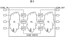
まず、ロジックBISTで行うスキャンテストについて図1から図3を用いて説明する。
図1はマルチプレクサ方式のスキャン用フリップフロップの構成を示す図である。図2はスキャンテストの構成を示す図である。図3はスキャンテストのタイミングを示す図である。
スキャンテストは、テストを容易にする設計手法であるDFT(Design for Testability)技術の一つで、AND回路、OR回路、インバータ、フリップフロップなどの論理回路を組み合わせて所定の論理機能を構成したランダムロジックを対象にする。図1に示すように、スキャンテストでは、回路内のフリップフロップ(FF)をスキャン用フリップフロップ(SFF)に置き換える。マルチプレクサ方式のスキャン用フリップフロップは、マルチプレクサ(MUX)と通常のフリップフロップ(FF)で構成される。スキャンイネーブル(SE)信号で通常動作とテストモード動作を切り替える。図2に示すように、テストモード時には回路内のスキャン用フリップフロップをシリアルに接続することでシフトレジスタを形成し、スキャンテスト対象ブロックの入出力端子からスキャン用フリップフロップを制御・観測できるような経路(スキャンチェーン(SCAN CHAIN))を設ける。
このような構成を採ると、スキャン用フリップフロップがスキャンテスト対象ブロックの入出力端子と等価と見なせるため、テストの対象は組み合わせ回路(CL)のみとなる。組み合わせ回路(CL)に対してのテストパターン生成技術はATPG(Automatic Test Pattern Generation)として確立しており、効率良くテストパターンを自動生成できることになる。
First, a scan test performed by the logic BIST will be described with reference to FIGS.
FIG. 1 is a diagram showing a configuration of a multiplexer-type scan flip-flop. FIG. 2 is a diagram showing the configuration of the scan test. FIG. 3 is a diagram showing the timing of the scan test.
Scan test is one of DFT (Design for Testability) technology that is a design method that facilitates the test. Random is a combination of AND circuits, OR circuits, inverters, flip-flops and other logic circuits that form a predetermined logic function. Target logic. As shown in FIG. 1, in the scan test, the flip-flop (FF) in the circuit is replaced with a scan flip-flop (SFF). A multiplexer-type scan flip-flop is composed of a multiplexer (MUX) and a normal flip-flop (FF). A normal operation and a test mode operation are switched by a scan enable (SE) signal. As shown in FIG. 2, in the test mode, the scan flip-flops in the circuit are serially connected to form a shift register so that the scan flip-flops can be controlled and observed from the input / output terminals of the scan test target block. Establish a route (scan chain (SCAN CHAIN)).
When such a configuration is adopted, the scan flip-flop can be regarded as equivalent to the input / output terminal of the scan test target block, so that the test target is only the combinational circuit (CL). A test pattern generation technique for the combinational circuit (CL) has been established as ATPG (Automatic Test Pattern Generation), and a test pattern can be automatically generated efficiently.
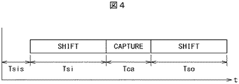
スキャンテストは、図3に示すように、スキャンイン(SCAN IN)→キャプチャ(CAPTURE)→スキャンアウト(SCAN OUT)という一連の動作を複数回繰り返して進められる。
まず、スキャンイネーブル信号でスキャンモードに設定し、スキャンイン端子(SCAN_IN)からスキャン用フリップフロップに対してテストパターンを設定する。次に、スキャンイネーブル信号で通常動作モードに設定し、スキャン用フリップフロップ間の組み合わせ回路を動作させる。そして、テストクロックを動作させて、組み合わせ回路の出力をスキャン用フリップフロップに取り込む。その次に、再びスキャンイネーブル信号でスキャンモードに設定し、スキャン用フリップフロップに取り込んだ値をスキャンアウト端子(SCAN_OUT)で観測する。
最初のスキャンインではスキャンモードになり、スキャンイン端子からスキャン用フリップフロップにテストパターンを送り込む。シリアルに入力するため、全スキャン用フリップフロップへの設定はスキャン用フリップフロップ数回のシフト動作(スキャン用フリップフロップ数クロック)が必要である。
次のキャプチャでは通常動作モードになり、スキャン用フリップフロップ間の組み合わせ回路を動作させる。そして、組み合わせ回路の出力をスキャン用フリップフロップ(SFF)に取り込む。
3番目のスキャンアウトでは、再びスキャンモードになる。スキャン用フリップフロップに格納してある値をスキャンアウト端子で観測する。この観測した値を、あらかじめ求めてある期待値(故障がない場合の値)と比較し、故障の有無を判定する。なおスキャンアウトもシリアルな出力のため、全スキャン用フリップフロップからの値の読みだしにはスキャン用フリップフロップ数のシフト動作(スキャン用フリップフロップ数のクロック数)が必要となる。
As shown in FIG. 3, the scan test is performed by repeating a series of operations of scan-in (SCAN IN) → capture (CAPTURE) → scan-out (SCAN OUT) a plurality of times.
First, the scan mode is set by the scan enable signal, and the test pattern is set from the scan-in terminal (SCAN_IN) to the scan flip-flop. Next, the normal operation mode is set by the scan enable signal, and the combinational circuit between the scan flip-flops is operated. Then, the test clock is operated to take the output of the combinational circuit into the scan flip-flop. Next, the scan mode is set again by the scan enable signal, and the value taken into the scan flip-flop is observed at the scan-out terminal (SCAN_OUT).
In the first scan-in, the scan mode is set, and a test pattern is sent from the scan-in terminal to the scan flip-flop. In order to input serially, setting to all the flip-flops for scanning requires a shift operation (several clocks for the number of flip-flops for scanning) several times.
At the next capture, the normal operation mode is set, and the combinational circuit between the scan flip-flops is operated. Then, the output of the combinational circuit is taken into a scan flip-flop (SFF).
In the third scan-out, the scan mode is entered again. The value stored in the scan flip-flop is observed at the scan-out terminal. The observed value is compared with an expected value obtained in advance (a value when there is no failure) to determine whether or not there is a failure. Since the scan-out is also a serial output, a shift operation of the number of scan flip-flops (the number of clocks of the number of scan flip-flops) is required for reading values from all the scan flip-flops.
スキャンインおよびスキャンアウトのシフト動作は消費電流が大きく、キャプチャは消費電流が小さい。また、複数のBISTを並列に動作させた場合、スキャンインおよびスキャンアウトのシフト動作は消費電流がさらに大きくなる。この結果、スキャンインおよびスキャンアウトのシフト動作とキャプチャとの間の消費電流の変動率が大きくなると、電源ラインに共振ノイズが発生する可能性が高まる。 The scan-in and scan-out shift operations consume a large amount of current, and the capture consumes a small amount of current. When a plurality of BISTs are operated in parallel, the scan-in and scan-out shift operations further consume current. As a result, when the fluctuation rate of the current consumption between the scan-in and scan-out shift operations and capture increases, the possibility of resonance noise occurring in the power supply line increases.
<実施形態>
次に、実施形態に係る半導体装置について図4および図5を用いて説明する。
図4は実施形態に係る半導体装置のスキャンテストのタイミングを説明するための図である。図5は実施形態に係る半導体装置の効果を説明するためのタイミング図である。
上述したように、スキャンテストはスキャンインのシフト動作とキャプチャとスキャンアウトのシフト動作を有する。
スキャンインを開始する遅れ期間(Tsis)、スキャンイン期間(Tsi)、キャプチャ期間(Tca)、スキャンアウト期間(Tso)を可変とする。スキャンインを開始する遅れ期間(Tsis)はスキャンテストを起動してからスキャンインを開始するまでの時間を可変にしてよいし、スキャンテストの起動時間を可変にしてもよい。スキャンシフト長(スキャンチェーン段数)をn、スキャンクロック周波数をfs(スキャンクロック周期をTs)とすると、
Tsi=Tso=n×1/fs=n×Ts
であるので、スキャンチェーン段数(n)およびスキャンクロック周波数(fs)の少なくともいずれか1つを変えることにより、スキャンイン期間(Tsi)およびスキャンアウト期間(Tso)を変えることができる。スキャンチェーンの構成を変えることによりスキャンチェーン段数(n)を変えることができる。
キャプチャクロックは、スキャン用フリップフロップに取り込むため、1回High(ハイ)が出力されるので、キャプチャクロックがHighになる前のLow(ロウ)の期間やHighになった後のLowの期間(次のスキャンクロックがHighになる前のLowの期間)を変えることによりキャプチャ期間(Tca)を変えることができる。
<Embodiment>
Next, the semiconductor device according to the embodiment will be described with reference to FIGS.
FIG. 4 is a diagram for explaining the scan test timing of the semiconductor device according to the embodiment. FIG. 5 is a timing chart for explaining the effect of the semiconductor device according to the embodiment.
As described above, the scan test has a scan-in shift operation and a capture / scan-out shift operation.
The delay period (Tsis) for starting the scan-in, the scan-in period (Tsi), the capture period (Tca), and the scan-out period (Tso) are variable. In the delay period (Tsis) for starting the scan-in, the time from the start of the scan test to the start of the scan-in may be made variable, or the start time of the scan test may be made variable. When the scan shift length (number of scan chain stages) is n and the scan clock frequency is fs (scan clock cycle is Ts),
Tsi = Tso = n × 1 / fs = n × Ts
Therefore, the scan-in period (Tsi) and the scan-out period (Tso) can be changed by changing at least one of the number of scan chain stages (n) and the scan clock frequency (fs). The number of scan chain stages (n) can be changed by changing the configuration of the scan chain.
Since the capture clock is captured by the scan flip-flop, High (High) is output once. Therefore, the Low period before the capture clock becomes High or the Low period after the Capture clock becomes High (next) The capture period (Tca) can be changed by changing the Low period before the scan clock becomes high.
実施形態に係る半導体装置はBISTを行うためのスキャン回路を備え、スキャンインの期間、スキャンアウトの期間およびキャプチャの期間の長さの少なくとも1つが変更可能とされ、かつスキャン動作開始時期を変更可能とされる。
例えば、図5に示すように、2つのBISTが並列に動作する場合、1つ目のBISTのスキャンインを開始する時間(Tsis1)と2つ目のBISTのスキャンインを開始する時間(Tsis2)を変えて設定することにより、消費電流の小さいキャプチャと消費電流の大きいシフト動作が並列して動作することが可能となる。これにより、消費電流の変動率が低減し、電源ラインの共振ノイズの発生を低減することが可能となる。ここで、2つのBISTのスキャンイン期間(Tsi)、キャプチャ期間(Tca)、スキャンアウト期間(Tso)を合わせるのが好ましい。2つのBISTが並列に動作する場合に限定されるものではなく、3つ以上のBISTが並列に動作する場合にも適用できる。複数のBISTは同一半導体装置内で行われてもよいし、異なる半導体装置で行われてもよい。
The semiconductor device according to the embodiment includes a scan circuit for performing BIST, and at least one of the length of the scan-in period, the scan-out period, and the capture period can be changed, and the scan operation start timing can be changed It is said.
For example, as shown in FIG. 5, when two BISTs operate in parallel, the time for starting the first BIST scan-in (Tsis1) and the time for starting the second BIST scan-in (Tsis2) By changing the setting, it is possible to perform a capture operation with a small current consumption and a shift operation with a large current consumption in parallel. As a result, the fluctuation rate of the current consumption is reduced, and the generation of resonance noise in the power supply line can be reduced. Here, it is preferable to combine the scan-in period (Tsi), the capture period (Tca), and the scan-out period (Tso) of the two BISTs. The present invention is not limited to the case where two BISTs operate in parallel, and can also be applied to a case where three or more BISTs operate in parallel. The plurality of BISTs may be performed in the same semiconductor device or may be performed in different semiconductor devices.
次に、実施例に係るマイクロコントローラの構成について図6を用いて説明する。
図6は実施例に係るマイクロコントローラの構成を示すブロック図である。
実施例に係るマイクロコントローラ1は、ロジック部の自己診断(ロジックBIST)機能とメモリ部の自己診断(メモリBIST)機能とを備え、ロジックBIST回路10と、スキャン対象回路20と、スキャン非対称回路30とを一つの半導体基板に備える半導体装置である。
ロジックBIST回路10は、BIST制御回路(BIST CONTROL:BC)11と、チェーン制御回路(CHAIN CONTROL)12と、クロック制御回路(CLOCK CONTROL)13と、リセット制御回路(RESET CONTROL)14と、パターン生成回路(PATTERN GENERATOR:PG)15と、を備える。ロジックBIST回路10は、さらに、スキャン許可制御回路(SCAN ENABLE CONTROL:SEC)16と、圧縮回路(COMPRESS)17と、比較結果状態回路(RESULT COMPARE STATUS:RCS)18と、電気的に書換可能な不揮発性メモリであるフラッシュメモリ19と、を備える。
スキャン対象回路20は、中央処理装置(CPU)21と、ダイレクト・メモリ・アクセス制御装置(DMA)と、タイマ(TIMER)と、PWM生成回路(PWM)と、通信回路であるコントローラ・エリア・ネットワーク(Controller Area Network:CAN)と、A/D変換回路(ADC)と、シリアル・ペリフェラル・インタフェース(SPI)と、等のMCUの各機能ブロックを備える。スキャン対象回路20は、さらに、メモリBIST制御回路(MEMORY BIST CONTROL:MBC)22と、メモリパターン生成回路(MEMORY PATTERN GENERATOR:MPG)23と、メモリBIST結果チェック回路(MEMORY BIST RESULT CHECK:MBRC)24と、等のメモリBIST回路を備える。これにより、メモリBIST回路のスキャンテストを行うことができる。
スキャン非対象回路30は、メモリであるSRAM31とアナログ回路(ANALOG H/M)32である。なお、CPU21が実行するプログラムやデータはフラッシュメモリ19に格納される。プログラムや後述するパラメータは半導体装置の製造後にフラッシュメモリ19に書き込まれる。
Next, the configuration of the microcontroller according to the embodiment will be described with reference to FIG.
FIG. 6 is a block diagram illustrating the configuration of the microcontroller according to the embodiment.
The
The
The
The scan
次に、マイクロコントローラ1のBIST動作について図7および図8を用いて説明する。
図7は実施例に係るマイクロコントローラのスキャンテスト前までのBIST動作を説明するためのブロック図である。図8は実施例に係るマイクロコントローラのスキャンテスト後のBIST動作を説明するためのブロック図である。
リセット解除後、BIST制御回路11がフラッシュメモリ19からパラメータを読出して、チェーン制御回路12、クロック制御回路13、リセット制御回路14、パターン生成回路15、スキャン許可制御回路16にパラメータを展開する。リセット解除後所定時間経過後スキャンテストを開始する。例えば、後述するスキャンクロックをスキャン対象回路20に供給開始することによりスキャンテストを開始するようする。
チェーン制御回路12は、BIST制御回路11から与えられるパラメータにより、スキャンテスト対象回路20のスキャンチェーンの構成を設定するものである。詳細は後述する。
クロック制御回路13は、BIST制御回路11から与えられるパラメータにより、スキャンテスト実行時のスキャンクロック、キャプチャクロックを制御するものである。スキャンクロックの供給開始時期の設定により、スキャン開始遅れ時間が変更可能となる。例えば、クロックスキャンをカウンタで計数し、所定のスキャンクロック数後に、スキャンクロックをスキャンチェーンに供給するようにする。また、スキャンクロックの周波数やキャプチャクロックのLowの期間が設定され、スキャンイン期間およびスキャンアウト期間、キャプチャ期間が変更可能となる。BISTは、スキャンイン、キャプチャ、スキャンアウトで構成されるスキャンテストが複数回繰り返されるが、n番目のスキャンテストと(n+1)番目のスキャンテストの間の期間を設定することもできる。これらにより、複数の半導体装置のBISTの並列動作の他に、時分割動作も可能となる。
リセット制御回路14はスキャンチェーンを構成するフリップフロップのセットまたはリセットを制御するものであり、スキャンテスト中にフリップフロップが予期しない値にならないようにするものである。
パターン生成回路15は、BIST制御回路11から与えられるパラメータにより、スキャンチェーン構成に合わせて、スキャンテスト用のパターンを生成する。圧縮回路17はスキャンテスト結果を論理圧縮する。
Next, the BIST operation of the
FIG. 7 is a block diagram for explaining the BIST operation before the scan test of the microcontroller according to the embodiment. FIG. 8 is a block diagram for explaining the BIST operation after the scan test of the microcontroller according to the embodiment.
After releasing the reset, the
The
The
The
The
スキャンテスト後、結果を圧縮回路17で圧縮し、比較結果状態回路18に格納する。メモリBIST制御回路22の制御に基づいてSRAM31のメモリテストを実施し、結果を比較結果状態回路18に格納する。CPU21が通常動作を開始し、フラッシュメモリ19に格納されている期待値を比較結果状態回路18に書込む。比較結果状態回路18が期待値とテスト結果とを比較しその結果を保持する。CPU21が比較結果状態回路18から比較結果を読み出して判定を行う。CPU21がBISTの一部を実施することにより、比較結果回路18のハードフェア規模の増大を抑えることができる。
After the scan test, the result is compressed by the
次に、スキャンテスト対象ブロックの内部構成について図9および図1を用いて説明する。
図9は実施例に係るマイクロコントローラのスキャンテスト対象ブロックの内部構成を説明するためのブロック図である。
スキャンチェーンは横方向に構成されており、図面左側からテスト信号である第1から第3のスキャンイン信号(SIN1,SIN2,SIN3)が入力され、図面右側に第1から第3のスキャンアウト信号(OUT1,OUT2,OUT3)が出力される。図1に示すように、スキャン用フリップフロップ(SFF)はフリップフロップ(FF)のデータ入力端子(D)にマルチプレクサ(MUX)が接続されている。マルチプレクサ(MUX)はスキャンイネーブル信号(SE)に基づいて組み合わせ回路の出力信号(IN_CL)とスキャンチェーン前段のスキャン用フリップフロップの出力信号(SCn−1)とを切り替えてフリップフロップ(FF)のデータ入力端子(D)に入力する。スキャン用フリップフロップ(SFF)(フリップフロップ(FF))にはスキャンクロック信号(CLK)が入力される。破線部分はテスト用回路以外の通常論理(組み合わせ回路)CLC1〜CLC4であり、スキャンチェーン順に関係なく接続されて存在する。各スキャン用フリップフロップ(SFFn)はスキャンチェーンで接続され、スキャンチェーンによる各スキャン用フリップフロップの値のセット(スキャンイン)、読み出し(スキャンアウト)により、組み合わせ回路のテストが行われる。さらに、本実施例のスキャンチェーンでは、その構成を変更可能とするためのセレクタSEL1〜SEL6が配置される。BIST制御回路11から与えられるパラメータにより、セレクタSEL1〜SEL6が設定され、スキャンチェーンの構成が決まる。
Next, the internal configuration of the scan test target block will be described with reference to FIGS.
FIG. 9 is a block diagram for explaining the internal configuration of the scan test target block of the microcontroller according to the embodiment.
The scan chain is configured in a horizontal direction, and first to third scan-in signals (SIN1, SIN2, SIN3) as test signals are input from the left side of the drawing, and first to third scan-out signals are input to the right side of the drawing. (OUT1, OUT2, OUT3) is output. As shown in FIG. 1, the scan flip-flop (SFF) has a multiplexer (MUX) connected to the data input terminal (D) of the flip-flop (FF). Based on the scan enable signal (SE), the multiplexer (MUX) switches between the output signal (IN_CL) of the combinational circuit and the output signal (SCn-1) of the scan flip-flop in the previous stage of the scan chain, and the data of the flip-flop (FF) Input to the input terminal (D). A scan clock signal (CLK) is input to the scan flip-flop (SFF) (flip-flop (FF)). The broken line portions are normal logic (combination circuits) CLC1 to CLC4 other than the test circuit, and are connected regardless of the scan chain order. Each scan flip-flop (SFFn) is connected by a scan chain, and the combinational circuit is tested by setting (scanning in) and reading (scanout) the value of each scan flip-flop by the scan chain. Furthermore, in the scan chain of the present embodiment, selectors SEL1 to SEL6 are arranged for making the configuration changeable. The selectors SEL1 to SEL6 are set according to the parameters given from the
次に、スキャンチェーンの第1の構成例について図10を用いて説明する。図10は実施例に係るマイクロコントローラのスキャンチェーンの第1の構成例を示すブロック図である。
スキャンチェーンの第1の構成例では、BIST制御回路11与えられたパラメータが、各セレクタについて、以下の信号を選択するようになっている。
セレクタSEL1:第1のスキャンイン信号(SIN1)
セレクタSEL2:第2のスキャンイン信号(SIN2)
セレクタSEL3:第3のスキャンイン信号(SIN3)
セレクタSEL4:第100のスキャン用フリップフロップ(SFF100)の出力信号
セレクタSEL5:第150のスキャン用フリップフロップ(SFF150)の出力信号
セレクタSEL6:第300のスキャン用フリップフロップ(SFF300)の出力信号
この場合、スキャンチェーンの第1の構成例は、以下の3つのスキャンチェーン構成となる。
チェーンCH11:SIN1,SFF1,SFF2,・・・,SFF100,OUT1
チェーンCH12:SIN2,SFF101,・・・,SFF200,OUT2
チェーンCH13:SIN3,SFF201,・・・,SFF300,OUT3
チェーンCH11,CH12,CH13の段数はそれぞれ100段となる。
Next, a first configuration example of the scan chain will be described with reference to FIG. FIG. 10 is a block diagram illustrating a first configuration example of the scan chain of the microcontroller according to the embodiment.
In the first configuration example of the scan chain, the parameters given to the
Selector SEL1: first scan-in signal (SIN1)
Selector SEL2: second scan-in signal (SIN2)
Selector SEL3: third scan-in signal (SIN3)
Selector SEL4: Output signal of 100th scan flip-flop (SFF100) Selector SEL5: Output signal of 150th scan flip-flop (SFF150) Selector SEL6: Output signal of 300th scan flip-flop (SFF300) In this case The first configuration example of the scan chain has the following three scan chain configurations.
Chain CH11: SIN1, SFF1, SFF2, ..., SFF100, OUT1
Chain CH12: SIN2, SFF101, ..., SFF200, OUT2
Chain CH13: SIN3, SFF201, ..., SFF300, OUT3
Each of the chains CH11, CH12, and CH13 has 100 stages.
次に、スキャンチェーンの第2の構成例について図11を用いて説明する。図11は実施例に係るマイクロコントローラのスキャンチェーンの第2の構成例を示すブロック図である。
スキャンチェーンの第2の構成例では、BIST制御回路11与えられたパラメータが、各セレクタについて、以下の信号を選択するようになっている。
セレクタSEL1:第1のスキャンイン信号(SIN1)
セレクタSEL2:第300のスキャン用フリップフロップ(SFF300)の出力信号
セレクタSEL3:第3のスキャンイン信号SIN3
セレクタSEL4:第200のスキャン用フリップフロップSFF200の出力信号
セレクタSEL5:第100のスキャン用フリップフロップSFF100の出力信号
セレクタSEL6:第150のスキャン用フリップフロップSFF150の出力信号
この場合、スキャンチェーンの第2の構成例は、以下の2つのスキャンチェーン構成となる。
チェーンCH21:SIN1,SFF1,SFF2,・・・,
SFF100,SFF151,・・・,SFF200,OUT1
チェーンCH22:SIN3,SFF201,・・・,
SFF300,SFF101,・・・,SFF150,OUT3
チェーンCH21,CH22の段数はそれぞれ150段となる。
Next, a second configuration example of the scan chain will be described with reference to FIG. FIG. 11 is a block diagram illustrating a second configuration example of the scan chain of the microcontroller according to the embodiment.
In the second configuration example of the scan chain, the parameters given to the
Selector SEL1: first scan-in signal (SIN1)
Selector SEL2: Output signal of 300th scan flip-flop (SFF300) Selector SEL3: Third scan-in signal SIN3
Selector SEL4: Output signal of the 200th scan flip-flop SFF200 Selector SEL5: Output signal of the 100th scan flip-flop SFF100 Selector SEL6: Output signal of the 150th scan flip-flop SFF150 In this case, the second signal of the scan chain This configuration example has the following two scan chain configurations.
Chain CH21: SIN1, SFF1, SFF2, ...,
SFF100, SFF151, ..., SFF200, OUT1
Chain CH22: SIN3, SFF201, ...
SFF300, SFF101, ..., SFF150, OUT3
Each of the chains CH21 and CH22 has 150 stages.
実施例によれば、スキャンチェーンの構成を半導体装置の製造後に変更することが可能である。スキャンチェーンの構成、すなわちスキャンチェーンの段数が変更可能となることのより、スキャンイン期間およびスキャンアウト期間の長さを変更可能となる。また、キャプチャ期間の長さが半導体装置の製造後に変更可能である。これらにより、異なる半導体間でスキャンテスト期間を合わせることが可能となる。また、スキャン開始時期が半導体装置の製造後に変更可能である。これにより、異なる半導体間でスキャンテスト期間すなわち消費電流が大きいシフト動作と消費電流の小さいキャプチャとを並行して実施することが可能となり、消費電流の変動率の低減が可能となる。 According to the embodiment, the configuration of the scan chain can be changed after the semiconductor device is manufactured. Since the configuration of the scan chain, that is, the number of stages of the scan chain can be changed, the length of the scan-in period and the scan-out period can be changed. Further, the length of the capture period can be changed after manufacturing the semiconductor device. As a result, the scan test periods can be matched between different semiconductors. The scan start time can be changed after the semiconductor device is manufactured. As a result, a scan test period, that is, a shift operation with a large current consumption and a capture with a small current consumption can be performed in parallel between different semiconductors, and the fluctuation rate of the current consumption can be reduced.
<応用例1>
次にBISTを内蔵したマイクロコントローラを用いた第1の応用例(応用例1)に係る電子装置について図12を用いて説明する。図12は応用例1に係る電子装置の構成を示すブロック図である。
応用例1に係る電子装置101は、第1の半導体装置であるマイクロコントローラ(MCU)1Aと、第2の半導体装置であるマイクロコントローラ(MCU)1Bと、電源IC(POWER)2と、受動素子(PE)3と、を1つまたは複数のプリント基板上に備える。電源IC2と、マイクロコントローラ1A,1Bおよび受動素子3と、の間の電源線およびグラウンド線にはインダクタンスL1〜L7やキャパシタンスCの成分を含む。電子装置101は、例えば自動車のエンジン制御、ブレーキ制御等の各種車載制御に用いられるECU(Electronics Control Unit)である。
<Application example 1>
Next, an electronic device according to a first application example (application example 1) using a microcontroller incorporating BIST will be described with reference to FIG. FIG. 12 is a block diagram illustrating a configuration of an electronic device according to Application Example 1.
The
マイクロコントローラ1A,1Bは実施例に係るマイクロコントローラ1と同様な構成である。マイクロコントローラ1A,1BのBISTのパラメータを下記のように設定する。
(1)マイクロコントローラ1A,1Bのスキャンチェーン構成が同じになるように、パラメータをマイクロコントローラ1A、1Bの各フラッシュメモリに書き込む。すなわち、例えば、実施例のスキャンチェーンの第1の構成例(または第2の構成例)のパラメータをセットする。
(2)マイクロコントローラ1A,1Bのスキャンテストの起動タイミングをずらすようにする。より具体的には、マイクロコントローラ1Aのシフト動作中にマイクロコントローラ1Bのキャプチャ動作が行われ、マイクロコントローラ1Bのシフト動作中にマイクロコントローラ1Aのキャプチャ動作中が行われるようにする。例えば、マイクロコントローラ1Aのスキャンインのシフト動作が完了してから、マイクロコントローラ1Bのスキャンインのシフト動作を開始する。このとき、マイクロコントローラ1Aのスキャンイン期間、キャプチャ期間およびスキャンアウト期間のスキャンテスト期間とマイクロコントローラ1Bのスキャンテスト期間とが同等な期間とする。そうすると、マイクロコントローラ1Aのキャプチャ動作とマイクロコントローラ1Bのスキャンイン動作とが並行して行われ、マイクロコントローラ1Aのスキャンアウト動作とマイクロコントローラ1Bのキャプチャ動作とが並行して行われ、マイクロコントローラ1Aのスキャンイン動作とマイクロコントローラ1Bのキャプチャ動作とが並行して行われる。これにより、消費電流の変動率を低減することができ、電源共振ノイズを低減することが可能となる。
マイクロコントローラ1A,1Bが異なる種類のマイクロコントローラである場合、例えば、マイクロコントローラ1Aのスキャンチェーンが可変構成となっておらず、150段で固定であった場合は、マイクロコントローラ1Bのスキャンチェーンを第2の構成例とすればよい。
The
(1) Parameters are written in the flash memories of the
(2) The start timing of the scan test of the
When the
<応用例2>
次にBISTを内蔵したマイクロコントローラを用いた第2の応用例(応用例2)に係る電子装置について図13から図15を用いて説明する。図13は応用例2に係る電子装置の構成を示すブロック図である。図14は応用例2に係る電子装置の第1の動作を示すブロック図である。図15は応用例2に係る電子装置の第2の動作を示すブロック図である。
応用例2に係る電子装置102はマスタ側の半導体装置(LSI)1Mと、スレーブ側の半導体装置(LSI)1S1と、スレーブ側の半導体装置(LSI)1S2と、電源IC2と、受動素子3と、を1つまたは複数のプリント基板上に備える。電源IC2と、半導体装置1M、1S1、1S2および受動素子PEと、の間の電源線およびグラウンド線にはインダクタンスL1〜L9やキャパシタンスC成分を含む。電子装置102は、電子装置101と同様に、例えば自動車のエンジン制御、ブレーキ制御等の各種車載制御に用いられるECU(Electronics Control Unit)である。
半導体装置1M,1S1,1S2は非スキャン対象回路に電源電圧監視用A/D変換回路33を備えることを除き、実施例に係るマイクロコントローラ1と同様な構成である。半導体装置1Mを第1の半導体装置といい、半導体装置1S1,1S2のいずれかを第2の半導体装置ということもある。
<Application example 2>
Next, an electronic apparatus according to a second application example (application example 2) using a microcontroller incorporating BIST will be described with reference to FIGS. FIG. 13 is a block diagram illustrating a configuration of an electronic apparatus according to Application Example 2. FIG. 14 is a block diagram illustrating a first operation of the electronic apparatus according to the application example 2. FIG. 15 is a block diagram illustrating a second operation of the electronic device according to the application example 2.
The
The
応用例2に係る電子装置の第1の動作について図14を用いて説明する。
(A1)半導体装置1Mの電源電圧監視用A/D変換回路33はスキャンテスト中のインダクタンスL2とインダクタンスL4との間の電源電圧を監視する。同様に、半導体装置1S1の電源電圧監視用A/Dコンバータ33はスキャンテスト中のそれぞれインダクタンスL4とインダクタンスL6との間の電源電圧を監視する。半導体装置1S2の電源電圧監視用A/Dコンバータ33はスキャンテスト中のインダクタンスL6とインダクタンスL8との間の電源電圧を監視する。
(A2)スキャンテスト後、スレーブ側の半導体装置1S1,1S2はそれぞれ電源電圧の変動をマスタ側の半導体装置1MへCANなどで転送する。
(A3)マスタ側の半導体装置1Mにてパラメータを再計算し、各スレーブ側の半導体装置1S1,1S2へ新パラメータを連絡する。電源電圧の変動が閾値を超えているような場合は、共振が発生していると判断し、スキャンチェーンの構成を変更する。例えば、マスタ側の半導体装置1Mのスキャンチェーンの段数を増やす、あるいは減らすようにパラメータを変更する。
(A4)次回からのBIST実行時には上記(A3)で変更した新パラメータにて実行する。
応用例2の第1の動作によれば、実際の電源電圧の変動をモニタすることにより、応用例1よりも電源共振ノイズを低減することが可能となる。
A first operation of the electronic device according to Application Example 2 will be described with reference to FIG.
(A1) The power supply voltage monitoring A /
(A2) After the scan test, each of the slave-side semiconductor devices 1S1 and 1S2 transfers the fluctuation of the power supply voltage to the master-
(A3) The parameters are recalculated in the
(A4) At the next BIST execution, the new parameters changed in the above (A3) are executed.
According to the first operation of the application example 2, it is possible to reduce the power supply resonance noise compared to the application example 1 by monitoring the actual fluctuation of the power supply voltage.
応用例2に係る電子装置の第2の動作について図15を用いて説明する。
(B1)上記(A1)と同様にスキャンテスト中に各半導体装置1M,1S1,1S2の電源電圧を電源電圧監視用A/D変換回路33にて監視する。
(B2)上記(A2)と同様に上記(B2)で検出した電源電圧の変動をマスタ側の半導体装置1MへCANなどで転送する。
(B3)マスタ側の半導体装置1Mにてパラメータを再計算する。このとき、受動素子3に流れる異常電流分を加味しパラメータ再設定する。電源IC2の容量超過の場合はBISTの並列動作から時分割動作などに移行し、状態エラーを通知する。これにより、電源の容量超過の場合でもBISTの実行が可能となる。
受動素子3に短絡等の故障が発生した場合、受動素子3で電源−グラウンド間に定常的に異常電流(Iab)が流れる。このとき、3つの半導体装置1M,1S1,1S2は、電源IC2から供給される電流のうち、異常電流(Iab)を差し引いたものを使用することになるため、通常時よりも使用可能な動作電流が少なくなる。よって、素子故障を検出した場合は、スキャンチェーンの構成(スキャンチェーンの段数)設定に加え、更に3つの半導体装置1M,1S1,1S2それぞれのスキャンクロックの周波数を故障が無い場合よりも低くなるように設定する。これにより、受動素子の故障等により電源の使用可能な動作電流が少なくなった場合でもBISTの実行が可能となる。
A second operation of the electronic device according to the application example 2 will be described with reference to FIG.
(B1) The power supply voltage of each of the
(B2) Similarly to (A2), the fluctuation of the power supply voltage detected in (B2) is transferred to the master-
(B3) The parameter is recalculated in the
When a failure such as a short circuit occurs in the
以上、本発明者によってなされた発明を実施形態、実施例および応用例に基づき具体的に説明したが、本発明は、上記実施形態、実施例および応用例に限定されるものではなく、種々変更可能であることはいうまでもない。 As mentioned above, the invention made by the present inventor has been specifically described based on the embodiments, examples, and application examples. However, the present invention is not limited to the above-described embodiments, examples, and application examples, and various modifications are made. It goes without saying that it is possible.
1 ・・・マイクロコントローラ(半導体装置)
10 ・・・自己診断関連回路
11 ・・・BIST制御部
12 ・・・チェーン制御部
13 ・・・クロック制御部
14 ・・・リセット制御部
15 ・・・パターン生成部
16 ・・・スキャン許可制御部
17 ・・・圧縮部
18 ・・・比較結果状態部
19 ・・・フラッシュメモリ
20 ・・・スキャン対象回路
21 ・・・CPU
22 ・・・メモリBIST制御部
23 ・・・メモリパターン生成部
24 ・・・メモリBIST結果チェック部
30 ・・・スキャン非対象回路
31 ・・・SRAM
32 ・・・アナログ部
33 ・・・電源電圧監視用A/D変換回路
101 ・・・電子装置
1A,1B ・・・マイクロコントローラ(半導体装置)
2 ・・・電源IC
102 ・・・電子装置
1M ・・・マスタ側の半導体装置
1S1,1S2・・・スレーブ側の半導体装置
1 ... Microcontroller (semiconductor device)
DESCRIPTION OF
22 ... Memory
32...
2 ... Power supply IC
102:
Claims (17)
スキャン対象回路と、
電気的に書き換え可能な不揮発性メモリと、
を備え、
前記スキャン対象回路は、
組合せ回路と、
スキャン用フリップフロップと、
を備え、
前記スキャン用フリップフロップを複数段接続してスキャンチェーンを構成するようにされ、
前記自己診断制御回路は、前記不揮発性メモリに格納されるパラメータに従って、前記スキャンチェーンにテストデータを入力するスキャンインの期間、前記スキャンチェーンからテスト結果を出力するスキャンアウトの期間および前記組合せ回路のテスト結果を前記スキャンチェーンに取り込むキャプチャの期間の長さの少なくとも1つが変更可能とされ、かつスキャン動作開始時期を変更可能とされる半導体装置。 A self-diagnosis control circuit;
A circuit to be scanned;
An electrically rewritable nonvolatile memory;
With
The circuit to be scanned is
A combinational circuit;
A flip-flop for scanning;
With
A plurality of stages of the scan flip-flops are connected to form a scan chain,
The self-diagnosis control circuit includes a scan-in period in which test data is input to the scan chain, a scan-out period in which a test result is output from the scan chain, and a combination circuit according to parameters stored in the nonvolatile memory. A semiconductor device in which at least one of the lengths of a capture period for taking a test result into the scan chain can be changed, and the scan operation start time can be changed.
スキャンチェーン制御回路を備え、
前記スキャン対象回路は、複数のスキャン用フリップフロップの出力を切り替えるセレクタを備え、
前記スキャンチェーン制御回路は、前記不揮発性メモリに格納されるパラメータに従って、前記セレクタを制御することにより、スキャンチェーン構成を変更可能とされる半導体装置。 The semiconductor device according to claim 1, further comprising a scan chain control circuit,
The scan target circuit includes a selector that switches the outputs of a plurality of scan flip-flops,
The scan chain control circuit is a semiconductor device in which a scan chain configuration can be changed by controlling the selector according to a parameter stored in the nonvolatile memory.
前記スキャン対象回路は並列に動作する複数のスキャンチェーンを含む半導体装置。 The semiconductor device according to claim 2.
The scan target circuit includes a plurality of scan chains operating in parallel.
前記スキャンチェーンのスキャン用フリップフロップの接続段数を変更可能とされる半導体装置。 The semiconductor device according to claim 2.
A semiconductor device capable of changing the number of connection stages of scan flip-flops of the scan chain.
クロック制御回路を備え、
前記クロック制御回路は、前記不揮発性メモリに格納されるパラメータに従って、前記スキャンチェーンのシフトクロックの周波数を変更可能とされる半導体装置。 2. The semiconductor device according to claim 1, further comprising:
With clock control circuit,
The semiconductor device in which the clock control circuit can change the frequency of the shift clock of the scan chain in accordance with parameters stored in the nonvolatile memory.
クロック制御回路を備え、
前記クロック制御回路は、前記不揮発性メモリに格納されるパラメータに従って、前記組合せ回路のテスト結果を前記スキャンチェーンに取り込むキャプチャクロックのLow期間を変更可能とされる半導体装置。 The semiconductor device according to claim 1.
With clock control circuit,
The semiconductor device in which the clock control circuit is capable of changing a low period of a capture clock for capturing a test result of the combinational circuit into the scan chain according to a parameter stored in the nonvolatile memory.
テストデータを生成するパターン生成回路と、
スキャンテスト結果を圧縮する圧縮回路と、
圧縮結果を格納する比較結果状態回路と、
を備え、
スキャンテストの期待値を不揮発性メモリに格納する半導体装置。 The semiconductor device according to claim 1.
A pattern generation circuit for generating test data;
A compression circuit for compressing the scan test results;
A comparison result state circuit for storing the compression result; and
With
A semiconductor device that stores an expected value of a scan test in a nonvolatile memory.
前記スキャン対象回路はCPUを備え、
前記CPUが前記不揮発性メモリに格納されるスキャン期待値を前記回路に書き込むことにより、前記回路はスキャンテスト結果と前記スキャン期待値とを比較する半導体装置。 The semiconductor device according to claim 7.
The scan target circuit includes a CPU,
A semiconductor device in which the CPU writes a scan expected value stored in the nonvolatile memory into the circuit, so that the circuit compares a scan test result with the scan expected value.
メモリを含むスキャン非対象回路と、
前記メモリを自己診断するメモリ自己診断回路と、
を備え、
前記スキャン対象回路は前記メモリ自己診断回路を含む半導体装置。 2. The semiconductor device according to claim 1, further comprising:
A scan non-target circuit including a memory;
A memory self-diagnosis circuit for self-diagnosis of the memory;
With
The scan target circuit includes the memory self-diagnosis circuit.
前記メモリ自己診断回路は、
メモリ自己診断制御回路と、
メモリパターン生成回路と、
メモリ自己診断結果チェック回路と、
を備える半導体装置。 The semiconductor device according to claim 9.
The memory self-diagnosis circuit
A memory self-diagnosis control circuit;
A memory pattern generation circuit;
Memory self-diagnosis result check circuit,
A semiconductor device comprising:
前記スキャン用フリップフロップはマルチプレクサとフリップフロップとを備え、
前記マルチプレクサは組合せ回路の出力とスキャン用フリップフロップの出力とを切り替えて前記フリップフロップに入力するようにされる半導体装置。 The semiconductor device according to claim 1.
The scan flip-flop includes a multiplexer and a flip-flop,
The multiplexer is a semiconductor device in which an output of a combinational circuit and an output of a scan flip-flop are switched and input to the flip-flop.
第2の半導体装置と、
電源回路と、
受動素子と、
を備え、
前記第1および第2の半導体装置は、それぞれ、
自己診断制御回路と、
スキャン対象回路と、
電気的に書き換え可能な不揮発性メモリと、
を備え、
前記スキャン対象回路は、
スキャン用フリップフロップと、
複数のスキャン用フリップフロップの出力を切り替えるセレクタと、
を備え、
前記スキャン用フリップフロップを複数段接続してスキャンチェーンを構成するようにされ、
前記不揮発性メモリに格納されるデータに従って自己診断制御回路がセレクタを制御することにより、前記第1および第2の半導体装置のスキャンチェーン構成を同じにし、かつスキャン動作開始時期を異なるようにされる電子装置。 A first semiconductor device;
A second semiconductor device;
A power circuit;
A passive element;
With
The first and second semiconductor devices are respectively
A self-diagnosis control circuit;
A circuit to be scanned;
An electrically rewritable nonvolatile memory;
With
The circuit to be scanned is
A flip-flop for scanning;
A selector for switching the outputs of a plurality of scan flip-flops;
With
A plurality of stages of the scan flip-flops are connected to form a scan chain,
The self-diagnosis control circuit controls the selector according to the data stored in the non-volatile memory, so that the scan chain configurations of the first and second semiconductor devices are made the same and the scan operation start timing is made different. Electronic equipment.
前記第1および第2の半導体装置は、それぞれ、
電源電圧監視用A/D変換回路と、
通信用回路と、
を備え、
前記電源電圧監視用A/D変換回路はスキャンテスト中の電源電圧を監視し、
前記第2の半導体装置は、電源電圧の変動を前記第1の半導体装置へ前記通信用回路で転送し、
前記第1の半導体装置にて電源電圧の変動が閾値を超えていると判断する場合は、スキャンチェーンの構成を変更するように前記データを再計算し、前記第2の半導体装置へ前記再計算したデータを連絡する電子装置。 The electronic device of claim 12,
The first and second semiconductor devices are respectively
An A / D conversion circuit for power supply voltage monitoring;
A communication circuit;
With
The power supply voltage monitoring A / D conversion circuit monitors a power supply voltage during a scan test,
The second semiconductor device transfers power supply voltage fluctuations to the first semiconductor device by the communication circuit,
When the first semiconductor device determines that the fluctuation of the power supply voltage exceeds the threshold value, the data is recalculated to change the configuration of the scan chain, and the recalculation is performed on the second semiconductor device. Electronic device that communicates the collected data.
前記第1の半導体装置は前記受動素子に流れる電流に基づいて前記データの再計算を行う電子装置。 The electronic device of claim 13.
The first semiconductor device is an electronic device that recalculates the data based on a current flowing through the passive element.
(a)リセット解除後、前記自己診断制御回路が前記不揮発性メモリからパラメータを読出して、前記スキャン対象回路のスキャンチェーン構成を設定するステップと、
(b)所定時間経過後、前記スキャン対象回路のスキャンテストを実行するステップと、
(c)スキャンテスト実行後、前記不揮発性メモリに格納してある期待値とスキャンテストの結果を比較するステップと、
を有する半導体装置の自己診断方法。 A self-diagnosis method for a semiconductor device comprising a self-diagnosis control circuit, a scan target circuit, and an electrically rewritable nonvolatile memory,
(A) after reset release, the self-diagnosis control circuit reads parameters from the nonvolatile memory and sets a scan chain configuration of the scan target circuit;
(B) after a predetermined time has elapsed, executing a scan test of the circuit to be scanned;
(C) after executing the scan test, comparing the expected value stored in the nonvolatile memory with the result of the scan test;
A self-diagnosis method for a semiconductor device comprising:
前記スキャンチェーン構成の設定によってはスキャン用フリップフロップの接続段数が決定される半導体装置の自己診断方法。 The semiconductor device self-diagnosis method according to claim 15.
A semiconductor device self-diagnosis method in which the number of connection stages of a scan flip-flop is determined depending on the setting of the scan chain configuration.
前記半導体装置はさらにメモリを備え、
前記スキャン対象回路はさらに前記メモリの自己診断制御回路を備え、
前記(b)ステップ後、前記メモリの自己診断を実施するステップを有する半導体装置の自己診断方法。 The semiconductor device self-diagnosis method according to claim 15.
The semiconductor device further includes a memory,
The scan target circuit further includes a self-diagnosis control circuit for the memory,
A self-diagnosis method for a semiconductor device, comprising the step of performing a self-diagnosis of the memory after the step (b).
Priority Applications (4)
| Application Number | Priority Date | Filing Date | Title |
|---|---|---|---|
| JP2015058012A JP6491507B2 (en) | 2015-03-20 | 2015-03-20 | Semiconductor device, electronic device and self-diagnosis method of semiconductor device |
| US15/007,246 US9797950B2 (en) | 2015-03-20 | 2016-01-27 | Semiconductor device, electronic device, and self-diagnosis method for semiconductor device |
| CN201610128485.1A CN105988464A (en) | 2015-03-20 | 2016-03-08 | Semiconductor device, electronic device, and self-diagnosis method for semiconductor device |
| US15/707,532 US10317466B2 (en) | 2015-03-20 | 2017-09-18 | Semiconductor device, electronic device, and self-diagnosis method for semiconductor device |
Applications Claiming Priority (1)
| Application Number | Priority Date | Filing Date | Title |
|---|---|---|---|
| JP2015058012A JP6491507B2 (en) | 2015-03-20 | 2015-03-20 | Semiconductor device, electronic device and self-diagnosis method of semiconductor device |
Publications (3)
| Publication Number | Publication Date |
|---|---|
| JP2016176843A JP2016176843A (en) | 2016-10-06 |
| JP2016176843A5 JP2016176843A5 (en) | 2017-12-28 |
| JP6491507B2 true JP6491507B2 (en) | 2019-03-27 |
Family
ID=56924766
Family Applications (1)
| Application Number | Title | Priority Date | Filing Date |
|---|---|---|---|
| JP2015058012A Expired - Fee Related JP6491507B2 (en) | 2015-03-20 | 2015-03-20 | Semiconductor device, electronic device and self-diagnosis method of semiconductor device |
Country Status (3)
| Country | Link |
|---|---|
| US (2) | US9797950B2 (en) |
| JP (1) | JP6491507B2 (en) |
| CN (1) | CN105988464A (en) |
Families Citing this family (16)
| Publication number | Priority date | Publication date | Assignee | Title |
|---|---|---|---|---|
| KR101618822B1 (en) * | 2014-10-29 | 2016-05-18 | (주)이노티오 | Method for minimizing scan test time and apparatus therefor |
| US10088524B2 (en) | 2016-01-05 | 2018-10-02 | International Business Machines Corporation | Logic built in self test circuitry for use in an integrated circuit with scan chains |
| US10649028B2 (en) | 2016-01-05 | 2020-05-12 | International Business Machines Corporation | Logic built in self test circuitry for use in an integrated circuit with scan chains |
| JP6419140B2 (en) | 2016-12-08 | 2018-11-07 | ウィンボンド エレクトロニクス コーポレーション | Semiconductor device and adjustment method thereof |
| JP6832787B2 (en) * | 2017-04-28 | 2021-02-24 | ルネサスエレクトロニクス株式会社 | Semiconductor devices and semiconductor device test methods |
| JP2018195243A (en) * | 2017-05-22 | 2018-12-06 | ルネサスエレクトロニクス株式会社 | Semiconductor device and semiconductor device control method |
| JP2019049884A (en) * | 2017-09-11 | 2019-03-28 | 株式会社東芝 | Image processing device and failure diagnosis control method |
| KR102453710B1 (en) * | 2018-02-12 | 2022-10-11 | 삼성전자주식회사 | Semiconductor device |
| KR102035421B1 (en) * | 2018-05-08 | 2019-10-22 | 한양대학교 에리카산학협력단 | Test method and apparatus for reducing power consumption of ic chip |
| JP6611877B1 (en) | 2018-07-25 | 2019-11-27 | 三菱電機株式会社 | Semiconductor integrated circuit and rotation detection device |
| KR102551551B1 (en) | 2018-08-28 | 2023-07-05 | 삼성전자주식회사 | Method of operating image sensor and image sensor performing the same |
| US10976366B2 (en) * | 2018-10-19 | 2021-04-13 | Silicon Laboratories Inc. | Two pin scan interface for low pin count devices |
| JP2020165780A (en) * | 2019-03-29 | 2020-10-08 | ローム株式会社 | Semiconductor integrated circuit |
| EP4112680A1 (en) | 2021-06-29 | 2023-01-04 | Evonik Operations GmbH | Flame-retardant polyamide moulding compounds for the isolation of electrical components |
| US20230176120A1 (en) * | 2021-12-08 | 2023-06-08 | Qorvo Us, Inc. | Scan test in a single-wire bus circuit |
| CN115201669B (en) * | 2022-09-16 | 2022-11-15 | 中诚华隆计算机技术有限公司 | Chip internal circuit detection method and device |
Family Cites Families (43)
| Publication number | Priority date | Publication date | Assignee | Title |
|---|---|---|---|---|
| JPH0789143B2 (en) * | 1988-12-08 | 1995-09-27 | 日本電気株式会社 | Semiconductor integrated circuit device |
| US5951703A (en) * | 1993-06-28 | 1999-09-14 | Tandem Computers Incorporated | System and method for performing improved pseudo-random testing of systems having multi driver buses |
| US6028983A (en) * | 1996-09-19 | 2000-02-22 | International Business Machines Corporation | Apparatus and methods for testing a microprocessor chip using dedicated scan strings |
| US5991909A (en) * | 1996-10-15 | 1999-11-23 | Mentor Graphics Corporation | Parallel decompressor and related methods and apparatuses |
| US5761215A (en) * | 1997-06-03 | 1998-06-02 | Motorola, Inc. | Scan based path delay testing of integrated circuits containing embedded memory elements |
| US6272653B1 (en) * | 1997-11-14 | 2001-08-07 | Intrinsity, Inc. | Method and apparatus for built-in self-test of logic circuitry |
| US6966021B2 (en) * | 1998-06-16 | 2005-11-15 | Janusz Rajski | Method and apparatus for at-speed testing of digital circuits |
| US6405355B1 (en) * | 1999-03-24 | 2002-06-11 | Synopsys, Inc. | Method for placement-based scan-in and scan-out ports selection |
| US6463561B1 (en) * | 1999-09-29 | 2002-10-08 | Agere Systems Guardian Corp. | Almost full-scan BIST method and system having higher fault coverage and shorter test application time |
| US6615380B1 (en) * | 1999-12-21 | 2003-09-02 | Synopsys Inc. | Dynamic scan chains and test pattern generation methodologies therefor |
| US7644333B2 (en) * | 2001-12-18 | 2010-01-05 | Christopher John Hill | Restartable logic BIST controller |
| US7577540B2 (en) * | 2002-03-01 | 2009-08-18 | Nec Corporation | Re-configurable embedded core test protocol for system-on-chips (SOC) and circuit boards |
| US7185253B2 (en) * | 2002-03-27 | 2007-02-27 | Intel Corporation | Compacting circuit responses |
| JP2003332443A (en) * | 2002-05-08 | 2003-11-21 | Toshiba Corp | Semiconductor integrated circuit and design supporting device as well as test method therefor |
| CN1469451A (en) * | 2002-07-15 | 2004-01-21 | 萧正杰 | Signal transmission method between chips in integrated circuit |
| JP2004152027A (en) * | 2002-10-30 | 2004-05-27 | Matsushita Electric Ind Co Ltd | Microcomputer chip with built-in nonvolatile memory, and method for testing the same |
| EP1475644A1 (en) * | 2003-04-29 | 2004-11-10 | Koninklijke Philips Electronics N.V. | Data compression |
| JP4317715B2 (en) * | 2003-07-01 | 2009-08-19 | 株式会社日立製作所 | Self-diagnosis logic circuit |
| US7134061B2 (en) * | 2003-09-08 | 2006-11-07 | Texas Instruments Incorporated | At-speed ATPG testing and apparatus for SoC designs having multiple clock domain using a VLCT test platform |
| US7296249B2 (en) * | 2003-10-10 | 2007-11-13 | Thomas Hans Rinderknecht | Using constrained scan cells to test integrated circuits |
| JP4105077B2 (en) * | 2003-10-30 | 2008-06-18 | 株式会社東芝 | Semiconductor integrated circuit |
| US7502978B2 (en) * | 2004-12-21 | 2009-03-10 | Avago Technologies General Ip (Singapore) Pte. Ltd. | Systems and methods for reconfiguring scan chains |
| US7487419B2 (en) * | 2005-06-15 | 2009-02-03 | Nilanjan Mukherjee | Reduced-pin-count-testing architectures for applying test patterns |
| JP2007226711A (en) * | 2006-02-27 | 2007-09-06 | Hitachi Ltd | Integrated circuit device, method of diagnosing integrated circuit device, and diagnostic circuit |
| WO2008008546A2 (en) * | 2006-07-14 | 2008-01-17 | Xinghao Chen | Universal reconfigurable scan architecture |
| WO2008100520A2 (en) * | 2007-02-12 | 2008-08-21 | Mentor Graphics Corporation | Low power scan testing techniques and apparatus |
| US7831877B2 (en) * | 2007-03-08 | 2010-11-09 | Silicon Image, Inc. | Circuitry to prevent peak power problems during scan shift |
| JP4802139B2 (en) * | 2007-05-15 | 2011-10-26 | 株式会社東芝 | Semiconductor integrated circuit module |
| US7962885B2 (en) * | 2007-12-04 | 2011-06-14 | Alcatel-Lucent Usa Inc. | Method and apparatus for describing components adapted for dynamically modifying a scan path for system-on-chip testing |
| JP2009188881A (en) * | 2008-02-08 | 2009-08-20 | Renesas Technology Corp | Semiconductor device |
| JP2010157009A (en) * | 2008-12-26 | 2010-07-15 | Renesas Technology Corp | Eda tool, semiconductor device, and scan chain configuration method |
| US7937634B2 (en) * | 2009-02-17 | 2011-05-03 | Almukhaizim Sobeeh A | Circuit and method providing dynamic scan chain partitioning |
| JP2010281609A (en) * | 2009-06-02 | 2010-12-16 | Fujitsu Semiconductor Ltd | Testing method and semiconductor device |
| JP5347951B2 (en) * | 2009-12-24 | 2013-11-20 | 富士通セミコンダクター株式会社 | Integrated circuit and fault diagnosis circuit |
| US8458543B2 (en) * | 2010-01-07 | 2013-06-04 | Freescale Semiconductor, Inc. | Scan based test architecture and method |
| IT1398937B1 (en) * | 2010-02-17 | 2013-03-28 | St Microelectronics Srl | METHOD FOR PERFORMING ELECTRICAL TESTING OF ELECTRONIC DEVICES |
| US9316690B2 (en) * | 2010-03-19 | 2016-04-19 | Qualcomm Incorporated | Data recirculation in configured scan paths |
| US20120054564A1 (en) * | 2010-08-27 | 2012-03-01 | Abhishek Kumar Tiwary | Method and apparatus to test memory using a regeneration mechanism |
| US8438433B2 (en) * | 2010-09-21 | 2013-05-07 | Qualcomm Incorporated | Registers with full scan capability |
| JP5361930B2 (en) * | 2011-03-25 | 2013-12-04 | 株式会社東芝 | Semiconductor integrated circuit and design method thereof |
| US8856602B2 (en) * | 2011-12-20 | 2014-10-07 | International Business Machines Corporation | Multi-core processor with internal voting-based built in self test (BIST) |
| US9377510B2 (en) * | 2012-12-28 | 2016-06-28 | Nvidia Corporation | System for reducing peak power during scan shift at the global level for scan based tests |
| JP5583244B1 (en) * | 2013-06-10 | 2014-09-03 | 三菱電機株式会社 | Electronic control apparatus having integrated circuit element and single-unit inspection apparatus for the integrated circuit element |
-
2015
- 2015-03-20 JP JP2015058012A patent/JP6491507B2/en not_active Expired - Fee Related
-
2016
- 2016-01-27 US US15/007,246 patent/US9797950B2/en active Active
- 2016-03-08 CN CN201610128485.1A patent/CN105988464A/en active Pending
-
2017
- 2017-09-18 US US15/707,532 patent/US10317466B2/en active Active
Also Published As
| Publication number | Publication date |
|---|---|
| US20180003771A1 (en) | 2018-01-04 |
| CN105988464A (en) | 2016-10-05 |
| US20160274185A1 (en) | 2016-09-22 |
| US9797950B2 (en) | 2017-10-24 |
| US10317466B2 (en) | 2019-06-11 |
| JP2016176843A (en) | 2016-10-06 |
Similar Documents
| Publication | Publication Date | Title |
|---|---|---|
| JP6491507B2 (en) | Semiconductor device, electronic device and self-diagnosis method of semiconductor device | |
| US8856601B2 (en) | Scan compression architecture with bypassable scan chains for low test mode power | |
| US9291674B1 (en) | Integrated circuit with low power scan flip-flop | |
| US7941720B2 (en) | Scan test circuit and scan test control method | |
| US8671320B2 (en) | Integrated circuit comprising scan test circuitry with controllable number of capture pulses | |
| US8055965B2 (en) | Semiconductor integrated circuit and method of testing the same | |
| TW201317596A (en) | Dynamic clock domain bypass for scan chains | |
| JP2016176843A5 (en) | ||
| JP6538497B2 (en) | Semiconductor integrated circuit | |
| US9429630B2 (en) | Circuit for testing power supplies in multiple power modes | |
| US20140289576A1 (en) | Semiconductor integrated circuit and method for self test of semiconductor integrated circuit | |
| WO2008008546A2 (en) | Universal reconfigurable scan architecture | |
| US20160349318A1 (en) | Dynamic Clock Chain Bypass | |
| US20150039956A1 (en) | Test mux flip-flop cell for reduced scan shift and functional switching power consumption | |
| US20120017130A1 (en) | Circuit for testing integrated circuits | |
| CN114076883A (en) | Aging circuit, chip aging test method and chip | |
| CN113841123A (en) | Scan chain self-test of lockstep core at reset | |
| US6346822B2 (en) | Semiconductor integrated circuit having diagnosis function | |
| JP2019191064A (en) | Semiconductor device | |
| US8037384B2 (en) | Semiconductor device | |
| Chloupek et al. | On test time reduction using pattern overlapping, broadcasting and on-chip decompression | |
| US20020170010A1 (en) | Power reduction in module-based scan testing | |
| JP2006058152A (en) | Testing method for semiconductor device and testing circuit of semiconductor device | |
| Chloupek et al. | Test pattern compression based on pattern overlapping and broadcasting | |
| US20100315116A1 (en) | Testing method for a semiconductor integrated circuit device, semiconductor integrated circuit device and testing system |
Legal Events
| Date | Code | Title | Description |
|---|---|---|---|
| A521 | Request for written amendment filed |
Free format text: JAPANESE INTERMEDIATE CODE: A523 Effective date: 20171120 |
|
| A621 | Written request for application examination |
Free format text: JAPANESE INTERMEDIATE CODE: A621 Effective date: 20171120 |
|
| A977 | Report on retrieval |
Free format text: JAPANESE INTERMEDIATE CODE: A971007 Effective date: 20180927 |
|
| A131 | Notification of reasons for refusal |
Free format text: JAPANESE INTERMEDIATE CODE: A131 Effective date: 20181009 |
|
| A521 | Request for written amendment filed |
Free format text: JAPANESE INTERMEDIATE CODE: A523 Effective date: 20181204 |
|
| TRDD | Decision of grant or rejection written | ||
| A01 | Written decision to grant a patent or to grant a registration (utility model) |
Free format text: JAPANESE INTERMEDIATE CODE: A01 Effective date: 20190212 |
|
| A61 | First payment of annual fees (during grant procedure) |
Free format text: JAPANESE INTERMEDIATE CODE: A61 Effective date: 20190301 |
|
| R150 | Certificate of patent or registration of utility model |
Ref document number: 6491507 Country of ref document: JP Free format text: JAPANESE INTERMEDIATE CODE: R150 |
|
| LAPS | Cancellation because of no payment of annual fees |