EP4216284A1 - Solar cell and solar cell system - Google Patents
Solar cell and solar cell system Download PDFInfo
- Publication number
- EP4216284A1 EP4216284A1 EP21869053.5A EP21869053A EP4216284A1 EP 4216284 A1 EP4216284 A1 EP 4216284A1 EP 21869053 A EP21869053 A EP 21869053A EP 4216284 A1 EP4216284 A1 EP 4216284A1
- Authority
- EP
- European Patent Office
- Prior art keywords
- cells
- cell
- solar cell
- cell module
- solar
- Prior art date
- Legal status (The legal status is an assumption and is not a legal conclusion. Google has not performed a legal analysis and makes no representation as to the accuracy of the status listed.)
- Pending
Links
Images





Classifications
-
- H—ELECTRICITY
- H10—SEMICONDUCTOR DEVICES; ELECTRIC SOLID-STATE DEVICES NOT OTHERWISE PROVIDED FOR
- H10F—INORGANIC SEMICONDUCTOR DEVICES SENSITIVE TO INFRARED RADIATION, LIGHT, ELECTROMAGNETIC RADIATION OF SHORTER WAVELENGTH OR CORPUSCULAR RADIATION
- H10F19/00—Integrated devices, or assemblies of multiple devices, comprising at least one photovoltaic cell covered by group H10F10/00, e.g. photovoltaic modules
- H10F19/90—Structures for connecting between photovoltaic cells, e.g. interconnections or insulating spacers
- H10F19/902—Structures for connecting between photovoltaic cells, e.g. interconnections or insulating spacers for series or parallel connection of photovoltaic cells
- H10F19/908—Structures for connecting between photovoltaic cells, e.g. interconnections or insulating spacers for series or parallel connection of photovoltaic cells for back-contact photovoltaic cells
-
- H—ELECTRICITY
- H10—SEMICONDUCTOR DEVICES; ELECTRIC SOLID-STATE DEVICES NOT OTHERWISE PROVIDED FOR
- H10W—GENERIC PACKAGES, INTERCONNECTIONS, CONNECTORS OR OTHER CONSTRUCTIONAL DETAILS OF DEVICES COVERED BY CLASS H10
- H10W90/00—Package configurations
-
- H—ELECTRICITY
- H10—SEMICONDUCTOR DEVICES; ELECTRIC SOLID-STATE DEVICES NOT OTHERWISE PROVIDED FOR
- H10F—INORGANIC SEMICONDUCTOR DEVICES SENSITIVE TO INFRARED RADIATION, LIGHT, ELECTROMAGNETIC RADIATION OF SHORTER WAVELENGTH OR CORPUSCULAR RADIATION
- H10F19/00—Integrated devices, or assemblies of multiple devices, comprising at least one photovoltaic cell covered by group H10F10/00, e.g. photovoltaic modules
-
- H—ELECTRICITY
- H10—SEMICONDUCTOR DEVICES; ELECTRIC SOLID-STATE DEVICES NOT OTHERWISE PROVIDED FOR
- H10F—INORGANIC SEMICONDUCTOR DEVICES SENSITIVE TO INFRARED RADIATION, LIGHT, ELECTROMAGNETIC RADIATION OF SHORTER WAVELENGTH OR CORPUSCULAR RADIATION
- H10F19/00—Integrated devices, or assemblies of multiple devices, comprising at least one photovoltaic cell covered by group H10F10/00, e.g. photovoltaic modules
- H10F19/90—Structures for connecting between photovoltaic cells, e.g. interconnections or insulating spacers
- H10F19/902—Structures for connecting between photovoltaic cells, e.g. interconnections or insulating spacers for series or parallel connection of photovoltaic cells
-
- H—ELECTRICITY
- H10—SEMICONDUCTOR DEVICES; ELECTRIC SOLID-STATE DEVICES NOT OTHERWISE PROVIDED FOR
- H10F—INORGANIC SEMICONDUCTOR DEVICES SENSITIVE TO INFRARED RADIATION, LIGHT, ELECTROMAGNETIC RADIATION OF SHORTER WAVELENGTH OR CORPUSCULAR RADIATION
- H10F77/00—Constructional details of devices covered by this subclass
- H10F77/20—Electrodes
- H10F77/206—Electrodes for devices having potential barriers
- H10F77/211—Electrodes for devices having potential barriers for photovoltaic cells
- H10F77/219—Arrangements for electrodes of back-contact photovoltaic cells
-
- Y—GENERAL TAGGING OF NEW TECHNOLOGICAL DEVELOPMENTS; GENERAL TAGGING OF CROSS-SECTIONAL TECHNOLOGIES SPANNING OVER SEVERAL SECTIONS OF THE IPC; TECHNICAL SUBJECTS COVERED BY FORMER USPC CROSS-REFERENCE ART COLLECTIONS [XRACs] AND DIGESTS
- Y02—TECHNOLOGIES OR APPLICATIONS FOR MITIGATION OR ADAPTATION AGAINST CLIMATE CHANGE
- Y02E—REDUCTION OF GREENHOUSE GAS [GHG] EMISSIONS, RELATED TO ENERGY GENERATION, TRANSMISSION OR DISTRIBUTION
- Y02E10/00—Energy generation through renewable energy sources
- Y02E10/50—Photovoltaic [PV] energy
Definitions
- Embodiments of the present invention relate to a solar cell and a solar cell system.
- a tandem solar cell including a top cell module and a bottom cell module is known in the related art.
- a tandem solar cell can efficiently generate power in a small area by combining a top cell module and a bottom cell module formed of materials having different light absorption bands.
- the top cell module includes a plurality of top cells and the bottom cell module includes a plurality of bottom cells.
- electrodes connecting a plurality of top cells may overlap bottom cells in plan view, resulting in a decrease in the amount of power generated by the bottom cells.
- a solar cell of an embodiment includes a top cell module and a bottom cell module.
- the top cell module generates power by photoelectrically converting incident light and allows part of the incident light to pass through the top cell module.
- the bottom cell module is laminated to the top cell module and generates power by photoelectrically converting light that has passed through the top cell module.
- the top cell module includes a plurality of top cells that are connected in series, in parallel, or in a combination of series and parallel.
- the bottom cell module includes a plurality of bottom cells that are connected in series, in parallel, or in a combination of series and parallel, the number of the bottom cells being equal to the number of the top cells.
- An electrode connecting the plurality of top cells is positioned such that the electrode does not overlap the bottom cells in plan view.
- FIG. 1 is a configuration diagram of a solar cell 1 according to a first embodiment.
- the solar cell 1 includes a top cell module 100 and a bottom cell module 200.
- Each of the top cell module 100 and the bottom cell module 200 has, for example, a flat plate shape having a rectangular surface and the top cell module 100 and the bottom cell module 200 are stacked in the thickness direction.
- the extending direction of one side of the rectangular surface of each of the top cell module 100 and the bottom cell module 200 is defined as an X direction
- the extending direction of another side thereof is defined as a Y direction
- the thickness direction is defined as a Z direction.
- An arrow D in FIG. 1 indicates the direction of incidence of light (sunlight). The same applies to FIGS. 3 , 4 , 7 , 9 and 11 which will be described later.
- the solar cell 1 is installed such that light is incident on the rectangular surface of the top cell module 100 on the side opposite to the bottom cell module 200.
- the top cell module 100 generates power by photoelectrically converting incident light while allowing part of the incident light to pass through the top cell module 100.
- the bottom cell module 200 generates power by photoelectrically converting light that has passed through the top cell module 100.
- a positive terminal 100P of the top cell module 100 doubles as a positive terminal 1P of the solar cell 1.
- a negative terminal 100N of the top cell module 100 is connected to a positive terminal 200P of the bottom cell module 200.
- a negative terminal 200N of the bottom cell module 200 doubles as a negative terminal 1N of the solar cell 1.
- the top cell module 100 and the bottom cell module 200 are connected in series between the positive terminal 1P and the negative terminal 1N of the solar cell 1.
- the top cell module 100 includes a plurality of top cells 110 (shown later) that are connected in series, in parallel, or in a combination of series and parallel and the bottom cell module 200 includes a plurality of bottom cells 210 (shown later) that are connected in series, in parallel, or in a combination of series and parallel.
- the connection mode of the plurality of top cells 110 and the connection mode of the plurality of bottom cells 210 may be set to match the current ratio between a top cell 110 and a bottom cell 210.
- the current ratio is the ratio between power generated by a top cell 110 and power generated by a bottom cell 210 when light of an assumed component is incident.
- the current ratio top cell output current:bottom cell output current
- the current ratio is expressed as 1: ⁇ . ⁇ >1 since the bottom cell 210 normally outputs more current.
- FIG. 2 is a view of a configuration of the top cell module 100 viewed in the Z direction.
- the top cell module 100 includes, for example, a plurality of top cells 110-1 to m, positive-side cell interconnectors 120P, negative-side cell interconnectors 120N, string connectors 130, and diodes 140.
- Each top cell will be simply referred to as a top cell 110 when there is no distinction as to which top cell it is.
- Each negative-side cell interconnector 120N is a conductor that commonly connects n-electrodes 111 (shown later) of top cells 110 arranged in the X direction.
- Each positive-side cell interconnector 120P is a conductor that commonly connects p-electrodes 114 (shown later) of the top cells 110 arranged in the X direction. Thus, in the configuration of FIG. 2 , four top cells 110 are connected in parallel.
- Each diode 140 is a bypass diode provided for every four top cells 110 connected in parallel. Each diode 140 bypasses a current flowing through corresponding four top cells 110 when the corresponding four top cells 110 are shaded or fail.
- the top cell module 100 is joined to the bottom cell module 200 via a resin containing a sealing material, an adhesive film, or the like.
- FIG. 3 is a perspective view showing an example of a laminated structure of each top cell 110.
- FIG. 4 is a side view showing an example of the laminated structure of the top cell 110.
- the top cell 110 is, for example, a cuprous oxide solar cell and has, for example, a configuration in which an n-electrode 111, an n-compound layer 112, a p-light absorbing layer 113, a p-electrode 114, and a substrate 115 are laminated in order from the negative-side cell interconnector 120N side.
- 3 and 4 is merely an example and any configuration can be adopted as long as it is a configuration capable of generating power by photoelectrically converting incident light while allowing part of the incident light to pass therethrough.
- a cuprous oxide (Cu 2 O) solar cell a dye-sensitized solar cell, an organic thin film solar cell, or a perovskite solar cell is adopted as the top cell 110.
- a protective film, a sealing material, and the like may be appropriately added to the configuration shown in FIGS. 3 and 4 .
- An antireflection film may be formed on the n-compound layer 112 for the purpose of facilitating introduction of light into the power generation layer.
- the n-electrode 111 and the p-electrode 114 are, for example, transparent conductive films or electrodes formed in a mesh shape and allow light to pass through gaps of the mesh.
- the substrate 115 is, for example, a transparent film of such as glass or PET, and the higher the light transmittance, the better.
- the top cell 110 generates a voltage between the n-compound layer 112 and the p-light absorbing layer 113. The generated voltage becomes a voltage between the n-electrode 111 and the p-electrode 114 and this voltage is extracted by the negative-side cell interconnector 120N and the positive-side cell interconnector 120P.
- FIG. 5 is an equivalent circuit diagram of the top cell module 100. As shown, the top cell module 100 has a circuit configuration in which top cells 110 are connected in a four-in-parallel, five-in-series configuration.
- Each bottom cell 210 is, for example, a back-contact solar cell.
- FIGS. 6 and 7 An exemplary configuration in this case is shown in FIGS. 6 and 7 .
- FIG. 6 is a (first) view of a configuration of the bottom cell module 200 viewed in the Z direction.
- the bottom cell module 200 includes, for example, a plurality of bottom cells 210-1 to m, cell interconnectors 230, and diodes 240.
- Each bottom cell will be simply referred to as a bottom cell 210 when there is no distinction as to which bottom cell it is.
- the cell interconnectors 230 are conductors that are provided between adjacent bottom cells 210 and connect the m bottom cells 210 in series.
- Each diode 240 is a bypass diode provided for every four bottom cells 210 connected in series. Each diode 240 bypasses a current flowing through corresponding four bottom cells 210 when the corresponding four bottom cells 210 are shaded or fail.
- FIG. 7 is a (first) view of the configuration of the bottom cell module 200 viewed in the Y direction.
- each bottom cell 210 includes, for example, an antireflection film 211, an n-type semiconductor 212, and a p+ diffusion layer 213 or an n+ diffusion layer 214 that are laminated in order from the top cell module 100 side.
- the p+ diffusion layers 213 and the n+ diffusion layers 214 are alternately arranged in the Y direction of the bottom cells 210.
- a protective film, a sealing material, and the like may be appropriately added to the configuration shown in FIG. 7 .
- the bottom cell 210 generates a voltage between the p+ diffusion layer 213 and the n+ diffusion layer 214.
- the generated voltage becomes voltages between p-electrodes 215 and n-electrodes 216.
- the p-electrodes 215 and the n-electrodes 216 are also alternately arranged in the Y direction.
- a plurality of p-electrodes 215 in each bottom cell 210 are grouped together and a plurality of n-electrodes 216 in each bottom cell 210 are also grouped together. Both voltages of each bottom cell 210 are connected to electrodes of the opposite n or p type of its adjacent bottom cells 210 through the cell interconnectors 230, such that the bottom cells 210 are connected in series.
- the bottom cell 210 may be a solar cell of other modes such as a crystalline Si solar cell.
- An exemplary configuration in this case is shown in FIGS. 8 and 9 .
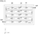
- FIG. 8 is a (second) view of a configuration of a bottom cell module 200 viewed in the Z direction.
- Cell interconnectors 235 in this example are conductors that connect the m bottom cells 210 in series by connecting a front surface (the front side in FIG. 8 ) and a back surface (the back side in FIG. 8 ) of adjacent bottom cells 210.
- FIG. 9 is a (second) view of the configuration of the bottom cell module 200 viewed in the Y direction.
- each bottom cell 210 includes, for example, n-electrodes 221, an antireflection film 220, an n-type semiconductor 222, a p-type semiconductor 223, and a p-electrode 224 that are laminated in order from the top cell module 100 side.
- the bottom cell 210 generates a voltage between the p-type semiconductor 223p and the n-type semiconductor 222.
- the generated voltage becomes a voltage between the p-electrode 224 and the n-electrodes 221. This voltage is boosted and extracted by connecting the bottom cells 210 in series through the cell interconnectors 235.
- the bottom cell module 200 include monocrystalline, polycrystalline, heterojunction, and amorphous silicon-based solar cells, and CIS-based and CIGS-based compound solar cells and the cell electrode (p-electrode, n-electrode) structure may be combined with a metal wrap through structure or a double-sided light-receiving structure.
- the metal wrap through structure is an electrode structure in which n-electrodes 221 extend through the bottom cell 210 in the thickness direction and reach the back surface thereof in the structure shown in FIG. 9 .
- the double-sided light-receiving structure is an electrode structure in which p-electrodes 224 are wired through a bus bar like the n-electrodes 221, rather than being arranged over the entire back surface of the bottom cell 210, in the structure shown in FIG. 9 .
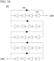
- FIG. 10 is an equivalent circuit diagram of the bottom cell module 200. As shown, the bottom cell module 200 has a circuit configuration in which bottom cells are connected in a one-in-parallel, 20-in-series configuration.
- the top cell module 100 has a larger number of parallel connections than the bottom cell module 200 and the output current of the top cell module 100 is larger than the output current of one top cell 110.
- the output current of the top cell module 100 is 1/ ⁇ of the output current of the bottom cell module 200 due to the current ratio described above and the currents of the top cell module 100 and the bottom cell module 200 do not match and therefore it is difficult to connect the top cell modules 100 and the bottom cell module 200 in series.
- the solar cell 1 of the embodiment increases the number of parallel connections of the top cell modules 100, such that it is possible to eliminate the difference between the output current of the top cell module 100 and the output current of the bottom cell module 200, approaching a current-matched state.
- the top cell module 100 and the bottom cell module 200 can be connected in series and power generated by the top cell module 100 and the bottom cell module 200 can be efficiently used.
- the weight of the solar cell 1 can also be reduced since the number of positive terminals 1P and the number of negative terminals 1N of the solar cell 1 can each be reduced to one.
- connection mode of the plurality of top cells 110 and the connection mode of the plurality of bottom cells 210 are set to match the current ratio ⁇ between the top cells 110 and the bottom cells 210 and thus power generated by the top cell module and the bottom cell module can be efficiently used.
- FIG. 11 is a configuration diagram of a solar cell system according to the first embodiment.
- Each solar cell 1 is geometrically configured such that the positive terminal 100P of the top cell module 100 (that is, the positive terminal 1P of the solar cell 1) and the negative terminal 200N of the bottom cell module 200 (that is, the negative terminal 1N of the solar cell 1) are arranged at one corner of the solar cell 1.
- FIG. 11 if an upper solar cell 1 is rotated 180 degrees about the Z-axis, it will match a lower solar cell 1 and thus both are equivalent.
- the solar cells 1 are arranged adjacent to each other and the positive terminal 1P and the negative terminal 1N of solar cells 1 adjacent to each other in the X direction are connected.
- Such a configuration produces a solar cell system in which a plurality of solar cells 1 are connected in series. Power generated by the solar cell system is input to an input terminal 310 of a power conditioning system (PCS) 300 and output through an output terminal 320.
- PCS power conditioning system
- FIG. 12 is a configuration diagram of a solar cell 2 of the second embodiment.
- the solar cell 2 differs from the solar cell 1 of the first embodiment in that a negative terminal 100N of a top cell module 100 is not connected to a positive terminal 200P of a bottom cell module 200, a positive terminal 100P of the top cell module 100 doubles as a first positive terminal 2P#1 of the solar cell 2, the negative terminal 100N of the top cell module 100 doubles as a first negative terminal 2N#1 of the solar cell 2, the positive terminal 200P of the bottom cell module 200 doubles as a second positive terminal 2P#1 of the solar cell 2, and a negative terminal 200N of the bottom cell module 200 doubles as a second negative terminal 2N#1 of the solar cell 2.
- the top cell module 100 and the bottom cell module 200 function as independent solar cells.
- the internal configurations of the top cell module 100 and the bottom cell module 200 are the same as those of the first embodiment and description thereof will be omitted.
- FIG. 13 is a configuration diagram of a solar cell system according to the second embodiment.
- Each solar cell 2 can be formed as one of two types of geometric configurations, type A and type B.
- the solar cell 2 (of type A) is that in which the positive terminal 100P of the top cell module 100 (that is, the first positive terminal 2P#1 of the solar cell 2) is present at a first corner when viewed from the light incident side (from the positive Z side).
- the first corner is the upper right corner or the lower left corner, and if the solar cell 2 is rotated 180 degrees about the Z-axis, there is no distinction between the upper right corner and the lower left corner and thus these corners are equivalent.
- the solar cell 2 (of type B) is that in which the positive terminal 100P of the top cell module 100 (that is, the first positive terminal 2P#1 of the solar cell 2) is present at a second corner when viewed from the light incident side (from the positive Z side).
- the second corner is a corner adjacent to the first corner, which is either lower right or upper left. If the solar cell 2 has a square shape, there is no difference between the types A and B, but this is not the case.
- the solar cell 2 (of type A) is an example of a "solar cell of a first type”
- the solar cell 2 (of type B) is an example of a "solar cell of a second type.”
- the solar cells 2 (of type A) and the solar cells 2 (of type B) are alternately arranged in the arrangement direction (the X direction), and at the connection point between a solar cell 2 (of type A) and a solar cell 2 (of type B) that are adjacent to each other, the first positive terminal 2P#1 of the solar cell 2 (of type A) and 2N#1 of the solar cell 2 (of type B) are connected and 2P#2 of the solar cell 2 (of type A) and 2N#2 of the solar cell 2 (of type B) are connected (see (1) in FIG.
- Such a configuration produces a front cell solar cell system in which top cell modules 100 of a plurality of solar cells 2 are connected in series and a bottom cell solar cell system in which bottom cell modules 200 of a plurality of solar cells 2 are connected in series.
- Power generated by the front cell solar cell system and power generated by the bottom cell solar cell system are input respectively to a first input terminal 310#1 and a second input terminal 310#2 of a power conditioning system (PCS) 300, processing such as current matching is performed in the PCS 300, and integrated power is output through an output terminal 320.
- PCS power conditioning system
- the bottom cell module 200 includes a number of bottom cells 210 equal to the number of top cells 110.
- the plurality of top cells 110 includes a plurality of top cells 110 arranged in a first direction (the X direction) and the plurality of top cells 110 and the plurality of bottom cells 210 are arranged to face each other in a one-to-one correspondence in plan view.
- a set of top cells 110 arranged in the X direction such as the top cells 110-1 to 110-4 corresponds to the "plurality of top cells 110 arranged in the first direction (the X direction)."
- an electrode connecting the plurality of top cells 110 is positioned such that the electrode does not overlap the bottom cells 210 in plan view. Accordingly, it is possible to limit a decrease in the amount of power generated by the bottom cells. This will be explained below.
- Each of the plurality of top cells 110 has a portion that protrudes relative to a bottom cell 210 facing the top cell (for example, a bottom cell 210 having the same reference numeral after the hyphen) among the plurality of bottom cells 210 in a second direction (the Y direction) orthogonal to the first direction (the X direction) in plan view, and the protruding portion is provided with a first electrode that connects the plurality of top cells 110 arranged in the first direction in parallel.
- the first electrode includes a positive-side cell interconnector 120P and a negative-side cell interconnector 120N.
- a second electrode (a string connector 130) connecting the first electrodes protrudes outside of the plurality of top cells 110 in the first direction (the X direction) in plan view. That is, the first electrodes extend, in the X direction, to the outside of the ends (outer edge lines) of top cells 110 positioned at both ends among the top cells 110 arranged in the X direction and a second electrode connects ends of the first electrodes.
- the first electrodes extend, in the X direction, to the outside of the ends (outer edge lines) of top cells 110 positioned at both ends among the top cells 110 arranged in the X direction and a second electrode connects ends of the first electrodes.
- a positive-side cell interconnector 120P extends beyond an X-direction end of a top cell 110-4
- a negative-side cell interconnector 120N extends beyond an X-direction end of a top cell 110-8
- a string connector 130 connects tips of the cell interconnectors.
- an electrode including at least a first electrode and may include a second electrode
- connecting the plurality of top cells 110 is positioned such that the electrode does not overlap the bottom cells 210 in plan view.
- FIG. 14 is a plan view of the solar cell 1 or 2.
- FIG. 15 is a cross-sectional view along line 15-15 of FIG. 14 .
- the configuration illustrated in FIG. 7 and the configuration illustrated in FIG. 9 are not distinguished and the cell interconnectors 230 and the cell interconnectors 235 are omitted.
- the dimensions and scale are not as shown in FIGS. 14 and 15 and may be changed arbitrarily.
- a supplementary description will be given of the material or the like of each component.
- the n-compound layer 112 is a semiconductor that forms a pn junction with a light absorbing layer, and in the case of cuprous oxide, an oxide semiconductor is used as the n-compound layer 112.
- the n-compound layer 112 preferably has a high transmittance.
- the p-light absorbing layer 113 is a light absorbing layer of the solar cell and preferably has a high transmittance in order to allow the bottom cell 210 to transmit light of wavelengths other than those absorbed by the light absorbing layer.
- cuprous oxide Cu 2 O is used as the p-light absorbing layer 113.
- the hatching of the substrate 115 corresponds to a "resin,” the substrate 115 may be glass as described above.
- Each of the cell interconnectors 120N and 120P is, for example, a solder-plated copper wire, a conductive tape, a combination of a conductive adhesive and a copper foil, or a copper foil with a resin or the like adhered to one side thereof.
- the conductive tape is, for example, a combination of a copper foil plated with Sn or the like and a resin-based adhesive.
- the top cell 110 is provided with protruding portions 110hP and 110hN that protrude outside of the ends of the bottom cell 210 in the Y direction, the positive-side cell interconnector 120P is arranged to be received in the protruding portion 110hP, and the negative-side cell interconnector 120N is arranged to be received in the protruding portion 110hN.
- the width of each of the protruding portions 110hP and 110hN is, for example, approximately 0 to 10 mm, more preferably approximately 0 to 3 mm.
- the positive-side cell interconnector 120P is arranged in contact with the p-electrode 114, but in FIG. 15 , the positive-side cell interconnector 120P is arranged in contact with an isolated n-electrode 111 (which is to be semantically called a p-electrode) which is provided on the p-electrode 114 and arranged apart from the main laminated structure in the Y direction.
- an isolated n-electrode 111 which is to be semantically called a p-electrode
- a current flows passes through the n-electrode 111, the n-compound layer 112, the p-light absorbing layer 113, and the p-electrode 114, starting from the negative-side cell interconnector 120N, and further passes through the isolated n-electrode 111 and reaches the positive-side cell interconnector 120P.
- the portion between the protruding portions 110hP and 110hN may have a structure that is scribed in the X direction at a plurality of locations.
- an electrode connecting the plurality of top cells 110 is positioned such that the electrode does not overlap the bottom cells 210 in plan view.
- a top cell module 100 configured to generate power by photoelectrically converting incident light and allow part of the incident light to pass through the top cell module 100 and a bottom cell module 200 laminated to the top cell module 100, the bottom cell module 200 being configured to generate power by photoelectrically converting light that has passed through the top cell module 100, wherein the top cell module 100 includes a plurality of top cells 110 that are connected in series, in parallel, or in a combination of series and parallel, the bottom cell module 200 includes a plurality of bottom cells 210 that are connected in series, in parallel, or in a combination of series and parallel, the number of the bottom cells 210 being equal to the number of the top cells 110, and an electrode connecting the plurality of top cells 110 is positioned such that the electrode does not overlap the bottom cells 210 in plan view. Accordingly, it is possible to limit a decrease in the amount of power generated by the bottom cells 210 due to the shadow of the electrode on the bottom cells 210.
- the solar cell or the solar cell system of each embodiment can efficiently generate power in a small space, such that it can be suitably mounted at various locations with many restrictions such as the wing surfaces of aircrafts.
Landscapes
- Photovoltaic Devices (AREA)
- Life Sciences & Earth Sciences (AREA)
- Engineering & Computer Science (AREA)
- Sustainable Development (AREA)
- Sustainable Energy (AREA)
Abstract
Description
- Embodiments of the present invention relate to a solar cell and a solar cell system.
- A tandem solar cell including a top cell module and a bottom cell module is known in the related art. A tandem solar cell can efficiently generate power in a small area by combining a top cell module and a bottom cell module formed of materials having different light absorption bands.
-
- [Patent Document 1]
Japanese Unexamined Patent Application, First Publication No. 2020-53669 - [Patent Document 2]
Published Japanese Translation No.2017-534184 - In the tandem solar cell, it is assumed that the top cell module includes a plurality of top cells and the bottom cell module includes a plurality of bottom cells. However, in the technology of the related art, electrodes connecting a plurality of top cells may overlap bottom cells in plan view, resulting in a decrease in the amount of power generated by the bottom cells.
- It is an object of the present invention to provide a solar cell and a solar cell system capable of limiting a decrease in the amount of power generated by bottom cells.
- A solar cell of an embodiment includes a top cell module and a bottom cell module. The top cell module generates power by photoelectrically converting incident light and allows part of the incident light to pass through the top cell module. The bottom cell module is laminated to the top cell module and generates power by photoelectrically converting light that has passed through the top cell module. The top cell module includes a plurality of top cells that are connected in series, in parallel, or in a combination of series and parallel. The bottom cell module includes a plurality of bottom cells that are connected in series, in parallel, or in a combination of series and parallel, the number of the bottom cells being equal to the number of the top cells. An electrode connecting the plurality of top cells is positioned such that the electrode does not overlap the bottom cells in plan view.
-
-
FIG. 1 is a configuration diagram of asolar cell 1 according to a first embodiment. -
FIG. 2 is a view of a configuration of atop cell module 100 viewed in a Z direction. -
FIG. 3 is a perspective view showing an example of a laminated structure of eachtop cell 110. -
FIG. 4 is a side view showing an example of the laminated structure of thetop cell 110. -
FIG. 5 is an equivalent circuit diagram of thetop cell module 100. -
FIG. 6 is a (first) view of a configuration of abottom cell module 200 viewed in the Z direction. -
FIG. 7 is a (first) view of the configuration of thebottom cell module 200 viewed in a Y direction. -
FIG. 8 is a (second) view of a configuration of abottom cell module 200 viewed in the Z direction. -
FIG. 9 is a (second) view of the configuration of thebottom cell module 200 viewed in the Y direction. -
FIG. 10 is an equivalent circuit diagram of thebottom cell module 200. -
FIG. 11 is a configuration diagram of a solar cell system according to the first embodiment. -
FIG. 12 is a configuration diagram of asolar cell 2 of a second embodiment. -
FIG. 13 is a configuration diagram of a solar cell system according to the second embodiment. -
FIG. 14 is a plan view of thesolar cell -
FIG. 15 is a cross-sectional view along line 15-15 ofFIG. 14 . - A solar cell and a solar cell system according to embodiments will be described below with reference to the drawings.
-
FIG. 1 is a configuration diagram of asolar cell 1 according to a first embodiment. Thesolar cell 1 includes atop cell module 100 and abottom cell module 200. Each of thetop cell module 100 and thebottom cell module 200 has, for example, a flat plate shape having a rectangular surface and thetop cell module 100 and thebottom cell module 200 are stacked in the thickness direction. Hereinafter, the extending direction of one side of the rectangular surface of each of thetop cell module 100 and thebottom cell module 200 is defined as an X direction, the extending direction of another side thereof is defined as a Y direction, and the thickness direction is defined as a Z direction. An arrow D inFIG. 1 indicates the direction of incidence of light (sunlight). The same applies toFIGS. 3 ,4 ,7 ,9 and11 which will be described later. Thesolar cell 1 is installed such that light is incident on the rectangular surface of thetop cell module 100 on the side opposite to thebottom cell module 200. - The
top cell module 100 generates power by photoelectrically converting incident light while allowing part of the incident light to pass through thetop cell module 100. Thebottom cell module 200 generates power by photoelectrically converting light that has passed through thetop cell module 100. Apositive terminal 100P of thetop cell module 100 doubles as apositive terminal 1P of thesolar cell 1. Anegative terminal 100N of thetop cell module 100 is connected to apositive terminal 200P of thebottom cell module 200. Anegative terminal 200N of thebottom cell module 200 doubles as anegative terminal 1N of thesolar cell 1. Thus, in the first embodiment, thetop cell module 100 and thebottom cell module 200 are connected in series between thepositive terminal 1P and thenegative terminal 1N of thesolar cell 1. - The
top cell module 100 includes a plurality of top cells 110 (shown later) that are connected in series, in parallel, or in a combination of series and parallel and thebottom cell module 200 includes a plurality of bottom cells 210 (shown later) that are connected in series, in parallel, or in a combination of series and parallel. As will be described later, the connection mode of the plurality oftop cells 110 and the connection mode of the plurality ofbottom cells 210 may be set to match the current ratio between atop cell 110 and abottom cell 210. The current ratio is the ratio between power generated by atop cell 110 and power generated by abottom cell 210 when light of an assumed component is incident. Hereinafter, the current ratio (top cell output current:bottom cell output current) is expressed as 1:α. α>1 since thebottom cell 210 normally outputs more current. -
FIG. 2 is a view of a configuration of thetop cell module 100 viewed in the Z direction. Thetop cell module 100 includes, for example, a plurality of top cells 110-1 to m, positive-side cell interconnectors 120P, negative-side cell interconnectors 120N,string connectors 130, anddiodes 140. m is an arbitrary natural number equal to or greater than 2 and m = 20 inFIG. 2 . Each top cell will be simply referred to as atop cell 110 when there is no distinction as to which top cell it is. Each negative-side cell interconnector 120N is a conductor that commonly connects n-electrodes 111 (shown later) oftop cells 110 arranged in the X direction. Each positive-side cell interconnector 120P is a conductor that commonly connects p-electrodes 114 (shown later) of thetop cells 110 arranged in the X direction. Thus, in the configuration ofFIG. 2 , fourtop cells 110 are connected in parallel. Eachdiode 140 is a bypass diode provided for every fourtop cells 110 connected in parallel. Eachdiode 140 bypasses a current flowing through corresponding fourtop cells 110 when the corresponding fourtop cells 110 are shaded or fail. Thetop cell module 100 is joined to thebottom cell module 200 via a resin containing a sealing material, an adhesive film, or the like. -
FIG. 3 is a perspective view showing an example of a laminated structure of eachtop cell 110.FIG. 4 is a side view showing an example of the laminated structure of thetop cell 110. Thetop cell 110 is, for example, a cuprous oxide solar cell and has, for example, a configuration in which an n-electrode 111, an n-compound layer 112, a p-lightabsorbing layer 113, a p-electrode 114, and asubstrate 115 are laminated in order from the negative-side cell interconnector 120N side. The configuration shown inFIGS. 3 and4 is merely an example and any configuration can be adopted as long as it is a configuration capable of generating power by photoelectrically converting incident light while allowing part of the incident light to pass therethrough. For example, a cuprous oxide (Cu2O) solar cell, a dye-sensitized solar cell, an organic thin film solar cell, or a perovskite solar cell is adopted as thetop cell 110. A protective film, a sealing material, and the like may be appropriately added to the configuration shown inFIGS. 3 and4 . An antireflection film may be formed on the n-compound layer 112 for the purpose of facilitating introduction of light into the power generation layer. The n-electrode 111 and the p-electrode 114 are, for example, transparent conductive films or electrodes formed in a mesh shape and allow light to pass through gaps of the mesh. Thesubstrate 115 is, for example, a transparent film of such as glass or PET, and the higher the light transmittance, the better. Thetop cell 110 generates a voltage between the n-compound layer 112 and the p-lightabsorbing layer 113. The generated voltage becomes a voltage between the n-electrode 111 and the p-electrode 114 and this voltage is extracted by the negative-side cell interconnector 120N and the positive-side cell interconnector 120P.FIG. 5 is an equivalent circuit diagram of thetop cell module 100. As shown, thetop cell module 100 has a circuit configuration in whichtop cells 110 are connected in a four-in-parallel, five-in-series configuration. - Each
bottom cell 210 is, for example, a back-contact solar cell. An exemplary configuration in this case is shown inFIGS. 6 and7 .FIG. 6 is a (first) view of a configuration of thebottom cell module 200 viewed in the Z direction. Thebottom cell module 200 includes, for example, a plurality of bottom cells 210-1 to m,cell interconnectors 230, anddiodes 240. Each bottom cell will be simply referred to as abottom cell 210 when there is no distinction as to which bottom cell it is. The cell interconnectors 230 are conductors that are provided between adjacentbottom cells 210 and connect them bottom cells 210 in series. Eachdiode 240 is a bypass diode provided for every fourbottom cells 210 connected in series. Eachdiode 240 bypasses a current flowing through corresponding fourbottom cells 210 when the corresponding fourbottom cells 210 are shaded or fail. -
FIG. 7 is a (first) view of the configuration of thebottom cell module 200 viewed in the Y direction. As shown, eachbottom cell 210 includes, for example, anantireflection film 211, an n-type semiconductor 212, and ap+ diffusion layer 213 or ann+ diffusion layer 214 that are laminated in order from thetop cell module 100 side. The p+ diffusion layers 213 and the n+ diffusion layers 214 are alternately arranged in the Y direction of thebottom cells 210. A protective film, a sealing material, and the like may be appropriately added to the configuration shown inFIG. 7 . Thebottom cell 210 generates a voltage between thep+ diffusion layer 213 and then+ diffusion layer 214. The generated voltage becomes voltages between p-electrodes 215 and n-electrodes 216. The p-electrodes 215 and the n-electrodes 216 are also alternately arranged in the Y direction. A plurality of p-electrodes 215 in eachbottom cell 210 are grouped together and a plurality of n-electrodes 216 in eachbottom cell 210 are also grouped together. Both voltages of eachbottom cell 210 are connected to electrodes of the opposite n or p type of its adjacentbottom cells 210 through thecell interconnectors 230, such that thebottom cells 210 are connected in series. - The
bottom cell 210 may be a solar cell of other modes such as a crystalline Si solar cell. An exemplary configuration in this case is shown inFIGS. 8 and9 .FIG. 8 is a (second) view of a configuration of abottom cell module 200 viewed in the Z direction.Cell interconnectors 235 in this example are conductors that connect them bottom cells 210 in series by connecting a front surface (the front side inFIG. 8 ) and a back surface (the back side inFIG. 8 ) of adjacentbottom cells 210. -
FIG. 9 is a (second) view of the configuration of thebottom cell module 200 viewed in the Y direction. As shown, eachbottom cell 210 includes, for example, n-electrodes 221, anantireflection film 220, an n-type semiconductor 222, a p-type semiconductor 223, and a p-electrode 224 that are laminated in order from thetop cell module 100 side. Thebottom cell 210 generates a voltage between the p-type semiconductor 223p and the n-type semiconductor 222. The generated voltage becomes a voltage between the p-electrode 224 and the n-electrodes 221. This voltage is boosted and extracted by connecting thebottom cells 210 in series through thecell interconnectors 235. Other examples of thebottom cell module 200 include monocrystalline, polycrystalline, heterojunction, and amorphous silicon-based solar cells, and CIS-based and CIGS-based compound solar cells and the cell electrode (p-electrode, n-electrode) structure may be combined with a metal wrap through structure or a double-sided light-receiving structure. The metal wrap through structure is an electrode structure in which n-electrodes 221 extend through thebottom cell 210 in the thickness direction and reach the back surface thereof in the structure shown inFIG. 9 . The double-sided light-receiving structure is an electrode structure in which p-electrodes 224 are wired through a bus bar like the n-electrodes 221, rather than being arranged over the entire back surface of thebottom cell 210, in the structure shown inFIG. 9 . -
FIG. 10 is an equivalent circuit diagram of thebottom cell module 200. As shown, thebottom cell module 200 has a circuit configuration in which bottom cells are connected in a one-in-parallel, 20-in-series configuration. - In the
solar cell 1 configured in this manner, thetop cell module 100 has a larger number of parallel connections than thebottom cell module 200 and the output current of thetop cell module 100 is larger than the output current of onetop cell 110. Here, if the number of parallel connections of thetop cell modules 100 and the number of parallel connections of thebottom cell module 200 are the same, the output current of thetop cell module 100 is 1/α of the output current of thebottom cell module 200 due to the current ratio described above and the currents of thetop cell module 100 and thebottom cell module 200 do not match and therefore it is difficult to connect thetop cell modules 100 and thebottom cell module 200 in series. In view of this, thesolar cell 1 of the embodiment increases the number of parallel connections of thetop cell modules 100, such that it is possible to eliminate the difference between the output current of thetop cell module 100 and the output current of thebottom cell module 200, approaching a current-matched state. As a result, thetop cell module 100 and thebottom cell module 200 can be connected in series and power generated by thetop cell module 100 and thebottom cell module 200 can be efficiently used. The weight of thesolar cell 1 can also be reduced since the number ofpositive terminals 1P and the number ofnegative terminals 1N of thesolar cell 1 can each be reduced to one. - Although it is desirable that a quotient β obtained by dividing the number of parallel connections of the
top cell modules 100 by the number of parallel connections of thebottom cell modules 200 match the characteristic value α, β may be slightly different from α as long as β is closer to α than to 1 (that is, the numbers of parallel connections serve to achieve current matching) and does not exceed an upper limit (for example, about 1.5×α). Since β=4 in the embodiment illustrated above, the materials of thetop cells 110 and thebottom cells 210 may be selected such that α=4. - According to the first embodiment described above, the connection mode of the plurality of
top cells 110 and the connection mode of the plurality of bottom cells 210 (that is, the quotient β) are set to match the current ratio α between thetop cells 110 and thebottom cells 210 and thus power generated by the top cell module and the bottom cell module can be efficiently used. - The
solar cells 1 having such a configuration are used, for example, in the following manner.FIG. 11 is a configuration diagram of a solar cell system according to the first embodiment. Eachsolar cell 1 is geometrically configured such that the positive terminal 100P of the top cell module 100 (that is, the positive terminal 1P of the solar cell 1) and thenegative terminal 200N of the bottom cell module 200 (that is, thenegative terminal 1N of the solar cell 1) are arranged at one corner of thesolar cell 1. InFIG. 11 , if an uppersolar cell 1 is rotated 180 degrees about the Z-axis, it will match a lowersolar cell 1 and thus both are equivalent. - As shown in
FIG. 11 , thesolar cells 1 are arranged adjacent to each other and thepositive terminal 1P and thenegative terminal 1N ofsolar cells 1 adjacent to each other in the X direction are connected. - Such a configuration produces a solar cell system in which a plurality of
solar cells 1 are connected in series. Power generated by the solar cell system is input to aninput terminal 310 of a power conditioning system (PCS) 300 and output through anoutput terminal 320. - According to the first embodiment described above, it is possible to efficiently arrange a plurality of
solar cells 1 in series with a reduced wiring length, compared to the solar cell system of the related art in which four-terminal modules are connected. - A second embodiment will be described below.
FIG. 12 is a configuration diagram of asolar cell 2 of the second embodiment. Thesolar cell 2 differs from thesolar cell 1 of the first embodiment in that anegative terminal 100N of atop cell module 100 is not connected to a positive terminal 200P of abottom cell module 200, a positive terminal 100P of thetop cell module 100 doubles as a firstpositive 1 of theterminal 2P#solar cell 2, thenegative terminal 100N of thetop cell module 100 doubles as a firstnegative 1 of theterminal 2N#solar cell 2, the positive terminal 200P of thebottom cell module 200 doubles as a secondpositive 1 of theterminal 2P#solar cell 2, and anegative terminal 200N of thebottom cell module 200 doubles as a secondnegative 1 of theterminal 2N#solar cell 2. That is, in thesolar cell 2 of the second embodiment, thetop cell module 100 and thebottom cell module 200 function as independent solar cells. The internal configurations of thetop cell module 100 and thebottom cell module 200 are the same as those of the first embodiment and description thereof will be omitted. - The
solar cells 2 having such a configuration are used, for example, in the following manner.FIG. 13 is a configuration diagram of a solar cell system according to the second embodiment. Eachsolar cell 2 can be formed as one of two types of geometric configurations, type A and type B. The solar cell 2 (of type A) is that in which the positive terminal 100P of the top cell module 100 (that is, the firstpositive 1 of the solar cell 2) is present at a first corner when viewed from the light incident side (from the positive Z side). The first corner is the upper right corner or the lower left corner, and if theterminal 2P#solar cell 2 is rotated 180 degrees about the Z-axis, there is no distinction between the upper right corner and the lower left corner and thus these corners are equivalent. The solar cell 2 (of type B) is that in which the positive terminal 100P of the top cell module 100 (that is, the firstpositive 1 of the solar cell 2) is present at a second corner when viewed from the light incident side (from the positive Z side). The second corner is a corner adjacent to the first corner, which is either lower right or upper left. If theterminal 2P#solar cell 2 has a square shape, there is no difference between the types A and B, but this is not the case. The solar cell 2 (of type A) is an example of a "solar cell of a first type," and the solar cell 2 (of type B) is an example of a "solar cell of a second type." - As shown in
FIG. 13 , the solar cells 2 (of type A) and the solar cells 2 (of type B) are alternately arranged in the arrangement direction (the X direction), and at the connection point between a solar cell 2 (of type A) and a solar cell 2 (of type B) that are adjacent to each other, the firstpositive 1 of the solar cell 2 (of type A) andterminal 2P#2N# 1 of the solar cell 2 (of type B) are connected and2P# 2 of the solar cell 2 (of type A) and2N# 2 of the solar cell 2 (of type B) are connected (see (1) inFIG. 13 ) or alternatively2N# 1 of the solar cell 2 (of type A) and2P# 1 of the solar cell 2 (of type B) are connected and2N# 2 of the solar cell 2 (of type A) and the secondpositive 2 of the solar cell 2 (of type B) are connected (see (2) interminal 2P#FIG. 13 ) - Such a configuration produces a front cell solar cell system in which
top cell modules 100 of a plurality ofsolar cells 2 are connected in series and a bottom cell solar cell system in whichbottom cell modules 200 of a plurality ofsolar cells 2 are connected in series. Power generated by the front cell solar cell system and power generated by the bottom cell solar cell system are input respectively to afirst input terminal 310#1 and asecond input terminal 310#2 of a power conditioning system (PCS) 300, processing such as current matching is performed in thePCS 300, and integrated power is output through anoutput terminal 320. - According to the second embodiment described above, in addition to achieving the same advantages as those of the first embodiment, by using solar cells of two types as illustrated in
FIG. 13 , it is possible to efficiently arrange a plurality ofsolar cells 2 in series with a reduced wiring length, compared to the case of using only cells of one type. - While the arrangements of
cell interconnectors bottom cells 210 that are adjacent in the Y direction are schematically shown in the configurations ofFIGS. 6 and8 , they may also actually be arranged to protrude outside ofbottom cells 210 in the X direction. - The arrangement of electrodes of the solar cell of the embodiment will be described in more detail below. As previously described, the
bottom cell module 200 includes a number ofbottom cells 210 equal to the number oftop cells 110. The plurality oftop cells 110 includes a plurality oftop cells 110 arranged in a first direction (the X direction) and the plurality oftop cells 110 and the plurality ofbottom cells 210 are arranged to face each other in a one-to-one correspondence in plan view. In the example ofFIG. 2 , a set oftop cells 110 arranged in the X direction such as the top cells 110-1 to 110-4 corresponds to the "plurality oftop cells 110 arranged in the first direction (the X direction)." - Here, an electrode connecting the plurality of
top cells 110 is positioned such that the electrode does not overlap thebottom cells 210 in plan view. Accordingly, it is possible to limit a decrease in the amount of power generated by the bottom cells. This will be explained below. - Each of the plurality of
top cells 110 has a portion that protrudes relative to abottom cell 210 facing the top cell (for example, abottom cell 210 having the same reference numeral after the hyphen) among the plurality ofbottom cells 210 in a second direction (the Y direction) orthogonal to the first direction (the X direction) in plan view, and the protruding portion is provided with a first electrode that connects the plurality oftop cells 110 arranged in the first direction in parallel. "In plan view" indicates, for example, "when viewed in the Z direction." "In plan view" can be rephrased as "when viewed in the direction D of incidence of assumed light" and can also be rephrased as "when viewed in a direction perpendicular to a widest planar portion of thesolar cell top cell 110 are present outside ends (outer edge lines) of thebottom cell 210 on both sides thereof in the Y direction. The first electrode includes a positive-side cell interconnector 120P and a negative-side cell interconnector 120N. - A second electrode (a string connector 130) connecting the first electrodes protrudes outside of the plurality of
top cells 110 in the first direction (the X direction) in plan view. That is, the first electrodes extend, in the X direction, to the outside of the ends (outer edge lines) oftop cells 110 positioned at both ends among thetop cells 110 arranged in the X direction and a second electrode connects ends of the first electrodes. For example, in the example ofFIG. 14 which will be described later, a positive-side cell interconnector 120P extends beyond an X-direction end of a top cell 110-4, a negative-side cell interconnector 120N extends beyond an X-direction end of a top cell 110-8, and astring connector 130 connects tips of the cell interconnectors. The same applies to other locations. With such a configuration, an electrode (including at least a first electrode and may include a second electrode) connecting the plurality oftop cells 110 is positioned such that the electrode does not overlap thebottom cells 210 in plan view. -
FIG. 14 is a plan view of thesolar cell FIG. 15 is a cross-sectional view along line 15-15 ofFIG. 14 . InFIGS. 14 and15 , the configuration illustrated inFIG. 7 and the configuration illustrated inFIG. 9 are not distinguished and thecell interconnectors 230 and thecell interconnectors 235 are omitted. The dimensions and scale are not as shown inFIGS. 14 and15 and may be changed arbitrarily. Here, a supplementary description will be given of the material or the like of each component. The n-compound layer 112 is a semiconductor that forms a pn junction with a light absorbing layer, and in the case of cuprous oxide, an oxide semiconductor is used as the n-compound layer 112. The n-compound layer 112 preferably has a high transmittance. The p-lightabsorbing layer 113 is a light absorbing layer of the solar cell and preferably has a high transmittance in order to allow thebottom cell 210 to transmit light of wavelengths other than those absorbed by the light absorbing layer. For example, cuprous oxide Cu2O is used as the p-lightabsorbing layer 113. Although the hatching of thesubstrate 115 corresponds to a "resin," thesubstrate 115 may be glass as described above. Each of thecell interconnectors - As shown in
FIG. 15 , thetop cell 110 is provided with protruding portions 110hP and 110hN that protrude outside of the ends of thebottom cell 210 in the Y direction, the positive-side cell interconnector 120P is arranged to be received in the protruding portion 110hP, and the negative-side cell interconnector 120N is arranged to be received in the protruding portion 110hN. The width of each of the protruding portions 110hP and 110hN is, for example, approximately 0 to 10 mm, more preferably approximately 0 to 3 mm. With such a configuration, the power generation area of thetop cell 110 and the power generation area of thebottom cell 210 substantially match. InFIG. 4 , the positive-side cell interconnector 120P is arranged in contact with the p-electrode 114, but inFIG. 15 , the positive-side cell interconnector 120P is arranged in contact with an isolated n-electrode 111 (which is to be semantically called a p-electrode) which is provided on the p-electrode 114 and arranged apart from the main laminated structure in the Y direction. In this case, a current flows passes through the n-electrode 111, the n-compound layer 112, the p-lightabsorbing layer 113, and the p-electrode 114, starting from the negative-side cell interconnector 120N, and further passes through the isolated n-electrode 111 and reaches the positive-side cell interconnector 120P. The portion between the protruding portions 110hP and 110hN may have a structure that is scribed in the X direction at a plurality of locations. - With the configuration illustrated here, an electrode connecting the plurality of
top cells 110 is positioned such that the electrode does not overlap thebottom cells 210 in plan view. - According to at least one embodiment described above, a
top cell module 100 configured to generate power by photoelectrically converting incident light and allow part of the incident light to pass through thetop cell module 100 and abottom cell module 200 laminated to thetop cell module 100, thebottom cell module 200 being configured to generate power by photoelectrically converting light that has passed through thetop cell module 100, are provided, wherein thetop cell module 100 includes a plurality oftop cells 110 that are connected in series, in parallel, or in a combination of series and parallel, thebottom cell module 200 includes a plurality ofbottom cells 210 that are connected in series, in parallel, or in a combination of series and parallel, the number of thebottom cells 210 being equal to the number of thetop cells 110, and an electrode connecting the plurality oftop cells 110 is positioned such that the electrode does not overlap thebottom cells 210 in plan view. Accordingly, it is possible to limit a decrease in the amount of power generated by thebottom cells 210 due to the shadow of the electrode on thebottom cells 210. - The solar cell or the solar cell system of each embodiment can efficiently generate power in a small space, such that it can be suitably mounted at various locations with many restrictions such as the wing surfaces of aircrafts.
- Although some embodiments of the present invention have been described, these embodiments have been presented by way of example and are not intended to limit the scope of the invention. These embodiments can be implemented in various other forms, and various omissions, substitutions, and changes can be made without departing from the spirit of the invention. These embodiments and modifications thereof are included in the scope or spirit of the invention as well as in the scope of the invention described in the claims and their equivalents.
Claims (8)
- A solar cell comprising:a top cell module configured to generate power by photoelectrically converting incident light and allow part of the incident light to pass through the top cell module; anda bottom cell module laminated to the top cell module, the bottom cell module being configured to generate power by photoelectrically converting light that has passed through the top cell module,wherein the top cell module includes a plurality of top cells that are connected in series, in parallel, or in a combination of series and parallel,the bottom cell module includes a plurality of bottom cells that are connected in series, in parallel, or in a combination of series and parallel, the number of the bottom cells being equal to the number of the top cells, andan electrode connecting the plurality of top cells is positioned such that the electrode does not overlap the bottom cells in plan view.
- The solar cell according to claim 1, wherein the plurality of top cells include a plurality of top cells arranged in a first direction,the plurality of top cells and the plurality of bottom cells are arranged to face each other in a one-to-one correspondence in plan view,each of the plurality of top cells has a portion that protrudes relative to a bottom cell facing the top cell among the plurality of bottom cells in a second direction orthogonal to the first direction in plan view, andthe protruding portion is provided with a first electrode that connects the plurality of top cells arranged in the first direction in parallel.
- The solar cell according to claim 2, wherein a second electrode connecting the first electrodes protrudes outside of the plurality of top cells in the first direction in plan view.
- The solar cell according to claim 1, wherein a connection mode of the plurality of top cells and a connection mode of the plurality of bottom cells are set to match a current ratio between the top cells and the bottom cells.
- The solar cell according to claim 4, wherein a positive terminal of the top cell module is a positive terminal of the solar cell,a negative terminal of the bottom cell module is a negative terminal of the solar cell, anda negative terminal of the top cell module is connected to a positive terminal of the bottom cell module.
- A solar cell system comprising a plurality of solar cells according to claim 5,wherein the plurality of solar cells are arranged such that the plurality of solar cells are adjacent to each other in at least one direction, andat a connection point of the plurality of solar cells adjacent to each other, the positive terminal of one of the plurality of solar cells adjacent to each other in the at least one direction and the negative terminal of another of the plurality of solar cells adjacent to each other are connected.
- The solar cell according to claim 4, wherein a positive terminal of the top cell module is a first positive terminal of the solar cell,a negative terminal of the top cell module is a first negative terminal of the solar cell,a positive terminal of the bottom cell module is a second positive terminal of the solar cell,a negative terminal of the bottom cell module is a second negative terminal of the solar cell.
- A solar cell system comprising one or more solar cells of a first type in which the positive terminal of the top cell module is present at a first corner when viewed from a light incident side and one or more solar cells of a second type in which the positive terminal of the top cell module is present at a second corner adjacent to the first corner when viewed from a light incident side, the solar cells being a plurality of solar cells according to claim 7,wherein the solar cells of the first type and the solar cells of the second type are arranged alternately in an arrangement direction, andat a connection point of a solar cell of the first type and a solar cell of the second type adjacent to each other,the first positive terminal of the solar cell of the first type and the first negative terminal of the solar cell of the second type are connected and the second positive terminal of the solar cell of the first type and the second negative terminal of the solar cell of the second type are connected, or alternativelythe first negative terminal of the solar cell of the first type and the first positive terminal of the solar cell of the second type are connected and the second negative terminal of the solar cell of the first type and the second positive terminal of the solar cell of the second type are connected.
Applications Claiming Priority (2)
| Application Number | Priority Date | Filing Date | Title |
|---|---|---|---|
| PCT/JP2020/035259 WO2022059134A1 (en) | 2020-09-17 | 2020-09-17 | Solar cell and solar cell system |
| PCT/JP2021/028595 WO2022059366A1 (en) | 2020-09-17 | 2021-08-02 | Solar cell and solar cell system |
Publications (2)
| Publication Number | Publication Date |
|---|---|
| EP4216284A1 true EP4216284A1 (en) | 2023-07-26 |
| EP4216284A4 EP4216284A4 (en) | 2024-09-04 |
Family
ID=80776563
Family Applications (1)
| Application Number | Title | Priority Date | Filing Date |
|---|---|---|---|
| EP21869053.5A Pending EP4216284A4 (en) | 2020-09-17 | 2021-08-02 | SOLAR CELL AND SOLAR CELL SYSTEM |
Country Status (4)
| Country | Link |
|---|---|
| US (1) | US20230207716A1 (en) |
| EP (1) | EP4216284A4 (en) |
| JP (1) | JP7547491B2 (en) |
| WO (2) | WO2022059134A1 (en) |
Families Citing this family (6)
| Publication number | Priority date | Publication date | Assignee | Title |
|---|---|---|---|---|
| WO2022259461A1 (en) | 2021-06-10 | 2022-12-15 | 株式会社東芝 | Tandem solar cell |
| EP4712339A1 (en) * | 2023-05-10 | 2026-03-18 | Kabushiki Kaisha Toshiba | Terminal box, solar cell unit, and solar cell unit connection body |
| FR3154232A1 (en) * | 2023-10-17 | 2025-04-18 | Institut Photovoltaique D'ile De France (Ipvf) | PHOTOVOLTAIC MODULE WITH INTEGRATED SERIES AND PARALLEL ASSEMBLY CONNECTIONS |
| WO2025155492A1 (en) * | 2024-01-19 | 2025-07-24 | First Solar, Inc. | Tandem photovoltaic devices and methods for testing and use of photovoltaic systems |
| CN118742055B (en) * | 2024-09-02 | 2025-02-07 | 浙江制能科技有限公司 | A perovskite photovoltaic module |
| CN119486471A (en) * | 2024-10-31 | 2025-02-18 | 昆山协鑫光电材料有限公司 | A solar cell module and voltage matching method and device thereof |
Family Cites Families (11)
| Publication number | Priority date | Publication date | Assignee | Title |
|---|---|---|---|---|
| JPH08226210A (en) * | 1995-02-21 | 1996-09-03 | Fuji Electric Corp Res & Dev Ltd | Photovoltaic roof material and construction method |
| US6353175B1 (en) * | 1999-09-17 | 2002-03-05 | Jx Crystals Inc. | Two-terminal cell-interconnected-circuits using mechanically-stacked photovoltaic cells for line-focus concentrator arrays |
| US8115093B2 (en) * | 2005-02-15 | 2012-02-14 | General Electric Company | Layer-to-layer interconnects for photoelectric devices and methods of fabricating the same |
| JP5032496B2 (en) * | 2006-11-17 | 2012-09-26 | 京セミ株式会社 | Stacked solar cell device |
| US20110017257A1 (en) * | 2008-08-27 | 2011-01-27 | Stion Corporation | Multi-junction solar module and method for current matching between a plurality of first photovoltaic devices and second photovoltaic devices |
| US8569613B1 (en) * | 2008-09-29 | 2013-10-29 | Stion Corporation | Multi-terminal photovoltaic module including independent cells and related system |
| NL2012557B1 (en) * | 2014-04-02 | 2016-02-15 | Stichting Energieonderzoek Centrum Nederland | Photovoltaic module. |
| EP3016148A1 (en) * | 2014-10-28 | 2016-05-04 | Sol Voltaics AB | Dual layer photovoltaic device |
| US20180233612A1 (en) * | 2015-09-28 | 2018-08-16 | Sharp Kabushiki Kaisha | Thin-film compound photovoltaic cell, method for manufacturing thin-film compound photovoltaic cell, thin-film compound photovoltaic cell array, and method for manufacturing thin-film compound photovoltaic cell array |
| CN108666373A (en) * | 2018-08-06 | 2018-10-16 | 珠海格力电器股份有限公司 | Photovoltaic modules |
| JP7273537B2 (en) | 2018-09-19 | 2023-05-15 | 株式会社東芝 | Solar cells, multi-junction solar cells, solar cell modules and photovoltaic power generation systems |
-
2020
- 2020-09-17 WO PCT/JP2020/035259 patent/WO2022059134A1/en not_active Ceased
-
2021
- 2021-08-02 WO PCT/JP2021/028595 patent/WO2022059366A1/en not_active Ceased
- 2021-08-02 JP JP2022550401A patent/JP7547491B2/en active Active
- 2021-08-02 EP EP21869053.5A patent/EP4216284A4/en active Pending
-
2023
- 2023-03-06 US US18/178,672 patent/US20230207716A1/en active Pending
Also Published As
| Publication number | Publication date |
|---|---|
| JPWO2022059366A1 (en) | 2022-03-24 |
| EP4216284A4 (en) | 2024-09-04 |
| JP7547491B2 (en) | 2024-09-09 |
| US20230207716A1 (en) | 2023-06-29 |
| WO2022059134A1 (en) | 2022-03-24 |
| WO2022059366A1 (en) | 2022-03-24 |
Similar Documents
| Publication | Publication Date | Title |
|---|---|---|
| US20230207716A1 (en) | Solar cell and solar cell system | |
| US12212146B2 (en) | Solar cell assembly | |
| KR20100026291A (en) | Thin film solar cell module and method of manufacturing the same | |
| JP7521121B2 (en) | Tandem Solar Cell | |
| US11769847B2 (en) | Solar panel with four terminal tandem solar cell arrangement | |
| US8569613B1 (en) | Multi-terminal photovoltaic module including independent cells and related system | |
| JP7266444B2 (en) | Solar cell module and solar cell system | |
| EP4589844A1 (en) | Photovoltaic module | |
| US12328953B2 (en) | Solar cell module | |
| US20260114054A1 (en) | Solar module with three-terminal tandem solar cells | |
| US12495622B2 (en) | Solar-cell module | |
| US12610628B2 (en) | Solar-cell module | |
| JP2018037481A (en) | Solar cell module and method for manufacturing solar cell module | |
| CN117997265A (en) | Intelligent junction box system for multi-junction photovoltaic module based on perovskite structure | |
| EP4589843A1 (en) | Output line connection structure for solar cell module | |
| EP4564438A1 (en) | Solar cell module | |
| WO2023248256A1 (en) | Three-dimensional photovoltaic supercell and a three-dimensional photovoltaic supercell module and method of manufacture of the same |
Legal Events
| Date | Code | Title | Description |
|---|---|---|---|
| STAA | Information on the status of an ep patent application or granted ep patent |
Free format text: STATUS: THE INTERNATIONAL PUBLICATION HAS BEEN MADE |
|
| PUAI | Public reference made under article 153(3) epc to a published international application that has entered the european phase |
Free format text: ORIGINAL CODE: 0009012 |
|
| STAA | Information on the status of an ep patent application or granted ep patent |
Free format text: STATUS: REQUEST FOR EXAMINATION WAS MADE |
|
| 17P | Request for examination filed |
Effective date: 20230303 |
|
| AK | Designated contracting states |
Kind code of ref document: A1 Designated state(s): AL AT BE BG CH CY CZ DE DK EE ES FI FR GB GR HR HU IE IS IT LI LT LU LV MC MK MT NL NO PL PT RO RS SE SI SK SM TR |
|
| DAV | Request for validation of the european patent (deleted) | ||
| DAX | Request for extension of the european patent (deleted) | ||
| REG | Reference to a national code |
Ref country code: DE Ref legal event code: R079 Free format text: PREVIOUS MAIN CLASS: H01L0031043000 Ipc: H01L0025040000 |
|
| A4 | Supplementary search report drawn up and despatched |
Effective date: 20240806 |
|
| RIC1 | Information provided on ipc code assigned before grant |
Ipc: H01L 31/042 20140101ALI20240731BHEP Ipc: H01L 31/05 20140101ALI20240731BHEP Ipc: H01L 25/04 20230101AFI20240731BHEP |