EP4212927A1 - Optical diffraction element and optical computing system - Google Patents
Optical diffraction element and optical computing system Download PDFInfo
- Publication number
- EP4212927A1 EP4212927A1 EP21852022.9A EP21852022A EP4212927A1 EP 4212927 A1 EP4212927 A1 EP 4212927A1 EP 21852022 A EP21852022 A EP 21852022A EP 4212927 A1 EP4212927 A1 EP 4212927A1
- Authority
- EP
- European Patent Office
- Prior art keywords
- light
- diffraction element
- polarized components
- light diffraction
- polarized
- Prior art date
- Legal status (The legal status is an assumption and is not a legal conclusion. Google has not performed a legal analysis and makes no representation as to the accuracy of the status listed.)
- Granted
Links
Images

Classifications
-
- G—PHYSICS
- G02—OPTICS
- G02B—OPTICAL ELEMENTS, SYSTEMS OR APPARATUS
- G02B27/00—Optical systems or apparatus not provided for by any of the groups G02B1/00 - G02B26/00, G02B30/00
- G02B27/28—Optical systems or apparatus not provided for by any of the groups G02B1/00 - G02B26/00, G02B30/00 for polarising
- G02B27/286—Optical systems or apparatus not provided for by any of the groups G02B1/00 - G02B26/00, G02B30/00 for polarising for controlling or changing the state of polarisation, e.g. transforming one polarisation state into another
-
- G—PHYSICS
- G02—OPTICS
- G02B—OPTICAL ELEMENTS, SYSTEMS OR APPARATUS
- G02B5/00—Optical elements other than lenses
- G02B5/18—Diffraction gratings
- G02B5/1814—Diffraction gratings structurally combined with one or more further optical elements, e.g. lenses, mirrors, prisms or other diffraction gratings
-
- G—PHYSICS
- G02—OPTICS
- G02B—OPTICAL ELEMENTS, SYSTEMS OR APPARATUS
- G02B27/00—Optical systems or apparatus not provided for by any of the groups G02B1/00 - G02B26/00, G02B30/00
- G02B27/28—Optical systems or apparatus not provided for by any of the groups G02B1/00 - G02B26/00, G02B30/00 for polarising
- G02B27/283—Optical systems or apparatus not provided for by any of the groups G02B1/00 - G02B26/00, G02B30/00 for polarising used for beam splitting or combining
-
- G—PHYSICS
- G02—OPTICS
- G02B—OPTICAL ELEMENTS, SYSTEMS OR APPARATUS
- G02B27/00—Optical systems or apparatus not provided for by any of the groups G02B1/00 - G02B26/00, G02B30/00
- G02B27/42—Diffraction optics, i.e. systems including a diffractive element being designed for providing a diffractive effect
- G02B27/4261—Diffraction optics, i.e. systems including a diffractive element being designed for providing a diffractive effect having a diffractive element with major polarization dependent properties
-
- G—PHYSICS
- G02—OPTICS
- G02B—OPTICAL ELEMENTS, SYSTEMS OR APPARATUS
- G02B27/00—Optical systems or apparatus not provided for by any of the groups G02B1/00 - G02B26/00, G02B30/00
- G02B27/42—Diffraction optics, i.e. systems including a diffractive element being designed for providing a diffractive effect
- G02B27/4272—Diffraction optics, i.e. systems including a diffractive element being designed for providing a diffractive effect having plural diffractive elements positioned sequentially along the optical path
- G02B27/4277—Diffraction optics, i.e. systems including a diffractive element being designed for providing a diffractive effect having plural diffractive elements positioned sequentially along the optical path being separated by an air space
-
- G—PHYSICS
- G02—OPTICS
- G02B—OPTICAL ELEMENTS, SYSTEMS OR APPARATUS
- G02B27/00—Optical systems or apparatus not provided for by any of the groups G02B1/00 - G02B26/00, G02B30/00
- G02B27/42—Diffraction optics, i.e. systems including a diffractive element being designed for providing a diffractive effect
- G02B27/44—Grating systems; Zone plate systems
-
- G—PHYSICS
- G02—OPTICS
- G02B—OPTICAL ELEMENTS, SYSTEMS OR APPARATUS
- G02B5/00—Optical elements other than lenses
- G02B5/18—Diffraction gratings
-
- G—PHYSICS
- G02—OPTICS
- G02B—OPTICAL ELEMENTS, SYSTEMS OR APPARATUS
- G02B5/00—Optical elements other than lenses
- G02B5/30—Polarising elements
-
- G—PHYSICS
- G02—OPTICS
- G02B—OPTICAL ELEMENTS, SYSTEMS OR APPARATUS
- G02B5/00—Optical elements other than lenses
- G02B5/30—Polarising elements
- G02B5/3025—Polarisers, i.e. arrangements capable of producing a definite output polarisation state from an unpolarised input state
-
- G—PHYSICS
- G02—OPTICS
- G02F—OPTICAL DEVICES OR ARRANGEMENTS FOR THE CONTROL OF LIGHT BY MODIFICATION OF THE OPTICAL PROPERTIES OF THE MEDIA OF THE ELEMENTS INVOLVED THEREIN; NON-LINEAR OPTICS; FREQUENCY-CHANGING OF LIGHT; OPTICAL LOGIC ELEMENTS; OPTICAL ANALOGUE/DIGITAL CONVERTERS
- G02F3/00—Optical logic elements; Optical bistable devices
-
- G—PHYSICS
- G02—OPTICS
- G02B—OPTICAL ELEMENTS, SYSTEMS OR APPARATUS
- G02B5/00—Optical elements other than lenses
- G02B5/32—Holograms used as optical elements
Definitions
- the present invention relates to a light diffraction element which carries out optical computing. Moreover, the present invention relates to an optical computing system which includes such a light diffraction element.
- a light diffraction element that includes a plurality of microcells each of which has an individually set refractive index. This light diffraction element is designed such that light beams which have passed through the microcells are caused to interfere with each other to optically carry out predetermined computing.
- the optical computing using the light diffraction element can be carried out at a higher speed and low power consumption, as compared with electrical computing using a processor.
- Patent Literature 1 discloses an optical neural network having an input layer, an intermediate layer, and an output layer. The above light diffraction element can be utilized as, for example, an intermediate layer for such an optical neural network.
- Patent Literature 1 Specification of US Patent No. 7847225
- An aspect of the present invention is accomplished in view of the problem, and its object is to provide a light diffraction element which can output signal light indicative of information before the computing, in addition to signal light indicative of information after the computing.
- the light diffraction element in accordance with an aspect of the present invention is a light diffraction element constituted by a plurality of cells.
- first regions of respective of the plurality of cells allow first polarized components to pass through and have respective thicknesses or refractive indices that are independently set; and second regions of respective of the plurality of cells allow second polarized components to pass through and have uniform thicknesses or uniform refractive indices, the second polarized components being different in polarization direction from the first polarized components.
- the optical computing system in accordance with an aspect of the present invention includes: the light diffraction element; a light-emitting device that outputs signal light to be input to the light diffraction element; and a light-receiving device that detects, without distinction, the first polarized components and the second polarized components of signal light which is output from the light diffraction element.
- the optical computing system in accordance with an aspect of the present invention includes: the light diffraction element; a light-emitting device that outputs signal light to be input to the light diffraction element; a first light-receiving device that detects the first polarized components of signal light output from the light diffraction element: and a second light-receiving device that detects the second polarized components of the signal light output from the light diffraction element.
- a light diffraction element which can output signal light indicative of information before the computing, in addition to signal light indicative of information after the computing.
- an optical computing system which includes such a light diffraction element.
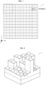
- Fig. 1 is a plan view illustrating the light diffraction element 1.
- Fig. 2 is a perspective view in which a part (surrounded by the dashed lines in Fig. 1 ) of the light diffraction element 1 is magnified.
- the light diffraction element 1 is a planar light diffraction element and is constituted by a plurality of microcells (an example of "cell” in claims).
- the term "microcell” refers to, for example, a cell having a cell size of less than 10 pm.
- the term "cell size" refers to a square root of an area of a cell. For example, when a shape of a microcell in a plan view is a square shape, the cell size is a length of one side of the cell.
- a lower limit of the cell size is not particularly limited and can be, for example, 1 nm.
- the light diffraction element 1 illustrated in Fig. 1 is constituted by 12 ⁇ 12 microcells which are arranged in a matrix manner.
- a shape of each of the microcells in a plan view is a square shape having a size of 1 pm ⁇ 1 pm
- a shape of the light diffraction element 1 in a plan view is a square shape having a size of 12 ⁇ m ⁇ 12 pm.
- Each of the microcells includes a first region C1 which selectively allows a first polarized component contained in signal light to pass through, and a second region C2 which selectively allows a second polarized component contained in the signal light to pass through.
- thicknesses or refractive indices of the respective first regions C 1 are independently set. According to the configuration, phase change amounts of the first polarized components passing through the microcells are independently set.
- the second regions C2 in the respective microcells are set to have uniform thicknesses or uniform refractive indices. According to the configuration, phase conversion amounts of the second polarized components passing through the microcells are uniformly set. Therefore, the light diffraction element 1 selectively acts on the first polarized components of signal light.
- the light diffraction element 1 causes only the first polarized components of signal light, which have passed through the microcells, to interfere with each other to carry out predetermined optical computing. Therefore, the first polarized components of an optical signal output from the light diffraction element 1 become an optical signal indicative of information after the computing, while the second polarized components of signal light output from the light diffraction element 1 become an optical signal indicative of information before the computing.
- “selectively allowing the first polarized components to pass through” and “selectively acting on the first polarized components” mean, in other words, that "a transmittance of the first polarized components is higher than a transmittance of the second polarized components".
- “selectively allowing the second polarized components to pass through” means, in other words, that "a transmittance of the second polarized components is higher than a transmittance of the first polarized components”.
- the first polarized components (on which the light diffraction element 1 acts) only need to be polarized components having the polarization direction different from that of the second polarized components (on which the light diffraction element 1 does not act).
- X polarized light which is linear polarized light whose polarization plane is parallel to a Z-X plane
- Y polarized light (which is linear polarized light whose polarization plane is parallel to a Y-Z plane) is set as the second polarized component.
- right circular polarized light is set as the first polarized component
- left circular polarized light is set as the second polarized component.
- the light diffraction element 1 a light diffraction element in the former form, i.e., the light diffraction element 1 which selectively acts on X polarized light is employed.
- the light diffraction element 1 in which the transmittance of X polarized light is higher than the transmittance of Y polarized light is employed.
- Each of the first regions C 1 and the second regions C2 in the microcells of the light diffraction element 1 which selectively acts on X polarized light can be constituted by, for example, a pillar that has an emission surface on which a polarizing filter is provided (see Fig. 2 ).
- the polarizing filter that is provided on the emission surface of the pillar constituting the first region C1 is a polarizing filter which selectively allows X polarized light to pass through (i.e., the transmittance of X polarized light is higher than the transmittance of Y polarized light).
- the polarizing filter that is provided on the emission surface of the pillar constituting the second region C2 is a polarizing filter which selectively allows Y polarized light to pass through (i.e., the transmittance of Y polarized light is higher than the transmittance of X polarized light).
- This makes it possible to set the phase change amount with respect to X polarized light of each microcell in accordance with the height of the pillar, while setting the phase change amounts with respect to Y polarized light of the microcells to be uniform. That is, it is possible to provide the light diffraction element 1 which selectively acts on X polarized light.
- the polarizing filter it is possible to use, for example, a metasurface.
- the polarizing filter can be provided on an incidence surface of each pillar instead of being provided on the emission surface of each pillar, or can be provided on both the incidence surface and the emission surface of each pillar.
- the thickness or refractive index of the first region C1 of each of the microcells can be set, for example, by using machine learning.
- a model that is used in the machine learning can be, for example, a model to which an intensity distribution of signal light input to the light diffraction element 1 is input, and from which an intensity distribution of the first polarized components of signal light output from the light diffraction element 1 is output.
- the model contains thicknesses or refractive indices of the first regions C1 of the microcells as parameters.
- Fig. 3 is a perspective view illustrating a main part configuration of an optical computing system 10A for carrying out such optical computing.
- the optical computing system 10A includes a light-emitting device 2 and a light-receiving device 3, in addition to the light diffraction element 1.
- the light-emitting device 2 is a device for emitting signal light that is to be input to the light diffraction element 1.
- the light-emitting device 2 has a plurality of cells which are arranged in a matrix manner and is constituted by, for example, a two-dimensional display.
- the cells in the light-emitting device 2 correspond to respective microcells of the light diffraction element 1 (i.e., one-to-one correspondence).
- Light output from each of the cells of the light-emitting device 2 includes the first polarized component and the second polarized component, and is input to a corresponding microcell of the light diffraction element 1.
- a traveling direction of signal light is a positive Z axis direction
- the first polarized component is an X polarized component
- the second polarized component is a Y polarized component.
- the light-receiving device 3 is a device for detecting signal light that has been output from the light diffraction element 1.
- the light-receiving device 3 has a plurality of cells which are arranged in a matrix manner and is constituted by, for example, a two-dimensional image sensor.
- the cells in the light-receiving device 3 correspond to respective microcells of the light diffraction element 1 (i.e., one-to-one correspondence).
- An X polarized component of signal light which has passed through each of the microcells of the light diffraction element 1 interferes with X polarized components of signal light which have passed through the other microcells of the light diffraction element 1, and is input to each of the cells of the light-receiving device 3.
- a Y polarized component of signal light which has passed through each of the microcells of the light diffraction element 1 does not interfere with Y polarized components of signal light which have passed through the other microcells of the light diffraction element 1, and is input to a cell of the light-receiving device 3 corresponding to that microcell.
- the cells of the light-receiving device 3 detect signal light output from the light diffraction element 1 without distinguishing between the X polarized components and the Y polarized components. Therefore, signal light detected by the light-receiving device 3 indicates a sum signal of a signal before the computing and a signal after the computing.
- the optical computing system 10A it is possible to achieve, with use of the light diffraction element 1, optical computing for deriving a sum signal of a signal before the computing and a signal after the computing.
- the optical computing system 10A can be suitably used for a defect extraction operation for extracting a defect of a subject from an image.
- the light-receiving device 3 which is an image sensor can detect a synthetic image in which a defect image including only a defect extracted from the original image as a subject is superimposed on the original image.
- the configuration is employed in which one light diffraction element 1 is provided on an optical path of light output from the light-emitting device 2, and light which has passed through the light diffraction element 1 is input to the light-receiving device 3.
- the present invention is not limited to this configuration.
- the optical computing system 10A which can sequentially carry out a plurality of types of optical computing.
- the light diffraction element 1 which selectively acts on X polarized light only needs to be included in the plurality of light diffraction elements as at least one of the light diffraction elements.
- Fig. 4 is a perspective view illustrating a main part configuration of an optical computing system 10B for carrying out such a plurality of types of optical computing.
- the optical computing system 10B includes a light-emitting device 2, light-receiving devices 3a and 3b, a polarized beam splitter 4, and a mirror 5, in addition to the light diffraction element 1.
- the light-emitting device 2 is identical with the light-emitting device 2 provided in the optical computing system 10A.
- the light-emitting device 2 has a plurality of cells which are arranged in a matrix manner and is constituted by, for example, a two-dimensional display.
- the cells in the light-emitting device 2 correspond to respective microcells of the light diffraction element 1 (i.e., one-to-one correspondence).
- Light output from each of the cells of the light-emitting device 2 includes the first polarized component and the second polarized component, and is input to a corresponding microcell of the light diffraction element 1.
- a traveling direction of signal light is a positive Z axis direction
- the first polarized component is an X polarized component
- the second polarized component is a Y polarized component.
- the polarized beam splitter 4 is an optical element which allows the X polarized components of signal light output from the light diffraction element 1 to pass through, and reflects the Y polarized components of the signal light output from the light diffraction element 1.
- the X polarized components of signal light which have passed through the polarized beam splitter 4 are input to the light-receiving device 3a.
- the Y polarized components of signal light which have been reflected by the polarized beam splitter 4 are further reflected by the mirror 5 and are then input to the light-receiving device 3b.
- the light-receiving device 3a is a device for detecting the X polarized components of signal light which have been passed through the polarized beam splitter 4.
- the light-receiving device 3a has a plurality of cells which are arranged in a matrix manner and is constituted by, for example, a two-dimensional image sensor.
- the cells in the light-receiving device 3a correspond to respective microcells of the light diffraction element 1 (i.e., one-to-one correspondence).
- An X polarized component of signal light which has passed through each of the microcells of the light diffraction element 1 interferes with X polarized components of signal light which have passed through the other microcells of the light diffraction element 1, and is input to each of the cells of the light-receiving device 3.
- the signal light detected by the light-receiving device 3a indicates a signal after the computing.
- the light-receiving device 3b is a device for detecting the Y polarized components of signal light which have been reflected by the polarized beam splitter 4.
- the light-receiving device 3b has a plurality of cells which are arranged in a matrix manner and is constituted by, for example, a two-dimensional image sensor.
- the cells in the light-receiving device 3a correspond to respective microcells of the light diffraction element 1 (i.e., one-to-one correspondence).
- a Y polarized component of signal light which has passed through each of the microcells of the light diffraction element 1 does not interfere with Y polarized components of signal light which have passed through the other microcells of the light diffraction element 1, and is input to a cell of the light-receiving device 3 corresponding to that microcell.
- the signal light detected by the light-receiving device 3b indicates a signal before the computing.
- the optical computing system 10B it is possible to achieve, with use of the light diffraction element 1, a plurality of types of optical computing for deriving a signal before the computing and a signal after the computing, respectively.
- the optical computing system 10B can be suitably used for a defect extraction operation for extracting a defect of a subject from an image.
- the light-receiving device 3a which is an image sensor can detect a defect image including only a defect extracted from the original image as a subject
- the light-receiving device 3b which is an image sensor can detect the original image.
- the configuration is employed in which one light diffraction element 1 is provided on an optical path of light output from the light-emitting device 2, and light which has passed through the light diffraction element 1 is input to the polarized beam splitter 4.
- the present invention is not limited to this configuration.
- the optical computing system 10B which can sequentially carry out a plurality of types of optical computing.
- the light diffraction element 1 which selectively acts on X polarized light only needs to be included in the plurality of light diffraction elements as at least one of the light diffraction elements.
- the light diffraction element in accordance with an aspect 1 of the present invention is a light diffraction element constituted by a plurality of cells.
- first regions of respective of the plurality of cells allow first polarized components to pass through and have respective thicknesses or refractive indices that are independently set; and second regions of respective of the plurality of cells allow second polarized components to pass through and have uniform thicknesses or uniform refractive indices, the second polarized components being different in polarization direction from the first polarized components.
- the light diffraction element which can output signal light indicative of information after the computing as the first polarized component, and output information before the computing as the second polarized component.
- the light diffraction element in accordance with an aspect 2 of the present invention employs, in addition to the configuration of the aspect 1, a configuration in which: the first polarized components of signal light which have passed through the first regions of respective of the plurality of cells are caused to interfere with each other so as to carry out predetermined computing; the first polarized components of signal light output from the light diffraction element indicate information after the computing; and the second polarized components of signal light output from the light diffraction element indicate information before the optical computing.
- the light diffraction element which can output signal light indicative of information after the computing as the first polarized component, and output information before the computing as the second polarized component.
- the light diffraction element in accordance with an aspect 3 of the present invention employs, in addition to the configuration of the aspect 1 or 2, a configuration in which: the first region of each of the plurality of cells is constituted by a pillar having a height that is independently set; and a polarizing filter which selectively allows the first polarized components to pass through is provided on an emission surface or an incidence surface of the pillar.
- the light diffraction element which can output signal light indicative of information after the computing as the first polarized component, and output information before the computing as the second polarized component.
- An optical computing system in accordance with an aspect 4 of the present invention includes: the light diffraction element in accordance with any one of the aspects 1 through 3; a light-emitting device that outputs signal light to be input to the light diffraction element; and a light-receiving device that detects, without distinction, the first polarized components and the second polarized components of signal light which is output from the light diffraction element.
- the configuration it is possible to optically perform computing for deriving a sum signal of a signal before the computing and a signal after the computing.
- the optical computing system in accordance with an aspect 5 of the present invention includes: the light diffraction element in accordance with any one the aspects 1 through 3; a light-emitting device that outputs signal light to be input to the light diffraction element; a first light-receiving device that detects the first polarized components of signal light output from the light diffraction element: and a second light-receiving device that detects the second polarized components of the signal light output from the light diffraction element.
- the configuration it is possible to optically perform a plurality of types of computing for deriving a signal before the computing and a signal after the computing, respectively.
- the "light diffraction element” in this specification is an element for converting an optical signal indicative of certain information (for example, a certain image) into an optical signal indicative of other information (for example, another image). Therefore, the "light diffraction element” in this specification can alternatively be referred to as “optical filter”, as in a case in which an element for converting an electrical signal indicative of a certain image into an electrical signal indicative of another image is called “filter”.
- the "optical computing system” in this specification carries out optical computing with use of a light diffraction element, that is, an optical filter.
Landscapes
- Physics & Mathematics (AREA)
- General Physics & Mathematics (AREA)
- Optics & Photonics (AREA)
- Nonlinear Science (AREA)
- Investigating Or Analysing Materials By Optical Means (AREA)
- Polarising Elements (AREA)
- Diffracting Gratings Or Hologram Optical Elements (AREA)
- Optical Modulation, Optical Deflection, Nonlinear Optics, Optical Demodulation, Optical Logic Elements (AREA)
Abstract
Description
- The present invention relates to a light diffraction element which carries out optical computing. Moreover, the present invention relates to an optical computing system which includes such a light diffraction element.
- A light diffraction element is known that includes a plurality of microcells each of which has an individually set refractive index. This light diffraction element is designed such that light beams which have passed through the microcells are caused to interfere with each other to optically carry out predetermined computing. The optical computing using the light diffraction element can be carried out at a higher speed and low power consumption, as compared with electrical computing using a processor.
Patent Literature 1 discloses an optical neural network having an input layer, an intermediate layer, and an output layer. The above light diffraction element can be utilized as, for example, an intermediate layer for such an optical neural network. - [Patent Literature 1]
Specification ofUS Patent No. 7847225 - In computing, it is sometimes necessary to refer to both information before the computing and information after the computing. As an example of such computing, in a defect extraction operation for extracting a defect of a subject in an image, an image before the operation is synthesized with an image after the operation, and thus an image can be obtained in which a checker can easily visually identify a type and a location of a defect in the subject. However, output light from a conventional light diffraction element includes only signal light after the computing, and does not include signal light before the computing. Therefore, the conventional light diffraction element is not suitable for computing that needs to refer to both information before the computing and information after the computing.
- An aspect of the present invention is accomplished in view of the problem, and its object is to provide a light diffraction element which can output signal light indicative of information before the computing, in addition to signal light indicative of information after the computing.
- The light diffraction element in accordance with an aspect of the present invention is a light diffraction element constituted by a plurality of cells. In the light diffraction element in accordance with an
aspect 1 of the present invention, first regions of respective of the plurality of cells allow first polarized components to pass through and have respective thicknesses or refractive indices that are independently set; and second regions of respective of the plurality of cells allow second polarized components to pass through and have uniform thicknesses or uniform refractive indices, the second polarized components being different in polarization direction from the first polarized components. - The optical computing system in accordance with an aspect of the present invention includes: the light diffraction element; a light-emitting device that outputs signal light to be input to the light diffraction element; and a light-receiving device that detects, without distinction, the first polarized components and the second polarized components of signal light which is output from the light diffraction element.
- The optical computing system in accordance with an aspect of the present invention includes: the light diffraction element; a light-emitting device that outputs signal light to be input to the light diffraction element; a first light-receiving device that detects the first polarized components of signal light output from the light diffraction element: and a second light-receiving device that detects the second polarized components of the signal light output from the light diffraction element.
- According to an aspect of the present invention, it is possible to provide a light diffraction element which can output signal light indicative of information before the computing, in addition to signal light indicative of information after the computing. Moreover, according to an aspect of the present invention, it is possible to provide an optical computing system which includes such a light diffraction element.
-
-
Fig. 1 is a plan view illustrating a configuration of a light diffraction element in accordance with an embodiment of the present invention. -
Fig. 2 is a perspective view illustrating a partially magnified portion of the light diffraction element illustrated inFig. 1 . -
Fig. 3 is a perspective view illustrating a main part configuration of a first optical computing system including the light diffraction element illustrated inFig. 1 . -
Fig. 4 is a perspective view illustrating a main part configuration of a second optical computing system including the light diffraction element illustrated inFig. 1 . - The following description will discuss a configuration of a
light diffraction element 1 in accordance with an embodiment of the present invention with reference toFig. 1 and Fig. 2. Fig. 1 is a plan view illustrating thelight diffraction element 1.Fig. 2 is a perspective view in which a part (surrounded by the dashed lines inFig. 1 ) of thelight diffraction element 1 is magnified. - The
light diffraction element 1 is a planar light diffraction element and is constituted by a plurality of microcells (an example of "cell" in claims). Here, the term "microcell" refers to, for example, a cell having a cell size of less than 10 pm. The term "cell size" refers to a square root of an area of a cell. For example, when a shape of a microcell in a plan view is a square shape, the cell size is a length of one side of the cell. A lower limit of the cell size is not particularly limited and can be, for example, 1 nm. - The
light diffraction element 1 illustrated inFig. 1 is constituted by 12 × 12 microcells which are arranged in a matrix manner. A shape of each of the microcells in a plan view is a square shape having a size of 1 pm × 1 pm, and a shape of thelight diffraction element 1 in a plan view is a square shape having a size of 12 µm × 12 pm. - Each of the microcells includes a first region C1 which selectively allows a first polarized component contained in signal light to pass through, and a second region C2 which selectively allows a second polarized component contained in the signal light to pass through. In the microcells, thicknesses or refractive indices of the respective
first regions C 1 are independently set. According to the configuration, phase change amounts of the first polarized components passing through the microcells are independently set. Meanwhile, the second regions C2 in the respective microcells are set to have uniform thicknesses or uniform refractive indices. According to the configuration, phase conversion amounts of the second polarized components passing through the microcells are uniformly set. Therefore, thelight diffraction element 1 selectively acts on the first polarized components of signal light. That is, thelight diffraction element 1 causes only the first polarized components of signal light, which have passed through the microcells, to interfere with each other to carry out predetermined optical computing. Therefore, the first polarized components of an optical signal output from thelight diffraction element 1 become an optical signal indicative of information after the computing, while the second polarized components of signal light output from thelight diffraction element 1 become an optical signal indicative of information before the computing. Here, "selectively allowing the first polarized components to pass through" and "selectively acting on the first polarized components" mean, in other words, that "a transmittance of the first polarized components is higher than a transmittance of the second polarized components". Moreover, "selectively allowing the second polarized components to pass through" means, in other words, that "a transmittance of the second polarized components is higher than a transmittance of the first polarized components". - Note that the first polarized components (on which the
light diffraction element 1 acts) only need to be polarized components having the polarization direction different from that of the second polarized components (on which thelight diffraction element 1 does not act). For example, it is possible to set X polarized light (which is linear polarized light whose polarization plane is parallel to a Z-X plane) is set as the first polarized component, and Y polarized light (which is linear polarized light whose polarization plane is parallel to a Y-Z plane) is set as the second polarized component. Alternatively, it is possible that right circular polarized light is set as the first polarized component, and left circular polarized light is set as the second polarized component. In the present embodiment, as thelight diffraction element 1, a light diffraction element in the former form, i.e., thelight diffraction element 1 which selectively acts on X polarized light is employed. In other words, thelight diffraction element 1 in which the transmittance of X polarized light is higher than the transmittance of Y polarized light is employed. - Each of the
first regions C 1 and the second regions C2 in the microcells of thelight diffraction element 1 which selectively acts on X polarized light can be constituted by, for example, a pillar that has an emission surface on which a polarizing filter is provided (seeFig. 2 ). The polarizing filter that is provided on the emission surface of the pillar constituting the first region C1 is a polarizing filter which selectively allows X polarized light to pass through (i.e., the transmittance of X polarized light is higher than the transmittance of Y polarized light). The polarizing filter that is provided on the emission surface of the pillar constituting the second region C2 is a polarizing filter which selectively allows Y polarized light to pass through (i.e., the transmittance of Y polarized light is higher than the transmittance of X polarized light). This makes it possible to set the phase change amount with respect to X polarized light of each microcell in accordance with the height of the pillar, while setting the phase change amounts with respect to Y polarized light of the microcells to be uniform. That is, it is possible to provide thelight diffraction element 1 which selectively acts on X polarized light. Note that, as the polarizing filter, it is possible to use, for example, a metasurface. The polarizing filter can be provided on an incidence surface of each pillar instead of being provided on the emission surface of each pillar, or can be provided on both the incidence surface and the emission surface of each pillar. - The thickness or refractive index of the first region C1 of each of the microcells can be set, for example, by using machine learning. A model that is used in the machine learning can be, for example, a model to which an intensity distribution of signal light input to the
light diffraction element 1 is input, and from which an intensity distribution of the first polarized components of signal light output from thelight diffraction element 1 is output. Furthermore, the model contains thicknesses or refractive indices of the first regions C1 of the microcells as parameters. - With use of the
light diffraction element 1, it is possible to optically perform computing for deriving a sum signal of a signal before the computing and a signal after the computing.Fig. 3 is a perspective view illustrating a main part configuration of anoptical computing system 10A for carrying out such optical computing. - The
optical computing system 10A includes a light-emittingdevice 2 and a light-receivingdevice 3, in addition to thelight diffraction element 1. - The light-emitting
device 2 is a device for emitting signal light that is to be input to thelight diffraction element 1. The light-emittingdevice 2 has a plurality of cells which are arranged in a matrix manner and is constituted by, for example, a two-dimensional display. The cells in the light-emittingdevice 2 correspond to respective microcells of the light diffraction element 1 (i.e., one-to-one correspondence). Light output from each of the cells of the light-emittingdevice 2 includes the first polarized component and the second polarized component, and is input to a corresponding microcell of thelight diffraction element 1. In the present embodiment, a traveling direction of signal light is a positive Z axis direction, the first polarized component is an X polarized component, and the second polarized component is a Y polarized component. - The light-receiving
device 3 is a device for detecting signal light that has been output from thelight diffraction element 1. The light-receivingdevice 3 has a plurality of cells which are arranged in a matrix manner and is constituted by, for example, a two-dimensional image sensor. The cells in the light-receivingdevice 3 correspond to respective microcells of the light diffraction element 1 (i.e., one-to-one correspondence). An X polarized component of signal light which has passed through each of the microcells of thelight diffraction element 1 interferes with X polarized components of signal light which have passed through the other microcells of thelight diffraction element 1, and is input to each of the cells of the light-receivingdevice 3. Meanwhile, a Y polarized component of signal light which has passed through each of the microcells of thelight diffraction element 1 does not interfere with Y polarized components of signal light which have passed through the other microcells of thelight diffraction element 1, and is input to a cell of the light-receivingdevice 3 corresponding to that microcell. The cells of the light-receivingdevice 3 detect signal light output from thelight diffraction element 1 without distinguishing between the X polarized components and the Y polarized components. Therefore, signal light detected by the light-receivingdevice 3 indicates a sum signal of a signal before the computing and a signal after the computing. - As described above, according to the
optical computing system 10A, it is possible to achieve, with use of thelight diffraction element 1, optical computing for deriving a sum signal of a signal before the computing and a signal after the computing. As an example, theoptical computing system 10A can be suitably used for a defect extraction operation for extracting a defect of a subject from an image. In this case, when an original image is displayed on the light-emittingdevice 2 which is a display device, the light-receivingdevice 3 which is an image sensor can detect a synthetic image in which a defect image including only a defect extracted from the original image as a subject is superimposed on the original image. - In the present embodiment, the configuration is employed in which one
light diffraction element 1 is provided on an optical path of light output from the light-emittingdevice 2, and light which has passed through thelight diffraction element 1 is input to the light-receivingdevice 3. Note, however, that the present invention is not limited to this configuration. For example, it is possible to employ a configuration in which a plurality of light diffraction elements are provided on an optical path of light output from the light-emittingdevice 2, and light which has passed through the light diffraction elements is input to the light-receivingdevice 3. With the configuration, it is possible to provide theoptical computing system 10A which can sequentially carry out a plurality of types of optical computing. In this case, thelight diffraction element 1 which selectively acts on X polarized light only needs to be included in the plurality of light diffraction elements as at least one of the light diffraction elements. - With use of the
light diffraction element 1, it is possible to optically perform a plurality of types of optical computing for deriving a signal before the computing and a signal after the computing, respectively.Fig. 4 is a perspective view illustrating a main part configuration of anoptical computing system 10B for carrying out such a plurality of types of optical computing. - The
optical computing system 10B includes a light-emittingdevice 2, light-receiving devices 3a and 3b, apolarized beam splitter 4, and amirror 5, in addition to thelight diffraction element 1. - The light-emitting
device 2 is identical with the light-emittingdevice 2 provided in theoptical computing system 10A. The light-emittingdevice 2 has a plurality of cells which are arranged in a matrix manner and is constituted by, for example, a two-dimensional display. The cells in the light-emittingdevice 2 correspond to respective microcells of the light diffraction element 1 (i.e., one-to-one correspondence). Light output from each of the cells of the light-emittingdevice 2 includes the first polarized component and the second polarized component, and is input to a corresponding microcell of thelight diffraction element 1. In the present embodiment, a traveling direction of signal light is a positive Z axis direction, the first polarized component is an X polarized component, and the second polarized component is a Y polarized component. - The
polarized beam splitter 4 is an optical element which allows the X polarized components of signal light output from thelight diffraction element 1 to pass through, and reflects the Y polarized components of the signal light output from thelight diffraction element 1. The X polarized components of signal light which have passed through thepolarized beam splitter 4 are input to the light-receiving device 3a. The Y polarized components of signal light which have been reflected by thepolarized beam splitter 4 are further reflected by themirror 5 and are then input to the light-receiving device 3b. - The light-receiving device 3a is a device for detecting the X polarized components of signal light which have been passed through the
polarized beam splitter 4. The light-receiving device 3a has a plurality of cells which are arranged in a matrix manner and is constituted by, for example, a two-dimensional image sensor. The cells in the light-receiving device 3a correspond to respective microcells of the light diffraction element 1 (i.e., one-to-one correspondence). An X polarized component of signal light which has passed through each of the microcells of thelight diffraction element 1 interferes with X polarized components of signal light which have passed through the other microcells of thelight diffraction element 1, and is input to each of the cells of the light-receivingdevice 3. The signal light detected by the light-receiving device 3a indicates a signal after the computing. - The light-receiving device 3b is a device for detecting the Y polarized components of signal light which have been reflected by the
polarized beam splitter 4. The light-receiving device 3b has a plurality of cells which are arranged in a matrix manner and is constituted by, for example, a two-dimensional image sensor. The cells in the light-receiving device 3a correspond to respective microcells of the light diffraction element 1 (i.e., one-to-one correspondence). A Y polarized component of signal light which has passed through each of the microcells of thelight diffraction element 1 does not interfere with Y polarized components of signal light which have passed through the other microcells of thelight diffraction element 1, and is input to a cell of the light-receivingdevice 3 corresponding to that microcell. The signal light detected by the light-receiving device 3b indicates a signal before the computing. - As described above, according to the
optical computing system 10B, it is possible to achieve, with use of thelight diffraction element 1, a plurality of types of optical computing for deriving a signal before the computing and a signal after the computing, respectively. As an example, theoptical computing system 10B can be suitably used for a defect extraction operation for extracting a defect of a subject from an image. In this case, when an original image is displayed on the light-emittingdevice 2 which is a display device, the light-receiving device 3a which is an image sensor can detect a defect image including only a defect extracted from the original image as a subject, and the light-receiving device 3b which is an image sensor can detect the original image. - In the present embodiment, the configuration is employed in which one
light diffraction element 1 is provided on an optical path of light output from the light-emittingdevice 2, and light which has passed through thelight diffraction element 1 is input to thepolarized beam splitter 4. Note, however, that the present invention is not limited to this configuration. For example, it is possible to employ a configuration in which a plurality of light diffraction elements are provided on an optical path of light output from the light-emittingdevice 2, and light which has passed through the light diffraction elements is input to thepolarized beam splitter 4. With the configuration, it is possible to provide theoptical computing system 10B which can sequentially carry out a plurality of types of optical computing. In this case, thelight diffraction element 1 which selectively acts on X polarized light only needs to be included in the plurality of light diffraction elements as at least one of the light diffraction elements. - Aspects of the present invention can also be expressed as follows:
The light diffraction element in accordance with anaspect 1 of the present invention is a light diffraction element constituted by a plurality of cells. In the light diffraction element in accordance with anaspect 1 of the present invention, first regions of respective of the plurality of cells allow first polarized components to pass through and have respective thicknesses or refractive indices that are independently set; and second regions of respective of the plurality of cells allow second polarized components to pass through and have uniform thicknesses or uniform refractive indices, the second polarized components being different in polarization direction from the first polarized components. - According to the configuration, it is possible to provide the light diffraction element which can output signal light indicative of information after the computing as the first polarized component, and output information before the computing as the second polarized component.
- The light diffraction element in accordance with an
aspect 2 of the present invention employs, in addition to the configuration of theaspect 1, a configuration in which: the first polarized components of signal light which have passed through the first regions of respective of the plurality of cells are caused to interfere with each other so as to carry out predetermined computing; the first polarized components of signal light output from the light diffraction element indicate information after the computing; and the second polarized components of signal light output from the light diffraction element indicate information before the optical computing. - According to the configuration, it is possible to provide the light diffraction element which can output signal light indicative of information after the computing as the first polarized component, and output information before the computing as the second polarized component.
- The light diffraction element in accordance with an
aspect 3 of the present invention employs, in addition to the configuration of theaspect - According to the configuration, it is possible to easily produce the light diffraction element which can output signal light indicative of information after the computing as the first polarized component, and output information before the computing as the second polarized component.
- An optical computing system in accordance with an
aspect 4 of the present invention includes: the light diffraction element in accordance with any one of theaspects 1 through 3; a light-emitting device that outputs signal light to be input to the light diffraction element; and a light-receiving device that detects, without distinction, the first polarized components and the second polarized components of signal light which is output from the light diffraction element. - According to the configuration, it is possible to optically perform computing for deriving a sum signal of a signal before the computing and a signal after the computing. As an example, it is possible to optically perform computing for deriving a synthetic image containing an image before the computing and an image after the computing.
- The optical computing system in accordance with an
aspect 5 of the present invention includes: the light diffraction element in accordance with any one theaspects 1 through 3; a light-emitting device that outputs signal light to be input to the light diffraction element; a first light-receiving device that detects the first polarized components of signal light output from the light diffraction element: and a second light-receiving device that detects the second polarized components of the signal light output from the light diffraction element. - According to the configuration, it is possible to optically perform a plurality of types of computing for deriving a signal before the computing and a signal after the computing, respectively. As an example, it is possible to optically perform a plurality of types of computing for deriving an image before the computing and an image after the computing, respectively.
- The present invention is not limited to the embodiments described above, but may be altered in various ways by a skilled person within the scope of the claims. Any embodiment based on a proper combination of technical means disclosed in the embodiments is also encompassed in the technical scope of the present invention.
- Note that the "light diffraction element" in this specification is an element for converting an optical signal indicative of certain information (for example, a certain image) into an optical signal indicative of other information (for example, another image). Therefore, the "light diffraction element" in this specification can alternatively be referred to as "optical filter", as in a case in which an element for converting an electrical signal indicative of a certain image into an electrical signal indicative of another image is called "filter". The "optical computing system" in this specification carries out optical computing with use of a light diffraction element, that is, an optical filter.
-
- 1: Light diffraction element
- 10A, 10B: Optical computing system
- 2: Light-emitting device
- 3: Light-receiving device
- 4: Polarized beam splitter
- 5: Mirror
Claims (5)
- A light diffraction element constituted by a plurality of cells, wherein:first regions of respective of the plurality of cells allow first polarized components to pass through and have respective thicknesses or refractive indices that are independently set; andsecond regions of respective of the plurality of cells allow second polarized components to pass through and have uniform thicknesses or uniform refractive indices, the second polarized components being different in polarization direction from the first polarized components.
- The light diffraction element as set forth in claim 1, wherein:the first polarized components of signal light which have passed through the first regions of respective of the plurality of cells are caused to interfere with each other so as to carry out predetermined computing;the first polarized components of signal light output from said light diffraction element indicate information after the computing; andthe second polarized components of signal light output from said light diffraction element indicate information before the computing.
- The light diffraction element as set forth in claim 1 or 2, wherein:the first region of each of the plurality of cells is constituted by a pillar having a height that is independently set; anda polarizing filter which selectively allows the first polarized components to pass through is provided on an emission surface or an incidence surface of the pillar.
- An optical computing system, comprising:a light diffraction element recited in any one of claims 1 through 3;a light-emitting device that outputs signal light to be input to the light diffraction element; anda light-receiving device that detects, without distinction, the first polarized components and the second polarized components of signal light which is output from the light diffraction element.
- An optical computing system, comprising:a light diffraction element recited in any one of claims 1 through 3;a light-emitting device that outputs signal light to be input to the light diffraction element;a first light-receiving device that detects the first polarized components of signal light output from the light diffraction element: anda second light-receiving device that detects the second polarized components of the signal light output from the light diffraction element.
Applications Claiming Priority (2)
| Application Number | Priority Date | Filing Date | Title |
|---|---|---|---|
| JP2020149859 | 2020-09-07 | ||
| PCT/JP2021/022976 WO2022049864A1 (en) | 2020-09-07 | 2021-06-17 | Optical diffraction element and optical computing system |
Publications (4)
| Publication Number | Publication Date |
|---|---|
| EP4212927A1 true EP4212927A1 (en) | 2023-07-19 |
| EP4212927A4 EP4212927A4 (en) | 2024-10-16 |
| EP4212927B1 EP4212927B1 (en) | 2026-03-04 |
| EP4212927C0 EP4212927C0 (en) | 2026-03-04 |
Family
ID=80491027
Family Applications (1)
| Application Number | Title | Priority Date | Filing Date |
|---|---|---|---|
| EP21852022.9A Active EP4212927B1 (en) | 2020-09-07 | 2021-06-17 | Optical diffraction element and optical computing system |
Country Status (5)
| Country | Link |
|---|---|
| US (1) | US12242079B2 (en) |
| EP (1) | EP4212927B1 (en) |
| JP (1) | JP7426474B2 (en) |
| CN (1) | CN114502992B (en) |
| WO (1) | WO2022049864A1 (en) |
Families Citing this family (1)
| Publication number | Priority date | Publication date | Assignee | Title |
|---|---|---|---|---|
| WO2022176282A1 (en) * | 2021-02-18 | 2022-08-25 | 株式会社フジクラ | Optical diffraction element, optical arithmetic device, method for adjusting position of optical diffraction element, and method for manufacturing optical arithmetic device |
Family Cites Families (17)
| Publication number | Priority date | Publication date | Assignee | Title |
|---|---|---|---|---|
| JP2617209B2 (en) | 1988-08-30 | 1997-06-04 | 浜松ホトニクス株式会社 | Optical arithmetic unit |
| US5245471A (en) | 1991-06-14 | 1993-09-14 | Tdk Corporation | Polarizers, polarizer-equipped optical elements, and method of manufacturing the same |
| WO1999050692A1 (en) * | 1998-03-27 | 1999-10-07 | Hitachi, Ltd. | Polarizing diffraction grating and magneto-optical head made by using the same |
| US6426837B1 (en) * | 1999-03-22 | 2002-07-30 | Mems Optical, Inc. | Diffractive selectively polarizing beam splitter and beam routing prisms produced thereby |
| AU2003903502A0 (en) * | 2003-07-07 | 2003-07-24 | Commonwealth Scientific And Industrial Research Organisation | A method of forming a diffractive authentication device |
| JP4561080B2 (en) * | 2003-11-07 | 2010-10-13 | 旭硝子株式会社 | Diffraction element and optical head device |
| JP5055694B2 (en) * | 2003-12-26 | 2012-10-24 | 旭硝子株式会社 | Polarizing diffraction element and optical head device |
| KR100684872B1 (en) * | 2004-08-03 | 2007-02-20 | 삼성전자주식회사 | Optical system for spatially controlling polarization of light and method of manufacturing same |
| US20060050391A1 (en) | 2004-08-10 | 2006-03-09 | Johan Backlund | Structured-groove diffraction granting and method for control and optimization of spectral efficiency |
| JP4533835B2 (en) | 2005-11-16 | 2010-09-01 | 日本放送協会 | Digital data recording wavefront correction method and apparatus |
| JP5173309B2 (en) | 2007-07-31 | 2013-04-03 | キヤノン株式会社 | Hologram, exposure apparatus and device manufacturing method |
| US7847225B2 (en) * | 2008-05-02 | 2010-12-07 | Hiroshima University | Optical neural network |
| WO2012160740A1 (en) * | 2011-05-20 | 2012-11-29 | 株式会社有沢製作所 | Optical diffraction element, optical pickup, and method for fabricating optical diffraction element |
| CN104779580B (en) * | 2015-04-16 | 2018-02-23 | 许继集团有限公司 | A kind of smooth differential protection |
| CN105068357A (en) * | 2015-08-07 | 2015-11-18 | 天津大学 | All-optical logical XNOR gate based on XGM effect of linear light amplifiers |
| JP2021511553A (en) * | 2018-01-24 | 2021-05-06 | プレジデント・アンド・フェロウズ・オブ・ハーバード・カレッジ | How to generate a polarized state using a metasurface |
| WO2019200289A1 (en) | 2018-04-13 | 2019-10-17 | The Regents Of The University Of California | Devices and methods employing optical-based machine learning using diffractive deep neural networks |
-
2021
- 2021-06-17 WO PCT/JP2021/022976 patent/WO2022049864A1/en not_active Ceased
- 2021-06-17 JP JP2022507835A patent/JP7426474B2/en active Active
- 2021-06-17 EP EP21852022.9A patent/EP4212927B1/en active Active
- 2021-06-17 US US17/635,483 patent/US12242079B2/en active Active
- 2021-06-17 CN CN202180004926.6A patent/CN114502992B/en active Active
Also Published As
| Publication number | Publication date |
|---|---|
| US12242079B2 (en) | 2025-03-04 |
| EP4212927B1 (en) | 2026-03-04 |
| EP4212927C0 (en) | 2026-03-04 |
| JP7426474B2 (en) | 2024-02-01 |
| US20220269100A1 (en) | 2022-08-25 |
| WO2022049864A1 (en) | 2022-03-10 |
| CN114502992A (en) | 2022-05-13 |
| JPWO2022049864A1 (en) | 2022-03-10 |
| EP4212927A4 (en) | 2024-10-16 |
| CN114502992B (en) | 2025-03-18 |
Similar Documents
| Publication | Publication Date | Title |
|---|---|---|
| US10209183B2 (en) | Scatterometry system and method for generating non-overlapping and non-truncated diffraction images | |
| US20230368012A1 (en) | Systems and methods for metasurface smart glass for object recognition | |
| Butler et al. | Multi-dimensional spectral single molecule localization microscopy | |
| EP4212927B1 (en) | Optical diffraction element and optical computing system | |
| EP4177701A1 (en) | Optical calculation system | |
| Zhang et al. | Advanced all-optical classification using orbital-angular-momentum-encoded diffractive networks | |
| JP2003255113A (en) | Optical separation element and optical device using the same | |
| CN108121177A (en) | A kind of alignment measurement systems and alignment methods | |
| CN113654664B (en) | Spectral separation and full-transmission composite super-pixel infrared detector | |
| Lan et al. | Gravitational lensing by a charged black hole with a global monopole in the strong field limit | |
| US9709488B2 (en) | Sensor unit | |
| US20180180530A1 (en) | Polarized light imaging apparatus and methods thereof for separating light from a surface of a sample its deeper diffuse layers | |
| US12607785B2 (en) | Optical computation system | |
| Yang et al. | Precision fabrication of diamond micro-optic elements with hybrid SiO2/Cr etching masks | |
| CN102301213A (en) | Optical Spectroscopy Device Having A Plurality Of Emission Sources | |
| US20240078420A1 (en) | Optical computation device and optical computation method | |
| EP4266092A1 (en) | Optical computing system | |
| US20240103207A1 (en) | Optical computing device and optical computing method | |
| Chen et al. | Monitoring sidewall tilting of pixelated nanogratings in 3D display | |
| Oliva et al. | Twyman–Green-type integrated laser interferometer array for parallel MEMS testing | |
| US20230358928A1 (en) | Optical computing device and optical computing method | |
| Tregub | A color schlieren method | |
| EP4564089A1 (en) | Optical computation device | |
| US12270982B1 (en) | Method, device and computer-readable storage medium for obtaining complex refractive index distribution profile of film | |
| CN220730537U (en) | Augmented reality display device |
Legal Events
| Date | Code | Title | Description |
|---|---|---|---|
| STAA | Information on the status of an ep patent application or granted ep patent |
Free format text: STATUS: UNKNOWN |
|
| STAA | Information on the status of an ep patent application or granted ep patent |
Free format text: STATUS: THE INTERNATIONAL PUBLICATION HAS BEEN MADE |
|
| PUAI | Public reference made under article 153(3) epc to a published international application that has entered the european phase |
Free format text: ORIGINAL CODE: 0009012 |
|
| STAA | Information on the status of an ep patent application or granted ep patent |
Free format text: STATUS: REQUEST FOR EXAMINATION WAS MADE |
|
| 17P | Request for examination filed |
Effective date: 20220211 |
|
| AK | Designated contracting states |
Kind code of ref document: A1 Designated state(s): AL AT BE BG CH CY CZ DE DK EE ES FI FR GB GR HR HU IE IS IT LI LT LU LV MC MK MT NL NO PL PT RO RS SE SI SK SM TR |
|
| DAV | Request for validation of the european patent (deleted) | ||
| DAX | Request for extension of the european patent (deleted) | ||
| A4 | Supplementary search report drawn up and despatched |
Effective date: 20240912 |
|
| RIC1 | Information provided on ipc code assigned before grant |
Ipc: G02B 5/32 20060101ALN20240906BHEP Ipc: G02B 27/44 20060101ALI20240906BHEP Ipc: G02B 27/42 20060101ALI20240906BHEP Ipc: G02B 27/28 20060101ALI20240906BHEP Ipc: G02F 3/00 20060101ALI20240906BHEP Ipc: G02B 5/18 20060101ALI20240906BHEP Ipc: G02B 5/30 20060101AFI20240906BHEP |
|
| GRAP | Despatch of communication of intention to grant a patent |
Free format text: ORIGINAL CODE: EPIDOSNIGR1 |
|
| STAA | Information on the status of an ep patent application or granted ep patent |
Free format text: STATUS: GRANT OF PATENT IS INTENDED |
|
| RIC1 | Information provided on ipc code assigned before grant |
Ipc: G02B 5/30 20060101AFI20251013BHEP Ipc: G02B 5/18 20060101ALI20251013BHEP Ipc: G02F 3/00 20060101ALI20251013BHEP Ipc: G02B 27/28 20060101ALI20251013BHEP Ipc: G02B 27/42 20060101ALI20251013BHEP Ipc: G02B 27/44 20060101ALI20251013BHEP Ipc: G02B 5/32 20060101ALN20251013BHEP |
|
| RIC1 | Information provided on ipc code assigned before grant |
Ipc: G02B 5/30 20060101AFI20251028BHEP Ipc: G02B 5/18 20060101ALI20251028BHEP Ipc: G02F 3/00 20060101ALI20251028BHEP Ipc: G02B 27/28 20060101ALI20251028BHEP Ipc: G02B 27/42 20060101ALI20251028BHEP Ipc: G02B 27/44 20060101ALI20251028BHEP Ipc: G02B 5/32 20060101ALN20251028BHEP |
|
| INTG | Intention to grant announced |
Effective date: 20251107 |
|
| GRAS | Grant fee paid |
Free format text: ORIGINAL CODE: EPIDOSNIGR3 |
|
| GRAA | (expected) grant |
Free format text: ORIGINAL CODE: 0009210 |
|
| STAA | Information on the status of an ep patent application or granted ep patent |
Free format text: STATUS: THE PATENT HAS BEEN GRANTED |
|
| AK | Designated contracting states |
Kind code of ref document: B1 Designated state(s): AL AT BE BG CH CY CZ DE DK EE ES FI FR GB GR HR HU IE IS IT LI LT LU LV MC MK MT NL NO PL PT RO RS SE SI SK SM TR |
|
| RAP3 | Party data changed (applicant data changed or rights of an application transferred) |
Owner name: FUJIKURA LTD. |
|
| REG | Reference to a national code |
Ref country code: CH Ref legal event code: F10 Free format text: ST27 STATUS EVENT CODE: U-0-0-F10-F00 (AS PROVIDED BY THE NATIONAL OFFICE) Effective date: 20260304 Ref country code: GB Ref legal event code: FG4D |
|
| REG | Reference to a national code |
Ref country code: DE Ref legal event code: R096 Ref document number: 602021049432 Country of ref document: DE |
|
| REG | Reference to a national code |
Ref country code: IE Ref legal event code: FG4D |
|
| U01 | Request for unitary effect filed |
Effective date: 20260319 |
|
| U07 | Unitary effect registered |
Designated state(s): AT BE BG DE DK EE FI FR IT LT LU LV MT NL PT RO SE SI Effective date: 20260324 |
|
| U20 | Renewal fee for the european patent with unitary effect paid |
Year of fee payment: 6 Effective date: 20260521 |
|
| PG25 | Lapsed in a contracting state [announced via postgrant information from national office to epo] |
Ref country code: RS Free format text: LAPSE BECAUSE OF FAILURE TO SUBMIT A TRANSLATION OF THE DESCRIPTION OR TO PAY THE FEE WITHIN THE PRESCRIBED TIME-LIMIT Effective date: 20260604 |
|
| PG25 | Lapsed in a contracting state [announced via postgrant information from national office to epo] |
Ref country code: ES Free format text: LAPSE BECAUSE OF FAILURE TO SUBMIT A TRANSLATION OF THE DESCRIPTION OR TO PAY THE FEE WITHIN THE PRESCRIBED TIME-LIMIT Effective date: 20260304 |
|
| PG25 | Lapsed in a contracting state [announced via postgrant information from national office to epo] |
Ref country code: PL Free format text: LAPSE BECAUSE OF FAILURE TO SUBMIT A TRANSLATION OF THE DESCRIPTION OR TO PAY THE FEE WITHIN THE PRESCRIBED TIME-LIMIT Effective date: 20260304 |
|
| PG25 | Lapsed in a contracting state [announced via postgrant information from national office to epo] |
Ref country code: GR Free format text: LAPSE BECAUSE OF FAILURE TO SUBMIT A TRANSLATION OF THE DESCRIPTION OR TO PAY THE FEE WITHIN THE PRESCRIBED TIME-LIMIT Effective date: 20260605 |
|
| PG25 | Lapsed in a contracting state [announced via postgrant information from national office to epo] |
Ref country code: NO Free format text: LAPSE BECAUSE OF FAILURE TO SUBMIT A TRANSLATION OF THE DESCRIPTION OR TO PAY THE FEE WITHIN THE PRESCRIBED TIME-LIMIT Effective date: 20260604 |
|
| PG25 | Lapsed in a contracting state [announced via postgrant information from national office to epo] |
Ref country code: HR Free format text: LAPSE BECAUSE OF FAILURE TO SUBMIT A TRANSLATION OF THE DESCRIPTION OR TO PAY THE FEE WITHIN THE PRESCRIBED TIME-LIMIT Effective date: 20260304 |