EP4212914A1 - Light detector, radiation detector, and pet device - Google Patents
Light detector, radiation detector, and pet device Download PDFInfo
- Publication number
- EP4212914A1 EP4212914A1 EP21888911.1A EP21888911A EP4212914A1 EP 4212914 A1 EP4212914 A1 EP 4212914A1 EP 21888911 A EP21888911 A EP 21888911A EP 4212914 A1 EP4212914 A1 EP 4212914A1
- Authority
- EP
- European Patent Office
- Prior art keywords
- light
- semiconductor region
- semiconductor
- light detection
- metalenses
- Prior art date
- Legal status (The legal status is an assumption and is not a legal conclusion. Google has not performed a legal analysis and makes no representation as to the accuracy of the status listed.)
- Pending
Links
Images






Classifications
-
- G—PHYSICS
- G01—MEASURING; TESTING
- G01T—MEASUREMENT OF NUCLEAR OR X-RADIATION
- G01T1/00—Measuring X-radiation, gamma radiation, corpuscular radiation, or cosmic radiation
- G01T1/16—Measuring radiation intensity
- G01T1/24—Measuring radiation intensity with semiconductor detectors
- G01T1/249—Measuring radiation intensity with semiconductor detectors specially adapted for use in SPECT or PET
-
- H—ELECTRICITY
- H10—SEMICONDUCTOR DEVICES; ELECTRIC SOLID-STATE DEVICES NOT OTHERWISE PROVIDED FOR
- H10F—INORGANIC SEMICONDUCTOR DEVICES SENSITIVE TO INFRARED RADIATION, LIGHT, ELECTROMAGNETIC RADIATION OF SHORTER WAVELENGTH OR CORPUSCULAR RADIATION
- H10F30/00—Individual radiation-sensitive semiconductor devices in which radiation controls the flow of current through the devices, e.g. photodetectors
- H10F30/20—Individual radiation-sensitive semiconductor devices in which radiation controls the flow of current through the devices, e.g. photodetectors the devices having potential barriers, e.g. phototransistors
- H10F30/21—Individual radiation-sensitive semiconductor devices in which radiation controls the flow of current through the devices, e.g. photodetectors the devices having potential barriers, e.g. phototransistors the devices being sensitive to infrared, visible or ultraviolet radiation
- H10F30/22—Individual radiation-sensitive semiconductor devices in which radiation controls the flow of current through the devices, e.g. photodetectors the devices having potential barriers, e.g. phototransistors the devices being sensitive to infrared, visible or ultraviolet radiation the devices having only one potential barrier, e.g. photodiodes
- H10F30/225—Individual radiation-sensitive semiconductor devices in which radiation controls the flow of current through the devices, e.g. photodetectors the devices having potential barriers, e.g. phototransistors the devices being sensitive to infrared, visible or ultraviolet radiation the devices having only one potential barrier, e.g. photodiodes the potential barrier working in avalanche mode, e.g. avalanche photodiodes
-
- G—PHYSICS
- G01—MEASURING; TESTING
- G01T—MEASUREMENT OF NUCLEAR OR X-RADIATION
- G01T1/00—Measuring X-radiation, gamma radiation, corpuscular radiation, or cosmic radiation
- G01T1/16—Measuring radiation intensity
- G01T1/20—Measuring radiation intensity with scintillation detectors
-
- G—PHYSICS
- G01—MEASURING; TESTING
- G01T—MEASUREMENT OF NUCLEAR OR X-RADIATION
- G01T1/00—Measuring X-radiation, gamma radiation, corpuscular radiation, or cosmic radiation
- G01T1/16—Measuring radiation intensity
- G01T1/24—Measuring radiation intensity with semiconductor detectors
- G01T1/248—Silicon photomultipliers [SiPM], e.g. an avalanche photodiode [APD] array on a common Si substrate
-
- G—PHYSICS
- G01—MEASURING; TESTING
- G01T—MEASUREMENT OF NUCLEAR OR X-RADIATION
- G01T1/00—Measuring X-radiation, gamma radiation, corpuscular radiation, or cosmic radiation
- G01T1/29—Measurement performed on radiation beams, e.g. position or section of the beam; Measurement of spatial distribution of radiation
- G01T1/2914—Measurement of spatial distribution of radiation
- G01T1/2985—In depth localisation, e.g. using positron emitters; Tomographic imaging (longitudinal and transverse section imaging; apparatus for radiation diagnosis sequentially in different planes, steroscopic radiation diagnosis)
-
- H—ELECTRICITY
- H10—SEMICONDUCTOR DEVICES; ELECTRIC SOLID-STATE DEVICES NOT OTHERWISE PROVIDED FOR
- H10F—INORGANIC SEMICONDUCTOR DEVICES SENSITIVE TO INFRARED RADIATION, LIGHT, ELECTROMAGNETIC RADIATION OF SHORTER WAVELENGTH OR CORPUSCULAR RADIATION
- H10F39/00—Integrated devices, or assemblies of multiple devices, comprising at least one element covered by group H10F30/00, e.g. radiation detectors comprising photodiode arrays
- H10F39/10—Integrated devices
- H10F39/12—Image sensors
- H10F39/18—Complementary metal-oxide-semiconductor [CMOS] image sensors; Photodiode array image sensors
- H10F39/189—X-ray, gamma-ray or corpuscular radiation imagers
- H10F39/1898—Indirect radiation image sensors, e.g. using luminescent members
-
- H—ELECTRICITY
- H10—SEMICONDUCTOR DEVICES; ELECTRIC SOLID-STATE DEVICES NOT OTHERWISE PROVIDED FOR
- H10F—INORGANIC SEMICONDUCTOR DEVICES SENSITIVE TO INFRARED RADIATION, LIGHT, ELECTROMAGNETIC RADIATION OF SHORTER WAVELENGTH OR CORPUSCULAR RADIATION
- H10F39/00—Integrated devices, or assemblies of multiple devices, comprising at least one element covered by group H10F30/00, e.g. radiation detectors comprising photodiode arrays
- H10F39/80—Constructional details of image sensors
- H10F39/806—Optical elements or arrangements associated with the image sensors
- H10F39/8063—Microlenses
-
- H—ELECTRICITY
- H10—SEMICONDUCTOR DEVICES; ELECTRIC SOLID-STATE DEVICES NOT OTHERWISE PROVIDED FOR
- H10F—INORGANIC SEMICONDUCTOR DEVICES SENSITIVE TO INFRARED RADIATION, LIGHT, ELECTROMAGNETIC RADIATION OF SHORTER WAVELENGTH OR CORPUSCULAR RADIATION
- H10F77/00—Constructional details of devices covered by this subclass
- H10F77/40—Optical elements or arrangements
- H10F77/413—Optical elements or arrangements directly associated or integrated with the devices, e.g. back reflectors
-
- H—ELECTRICITY
- H10—SEMICONDUCTOR DEVICES; ELECTRIC SOLID-STATE DEVICES NOT OTHERWISE PROVIDED FOR
- H10F—INORGANIC SEMICONDUCTOR DEVICES SENSITIVE TO INFRARED RADIATION, LIGHT, ELECTROMAGNETIC RADIATION OF SHORTER WAVELENGTH OR CORPUSCULAR RADIATION
- H10F77/00—Constructional details of devices covered by this subclass
- H10F77/40—Optical elements or arrangements
- H10F77/496—Luminescent members, e.g. fluorescent sheets
-
- A—HUMAN NECESSITIES
- A61—MEDICAL OR VETERINARY SCIENCE; HYGIENE
- A61B—DIAGNOSIS; SURGERY; IDENTIFICATION
- A61B6/00—Apparatus or devices for radiation diagnosis; Apparatus or devices for radiation diagnosis combined with radiation therapy equipment
- A61B6/02—Arrangements for diagnosis sequentially in different planes; Stereoscopic radiation diagnosis
- A61B6/03—Computed tomography [CT]
- A61B6/037—Emission tomography
Definitions
- the present disclosure relates to a light detector, a radiation detector, and a PET device.
- a time-of-flight positron emission tomography (TOF-PET) device has a plurality of radiation detectors disposed in an annular shape, and each radiation detector includes a light emitting body (a scintillator, Cherenkov radiator, or the like) that emits light upon incidence of radiation and a light detector that detects the light emitted by the light emitting body.
- a light emitting body a scintillator, Cherenkov radiator, or the like
- a light detector that detects the light emitted by the light emitting body.
- Patent Literature 1 describes a light detection device that includes a silicon photo multiplier (SiPM) having a plurality of single photon avalanche diodes (SPADs) and a plurality of microlenses disposed on a surface of the SiPM.
- SiPM silicon photo multiplier
- SPADs single photon avalanche diodes
- microlenses disposed on a surface of the SiPM.
- a generation position of electric charges in each SPAD is controlled in a direction parallel to a surface of an SiPM by a plurality of microlenses.
- Patent Literature 1 Japanese Unexamined Patent Publication No. 2020-115575
- Patent Literature 1 Although the light detection device described in Patent Literature 1 is applied to each radiation detector of a TOF-PET device and a generation position of electric charges in each SPAD is controlled in a direction parallel to a surface of an SiPM by a plurality of microlenses, it cannot be said that response time can be sufficiently uniformized in each SPAD from the viewpoint of improving single-photon time resolution.
- An object of the present disclosure is to provide a light detector capable of sufficiently uniformizing response time, and a radiation detector and a PET device including such a light detector.
- a light detector including: a semiconductor light detection element having a plurality of light detection units disposed two-dimensionally and readout wirings; and a plurality of metalenses disposed on a surface of the semiconductor light detection element, wherein each of the plurality of light detection units has an avalanche photodiode including a first semiconductor region of a first conductivity type and a second semiconductor region of a second conductivity type, the second semiconductor region located on a side of the surface with respect to the first semiconductor region and forming a PN junction with the first semiconductor region, and a quenching resistor including one end electrically connected to the second semiconductor region and another end electrically connected to the readout wiring, and wherein the plurality of metalenses are disposed two-dimensionally to overlap the plurality of light detection units when seen in a direction intersecting with the surface, and converge light such that a convergence spot is located at a position which is within the first semiconductor region of each of the plurality of light detection units and which is separated
- the metalenses converge the light such that the convergence spot is located at a position which is within the first semiconductor region of each of the plurality of light detection units and which is separated by a predetermined distance from the boundary between the first semiconductor region and the second semiconductor region in the direction intersecting with the surface.
- the depth of the portion in the first semiconductor region where electric charges are generated is uniformized among the plurality of light detection units. Therefore, according to the light detector of the aspect of the present disclosure, the response time can be sufficiently uniformized.
- the predetermined distance when a thickness of the first semiconductor region in the direction intersecting with the surface is defined as t, the predetermined distance may be less than t/2. According to this, the portion where the electric charges are generated in the first semiconductor region is sufficiently close to the second semiconductor region, and thus it is possible to more reliably curb variations in response time.
- the predetermined distance may be 0 ⁇ or more and 3 ⁇ or less. According to this, the portion where the electric charges are generated in the first semiconductor region is sufficiently close to the second semiconductor region, and thus it is possible to more reliably curb variations in response time.
- each of the plurality of metalenses may have a numerical aperture of ((0.61) 2 ⁇ ) 1/2 or more. According to this, the Rayleigh length of the light converged by the metalenses is sufficiently shortened to about 1 ⁇ m or less, and thus it is possible to more reliably curb variations in response time.
- the predetermined distance may be 0 ⁇ m or more and 3 ⁇ m or less. According to this, the portion where the electric charges are generated in the first semiconductor region is sufficiently close to the second semiconductor region, and thus it is possible to more reliably curb variations in response time.
- the light detector according to the aspect of the present disclosure may further include a light transmitting substrate provided with the plurality of metalenses, wherein the plurality of metalenses may be disposed on the surface of the semiconductor light detection element via the light transmitting substrate.
- a light transmitting substrate provided with the plurality of metalenses, wherein the plurality of metalenses may be disposed on the surface of the semiconductor light detection element via the light transmitting substrate.
- the light detector according to the aspect of the present disclosure may further include a wiring substrate disposed on a side opposite to the plurality of metalenses with respect to the semiconductor light detection element, wherein the semiconductor light detection element may be electrically and physically connected to the wiring substrate. According to this, an external wiring can be connected to the wiring substrate from a side opposite to the plurality of metalenses.
- a radiation detector including: a light emitting body configured to emit light upon incidence of radiation; and the light detector described above, wherein the light emitting body is disposed on a side opposite to the semiconductor light detection element with respect to the plurality of metalenses.
- the radiation detector of the aspect of the present disclosure it is possible to sufficiently uniformize the response time in the light detector for the reasons described above.
- a PET device including: a plurality of radiation detectors disposed in an annular shape, wherein each of the plurality of radiation detectors is the radiation detector described above.
- the PET device of the aspect of the present disclosure it is possible to sufficiently uniformize the response time in the plurality of light detectors for the reasons described above, and thus it is possible to acquire a high-quality image.
- a light detector capable of sufficiently uniformizing response time, and a radiation detector and a PET device including such a light detector.
- the PET device 1 includes a cradle 101, a gantry 102, a control device 103, and a drive motor 104.
- the cradle 101 is disposed to pass through an opening in the gantry 102.
- a subject 105 is placed on the cradle 101.
- the control device 103 controls the drive motor 104 according to a drive motor control signal.
- the drive motor 104 may be configured to move the gantry 102 or may be configured to move the cradle 101 and the gantry 102.
- the gantry 102 has a plurality of radiation detection devices 106.
- the plurality of radiation detection devices 106 are disposed in a direction in which the opening of the gantry 102 penetrates.
- the radiation detection devices 106 surround the opening of the gantry 102.
- the control device 103 inputs a control signal for controlling each radiation detection device 106 to the gantry 102.
- the gantry 102 outputs a detection signal detected by each radiation detection device 106 to the control device 103.
- the radiation detection device 106 includes a plurality of radiation detectors 2.
- the plurality of radiation detectors 2 are disposed in an annular shape to surround the opening of the gantry 102.
- the subject 105 is injected with a radioisotope (a positron emitting nuclide) that emits positrons.
- Positrons combine with negative electrons in the subject 105 to generate annihilation ⁇ rays.
- the annihilation ⁇ rays are emitted in opposite directions from a position P of the radioisotope within the subject 105.
- the annihilation ⁇ rays are detected by a pair of radiation detectors 2 facing each other with the position P interposed therebetween.
- the control device 103 identifies the position P on the basis of a time-of-flight difference of the annihilation ⁇ rays and generates an image (a tomographic image) regarding internal information of the subject 105.
- the PET device 1 is a TOF-PET device.
- the radiation detector 2 includes a plurality of radiation detection units 2A.
- the plurality of radiation detection units 2A are disposed in a matrix shape with an X-axis direction and a Y-axis direction as a row direction and a column direction.
- Each radiation detection unit 2A includes a scintillator (a light emitting body) 3 and a light detector 4.
- a Z-axis direction is a radial direction of an annulus (see FIG.
- an X-axis direction is a tangential direction of the annulus
- a Y-axis direction is a direction perpendicular to the Z-axis direction and the X-axis direction.
- the scintillator 3 is disposed on the center side of the opening of the gantry 102 (hereinafter referred to as a "light incidence side") with respect to the light detector 4 (see FIG. 2 ).
- the scintillator 3 emits light (fluorescence) upon incidence of annihilation ⁇ rays.
- the scintillator 3 is formed of at least one material or a mixture of a plurality of materials selected from the group consisting of Lu 2-x Y x SiO 5 :Ce(LYSO), gadolinium aluminum gallium garnet (GAGG), NaI(TI), Pr:LuAG, LaBr 2 , LaBr 3 , and (Lu x Tb 1-x-y Ce y ) 3 Al 5 O 12 (that is, LuTAG).
- a composition ratio x is in the range of 0.5 to 1.5
- a composition ratio y is in the range of 0.01 to 0.15.
- the light detector 4 detects the light emitted from the scintillator 3.
- the light detector 4 has a wiring substrate 5, a semiconductor light detection element 6, a light transmitting substrate 7, and a plurality of metalenses 8.
- the wiring substrate 5 is shared by a plurality of light detectors 4.
- the wiring substrate 5, the semiconductor light detection element 6, the light transmitting substrate 7, and the plurality of metalenses 8 are disposed in that order from a side opposite to the scintillator 3. That is, the scintillator 3 is disposed on a side opposite to the semiconductor light detection element 6 with respect to the plurality of metalenses 8.
- the scintillator 3 is bonded to the light detector 4 with a light transmitting adhesive.
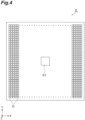
- the semiconductor light detection element 6 has a plurality of light detection units 10 disposed two-dimensionally and a common electrode E3.
- the semiconductor light detection element 6 has a rectangular shape when seen in the Z-axis direction, and the plurality of light detection units 10 are disposed in a matrix shape with the X-axis direction and the Y-axis direction as the row direction and the column direction.
- the common electrode E3 is located at the center of the semiconductor light detection element 6 when seen in the Z-axis direction. Electric charges generated in each light detection unit 10 are collected in the common electrode E3. That is, the semiconductor light detection element 6 is an SiPM having a plurality of SPADs (light detection units 10).
- the plurality of light detection units 10 are shown only in regions at both ends of the semiconductor light detection element 6, but the plurality of light detection units 10 are formed over the entire region of the semiconductor light detection element 6 except for the common electrode E3.
- each light detection unit 10 has an avalanche photodiode APD and a quenching resistor R1.
- One end of the quenching resistor R1 is electrically connected to the anode of the avalanche photodiode APD, and the other end of the quenching resistor R1 is electrically connected to the common electrode E3 via a readout wiring TL of the semiconductor light detection element 6. That is, the plurality of light detection units 10 are connected to each other in parallel, and in each light detection unit 10, the avalanche photodiode APD and the quenching resistor R1 are directly connected to each other. In the semiconductor light detection element 6, each avalanche photodiode APD is operated in Geiger mode.
- a reverse voltage (a reverse bias voltage) higher than a breakdown voltage of the avalanche photodiode APD is applied to the avalanche photodiode APD. That is, a potential V1 is applied to the anode of the avalanche photodiode APD, and a potential V2 which is positive with respect to the potential V1 is applied to the cathode of the avalanche photodiode APD.
- the polarities of these potentials are relative, and for example, one of the potentials may be a ground potential.
- the wiring substrate 5 is provided with a signal processing unit SP.
- the signal processing unit SP processes a signal output from each semiconductor light detection element 6 using each semiconductor light detection element 6 as a channel.
- the signal processing unit SP outputs the processed signal (the detection signal) to the control device 103 (see FIG. 1 ).
- the signal processing unit SP constitutes, for example, an application specific integrated circuit (ASIC).
- the signal processing unit SP may include a CMOS circuit that converts the signal output from each semiconductor light detection element 6 into a digital pulse.
- the readout wiring TL includes a plurality of signal lines TL1 and a plurality of signal lines TL2.
- each signal line TL1 extends in the Y-axis direction between the avalanche photodiodes APD adjacent in the X-axis direction
- each signal line TL2 extends in the X-axis direction between the avalanche photodiodes APD adjacent in the Y-axis direction.
- the plurality of signal lines TL1 and the plurality of signal lines TL2 extend in a grid pattern to be connected to each other at intersection points and are electrically connected to the common electrode E3.
- one end of the quenching resistor R1 is connected to an electrode E1, and the other end of the quenching resistor R1 is connected to the signal line TL1. That is, in each light detection unit 10, one end of the quenching resistor R1 is electrically connected to the anode of the avalanche photodiode APD via the electrode E1, and the other end of the quenching resistor R1 is electrically connected to the common electrode E3 via a readout wiring TL.
- the semiconductor light detection element 6 has a semiconductor layer 11.
- the semiconductor layer 11 includes an N-type (first conductivity type) semiconductor region (a first semiconductor region) 12, a P-type (second conductivity type) semiconductor region (a second semiconductor region) 13, and a plurality of P-type semiconductor regions (second semiconductor regions) 14.
- the semiconductor region 13 is formed on a surface of the semiconductor region 12 on the light incidence side.
- the plurality of semiconductor regions 14 are formed in the semiconductor region 13 along a surface of the semiconductor region 13 on the light incidence side.
- the impurity concentration of each semiconductor region 14 is higher than that of the semiconductor region 13.
- each avalanche photodiode APD is constituted by one semiconductor region 14 and regions of the semiconductor regions 12 and 13 overlapping the one semiconductor region 14 in the Z-axis direction. That is, each avalanche photodiode APD includes the N-type semiconductor region 12 and the P-type semiconductor regions 13 and 14 forming PN junctions with the N-type semiconductor region 12.
- the P-type semiconductor regions 13 and 14 are located on a side of a surface 6a of the semiconductor light detection element 6 with respect to the N-type semiconductor region 12.
- the surface 6a is a surface of the semiconductor light detection element 6 on the light incidence side.
- An insulating layer 16 is formed on a surface of the semiconductor region 13 on the light incidence side.
- the common electrode E3 and the readout wiring TL are disposed on the insulating layer 16.
- the common electrode E3 and the readout wiring TL are covered with an insulating layer 17.
- a surface of the insulating layer 17 on the light incidence side corresponds to the surface 6a of the semiconductor light detection element 6.
- one end of the quenching resistor R1 (see FIG. 6 ) is electrically connected to the semiconductor regions 13 and 14 of the avalanche photodiode APD, and the other end of the quenching resistor R1 is electrically connected to the readout wiring TL.
- a through hole TH is formed in the semiconductor layer 11.
- An insulating layer 18 is formed on an inner surface of the through hole TH and a surface of the semiconductor region 12 on a side opposite to the light incidence side.
- a through electrode TE is disposed on the inner surface of the through hole TH via the insulating layer 18.
- the through electrode TE is connected to the common electrode E3 at an opening of the through hole TH on the light incidence side.
- a bump electrode B1 is disposed on the through electrode TE via an under bump metal BM.
- the through electrode TE and the insulating layer 18 are covered with a passivation film PF.
- An N-type semiconductor region 1PC is formed in a region surrounding the through hole TH on the surface of the semiconductor region 12 on the light incidence side. The semiconductor region 1PC prevents the PN junction formed by the N-type semiconductor region 12 and the P-type semiconductor regions 13 and 14 from reaching the through hole TH.
- a groove is formed in the passivation film PF to surround the through hole TH when viewed in the Z-axis direction, and the semiconductor region 12 is exposed in the groove.
- a plurality of bump electrodes B2 are disposed on the semiconductor region 12 exposed in the groove.
- the bump electrode B1 and the plurality of bump electrodes B2 are electrically and physically connected to the wiring substrate 5 disposed on a side opposite to the plurality of metalenses 8 with respect to the semiconductor light detection element 6. That is, the semiconductor light detection element 6 is electrically and physically connected to the wiring substrate 5.
- the avalanche photodiode APD in each light detection unit 10 is operated in the Geiger mode. In this state, when light is incident on the semiconductor region 12 from a side of the surface 6a, photoelectric conversion occurs in the semiconductor region 12, and photoelectrons (electric charges) are generated in the semiconductor region 12. In the avalanche photodiode APD in which photoelectrons are generated, avalanche multiplication occurs in the semiconductor region 13, and an amplified electron group (electric charges) is collected in the common electrode E3 via the semiconductor region 14 and the quenching resistor R1. The electric charges collected in the common electrode E3 from each light detection unit 10 are input to the signal processing unit SP (see FIG. 5 ) of the wiring substrate 20 as a signal.
- the signal processing unit SP see FIG. 5
- the semiconductor layer 11 is made of Si, for example.
- the P-type impurities are, for example, Group 3 elements such as B
- the N-type impurities are, for example, Group 5 elements such as N, P, and As.
- a method of adding these impurities is, for example, a diffusion method or an ion injection method.
- Each insulating layer 16, 17, or 18 is made of, for example, SiO 2 or SiN.
- a method of forming each insulating layer 16, 17, or 18 is, for example, a thermal oxidation method or a sputtering method.
- the electrodes E1 and E3 and the through electrode TE are made of a metal such as aluminum, for example.
- a method of forming the electrodes E1 and E3 and the through electrode TE is, for example, a sputtering method.
- the resistivity of the quenching resistor R1 is higher than the resistivity of the electrode E1 and the resistivity of the common electrode E3.
- the quenching resistor R1 is made of polysilicon, for example.
- a method of forming the quenching resistor R1 is, for example, a chemical vapor deposition (CVD) method.
- the material of the quenching resistor R1 may be, for example, SiCr, NiCr, TaNi, FeCr, or the like.
- the plurality of metalenses 8 are provided on the light transmitting substrate 7.
- the plurality of metalenses 8 are disposed on the surface 6a of the semiconductor light detection element 6 via the light transmitting substrate 7.
- Each metalens 8 is two-dimensionally disposed to overlap each light detection unit 10 when viewed in the Z-axis direction (a direction intersecting with the surface 6a). That is, one metalens 8 corresponds to one light detection unit 10 (faces in the Z-axis direction).
- FIGS. 9 and 10 only a portion of the light detector 4 corresponding to one light detection unit 10 is illustrated.
- the plurality of metalenses 8 are metasurface lenses formed on a surface 7a of the light transmitting substrate 7.
- the light transmitting substrate 7 having the plurality of metalenses 8 formed on the surface 7a is bonded to the surface 6a of the semiconductor light detection element 6 with a light transmitting adhesive.
- the light transmitting substrate 7 is made of, for example, SiO 2 , GaAs, GaP, Si, SiC, or the like.
- the plurality of metalenses 8 are made of a metalens material such as a-Si, HfO 2 , Nb 2 O 5 , or TiO 2 , for example.
- the plurality of metalenses 8 are formed on the surface 7a of the light transmitting substrate 7 as follows.
- a film made of a metalens material is formed on the surface of the light transmitting substrate 7, an EB mask is formed on the film by an EB lithography method, and the film is subjected to an etching process, and thus the plurality of metalenses 8 are formed on the surface 7a of the light transmitting substrate 7.
- the metalens 8 is configured on the basis of the phase design of Fresnel lens, for example.
- the outer diameter of the metalens 8 is, for example, about 75 ⁇ m.
- the outer diameter of the metalens 8 is designed to correspond to the size of the light detection unit 10.
- the thickness of the metalens 8 in the Z-axis direction is, for example, about 500 nm.
- a single period of the metalens 8 is equal to or less than the wavelength of the light L, for example, about 250 nm.
- the thickness of the light transmitting substrate 7 is determined such that a convergence spot S, which will be described later, is located at a desired position.
- the thickness of the light transmitting substrate 7 is, for example, about several tens of ⁇ m.
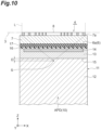
- the metalenses 8 converge the light L such that the convergence spot S is located at a position which is within the semiconductor region 12 and which is separated by a predetermined distance D from a boundary 15 between the semiconductor region 12 and the semiconductor region 13 in the Z-axis direction.
- the convergence spot S means a beam waist portion of the light L that has passed through the metalenses 8 (that is, a portion where the beam diameter of the light L is the smallest).
- the distance between the metalens 8 and the convergence spot S in the Z-axis direction is approximately 50 ⁇ m.
- each metalens 8 has a numerical aperture of ((0.61) 2 ⁇ ) 1/2 or more.
- NA the numerical aperture of the metalens 8
- the following expression (4) is derived from the above expressions (1), (2) and (3). As shown in FIG. 10 , since the light L is incident on the semiconductor layer 11 through the light transmitting substrate 7 and the insulating layers 16 and 17, strictly speaking, the effect of aberration occurs, but the expression (4) means that the Rayleigh length of the light L converged by the metalenses 8 is sufficiently shortened to about 1 ⁇ m or less. Z R ⁇ 1 ⁇ m
- the predetermined distance D is less than t/2. From another point of view, the predetermined distance D is 0 ⁇ m or more and 3 ⁇ m or less. This means that at least a region of the light L corresponding to the Rayleigh length Z R on the downstream side of the convergence spot S is located within the semiconductor region 12 in a case where the above expression (4) is satisfied (see FIGS. 10 and 11 ). This is because the convergence spot S is located on the boundary 15 between the semiconductor regions 12 and 13 in a case where the predetermined distance D is 0 ⁇ m.
- the predetermined distance D is 0 ⁇ or more and 3 ⁇ or less. This means that at least a region of the light L corresponding to the standard deviation ⁇ on the downstream side of the convergence spot S is located within the semiconductor region 12 (see FIGS. 10 and 11 ). This is because the convergence spot S is located on the boundary 15 between the semiconductor regions 12 and 13 in a case where the predetermined distance D is 0 ⁇ .
- the predetermined distance D is 1 ⁇ m or more in a case where the above expression (4) is satisfied means that a region of the light L corresponding to the Rayleigh length Z R on the upstream side of the convergence spot S is located within the semiconductor region 12.
- the fact that the predetermined distance D is ⁇ or more in a case where the above expression (4) is satisfied means that a region of the light L corresponding to the Rayleigh length Z R on the upstream side of the convergence spot S is located within the semiconductor region 12.
- the metalenses 8 converge the light L such that the convergence spot S is located at a position which is within the semiconductor region 12 of each light detection unit 10 and which is separated by a predetermined distance D from a boundary 15 between the semiconductor region 12 and the semiconductor region 13 in the Z-axis direction.
- the depth of the portion in the semiconductor region 12 where electric charges are generated is uniformized among the plurality of light detection units 10. Therefore, according to the light detector 4, the response time (a time from the generation of the electric charges to the detection of the electric charges) can be sufficiently uniformized.
- the plurality of metalenses 8 have an excellent effect as compared with, for example, a resin-made microlens array. That is, since the plurality of metalenses 8 are formed of an inorganic substance with a thickness equal to or less than the wavelength of the light L, the plurality of metalenses 8 are physically and chemically stable. In particular, since the scintillator 3 is disposed on the plurality of metalenses 8, the metalenses 8 that are difficult to be deformed by the weight of the scintillator 3 are extremely effective in reliably locating the convergence spot S at a position separated by the predetermined distance D from the boundary 15 between the semiconductor region 12 and the semiconductor region 13. The metalens 8 also has the same effect in that it is difficult to deform due to heat. Further, according to the metalens 8, it is possible to design the phase of the lens by controlling a two-dimensional shape, and it is also possible to realize a high numerical aperture.
- the predetermined distance D is less than t/2.
- the predetermined distance D is 0 ⁇ or more and 3 ⁇ or less.
- each metalens 8 has a numerical aperture of ((0.61) 2 ⁇ ) 1/2 or more.
- the Rayleigh length of the light L converged by the metalenses 8 is sufficiently shortened to about 1 ⁇ m or less, and thus it is possible to more reliably curb variations in response time.
- the predetermined distance D is 0 ⁇ m or more and 3 ⁇ m or less.
- the plurality of metalenses 8 are provided on the light transmitting substrate 7 and disposed on the surface 6a of the semiconductor light detection element 6 via the light transmitting substrate 7.
- the light transmitting substrate 7 it is possible to improve the yield of the light detector 4 by bonding the light transmitting substrate 7 on which the plurality of metalenses 8 are formed to the surface 6a of the semiconductor light detection element 6.
- the light transmitting substrate 7 function as a spacer between the metalenses 8 and the light detection unit 10, and it is possible to reliably locate the convergence spot S at a position separated by the predetermined distance D from the boundary 15 between the semiconductor region 12 and the semiconductor region 13.
- the wiring substrate 5 is disposed on a side opposite to the plurality of metalenses 8 with respect to the semiconductor light detection element 6, and the semiconductor light detection element 6 is electrically and physically connected to the wiring substrate 5.
- an external wiring can be connected to the wiring substrate 5 from a side opposite to the plurality of metalenses 8.
- the radiation detector 2 it is possible to sufficiently uniformize the response time in the light detector 4 for the reasons described above.
- the PET device 1 it is possible to sufficiently uniformize the response time in the plurality of light detectors 4 for the reasons described above, and thus it is possible to acquire a high-quality image.
- FIG. 12 is a graph showing time resolution of light detectors of an example and a comparative example.
- a horizontal axis indicates the response time in the light detectors of the example and the comparative example
- a vertical axis indicates a normalized count number (a normalized count number of the detection signal) in the light detectors of the example and the comparative example.
- a dashed line indicates the time resolution of the light detector of the example
- a solid line indicates the time resolution of the light detector of the comparative example.
- the light detector of the example a light detector having the same configuration as the light detector 4 of the above embodiment was used.
- the light detector of the comparative example a light detector having a configuration in which the light transmitting substrate 7 and the plurality of metalens 8 are removed from the light detector 4 of the above embodiment was used. As shown in FIG. 12 , the half width of the time resolution in the light detector of the example was smaller than the half width of the time resolution in the light detector of the comparative example.
- the plurality of metalens 8 may be disposed directly on the surface 6a of the semiconductor light detection element 6. Moreover, the plurality of metalenses 8 may be configured by forming grooves on the surface 7a of the light transmitting substrate 7. Further, the semiconductor light detection element 6 as a SiPM having a plurality of SPADs (light detection units 10) may have other configurations such as a configuration in which N-type and P-type are reversed. Further, a detection target of the radiation detector 2 is not limited to an annihilation ⁇ ray and may be another radiation such as an X ray. In the radiation detector 2, the light emitting body that emits light upon incidence of radiation is not limited to the scintillator 3 and may be another light emitting body such as Cherenkov radiator.
Landscapes
- Physics & Mathematics (AREA)
- Health & Medical Sciences (AREA)
- Life Sciences & Earth Sciences (AREA)
- General Physics & Mathematics (AREA)
- High Energy & Nuclear Physics (AREA)
- Molecular Biology (AREA)
- Spectroscopy & Molecular Physics (AREA)
- Engineering & Computer Science (AREA)
- Microelectronics & Electronic Packaging (AREA)
- Light Receiving Elements (AREA)
- Nuclear Medicine (AREA)
- Measurement Of Radiation (AREA)
Abstract
Description
- The present disclosure relates to a light detector, a radiation detector, and a PET device.
- A time-of-flight positron emission tomography (TOF-PET) device has a plurality of radiation detectors disposed in an annular shape, and each radiation detector includes a light emitting body (a scintillator, Cherenkov radiator, or the like) that emits light upon incidence of radiation and a light detector that detects the light emitted by the light emitting body. In order to acquire a high-quality image in a TOF-PET device, it is necessary to uniformize time from generation of electric charges to detection of the electric charges (hereinafter referred to as "response time") and to improve single photon time resolution in a light detector of each radiation detector.
-
Patent Literature 1 describes a light detection device that includes a silicon photo multiplier (SiPM) having a plurality of single photon avalanche diodes (SPADs) and a plurality of microlenses disposed on a surface of the SiPM. In the light detection device disclosed inPatent Literature 1, in order to uniformize response time of each SPAD, a generation position of electric charges in each SPAD is controlled in a direction parallel to a surface of an SiPM by a plurality of microlenses. - [Patent Literature 1]
Japanese Unexamined Patent Publication No. 2020-115575 - Although the light detection device described in
Patent Literature 1 is applied to each radiation detector of a TOF-PET device and a generation position of electric charges in each SPAD is controlled in a direction parallel to a surface of an SiPM by a plurality of microlenses, it cannot be said that response time can be sufficiently uniformized in each SPAD from the viewpoint of improving single-photon time resolution. - An object of the present disclosure is to provide a light detector capable of sufficiently uniformizing response time, and a radiation detector and a PET device including such a light detector.
- According to an aspect of the present disclosure, there is provided a light detector including: a semiconductor light detection element having a plurality of light detection units disposed two-dimensionally and readout wirings; and a plurality of metalenses disposed on a surface of the semiconductor light detection element, wherein each of the plurality of light detection units has an avalanche photodiode including a first semiconductor region of a first conductivity type and a second semiconductor region of a second conductivity type, the second semiconductor region located on a side of the surface with respect to the first semiconductor region and forming a PN junction with the first semiconductor region, and a quenching resistor including one end electrically connected to the second semiconductor region and another end electrically connected to the readout wiring, and wherein the plurality of metalenses are disposed two-dimensionally to overlap the plurality of light detection units when seen in a direction intersecting with the surface, and converge light such that a convergence spot is located at a position which is within the first semiconductor region of each of the plurality of light detection units and which is separated by a predetermined distance from a boundary between the first semiconductor region and the second semiconductor region in the direction intersecting with the surface.
- In the light detector according to the aspect of the present disclosure, the metalenses converge the light such that the convergence spot is located at a position which is within the first semiconductor region of each of the plurality of light detection units and which is separated by a predetermined distance from the boundary between the first semiconductor region and the second semiconductor region in the direction intersecting with the surface. As a result, the depth of the portion in the first semiconductor region where electric charges are generated is uniformized among the plurality of light detection units. Therefore, according to the light detector of the aspect of the present disclosure, the response time can be sufficiently uniformized.
- In the light detector according to the aspect of the present disclosure, when a thickness of the first semiconductor region in the direction intersecting with the surface is defined as t, the predetermined distance may be less than t/2. According to this, the portion where the electric charges are generated in the first semiconductor region is sufficiently close to the second semiconductor region, and thus it is possible to more reliably curb variations in response time.
- In the light detector according to the aspect of the present disclosure, when a standard deviation of a Gaussian function in a case where a beam profile of the convergence spot in the direction intersecting with the surface is approximated to the Gaussian function is defined as σ, the predetermined distance may be 0σ or more and 3σ or less. According to this, the portion where the electric charges are generated in the first semiconductor region is sufficiently close to the second semiconductor region, and thus it is possible to more reliably curb variations in response time.
- In the light detector according to the aspect of the present disclosure, when a wavelength of the light is defined as λ (µm), each of the plurality of metalenses may have a numerical aperture of ((0.61)2πλ)1/2 or more. According to this, the Rayleigh length of the light converged by the metalenses is sufficiently shortened to about 1 µm or less, and thus it is possible to more reliably curb variations in response time.
- In the light detector according to the aspect of the present disclosure, the predetermined distance may be 0 µm or more and 3 µm or less. According to this, the portion where the electric charges are generated in the first semiconductor region is sufficiently close to the second semiconductor region, and thus it is possible to more reliably curb variations in response time.
- The light detector according to the aspect of the present disclosure may further include a light transmitting substrate provided with the plurality of metalenses, wherein the plurality of metalenses may be disposed on the surface of the semiconductor light detection element via the light transmitting substrate. According to this, in manufacturing the light detector, for example, it is possible to improve the yield of the light detector by bonding the light transmitting substrate on which the plurality of metalenses are formed to the surface of the semiconductor light detection element. In addition, it is possible to make the light transmitting substrate function as a spacer between the metalenses and the light detection unit, and it is possible to reliably locate the convergence spot at a position separated by the predetermined distance from the boundary between the first semiconductor region and the second semiconductor region.
- The light detector according to the aspect of the present disclosure may further include a wiring substrate disposed on a side opposite to the plurality of metalenses with respect to the semiconductor light detection element, wherein the semiconductor light detection element may be electrically and physically connected to the wiring substrate. According to this, an external wiring can be connected to the wiring substrate from a side opposite to the plurality of metalenses.
- According to an aspect of the present disclosure, there is provided a radiation detector including: a light emitting body configured to emit light upon incidence of radiation; and the light detector described above, wherein the light emitting body is disposed on a side opposite to the semiconductor light detection element with respect to the plurality of metalenses.
- According to the radiation detector of the aspect of the present disclosure, it is possible to sufficiently uniformize the response time in the light detector for the reasons described above.
- According to an aspect of the present disclosure, there is provided a PET device including: a plurality of radiation detectors disposed in an annular shape, wherein each of the plurality of radiation detectors is the radiation detector described above.
- According to the PET device of the aspect of the present disclosure, it is possible to sufficiently uniformize the response time in the plurality of light detectors for the reasons described above, and thus it is possible to acquire a high-quality image.
- According to the present disclosure, it is possible to provide a light detector capable of sufficiently uniformizing response time, and a radiation detector and a PET device including such a light detector.
-
-
FIG. 1 is a configuration diagram of a PET device of an embodiment. -
FIG. 2 is a configuration diagram of a radiation detection device shown inFIG. 1 . -
FIG. 3 is a side view of a radiation detector shown inFIG. 2 . -
FIG. 4 is a plan view of a semiconductor light detection element shown inFIG. 3 . -
FIG. 5 is a circuit diagram of a light detector shown inFIG. 3 . -
FIG. 6 is a plan view of a portion of the semiconductor light detection element shown inFIG. 4 . -
FIG. 7 is a cross-sectional view of a portion of the semiconductor light detection element shown inFIG. 4 . -
FIG. 8 is a bottom view of the semiconductor light detection element shown inFIG. 4 . -
FIG. 9 is a plan view of a portion of the light detector shown inFIG. 3 . -
FIG. 10 is a cross-sectional view of a portion of the light detector along line X-X shown inFIG. 9 . -
FIG. 11 is a diagram showing a convergence state of light shown inFIG. 10 . -
FIG. 12 is a graph showing time resolution of light detectors of an example and a comparative example. -
FIG. 13 is a cross-sectional view of a portion of a light detector of a modification example. - Hereinafter, an embodiment of the present disclosure will be described in detail with reference to the drawings. The same or corresponding parts in the drawings are denoted with the same reference signs, and repetitive description will be omitted.
- As shown in
FIG. 1 , thePET device 1 includes acradle 101, agantry 102, acontrol device 103, and adrive motor 104. Thecradle 101 is disposed to pass through an opening in thegantry 102. Asubject 105 is placed on thecradle 101. Thecontrol device 103 controls thedrive motor 104 according to a drive motor control signal. As a result, thecradle 101 on which thesubject 105 is placed moves, and the relative position of thesubject 105 with respect to the opening of thegantry 102 changes. Thedrive motor 104 may be configured to move thegantry 102 or may be configured to move thecradle 101 and thegantry 102. - The
gantry 102 has a plurality ofradiation detection devices 106. The plurality ofradiation detection devices 106 are disposed in a direction in which the opening of thegantry 102 penetrates. Theradiation detection devices 106 surround the opening of thegantry 102. Thecontrol device 103 inputs a control signal for controlling eachradiation detection device 106 to thegantry 102. Thegantry 102 outputs a detection signal detected by eachradiation detection device 106 to thecontrol device 103. - As shown in
FIG. 2 , theradiation detection device 106 includes a plurality ofradiation detectors 2. The plurality ofradiation detectors 2 are disposed in an annular shape to surround the opening of thegantry 102. The subject 105 is injected with a radioisotope (a positron emitting nuclide) that emits positrons. Positrons combine with negative electrons in the subject 105 to generate annihilation γ rays. The annihilation γ rays are emitted in opposite directions from a position P of the radioisotope within the subject 105. As a result, the annihilation γ rays are detected by a pair ofradiation detectors 2 facing each other with the position P interposed therebetween. Thecontrol device 103 identifies the position P on the basis of a time-of-flight difference of the annihilation γ rays and generates an image (a tomographic image) regarding internal information of the subject 105. In other words, thePET device 1 is a TOF-PET device. - As shown in
FIG. 3 , theradiation detector 2 includes a plurality ofradiation detection units 2A. The plurality ofradiation detection units 2A are disposed in a matrix shape with an X-axis direction and a Y-axis direction as a row direction and a column direction. Eachradiation detection unit 2A includes a scintillator (a light emitting body) 3 and alight detector 4. InFIG. 3 , a Z-axis direction is a radial direction of an annulus (seeFIG. 2 ) in which the plurality ofradiation detectors 2 are disposed, an X-axis direction is a tangential direction of the annulus, and a Y-axis direction is a direction perpendicular to the Z-axis direction and the X-axis direction. - The
scintillator 3 is disposed on the center side of the opening of the gantry 102 (hereinafter referred to as a "light incidence side") with respect to the light detector 4 (seeFIG. 2 ). Thescintillator 3 emits light (fluorescence) upon incidence of annihilation γ rays. Thescintillator 3 is formed of at least one material or a mixture of a plurality of materials selected from the group consisting of Lu2-xYxSiO5:Ce(LYSO), gadolinium aluminum gallium garnet (GAGG), NaI(TI), Pr:LuAG, LaBr2, LaBr3, and (LuxTb1-x-yCey)3Al5O12 (that is, LuTAG). In LuTAG, a composition ratio x is in the range of 0.5 to 1.5, and a composition ratio y is in the range of 0.01 to 0.15. - The
light detector 4 detects the light emitted from thescintillator 3. Thelight detector 4 has awiring substrate 5, a semiconductorlight detection element 6, alight transmitting substrate 7, and a plurality ofmetalenses 8. Thewiring substrate 5 is shared by a plurality oflight detectors 4. Thewiring substrate 5, the semiconductorlight detection element 6, thelight transmitting substrate 7, and the plurality ofmetalenses 8 are disposed in that order from a side opposite to thescintillator 3. That is, thescintillator 3 is disposed on a side opposite to the semiconductorlight detection element 6 with respect to the plurality ofmetalenses 8. Thescintillator 3 is bonded to thelight detector 4 with a light transmitting adhesive. - As shown in
FIG. 4 , the semiconductorlight detection element 6 has a plurality oflight detection units 10 disposed two-dimensionally and a common electrode E3. As an example, the semiconductorlight detection element 6 has a rectangular shape when seen in the Z-axis direction, and the plurality oflight detection units 10 are disposed in a matrix shape with the X-axis direction and the Y-axis direction as the row direction and the column direction. The common electrode E3 is located at the center of the semiconductorlight detection element 6 when seen in the Z-axis direction. Electric charges generated in eachlight detection unit 10 are collected in the common electrode E3. That is, the semiconductorlight detection element 6 is an SiPM having a plurality of SPADs (light detection units 10). InFIG. 4 , the plurality oflight detection units 10 are shown only in regions at both ends of the semiconductorlight detection element 6, but the plurality oflight detection units 10 are formed over the entire region of the semiconductorlight detection element 6 except for the common electrode E3. - As shown in
FIG. 5 , eachlight detection unit 10 has an avalanche photodiode APD and a quenching resistor R1. One end of the quenching resistor R1 is electrically connected to the anode of the avalanche photodiode APD, and the other end of the quenching resistor R1 is electrically connected to the common electrode E3 via a readout wiring TL of the semiconductorlight detection element 6. That is, the plurality oflight detection units 10 are connected to each other in parallel, and in eachlight detection unit 10, the avalanche photodiode APD and the quenching resistor R1 are directly connected to each other. In the semiconductorlight detection element 6, each avalanche photodiode APD is operated in Geiger mode. In the Geiger mode, a reverse voltage (a reverse bias voltage) higher than a breakdown voltage of the avalanche photodiode APD is applied to the avalanche photodiode APD. That is, a potential V1 is applied to the anode of the avalanche photodiode APD, and a potential V2 which is positive with respect to the potential V1 is applied to the cathode of the avalanche photodiode APD. The polarities of these potentials are relative, and for example, one of the potentials may be a ground potential. - The
wiring substrate 5 is provided with a signal processing unit SP. The signal processing unit SP processes a signal output from each semiconductorlight detection element 6 using each semiconductorlight detection element 6 as a channel. The signal processing unit SP outputs the processed signal (the detection signal) to the control device 103 (seeFIG. 1 ). The signal processing unit SP constitutes, for example, an application specific integrated circuit (ASIC). The signal processing unit SP may include a CMOS circuit that converts the signal output from each semiconductorlight detection element 6 into a digital pulse. - As shown in
FIG. 6 , in the semiconductorlight detection element 6, the readout wiring TL includes a plurality of signal lines TL1 and a plurality of signal lines TL2. As an example, each signal line TL1 extends in the Y-axis direction between the avalanche photodiodes APD adjacent in the X-axis direction, and each signal line TL2 extends in the X-axis direction between the avalanche photodiodes APD adjacent in the Y-axis direction. The plurality of signal lines TL1 and the plurality of signal lines TL2 extend in a grid pattern to be connected to each other at intersection points and are electrically connected to the common electrode E3. - In each
light detection unit 10, one end of the quenching resistor R1 is connected to an electrode E1, and the other end of the quenching resistor R1 is connected to the signal line TL1. That is, in eachlight detection unit 10, one end of the quenching resistor R1 is electrically connected to the anode of the avalanche photodiode APD via the electrode E1, and the other end of the quenching resistor R1 is electrically connected to the common electrode E3 via a readout wiring TL. - As shown in
FIG. 7 , the semiconductorlight detection element 6 has asemiconductor layer 11. Thesemiconductor layer 11 includes an N-type (first conductivity type) semiconductor region (a first semiconductor region) 12, a P-type (second conductivity type) semiconductor region (a second semiconductor region) 13, and a plurality of P-type semiconductor regions (second semiconductor regions) 14. Thesemiconductor region 13 is formed on a surface of thesemiconductor region 12 on the light incidence side. The plurality ofsemiconductor regions 14 are formed in thesemiconductor region 13 along a surface of thesemiconductor region 13 on the light incidence side. The impurity concentration of eachsemiconductor region 14 is higher than that of thesemiconductor region 13. - In the semiconductor
light detection element 6, one avalanche photodiode APD is constituted by onesemiconductor region 14 and regions of thesemiconductor regions semiconductor region 14 in the Z-axis direction. That is, each avalanche photodiode APD includes the N-type semiconductor region 12 and the P-type semiconductor regions type semiconductor region 12. The P-type semiconductor regions surface 6a of the semiconductorlight detection element 6 with respect to the N-type semiconductor region 12. Thesurface 6a is a surface of the semiconductorlight detection element 6 on the light incidence side. - An insulating
layer 16 is formed on a surface of thesemiconductor region 13 on the light incidence side. The common electrode E3 and the readout wiring TL are disposed on the insulatinglayer 16. The common electrode E3 and the readout wiring TL are covered with an insulatinglayer 17. In the semiconductorlight detection element 6, a surface of the insulatinglayer 17 on the light incidence side corresponds to thesurface 6a of the semiconductorlight detection element 6. In eachlight detection unit 10, one end of the quenching resistor R1 (seeFIG. 6 ) is electrically connected to thesemiconductor regions - A through hole TH is formed in the
semiconductor layer 11. An insulatinglayer 18 is formed on an inner surface of the through hole TH and a surface of thesemiconductor region 12 on a side opposite to the light incidence side. A through electrode TE is disposed on the inner surface of the through hole TH via the insulatinglayer 18. The through electrode TE is connected to the common electrode E3 at an opening of the through hole TH on the light incidence side. A bump electrode B1 is disposed on the through electrode TE via an under bump metal BM. The through electrode TE and the insulatinglayer 18 are covered with a passivation film PF. An N-type semiconductor region 1PC is formed in a region surrounding the through hole TH on the surface of thesemiconductor region 12 on the light incidence side. The semiconductor region 1PC prevents the PN junction formed by the N-type semiconductor region 12 and the P-type semiconductor regions - As shown in
FIG. 8 , a groove is formed in the passivation film PF to surround the through hole TH when viewed in the Z-axis direction, and thesemiconductor region 12 is exposed in the groove. A plurality of bump electrodes B2 are disposed on thesemiconductor region 12 exposed in the groove. The bump electrode B1 and the plurality of bump electrodes B2 are electrically and physically connected to thewiring substrate 5 disposed on a side opposite to the plurality ofmetalenses 8 with respect to the semiconductorlight detection element 6. That is, the semiconductorlight detection element 6 is electrically and physically connected to thewiring substrate 5. - In the semiconductor
light detection element 6 configured as described above, the avalanche photodiode APD in eachlight detection unit 10 is operated in the Geiger mode. In this state, when light is incident on thesemiconductor region 12 from a side of thesurface 6a, photoelectric conversion occurs in thesemiconductor region 12, and photoelectrons (electric charges) are generated in thesemiconductor region 12. In the avalanche photodiode APD in which photoelectrons are generated, avalanche multiplication occurs in thesemiconductor region 13, and an amplified electron group (electric charges) is collected in the common electrode E3 via thesemiconductor region 14 and the quenching resistor R1. The electric charges collected in the common electrode E3 from eachlight detection unit 10 are input to the signal processing unit SP (seeFIG. 5 ) of the wiring substrate 20 as a signal. - The
semiconductor layer 11 is made of Si, for example. In thesemiconductor layer 11, the P-type impurities are, for example,Group 3 elements such as B, and the N-type impurities are, for example,Group 5 elements such as N, P, and As. A method of adding these impurities is, for example, a diffusion method or an ion injection method. Each insulatinglayer layer - As shown in
FIGS. 3 ,9 and10 , the plurality ofmetalenses 8 are provided on thelight transmitting substrate 7. The plurality ofmetalenses 8 are disposed on thesurface 6a of the semiconductorlight detection element 6 via thelight transmitting substrate 7. Eachmetalens 8 is two-dimensionally disposed to overlap eachlight detection unit 10 when viewed in the Z-axis direction (a direction intersecting with thesurface 6a). That is, onemetalens 8 corresponds to one light detection unit 10 (faces in the Z-axis direction). InFIGS. 9 and10 , only a portion of thelight detector 4 corresponding to onelight detection unit 10 is illustrated. - The plurality of
metalenses 8 are metasurface lenses formed on asurface 7a of thelight transmitting substrate 7. Thelight transmitting substrate 7 having the plurality ofmetalenses 8 formed on thesurface 7a is bonded to thesurface 6a of the semiconductorlight detection element 6 with a light transmitting adhesive. Thelight transmitting substrate 7 is made of, for example, SiO2, GaAs, GaP, Si, SiC, or the like. The plurality ofmetalenses 8 are made of a metalens material such as a-Si, HfO2, Nb2O5, or TiO2, for example. As an example, the plurality ofmetalenses 8 are formed on thesurface 7a of thelight transmitting substrate 7 as follows. That is, a film made of a metalens material is formed on the surface of thelight transmitting substrate 7, an EB mask is formed on the film by an EB lithography method, and the film is subjected to an etching process, and thus the plurality ofmetalenses 8 are formed on thesurface 7a of thelight transmitting substrate 7. - The
metalens 8 is configured on the basis of the phase design of Fresnel lens, for example. The outer diameter of themetalens 8 is, for example, about 75 µm. The outer diameter of themetalens 8 is designed to correspond to the size of thelight detection unit 10. The thickness of themetalens 8 in the Z-axis direction is, for example, about 500 nm. A single period of themetalens 8 is equal to or less than the wavelength of the light L, for example, about 250 nm. The thickness of thelight transmitting substrate 7 is determined such that a convergence spot S, which will be described later, is located at a desired position. The thickness of thelight transmitting substrate 7 is, for example, about several tens of µm. - As shown in
FIG. 10 , in themetalenses 8 and thelight detection unit 10 facing each other in the Z-axis direction, themetalenses 8 converge the light L such that the convergence spot S is located at a position which is within thesemiconductor region 12 and which is separated by a predetermined distance D from aboundary 15 between thesemiconductor region 12 and thesemiconductor region 13 in the Z-axis direction. The convergence spot S means a beam waist portion of the light L that has passed through the metalenses 8 (that is, a portion where the beam diameter of the light L is the smallest). The distance between themetalens 8 and the convergence spot S in the Z-axis direction is approximately 50 µm. - Here, when a wavelength of the light L is defined as λ (µm), each
metalens 8 has a numerical aperture of ((0.61)2πλ)1/2 or more. In other words, when the numerical aperture of themetalens 8 is defined as NA, the following expression (1) is satisfied.
- Further, as shown in
FIG. 11 , when Rayleigh length of the light L converged by themetalenses 8 is defined as ZR (µm) and a beam waist is defined as ω0 (µm), the following expressions (2) and (3) are satisfied.

- The following expression (4) is derived from the above expressions (1), (2) and (3). As shown in
FIG. 10 , since the light L is incident on thesemiconductor layer 11 through thelight transmitting substrate 7 and the insulatinglayers metalenses 8 is sufficiently shortened to about 1 µm or less.
- Further, when a thickness of the
semiconductor region 12 in the Z-axis direction is defined as t, the predetermined distance D is less than t/2. From another point of view, the predetermined distance D is 0 µm or more and 3 µm or less. This means that at least a region of the light L corresponding to the Rayleigh length ZR on the downstream side of the convergence spot S is located within thesemiconductor region 12 in a case where the above expression (4) is satisfied (seeFIGS. 10 and11 ). This is because the convergence spot S is located on theboundary 15 between thesemiconductor regions FIGS. 10 and11 ). This is because the convergence spot S is located on theboundary 15 between thesemiconductor regions light detector 4, photoelectric conversion occurs at a portion in the vicinity of thesemiconductor region 13 in thesemiconductor region 12 in eachlight detection unit 10, and electric charges are likely to be generated in this region. The fact that the predetermined distance D is 1 µm or more in a case where the above expression (4) is satisfied means that a region of the light L corresponding to the Rayleigh length ZR on the upstream side of the convergence spot S is located within thesemiconductor region 12. Similarly, the fact that the predetermined distance D is σ or more in a case where the above expression (4) is satisfied means that a region of the light L corresponding to the Rayleigh length ZR on the upstream side of the convergence spot S is located within thesemiconductor region 12. - As described above, in the
light detector 4, themetalenses 8 converge the light L such that the convergence spot S is located at a position which is within thesemiconductor region 12 of eachlight detection unit 10 and which is separated by a predetermined distance D from aboundary 15 between thesemiconductor region 12 and thesemiconductor region 13 in the Z-axis direction. As a result, the depth of the portion in thesemiconductor region 12 where electric charges are generated is uniformized among the plurality oflight detection units 10. Therefore, according to thelight detector 4, the response time (a time from the generation of the electric charges to the detection of the electric charges) can be sufficiently uniformized. - The plurality of
metalenses 8 have an excellent effect as compared with, for example, a resin-made microlens array. That is, since the plurality ofmetalenses 8 are formed of an inorganic substance with a thickness equal to or less than the wavelength of the light L, the plurality ofmetalenses 8 are physically and chemically stable. In particular, since thescintillator 3 is disposed on the plurality ofmetalenses 8, themetalenses 8 that are difficult to be deformed by the weight of thescintillator 3 are extremely effective in reliably locating the convergence spot S at a position separated by the predetermined distance D from theboundary 15 between thesemiconductor region 12 and thesemiconductor region 13. Themetalens 8 also has the same effect in that it is difficult to deform due to heat. Further, according to themetalens 8, it is possible to design the phase of the lens by controlling a two-dimensional shape, and it is also possible to realize a high numerical aperture. - In the
light detector 4, when a thickness of thesemiconductor region 12 in the Z-axis direction is defined as t, the predetermined distance D is less than t/2. As a result, the portion where the electric charges are generated in thesemiconductor region 12 is sufficiently close to thesemiconductor region 13, and thus it is possible to more reliably curb variations in response time. - In the
light detector 4, when a standard deviation of the Gaussian function in a case where a beam profile of the convergence spot S in the Z-axis direction is approximated to the Gaussian function is defined as σ, the predetermined distance D is 0σ or more and 3σ or less. As a result, the portion where the electric charges are generated in thesemiconductor region 12 is sufficiently close to thesemiconductor region 13, and thus it is possible to more reliably curb variations in response time. - In the
light detector 4, when a wavelength of the light L is defined as λ (µm), eachmetalens 8 has a numerical aperture of ((0.61)2πλ)1/2 or more. As a result, the Rayleigh length of the light L converged by themetalenses 8 is sufficiently shortened to about 1 µm or less, and thus it is possible to more reliably curb variations in response time. - In the
light detector 4, the predetermined distance D is 0 µm or more and 3 µm or less. As a result, the portion where the electric charges are generated in thesemiconductor region 12 is sufficiently close to thesemiconductor region 13, and thus it is possible to more reliably curb variations in response time. - In the
light detector 4, the plurality ofmetalenses 8 are provided on thelight transmitting substrate 7 and disposed on thesurface 6a of the semiconductorlight detection element 6 via thelight transmitting substrate 7. As a result, in manufacturing thelight detector 4, for example, it is possible to improve the yield of thelight detector 4 by bonding thelight transmitting substrate 7 on which the plurality ofmetalenses 8 are formed to thesurface 6a of the semiconductorlight detection element 6. In addition, it is possible to make thelight transmitting substrate 7 function as a spacer between themetalenses 8 and thelight detection unit 10, and it is possible to reliably locate the convergence spot S at a position separated by the predetermined distance D from theboundary 15 between thesemiconductor region 12 and thesemiconductor region 13. - In the
light detector 4, thewiring substrate 5 is disposed on a side opposite to the plurality ofmetalenses 8 with respect to the semiconductorlight detection element 6, and the semiconductorlight detection element 6 is electrically and physically connected to thewiring substrate 5. As a result, an external wiring can be connected to thewiring substrate 5 from a side opposite to the plurality ofmetalenses 8. - According to the
radiation detector 2, it is possible to sufficiently uniformize the response time in thelight detector 4 for the reasons described above. - According to the
PET device 1, it is possible to sufficiently uniformize the response time in the plurality oflight detectors 4 for the reasons described above, and thus it is possible to acquire a high-quality image. -
FIG. 12 is a graph showing time resolution of light detectors of an example and a comparative example. In the graph shown inFIG. 12 , a horizontal axis indicates the response time in the light detectors of the example and the comparative example, and a vertical axis indicates a normalized count number (a normalized count number of the detection signal) in the light detectors of the example and the comparative example. In the graph shown inFIG. 12 , a dashed line indicates the time resolution of the light detector of the example, and a solid line indicates the time resolution of the light detector of the comparative example. As the light detector of the example, a light detector having the same configuration as thelight detector 4 of the above embodiment was used. As the light detector of the comparative example, a light detector having a configuration in which thelight transmitting substrate 7 and the plurality ofmetalens 8 are removed from thelight detector 4 of the above embodiment was used. As shown inFIG. 12 , the half width of the time resolution in the light detector of the example was smaller than the half width of the time resolution in the light detector of the comparative example. - The present disclosure is not limited to the above embodiment. For example, as shown in
FIG. 13 , the plurality ofmetalens 8 may be disposed directly on thesurface 6a of the semiconductorlight detection element 6. Moreover, the plurality ofmetalenses 8 may be configured by forming grooves on thesurface 7a of thelight transmitting substrate 7. Further, the semiconductorlight detection element 6 as a SiPM having a plurality of SPADs (light detection units 10) may have other configurations such as a configuration in which N-type and P-type are reversed. Further, a detection target of theradiation detector 2 is not limited to an annihilation γ ray and may be another radiation such as an X ray. In theradiation detector 2, the light emitting body that emits light upon incidence of radiation is not limited to thescintillator 3 and may be another light emitting body such as Cherenkov radiator. -
- 1 PET device
- 2 Radiation detector
- 3 Scintillator (light emitting body)
- 4 Light detector
- 5 Wiring substrate
- 6 Semiconductor light detection element
- 6a Surface
- 7 Light transmitting substrate
- 8 Metalens
- 10 Light detection unit
- 12 Semiconductor region (first semiconductor region)
- 13, 14 Semiconductor region (second semiconductor region)
- 15 Boundary
- APD Avalanche photodiode
- R1 Quenching resistor
- TL Readout wiring
- L Light
- S Convergence spot
Claims (9)
- A light detector comprising:a semiconductor light detection element having a plurality of light detection units disposed two-dimensionally and readout wirings; anda plurality of metalenses disposed on a surface of the semiconductor light detection element,wherein each of the plurality of light detection units hasan avalanche photodiode including a first semiconductor region of a first conductivity type and a second semiconductor region of a second conductivity type, the second semiconductor region located on a side of the surface with respect to the first semiconductor region and forming a PN junction with the first semiconductor region, anda quenching resistor including one end electrically connected to the second semiconductor region and another end electrically connected to the readout wiring, andwherein the plurality of metalenses are disposed two-dimensionally to overlap the plurality of light detection units when seen in a direction intersecting with the surface, and converge light such that a convergence spot is located at a position which is within the first semiconductor region of each of the plurality of light detection units and which is separated by a predetermined distance from a boundary between the first semiconductor region and the second semiconductor region in the direction intersecting with the surface.
- The light detector according to claim 1, wherein, when a thickness of the first semiconductor region in the direction intersecting with the surface is defined as t, the predetermined distance is less than t/2.
- The light detector according to claim 1 or 2, wherein, when a standard deviation of a Gaussian function in a case where a beam profile of the convergence spot in the direction intersecting with the surface is approximated to the Gaussian function is defined as σ, the predetermined distance is 0σ or more and 3σ or less.
- The light detector according to any one of claims 1 to 3, wherein, when a wavelength of the light is defined as λ (µm), each of the plurality of metalenses has a numerical aperture of ((0.61)2πλ)1/2 or more.
- The light detector according to claim 4, wherein the predetermined distance is 0 µm or more and 3 µm or less.
- The light detector according to any one of claims 1 to 5, further comprising:a light transmitting substrate provided with the plurality of metalenses,wherein the plurality of metalenses are disposed on the surface of the semiconductor light detection element via the light transmitting substrate.
- The light detector according to any one of claims 1 to 6, further comprising:a wiring substrate disposed on a side opposite to the plurality of metalenses with respect to the semiconductor light detection element,wherein the semiconductor light detection element is electrically and physically connected to the wiring substrate.
- A radiation detector comprising:a light emitting body configured to emit light upon incidence of radiation; andthe light detector according to any one of claims 1 to 7,wherein the light emitting body is disposed on a side opposite to the semiconductor light detection element with respect to the plurality of metalenses.
- A PET device comprising:a plurality of radiation detectors disposed in an annular shape,wherein each of the plurality of radiation detectors is the radiation detector according to claim 8.
Applications Claiming Priority (2)
| Application Number | Priority Date | Filing Date | Title |
|---|---|---|---|
| JP2020184278A JP7548777B2 (en) | 2020-11-04 | 2020-11-04 | Photodetector, radiation detector and PET device |
| PCT/JP2021/032498 WO2022097358A1 (en) | 2020-11-04 | 2021-09-03 | Light detector, radiation detector, and pet device |
Publications (2)
| Publication Number | Publication Date |
|---|---|
| EP4212914A1 true EP4212914A1 (en) | 2023-07-19 |
| EP4212914A4 EP4212914A4 (en) | 2024-10-16 |
Family
ID=81457769
Family Applications (1)
| Application Number | Title | Priority Date | Filing Date |
|---|---|---|---|
| EP21888911.1A Pending EP4212914A4 (en) | 2020-11-04 | 2021-09-03 | LIGHT DETECTOR, RADIATION DETECTOR AND PET DEVICE |
Country Status (5)
| Country | Link |
|---|---|
| US (1) | US20240027637A1 (en) |
| EP (1) | EP4212914A4 (en) |
| JP (1) | JP7548777B2 (en) |
| CN (1) | CN116547564A (en) |
| WO (1) | WO2022097358A1 (en) |
Cited By (1)
| Publication number | Priority date | Publication date | Assignee | Title |
|---|---|---|---|---|
| EP4261897A4 (en) * | 2020-12-16 | 2024-12-11 | Hamamatsu Photonics K.K. | LIGHT RECEIVING ELEMENT |
Families Citing this family (1)
| Publication number | Priority date | Publication date | Assignee | Title |
|---|---|---|---|---|
| JP7517976B2 (en) * | 2020-12-17 | 2024-07-17 | キヤノンメディカルシステムズ株式会社 | Radiation detector and radiation diagnostic device |
Family Cites Families (11)
| Publication number | Priority date | Publication date | Assignee | Title |
|---|---|---|---|---|
| WO2007120674A2 (en) * | 2006-04-10 | 2007-10-25 | Quantum Molecular Technologies, Inc. | Imaging apparatus and systems, and related methods |
| JP6162595B2 (en) | 2013-12-19 | 2017-07-12 | 浜松ホトニクス株式会社 | Photodetector |
| JP6122903B2 (en) | 2015-04-30 | 2017-04-26 | 株式会社東芝 | Radiation detector |
| JP6190915B2 (en) | 2016-04-20 | 2017-08-30 | 浜松ホトニクス株式会社 | Detector, PET apparatus and X-ray CT apparatus |
| JP2018046395A (en) | 2016-09-14 | 2018-03-22 | 浜松ホトニクス株式会社 | Metasurface |
| JP6701135B2 (en) | 2016-10-13 | 2020-05-27 | キヤノン株式会社 | Photodetector and photodetection system |
| US10624593B2 (en) | 2017-10-04 | 2020-04-21 | General Electric Company | Systems for a photomultiplier |
| US11222987B2 (en) | 2018-03-21 | 2022-01-11 | Intel Corporation | Optical receiver employing a metasurface collection lens having concentric belts or rings |
| US11089251B2 (en) * | 2018-07-12 | 2021-08-10 | Canon Kabushiki Kaisha | Image sensor and image capturing apparatus |
| JP7361506B2 (en) | 2018-07-12 | 2023-10-16 | キヤノン株式会社 | Image sensor |
| CN109659377B (en) * | 2018-12-13 | 2024-04-16 | 深圳市灵明光子科技有限公司 | Single photon avalanche diode and manufacturing method, detector array, image sensor |
-
2020
- 2020-11-04 JP JP2020184278A patent/JP7548777B2/en active Active
-
2021
- 2021-09-03 EP EP21888911.1A patent/EP4212914A4/en active Pending
- 2021-09-03 WO PCT/JP2021/032498 patent/WO2022097358A1/en not_active Ceased
- 2021-09-03 US US18/032,412 patent/US20240027637A1/en active Pending
- 2021-09-03 CN CN202180073741.0A patent/CN116547564A/en active Pending
Cited By (1)
| Publication number | Priority date | Publication date | Assignee | Title |
|---|---|---|---|---|
| EP4261897A4 (en) * | 2020-12-16 | 2024-12-11 | Hamamatsu Photonics K.K. | LIGHT RECEIVING ELEMENT |
Also Published As
| Publication number | Publication date |
|---|---|
| JP2022074328A (en) | 2022-05-18 |
| US20240027637A1 (en) | 2024-01-25 |
| CN116547564A (en) | 2023-08-04 |
| WO2022097358A1 (en) | 2022-05-12 |
| JP7548777B2 (en) | 2024-09-10 |
| EP4212914A4 (en) | 2024-10-16 |
Similar Documents
| Publication | Publication Date | Title |
|---|---|---|
| US11101315B2 (en) | Detector, PET system and X-ray CT system | |
| US6541836B2 (en) | Semiconductor radiation detector with internal gain | |
| US9435686B2 (en) | Light detection device having a semiconductor light detection element, a mounting substrate, a glass substrate and a plurality of through-hole electrodes electrically connected to quenching resistors | |
| JP5437791B2 (en) | (Bi) Manufacturing method of avalanche photodiode by CMOS process | |
| EP3470803B1 (en) | Optical detection unit and optical detection device | |
| US10624593B2 (en) | Systems for a photomultiplier | |
| US9825083B2 (en) | Optical detector with photodiode array having avalanche photodiodes connected to quenching resistors | |
| US20240027637A1 (en) | Light detector, radiation detector, and pet device | |
| WO2016147504A1 (en) | Light detection device | |
| JP3413241B2 (en) | Electron tube | |
| US20240145493A1 (en) | Photodetector | |
| CN211907450U (en) | Bulk resistance quenching avalanche photodiode array detector | |
| US9754981B2 (en) | Solid state photomultiplier having an intermediate region coupled between high and low voltage regions and associated detector | |
| US7825384B1 (en) | Quantum detector array | |
| EP3400616B1 (en) | Selenium photomultiplier | |
| US11239265B2 (en) | Single-photon avalanche diode detector array | |
| CN117954511A (en) | Grooved electrode single photon avalanche array, sensor and preparation method | |
| US20250244491A1 (en) | Radiation detector and radiation detection device | |
| CN219677264U (en) | Groove electrode single photon avalanche array and sensor | |
| KR100882537B1 (en) | Radiation image detector module with integrated pixel scintillator and manufacturing method thereof | |
| US20220260736A1 (en) | Silicon photomultipliers for positron emission tomography imaging systems | |
| Dahlbom | Photodetectors | |
| Olschner et al. | Silicon-drift photodiodes for gamma-ray scintillator photodetection |
Legal Events
| Date | Code | Title | Description |
|---|---|---|---|
| STAA | Information on the status of an ep patent application or granted ep patent |
Free format text: STATUS: THE INTERNATIONAL PUBLICATION HAS BEEN MADE |
|
| PUAI | Public reference made under article 153(3) epc to a published international application that has entered the european phase |
Free format text: ORIGINAL CODE: 0009012 |
|
| STAA | Information on the status of an ep patent application or granted ep patent |
Free format text: STATUS: REQUEST FOR EXAMINATION WAS MADE |
|
| 17P | Request for examination filed |
Effective date: 20230413 |
|
| AK | Designated contracting states |
Kind code of ref document: A1 Designated state(s): AL AT BE BG CH CY CZ DE DK EE ES FI FR GB GR HR HU IE IS IT LI LT LU LV MC MK MT NL NO PL PT RO RS SE SI SK SM TR |
|
| DAV | Request for validation of the european patent (deleted) | ||
| DAX | Request for extension of the european patent (deleted) | ||
| REG | Reference to a national code |
Ref country code: DE Ref legal event code: R079 Free format text: PREVIOUS MAIN CLASS: G01T0001161000 Ipc: H01L0027146000 |
|
| A4 | Supplementary search report drawn up and despatched |
Effective date: 20240913 |
|
| RIC1 | Information provided on ipc code assigned before grant |
Ipc: H01L 31/107 20060101ALI20240909BHEP Ipc: H01L 31/0232 20140101ALI20240909BHEP Ipc: G01T 1/20 20060101ALI20240909BHEP Ipc: H01L 27/146 20060101AFI20240909BHEP |