EP4211564B1 - Flash memory local purge - Google Patents
Flash memory local purge Download PDFInfo
- Publication number
- EP4211564B1 EP4211564B1 EP21769585.7A EP21769585A EP4211564B1 EP 4211564 B1 EP4211564 B1 EP 4211564B1 EP 21769585 A EP21769585 A EP 21769585A EP 4211564 B1 EP4211564 B1 EP 4211564B1
- Authority
- EP
- European Patent Office
- Prior art keywords
- local
- purge
- memory blocks
- mapped
- data
- Prior art date
- Legal status (The legal status is an assumption and is not a legal conclusion. Google has not performed a legal analysis and makes no representation as to the accuracy of the status listed.)
- Active
Links
Images



Classifications
-
- G—PHYSICS
- G06—COMPUTING OR CALCULATING; COUNTING
- G06F—ELECTRIC DIGITAL DATA PROCESSING
- G06F12/00—Accessing, addressing or allocating within memory systems or architectures
- G06F12/02—Addressing or allocation; Relocation
- G06F12/0223—User address space allocation, e.g. contiguous or non contiguous base addressing
- G06F12/023—Free address space management
- G06F12/0238—Memory management in non-volatile memory, e.g. resistive RAM or ferroelectric memory
- G06F12/0246—Memory management in non-volatile memory, e.g. resistive RAM or ferroelectric memory in block erasable memory, e.g. flash memory
-
- G—PHYSICS
- G06—COMPUTING OR CALCULATING; COUNTING
- G06F—ELECTRIC DIGITAL DATA PROCESSING
- G06F3/00—Input arrangements for transferring data to be processed into a form capable of being handled by the computer; Output arrangements for transferring data from processing unit to output unit, e.g. interface arrangements
- G06F3/06—Digital input from, or digital output to, record carriers, e.g. RAID, emulated record carriers or networked record carriers
- G06F3/0601—Interfaces specially adapted for storage systems
- G06F3/0602—Interfaces specially adapted for storage systems specifically adapted to achieve a particular effect
- G06F3/0604—Improving or facilitating administration, e.g. storage management
-
- G—PHYSICS
- G06—COMPUTING OR CALCULATING; COUNTING
- G06F—ELECTRIC DIGITAL DATA PROCESSING
- G06F3/00—Input arrangements for transferring data to be processed into a form capable of being handled by the computer; Output arrangements for transferring data from processing unit to output unit, e.g. interface arrangements
- G06F3/06—Digital input from, or digital output to, record carriers, e.g. RAID, emulated record carriers or networked record carriers
- G06F3/0601—Interfaces specially adapted for storage systems
- G06F3/0602—Interfaces specially adapted for storage systems specifically adapted to achieve a particular effect
- G06F3/061—Improving I/O performance
-
- G—PHYSICS
- G06—COMPUTING OR CALCULATING; COUNTING
- G06F—ELECTRIC DIGITAL DATA PROCESSING
- G06F3/00—Input arrangements for transferring data to be processed into a form capable of being handled by the computer; Output arrangements for transferring data from processing unit to output unit, e.g. interface arrangements
- G06F3/06—Digital input from, or digital output to, record carriers, e.g. RAID, emulated record carriers or networked record carriers
- G06F3/0601—Interfaces specially adapted for storage systems
- G06F3/0602—Interfaces specially adapted for storage systems specifically adapted to achieve a particular effect
- G06F3/0614—Improving the reliability of storage systems
- G06F3/0619—Improving the reliability of storage systems in relation to data integrity, e.g. data losses, bit errors
-
- G—PHYSICS
- G06—COMPUTING OR CALCULATING; COUNTING
- G06F—ELECTRIC DIGITAL DATA PROCESSING
- G06F3/00—Input arrangements for transferring data to be processed into a form capable of being handled by the computer; Output arrangements for transferring data from processing unit to output unit, e.g. interface arrangements
- G06F3/06—Digital input from, or digital output to, record carriers, e.g. RAID, emulated record carriers or networked record carriers
- G06F3/0601—Interfaces specially adapted for storage systems
- G06F3/0602—Interfaces specially adapted for storage systems specifically adapted to achieve a particular effect
- G06F3/062—Securing storage systems
- G06F3/0623—Securing storage systems in relation to content
-
- G—PHYSICS
- G06—COMPUTING OR CALCULATING; COUNTING
- G06F—ELECTRIC DIGITAL DATA PROCESSING
- G06F3/00—Input arrangements for transferring data to be processed into a form capable of being handled by the computer; Output arrangements for transferring data from processing unit to output unit, e.g. interface arrangements
- G06F3/06—Digital input from, or digital output to, record carriers, e.g. RAID, emulated record carriers or networked record carriers
- G06F3/0601—Interfaces specially adapted for storage systems
- G06F3/0628—Interfaces specially adapted for storage systems making use of a particular technique
- G06F3/0638—Organizing or formatting or addressing of data
- G06F3/064—Management of blocks
-
- G—PHYSICS
- G06—COMPUTING OR CALCULATING; COUNTING
- G06F—ELECTRIC DIGITAL DATA PROCESSING
- G06F3/00—Input arrangements for transferring data to be processed into a form capable of being handled by the computer; Output arrangements for transferring data from processing unit to output unit, e.g. interface arrangements
- G06F3/06—Digital input from, or digital output to, record carriers, e.g. RAID, emulated record carriers or networked record carriers
- G06F3/0601—Interfaces specially adapted for storage systems
- G06F3/0628—Interfaces specially adapted for storage systems making use of a particular technique
- G06F3/0638—Organizing or formatting or addressing of data
- G06F3/0644—Management of space entities, e.g. partitions, extents, pools
-
- G—PHYSICS
- G06—COMPUTING OR CALCULATING; COUNTING
- G06F—ELECTRIC DIGITAL DATA PROCESSING
- G06F3/00—Input arrangements for transferring data to be processed into a form capable of being handled by the computer; Output arrangements for transferring data from processing unit to output unit, e.g. interface arrangements
- G06F3/06—Digital input from, or digital output to, record carriers, e.g. RAID, emulated record carriers or networked record carriers
- G06F3/0601—Interfaces specially adapted for storage systems
- G06F3/0628—Interfaces specially adapted for storage systems making use of a particular technique
- G06F3/0646—Horizontal data movement in storage systems, i.e. moving data in between storage devices or systems
- G06F3/0652—Erasing, e.g. deleting, data cleaning, moving of data to a wastebasket
-
- G—PHYSICS
- G06—COMPUTING OR CALCULATING; COUNTING
- G06F—ELECTRIC DIGITAL DATA PROCESSING
- G06F3/00—Input arrangements for transferring data to be processed into a form capable of being handled by the computer; Output arrangements for transferring data from processing unit to output unit, e.g. interface arrangements
- G06F3/06—Digital input from, or digital output to, record carriers, e.g. RAID, emulated record carriers or networked record carriers
- G06F3/0601—Interfaces specially adapted for storage systems
- G06F3/0628—Interfaces specially adapted for storage systems making use of a particular technique
- G06F3/0655—Vertical data movement, i.e. input-output transfer; data movement between one or more hosts and one or more storage devices
- G06F3/0659—Command handling arrangements, e.g. command buffers, queues, command scheduling
-
- G—PHYSICS
- G06—COMPUTING OR CALCULATING; COUNTING
- G06F—ELECTRIC DIGITAL DATA PROCESSING
- G06F3/00—Input arrangements for transferring data to be processed into a form capable of being handled by the computer; Output arrangements for transferring data from processing unit to output unit, e.g. interface arrangements
- G06F3/06—Digital input from, or digital output to, record carriers, e.g. RAID, emulated record carriers or networked record carriers
- G06F3/0601—Interfaces specially adapted for storage systems
- G06F3/0668—Interfaces specially adapted for storage systems adopting a particular infrastructure
- G06F3/0671—In-line storage system
- G06F3/0673—Single storage device
- G06F3/0679—Non-volatile semiconductor memory device, e.g. flash memory, one time programmable memory [OTP]
-
- G—PHYSICS
- G06—COMPUTING OR CALCULATING; COUNTING
- G06F—ELECTRIC DIGITAL DATA PROCESSING
- G06F2212/00—Indexing scheme relating to accessing, addressing or allocation within memory systems or architectures
- G06F2212/10—Providing a specific technical effect
- G06F2212/1016—Performance improvement
-
- G—PHYSICS
- G06—COMPUTING OR CALCULATING; COUNTING
- G06F—ELECTRIC DIGITAL DATA PROCESSING
- G06F2212/00—Indexing scheme relating to accessing, addressing or allocation within memory systems or architectures
- G06F2212/10—Providing a specific technical effect
- G06F2212/1052—Security improvement
-
- G—PHYSICS
- G06—COMPUTING OR CALCULATING; COUNTING
- G06F—ELECTRIC DIGITAL DATA PROCESSING
- G06F2212/00—Indexing scheme relating to accessing, addressing or allocation within memory systems or architectures
- G06F2212/72—Details relating to flash memory management
- G06F2212/7201—Logical to physical mapping or translation of blocks or pages
-
- G—PHYSICS
- G06—COMPUTING OR CALCULATING; COUNTING
- G06F—ELECTRIC DIGITAL DATA PROCESSING
- G06F2212/00—Indexing scheme relating to accessing, addressing or allocation within memory systems or architectures
- G06F2212/72—Details relating to flash memory management
- G06F2212/7204—Capacity control, e.g. partitioning, end-of-life degradation
-
- G—PHYSICS
- G06—COMPUTING OR CALCULATING; COUNTING
- G06F—ELECTRIC DIGITAL DATA PROCESSING
- G06F2212/00—Indexing scheme relating to accessing, addressing or allocation within memory systems or architectures
- G06F2212/72—Details relating to flash memory management
- G06F2212/7205—Cleaning, compaction, garbage collection, erase control
-
- G—PHYSICS
- G06—COMPUTING OR CALCULATING; COUNTING
- G06F—ELECTRIC DIGITAL DATA PROCESSING
- G06F2212/00—Indexing scheme relating to accessing, addressing or allocation within memory systems or architectures
- G06F2212/72—Details relating to flash memory management
- G06F2212/7207—Details relating to flash memory management management of metadata or control data
Definitions
- the invention relates to flash memories.
- a computing device may include multiple subsystems that communicate with one another via buses or other interconnects.
- a computing device may be, for example, a portable computing device ("PCD"), such as a laptop or palmtop computer, a cellular telephone or smartphone, portable digital assistant, portable game console, etc.
- PCD portable computing device
- the communicating subsystems may be included within the same integrated circuit chip or in different chips.
- a "system-on-a-chip” or “SoC” is an example of one such chip that integrates numerous components to provide system-level functionality.
- an SoC may include one or more types of processors, such as central processing units (“CPU”s), graphics processing units (“GPU”s), digital signal processors (“DSP”s), and neural processing units (“NPU”s).
- An SoC may include other subsystems, such as a transceiver or “modem” that provides wireless connectivity, a main or system memory, one or more cache memories, etc. Some subsystems may include processing engines that may perform memory transactions with a memory.
- the system memory in PCDs and other computing devices commonly comprises dynamic random access memory (“DRAM”).
- DRAM dynamic random access memory
- a computing device may include non-volatile memory, such as flash memory.
- a computing device may "delete" data, such as when a user requests deletion of a file, when an application program deletes temporary data that it no longer requires, etc. Nevertheless, deleting data in this manner does not physically remove the data from storage in the memory. Rather, deleting data in such a manner only causes the memory controller to de-map logical addresses by which the host (e.g., a processing engine) identifies the data from physical addresses identifying locations at which the data is physically stored in the memory. Such de-mapping, in conjunction with a process known as "garbage collection,” enables the physical locations to be re-used. Nevertheless, it may be possible for a hacker or other party to retrieve deleted or otherwise de-mapped data (e.g., during a window after deletion but before garbage collection).
- the host e.g., a processing engine
- Flash memory may be purged by a host sending a purge command to a flash memory device. In response to the purge command, the flash memory device may purge all de-mapped blocks in the flash memory device.
- Flash memory also may be purged by performing a so-called "factory reset,” in which all blocks of the memory are de-mapped, followed by a purge operation on the de-mapped blocks. Purging flash memory in this manner may take a substantial amount of time, which may inconvenience the user or otherwise be undesirable.
- Systems, methods, computer-readable media, and other examples are disclosed for purging data from a memory device.
- a memory map 100 represents storage space in a memory device (not shown).
- the memory map 100 may include partitions 102, such as a first partition 102A, a second partition 102B, etc., through an Nth partition 102N.
- partitions 102 such as a first partition 102A, a second partition 102B, etc.
- N an Nth partition 102N.
- the terms "first,” “second,” etc., are used herein only as an aid for referencing distinct elements and should not be construed as implying any location, order, sequence, etc.
- the memory map 100 is depicted in a conceptual manner in FIG. 1 and is not intended to indicate actual memory addresses.
- Data may be stored in the partitions 102 in locations that may be referred to herein as blocks 104. That is, each block 104 has a physical block address (“PBA") that may be used to write data to (i.e., physically store data in) or read data from (i.e., physically retrieve data from) that block 104.
- PBA physical block address
- the illustrated blocks 104 are intended only as examples, and there may be any number of blocks 104 in any of the partitions 102.
- the memory map 100 may also include regions relating to management of the blocks 104 in the first through Nth partitions 102A-102N: a global used block list 106, a global garbage block list 108, and a global free block list 110.
- Block “management” refers to processes by which blocks 104 may be made available for data storage, such as when data is stored in a block 104, after data is deleted, etc. Block management also involves moving information identifying the blocks 104, such as block addresses, from one of the lists 106-110 to another of the lists 106-110.
- used blocks may also be referred to as mapped blocks
- garbage blocks may also be referred to as de-mapped blocks.
- the memory map 100 may further include regions relating to management of the blocks 104 in the first partition 102A only: a local used block list 112 and a local garbage block list 114.
- a local free block list 116 may also be included. That is, while the global used block list 106, global garbage block list 108, and global free block list 110 are associated with all of the partitions 102A-102N in the illustrated embodiment, the local used block list 112, local garbage block list 114, and local free block list 116 are associated with only the first partition 102A in the illustrated embodiment. Nevertheless, in other embodiments such a memory map may omit the local free block list 116 and instead use the global free block list 110.
- a potential issue is that in embodiments utilizing the local free block list 116, excessive use of the local purge function described below could prematurely wear the memory locations, whereas wear leveling may mitigate such wear in embodiments omitting the local free block list 116 and utilizing only the global free block list 110.
- a flash memory device 202 is coupled to a host system 204.
- the host system 204 may be, for example, a computing device or portion thereof, such as a processor subsystem, processing engine, etc.
- the flash memory device 202 has storage block management features and thus may be of a type commonly referred to as a "managed" memory device.
- managed memory devices include Universal Flash Storage (“UFS”), Embedded Multi-media Card (“eMMC”), Non-volatile Memory Express (“NVMe”), etc.
- UFS Universal Flash Storage
- eMMC Embedded Multi-media Card
- NVMe Non-volatile Memory Express
- the flash memory device 202 may include a controller 206.
- the controller 206 may provide functions associated with a memory controller of a solid-state storage (e.g., flash memory) drive, including, for example, storage block management.
- the controller 206 may be configured to perform conventional functions associated with a memory controller of a flash memory drive, such as aspects relating to writing and reading data, as well as functions described below relating to purging de-mapped blocks. Conventional aspects of the flash memory device 202 that are well understood by one of ordinary skill in the art are not described in detail herein.
- the flash memory device 202 may also include a flash data storage medium 208.
- the flash data storage medium 208 may comprise (not shown for purposes of clarity) one or more dies, each die having one or more planes, each plane having some number (commonly on the order of thousands but potentially any number) of blocks, and each block having some number (commonly on the order of dozens but potentially any number) of pages.
- Data may be stored in the flash memory device 202 at the initiation of the host system 204, i.e., in response to a write request (command) issued by the host system 204.
- the write command may include one or more logical block addresses ("LBA"s) identifying locations in the host or "logical" address space at which the host system 204 requests the data be stored.
- LBA logical block addresses
- the controller 206 When data is to be stored in the flash memory device 202, the controller 206 generates a mapping between each LBA and one or more PBAs. This mapping (of a block 104) may be stored in a mapping table 210 associated with a Flash Translation Layer (“FTL”) 212 with which the controller 206 is configured (e.g., by software or firmware).
- FTL Flash Translation Layer
- a block 104 that has been mapped may also be referred to as a "used" block 104, i.e., the block 104 is in use.
- the controller 206 may add the LBA of each mapped block 104 to the global used block list 106 ( FIG. 1 ).
- the flash memory device 202 may also have a host interface 214 and a flash physical interface 216, which may comprise portions of the controller 206. Under control of the controller 206, data that is the subject of the write request may be stored in the storage medium 208 at locations corresponding to the PBAs of the mapping. Details of the manner by which data may be conveyed from the host system 204 to the storage medium 208 and stored therein under control of the controller 206 (e.g., via the host interface 214 and flash physical interface 216) are well understood by one of ordinary skill in the art and therefore not described herein.
- the host system 204 may address the data that is the subject of read and write commands using LBAs. Although not shown for purposes of clarity, the portion of the host system 204 that allocates and de-allocates LBAs based on the operation of application programs or other software in operation is commonly referred to as a file system.
- the file system may be part of the operating system of the host system 204.
- the flash storage medium 208 is not over-writeable. Rather, data can only be stored in a block 104 ( FIG. 1 ) that has been erased. An erased block may also be referred to as being in a "free" state. Blocks 104 that have been erased may be listed in the global free list 110 ( FIG. 1 ). In embodiments in which the flash storage medium is over-writable, blocks may be listed in the global free list 110 without first erasing them. In generating the above-described mapping in response to a write command, the controller 206 may select a PBA from the global free list 110.
- a flash memory controller may run a process known as wear leveling.
- the controller 206 may attempt to distribute data evenly over all blocks 104 to avoid wearing some blocks 104 more than others. Wear-leveling, like the above-described mapping, is another function of the FTL 212.
- Data stored in the flash memory device 202 may be deleted from the perspective of the host system 204.
- the host system 204 may issue a Write or Erase command to the flash memory device 202.
- the Write or Erase command may include one or more LBAs identifying locations from which the host system 204 requests the data to be deleted.
- the controller 206 may remove the mappings between one or more PBAs and LBAs from the mapping table 210.
- a command issued by the host system 204 that causes the controller 206 to remove such mappings (e.g., a Write or Erase command) may be referred to in this disclosure as a "de-map" command.
- the controller 206 may also move the PBA of each de-mapped block 104 ( FIG. 1 ) from the global used block list 106 to the global garbage block list 108.
- the controller 206 may sometimes move data (pages) in blocks 104 listed in the global used block list 106 to other blocks 104 and update the mapping table 210 accordingly.
- the goal of such movement of data is to remove some of the blocks 104 from use, so that those blocks 104 no longer in use can be erased and then re-used to store new data.
- the controller 206 may move the PBA of that block 104 from the global used block list 106 to the global garbage block list 108.
- the controller 206 may erase the blocks 104 listed in the global garbage block list 108 and move the PBAs of the erased blocks 104 to the global free block list 110.
- Garbage collection like the above-described mapping, is another function of the FTL 212.
- the controller 206 may perform garbage collection in the background, i.e., at times during which the host system 204 is not interacting with the flash memory device 202.
- de-mapped data i.e., data that is invalid or no longer in use
- LBAs de-mapped data
- the above-described de-mapping prevents the host system 204 from accessing the data (addressed by LBAs), such de-mapping does not affect the physical state of the data in the storage medium 208. Absent the purge-related features described below, it may be possible for a hacker or other party to retrieve de-mapped data from the storage medium 208 using, for example, a software tool (i.e., software other than the file system of the host system 204).
- Managed flash devices such as UFS devices, may implement a Purge command, which may be referred to herein as a global Purge command to distinguish it from a local purge command that is described below.
- the controller 206 may erase all de-mapped blocks 104.
- Managed flash devices also may implement a Format Unit command.
- the controller 206 may erase all de-mapped blocks 104 (e.g., in response to an Erase command) and then write various data values, such as all zeroes, all ones, random numbers, etc., to the erased blocks 104 to obscure any remaining physical manifestations of the originally stored data.
- the controller 206 may move the PBAs of purged blocks 104 from the global garbage block list 108 to the global free block list 110.
- the device 202 may be provided with the following local purge feature in addition to, or alternatively to, the global purge feature described above.
- At least one of the partitions 102 may have one or more characteristics that are different from other partitions 102.
- the first partition 102A may be the special or local partition, as depicted in FIG. 1 by a border in bold line.
- the special characteristics of the first partition 102A include the local used block list 112, the local garbage block list 114, and the local free block list 116.
- the local free block list 116 may be omitted.
- partitions 102 other than the first partition 102A do not include such a local used block list, local garbage block list or local free block list.
- the special or local partition such as the first partition 102A in the illustrated embodiment, may be, for example, a Replay-Protected Memory Block ("RPMB").
- An RPMB is a type of authenticated-access partition.
- An entity e.g., host system 204 may only be granted access to an authenticated-access partition, such as an RPMB, when authentication of the entity is successful.
- the special partition may be any partition (sometimes also referred to as a Logical Unit) of the storage medium.
- the controller 206 may be configured (e.g., by software or firmware) to respond to a local purge command received from the host system 204 in a manner similar to the above-described manner in which the controller 206 responds to a global purge command.
- the local purge operation purges only the blocks 104 listed in the local garbage block list 114.
- the local purge operation may purge blocks 104 in only the first partition 102A and not purge any blocks in any of the second through Nth partitions 102B-102N.
- the local purge operation may comprise the controller 206 erasing all blocks 104 listed in the local garbage block list 114.
- the local purge operation may also comprise the controller writing various data values, such as all zeroes, all ones, random numbers, etc., to those erased blocks 104 to obscure any remaining physical manifestations of the originally stored data.
- the controller 206 may move the PBAs of purged blocks 104 from the local garbage block list 114 to the global free block list 110 (or, in some embodiments, to the local free block list 116).
- the local purge operation may be completed within a substantially shorter amount of time than a global purge operation because the local purge operation is confined to the special partition (e.g., the first partition 102A in this exemplary embodiment).
- the controller 206 may be configured to perform garbage collection in the first partition 102A in a manner similar to the above-described manner in which the controller 206 may perform garbage collection in partitions 102 in general. That is, the controller 206 may sometimes move data (pages) in blocks 104 listed in the local used block list 112 to other blocks 104 in the first partition 102A and update the mapping table 210 accordingly, with the goal of removing some of the blocks 104 in the first partition 102A from use. When a block 104 listed in the local used block list 112 no longer contains data that is in use, the controller 206 may move the PBA of that block 104 from the local used block list 112 to the local garbage block list 114. The controller 206 may erase the blocks 104 listed in the local garbage block list 114 and move the PBAs of those erased blocks 104 to the global free block list 110 (or, in some embodiments, to the local free block list 116).
- garbage collection commonly results in only a fraction of the de-mapped blocks 104 being erased at a time.
- a purge operation may erase all de-mapped blocks 104: a global purge operation may erase all de-mapped blocks 104 listed in the global garbage block list 108, and a local purge operation may erase only de-mapped blocks 104 listed in the local garbage block list 114.
- Write operations directed to the first partition 102A may be performed in a manner similar to the manner described above with regard to any of the partitions 102, except that block management operations associated with the first partition 102A may use the local used block list 112 and local garbage block list 114 instead of the global used block list 106 and global garbage block list 108, respectively.
- the local free block list 116 may be used instead of, or in addition to, the global free block list 110.
- the controller 206 may select one or more blocks 104 listed in the global free block list 110 (as identified by PBA), generate a mapping between each LBA and the one or more PBAs, store the one or more mappings in the mapping table 210, store the data that is the subject of the write request in the storage medium 208, and add the PBA of each mapped block 104 to the local used block list 112.
- a prerequisite or condition of completing a write operation or other access in the first partition 102A is successful authentication of the host system 204.
- the special partition may not be an authenticated-access block, and authentication thus may not be required for a host system to access the special partition in such other embodiments.
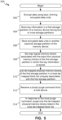
- LBAs may be de-mapped from physical memory blocks of a storage partition of the memory device.
- This storage partition may be, for example, a special partition as described above with regard to FIG. 2 (e.g., the first partition 102A).
- de-mapped physical memory blocks of that storage partition may be listed in a local de-mapped block list uniquely associated with that storage partition.
- a local purge command may be received from a host device.
- only the de-mapped physical memory blocks listed in the local de-mapped block list may be purged.
- de-mapped physical memory blocks listed in any other de-mapped block list such as a global de-mapped block list
- the method 300 may be provided in addition to a method (not shown) by which de-mapped physical memory blocks listed in a global de-mapped block list, covering all partitions of the memory device, may be purged. It should be understood that although blocks 302-308 are described above in an exemplary order conducive to guiding the reader through an example of the method 300, the actions described above in association with blocks 302-308 may occur in any order that produces the same or similar results.
- the local purge feature may be used to, in effect, purge encrypted data stored in the second through Nth partitions 102B-102N.
- This feature is sometimes referred to as a cryptographic purge.
- a local purge operation may only actually purge data blocks 104 in the first partition 102A, in an embodiment in which the data blocks 104 in the first partition 102A are used to store key information associated with encrypted data stored in data blocks 104 in any of the second through Nth partitions 102B-102N, purging the key information in effect purges data encrypted in association with the key information.
- encryption of data in some exemplary data blocks 104 in the second through Nth partitions 102B-102N by key information in other exemplary data blocks 104 in the first partition 102A is conceptually indicated by broken-line arrows.
- the encryption keys may be stored in an encrypted form by a technique sometimes referred to as key wrapping.
- a key wrapping scheme 400 may involve several types of keys and several operations or functions.
- the key wrapping scheme 400 may be provided in the host system 204 ( FIG. 2 ).
- a key derivation function 402 may operate upon inputs comprising a seed 403 (i.e., a randomly generated number), a unique hardware key 404 and user credentials (or context) to produce a key wrapping key 406.
- a key generator 408 may produce a (random) storage encryption key 410.
- a key wrapping function 412 may operate upon inputs comprising the key wrapping key 406 and the storage encryption key 410 to produce a wrapped storage encryption key 414.
- the wrapped storage encryption key 414 and the seed 403 may be stored in a block 104 in a form sometimes referred to as a binary large object or "blob."
- the above-referenced "key information" may include the wrapped storage encryption key 414, the seed 403 to that key 414, or other information that may enable recovery of the encrypted data.
- all of the data stored in blocks 104 in the partitions 102B-102N may be encrypted by keys (in the form of key blobs, for example) stored in blocks 104 in the first partition 102A.
- purging the first partition 102A, containing the key information in effect (or from a cryptographic perspective) purges all of the partitions 102A-102N because the data cannot be retrieved without the key information.
- purging only the first partition 102A may be substantially faster than purging all of the partitions 102A-102N.
- a method 500 for purging data from a memory device having two or more storage partitions is illustrated in flow diagram form.
- data may be encrypted using corresponding keys to form encrypted data units.
- the key information may be stored in a first storage partition.
- This first storage partition may be, for example, a special partition as described above with regard to FIG. 2 (e.g., the first partition 102A), in contrast with some other (second, third, etc.) storage partition of the memory device.
- the encrypted data units may be stored in another (second) storage partition of the memory device.
- logical memory blocks associated with the keys may be de-mapped from physical memory blocks in which the key information was stored (block 504).
- de-mapped physical memory blocks of the first storage partition may be listed in a local de-mapped block list uniquely associated with the first storage partition.
- a local purge command may be received from a host device.
- only the de-mapped physical memory blocks listed in the local de-mapped block list (and thus including de-mapped physical memory blocks in which the key information was stored) may be purged.
- de-mapped physical memory blocks listed in any other de-mapped block list may not be purged in response to the local purge command.
- the method 500 may be provided in addition to a method (not shown) by which de-mapped physical memory blocks listed in a global de-mapped block list covering all partitions of the memory device may be purged. It should be understood that although blocks 502-514 are described above in an exemplary order conducive to guiding the reader through an example of the method 500, the actions described above in association with blocks 502-514 may occur in any order that produces the same or similar results.
- a key hierarchy 600 illustrates that the above-referenced keys may be of any type.
- the above-referenced keys may be any of: a user key 602 (e.g., a first user key 602A associated with a first user, a second user key 602B associated with a second user, etc.); an application-specific key 604 (e.g., a first application-specific key 604A associated with a first application program, a second application-specific key 604B associated with a second application program, etc.); or a folder key 606 (e.g., a first folder key 606A associated with a first folder of the first application program, a second folder key 606B associated with a second folder of the first application program, etc.).
- a user key 602 e.g., a first user key 602A associated with a first user, a second user key 602B associated with a second user, etc.
- an application-specific key 604 e.g., a first application-
- the key hierarchy 600 may be maintained in the above-described special partition of the memory device by a key management system (not shown) of the host system 204 ( FIG. 2 ).
- Each user key 602 may be unique to a user of the application programs on the host system 204.
- the key management system may use a user key 602 to wrap an application-specific key 604, and may use an application-specific key 604 to wrap a folder key 606.
- an application program deletes a folder protected by a folder key 606
- the key management system may generate a new application-specific key 604 and re-wrap all the associated folder keys 606.
- the key management system may use that user's user key 602 to wrap the application-specific keys 604.
- the key management system may remove that user's user key 602 from the special partition in which keys are stored. Removing a key from the special partition may comprise de-mapping the block containing the key.
- the key management system may purge the special partition (thus purging all de-mapped keys) in the manner described above.
- the key management system may purge the special partition at any time, such as, for example, hourly, daily, etc., or when a block containing a key is de-mapped.
- a purge count feature may be included in some embodiments, such as an embodiment in which a local free block list is utilized instead of the global free block list.
- the key management system (not shown) of the host system 204 may determine how frequently to purge the special partition based on the number of lifetime erase cycles of which the flash storage medium 208 ( FIG. 2 ) is capable and the total number of purge operations that the special partition has undergone.
- the flash memory device 202 may include a purge counter 218.
- the controller 206 may increment the purge counter 218 each time the controller 206 performs a purge operation on the special partition.
- the controller 206 may not only perform the purge operation but also return the purge count or value in the purge counter 218 to the host system 204. Based on that purge count (or the purge count in combination with other information, such as the number of lifetime erase cycles of which the flash memory device is capable) the key management system may determine when to initiate the next purge operation.
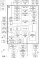
- exemplary embodiments of systems and methods for purging data from a memory device may be provided in a portable computing device (“PCD") 700.
- PCD portable computing device
- data buses or other data communication interconnects are not shown in FIG. 7 .
- Some exemplary interconnections, some of which may represent communication via such buses or interconnects, are described for context. Nevertheless, it should be understood that, more generally, various elements described below may communicate with each other via one or more buses or system interconnects.
- the PCD 700 may include an SoC 702.
- the SoC 702 may include a CPU 704, a GPU 706, a DSP 707, an analog signal processor 708, or other processors.
- the CPU 704 may include multiple cores, such as a first core 704A, a second core 704B, etc., through an Nth core 704N.
- a display controller 710 and a touch-screen controller 712 may be coupled to the CPU 704.
- a touchscreen display 714 external to the SoC 702 may be coupled to the display controller 710 and the touch-screen controller 712.
- the PCD 700 may further include a video decoder 716 coupled to the CPU 704.
- a video amplifier 718 may be coupled to the video decoder 716 and the touchscreen display 714.
- a video port 720 may be coupled to the video amplifier 718.
- a universal serial bus (“USB”) controller 722 may also be coupled to CPU 704, and a USB port 724 may be coupled to the USB controller 722.
- a subscriber identity module (“SIM”) card 726 may also be coupled to the CPU 704.
- One or more memories may be coupled to the CPU 704.
- the one or more memories may include both volatile and non-volatile memories. Examples of volatile memories include static random access memory (“SRAM”) 728 and dynamic RAMs (“DRAM”s) 730 and 731. Such memories may be external to the SoC 702, such as the DRAM 730, or internal to the SoC 702, such as the DRAM 731.
- a DRAM controller 732 coupled to the CPU 704 may control the writing of data to, and reading of data from, the DRAMs 730 and 731. In other embodiments, such a DRAM controller may be included within a processor, such as the CPU 704.
- the PCD 700 may include a flash memory device 733, such as a chip that is coupled to the SoC 702.
- the flash memory device 733 may be coupled to the CPU 704 via, for example, an input/output ("I/O") interface 735.
- the I/O interface 735 may comprise a bus, such as, for example, a peripheral component interconnect express ("PCIe") bus, or any other type of interconnection with the CPU 704.
- the flash memory device 733 may be an example of the flash memory device 202 described above with regard to FIG. 2 . Although in this embodiment the flash memory device 202 includes the controller 206 ( FIG. 2 ), in other embodiments such a controller may be included in the SoC.
- the CPU 704 and related components may be configured to provide the host system functions described above.
- a modem or RF transceiver 754 may be coupled to the analog signal processor 708 and the CPU 704.
- An RF switch 756 may be coupled to the RF transceiver 754 and an RF antenna 758.
- a keypad 760, a mono headset with a microphone 762, and a vibrator device 764 may be coupled to the analog signal processor 708.
- the SoC 702 may have one or more internal or on-chip thermal sensors 770A and may be coupled to one or more external or off-chip thermal sensors 770B.
- An analog-to-digital converter (“ADC") controller 772 may convert voltage drops produced by the thermal sensors 770A and 770B to digital signals.
- a power supply 774 and a power management integrated circuit (“PMIC”) 776 may supply power to the SoC 702.
- Firmware or software may be stored in any of the above-described memories, such as DRAM 730 or 731, SRAM 728, etc., or may be stored in a local memory directly accessible by the processor hardware on which the software or firmware executes. Execution of such firmware or software may control aspects of any of the above-described methods or configure aspects any of the above-described systems. Any such memory or other non-transitory storage medium having firmware or software stored therein in computer-readable form for execution by processor hardware may be an example of a "computer-readable medium,” as the term is understood in the patent lexicon.
- the above-described local Purge command may be included in a set of commands covered by a flash memory standard, such as, for example a UFS standard.
- the local Purge command may be included in the (e.g., UFS) command set in addition to the above-described global Purge command.
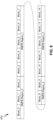
- An example 800 of a local Purge command is shown in conceptual form in FIG. 8 .
- the special or local partition may be the RPMB.
- the local Purge command may take arguments that specify a region within the local partition (i.e., a subset of the RPMB blocks).
- the host could set the value of an argument to identify any of: a first region (RMPB Region _0) that spans blocks 0 through 2 of the RPMB; a second region (RMPB Region_1) that spans blocks 3 through 7 of the RPMB; a third region (RMPB Region_2) that spans blocks 8 through 9 of the RPMB; a fourth region (RMPB Region_3) that spans blocks 10 through 14 of the RPMB; etc.
- the regions shown in FIG. 8 are intended only as examples and, using the local Purge command arguments, a host could define any group of blocks as such a region.
- a flash memory device In response to a local Purge command received from a host, a flash memory device, such as a UFS device, may purge only those blocks identified by the values of the arguments in the local Purge command. In this manner, a host may purge all or only a subset of the blocks in the local partition (e.g., RPMB).
- RPMB a subset of the blocks in the local partition
Landscapes
- Engineering & Computer Science (AREA)
- Theoretical Computer Science (AREA)
- Physics & Mathematics (AREA)
- General Engineering & Computer Science (AREA)
- General Physics & Mathematics (AREA)
- Human Computer Interaction (AREA)
- Computer Security & Cryptography (AREA)
- Information Retrieval, Db Structures And Fs Structures Therefor (AREA)
- Memory System (AREA)
- Techniques For Improving Reliability Of Storages (AREA)
Description
- The invention relates to flash memories.
- A computing device may include multiple subsystems that communicate with one another via buses or other interconnects. Such a computing device may be, for example, a portable computing device ("PCD"), such as a laptop or palmtop computer, a cellular telephone or smartphone, portable digital assistant, portable game console, etc. The communicating subsystems may be included within the same integrated circuit chip or in different chips. A "system-on-a-chip" or "SoC" is an example of one such chip that integrates numerous components to provide system-level functionality.
- For example, an SoC may include one or more types of processors, such as central processing units ("CPU"s), graphics processing units ("GPU"s), digital signal processors ("DSP"s), and neural processing units ("NPU"s). An SoC may include other subsystems, such as a transceiver or "modem" that provides wireless connectivity, a main or system memory, one or more cache memories, etc. Some subsystems may include processing engines that may perform memory transactions with a memory. The system memory in PCDs and other computing devices commonly comprises dynamic random access memory ("DRAM"). In addition to DRAM, or alternatively to DRAM, a computing device may include non-volatile memory, such as flash memory.
- A computing device may "delete" data, such as when a user requests deletion of a file, when an application program deletes temporary data that it no longer requires, etc. Nevertheless, deleting data in this manner does not physically remove the data from storage in the memory. Rather, deleting data in such a manner only causes the memory controller to de-map logical addresses by which the host (e.g., a processing engine) identifies the data from physical addresses identifying locations at which the data is physically stored in the memory. Such de-mapping, in conjunction with a process known as "garbage collection," enables the physical locations to be re-used. Nevertheless, it may be possible for a hacker or other party to retrieve deleted or otherwise de-mapped data (e.g., during a window after deletion but before garbage collection).
- As confidential or otherwise sensitive data is commonly stored in the memories of PCDs and other computing devices, it is desirable to prevent retrieval of de-mapped data. "Purging" is a term that is commonly used to refer to physically eliminating data from a memory in a way that prevents the data from being retrieved. Purging flash memory is challenging because features known as write-leveling and garbage collection commonly result in multiple copies of data being distributed about the various physical "blocks." Flash memory may be purged by a host sending a purge command to a flash memory device. In response to the purge command, the flash memory device may purge all de-mapped blocks in the flash memory device. Flash memory also may be purged by performing a so-called "factory reset," in which all blocks of the memory are de-mapped, followed by a purge operation on the de-mapped blocks. Purging flash memory in this manner may take a substantial amount of time, which may inconvenience the user or otherwise be undesirable.
- Attention is drawn to
US 2012/278529 A1 describing method and apparatus for the nondestructive, selective purging of data from a non-volatile memory. Multiple copies of a selected set of confidential user data having a common logical address are stored to a confidential data portion of a non-volatile memory so that each copy is in a different location within the confidential data portion. A nondestructive purge of all said copies from the confidential data portion is carried out responsive to an externally supplied selective purge command so that all said copies are erased and other, non-purged confidential user data remain stored in the confidential data portion. - The invention is defined by the appended independent claims. Further embodiments are defined by the appended dependent claims.
- Systems, methods, computer-readable media, and other examples are disclosed for purging data from a memory device.
- In the Figures, like reference numerals refer to like parts throughout the various views unless otherwise indicated. For reference numerals with letter character designations such as "102A" or "102B", the letter character designations may differentiate two like parts or elements present in the same Figure. Letter character designations for reference numerals may be omitted when it is intended that a reference numeral to encompass all parts having the same reference numeral in all Figures.
-
FIG. 1 is a memory map for a memory device, in accordance with exemplary embodiments. -
FIG. 2 is a block diagram of a system for purging data from a memory device, in accordance with exemplary embodiments. -
FIG. 3 is a flow diagram of a method for purging data from a memory device, in accordance with exemplary embodiments. -
FIG. 4 is a key wrapping scheme diagram, in accordance with exemplary embodiments. -
FIG. 5 is a flow diagram of another method for purging data from a memory device, in accordance with exemplary embodiments. -
FIG. 6 is a key hierarchy diagram, in accordance with exemplary embodiments. -
FIG. 7 is a block diagram of a portable computing device, in accordance with exemplary embodiments. -
FIG. 8 is a conceptual illustration of a local purge command, in accordance with exemplary embodiments. - As illustrated in
FIG. 1 , amemory map 100 represents storage space in a memory device (not shown). Thememory map 100 may includepartitions 102, such as afirst partition 102A, asecond partition 102B, etc., through anNth partition 102N. The terms "first," "second," etc., are used herein only as an aid for referencing distinct elements and should not be construed as implying any location, order, sequence, etc. There may be any number (N) ofpartitions 102. Thememory map 100 is depicted in a conceptual manner inFIG. 1 and is not intended to indicate actual memory addresses. - Data may be stored in the
partitions 102 in locations that may be referred to herein asblocks 104. That is, eachblock 104 has a physical block address ("PBA") that may be used to write data to (i.e., physically store data in) or read data from (i.e., physically retrieve data from) that block 104. The illustratedblocks 104 are intended only as examples, and there may be any number ofblocks 104 in any of thepartitions 102. - The
memory map 100 may also include regions relating to management of theblocks 104 in the first throughNth partitions 102A-102N: a global usedblock list 106, a global garbage block list 108, and a globalfree block list 110. Block "management" refers to processes by whichblocks 104 may be made available for data storage, such as when data is stored in ablock 104, after data is deleted, etc. Block management also involves moving information identifying theblocks 104, such as block addresses, from one of the lists 106-110 to another of the lists 106-110. For reasons described below, used blocks may also be referred to as mapped blocks, and garbage blocks may also be referred to as de-mapped blocks. - In the exemplary embodiment illustrated in
FIGs. 1-2 , thememory map 100 may further include regions relating to management of theblocks 104 in thefirst partition 102A only: a local usedblock list 112 and a localgarbage block list 114. A localfree block list 116 may also be included. That is, while the global usedblock list 106, global garbage block list 108, and globalfree block list 110 are associated with all of thepartitions 102A-102N in the illustrated embodiment, the local usedblock list 112, localgarbage block list 114, and localfree block list 116 are associated with only thefirst partition 102A in the illustrated embodiment. Nevertheless, in other embodiments such a memory map may omit the localfree block list 116 and instead use the globalfree block list 110. A potential issue is that in embodiments utilizing the localfree block list 116, excessive use of the local purge function described below could prematurely wear the memory locations, whereas wear leveling may mitigate such wear in embodiments omitting the localfree block list 116 and utilizing only the globalfree block list 110. - As illustrated in
FIG. 2 , in a system 200 aflash memory device 202 is coupled to ahost system 204. Thehost system 204 may be, for example, a computing device or portion thereof, such as a processor subsystem, processing engine, etc. - In the illustrated embodiment the
flash memory device 202 has storage block management features and thus may be of a type commonly referred to as a "managed" memory device. Examples of managed memory devices include Universal Flash Storage ("UFS"), Embedded Multi-media Card ("eMMC"), Non-volatile Memory Express ("NVMe"), etc. Thus, in other embodiments of the system the memory device may be of any of the foregoing or other non-volatile, managed memory types. Theflash memory device 202 may include acontroller 206. Thecontroller 206 may provide functions associated with a memory controller of a solid-state storage (e.g., flash memory) drive, including, for example, storage block management. Thecontroller 206 may be configured to perform conventional functions associated with a memory controller of a flash memory drive, such as aspects relating to writing and reading data, as well as functions described below relating to purging de-mapped blocks. Conventional aspects of theflash memory device 202 that are well understood by one of ordinary skill in the art are not described in detail herein. - The
flash memory device 202 may also include a flashdata storage medium 208. As understood by one of ordinary skill in the art, the flashdata storage medium 208 may comprise (not shown for purposes of clarity) one or more dies, each die having one or more planes, each plane having some number (commonly on the order of thousands but potentially any number) of blocks, and each block having some number (commonly on the order of dozens but potentially any number) of pages. - Data may be stored in the
flash memory device 202 at the initiation of thehost system 204, i.e., in response to a write request (command) issued by thehost system 204. The write command may include one or more logical block addresses ("LBA"s) identifying locations in the host or "logical" address space at which thehost system 204 requests the data be stored. When data is to be stored in theflash memory device 202, thecontroller 206 generates a mapping between each LBA and one or more PBAs. This mapping (of a block 104) may be stored in a mapping table 210 associated with a Flash Translation Layer ("FTL") 212 with which thecontroller 206 is configured (e.g., by software or firmware). Ablock 104 that has been mapped may also be referred to as a "used"block 104, i.e., theblock 104 is in use. Thecontroller 206 may add the LBA of each mappedblock 104 to the global used block list 106 (FIG. 1 ). - The
flash memory device 202 may also have ahost interface 214 and a flashphysical interface 216, which may comprise portions of thecontroller 206. Under control of thecontroller 206, data that is the subject of the write request may be stored in thestorage medium 208 at locations corresponding to the PBAs of the mapping. Details of the manner by which data may be conveyed from thehost system 204 to thestorage medium 208 and stored therein under control of the controller 206 (e.g., via thehost interface 214 and flash physical interface 216) are well understood by one of ordinary skill in the art and therefore not described herein. - The
host system 204 may address the data that is the subject of read and write commands using LBAs. Although not shown for purposes of clarity, the portion of thehost system 204 that allocates and de-allocates LBAs based on the operation of application programs or other software in operation is commonly referred to as a file system. The file system may be part of the operating system of thehost system 204. - Commonly, the
flash storage medium 208 is not over-writeable. Rather, data can only be stored in a block 104 (FIG. 1 ) that has been erased. An erased block may also be referred to as being in a "free" state.Blocks 104 that have been erased may be listed in the global free list 110 (FIG. 1 ). In embodiments in which the flash storage medium is over-writable, blocks may be listed in the globalfree list 110 without first erasing them. In generating the above-described mapping in response to a write command, thecontroller 206 may select a PBA from the globalfree list 110. - As understood by one of ordinary skill in the art, physical locations in the
storage medium 208 have a limited lifespan. That is, after some number of accesses (e.g., Erase and Program flash memory commands), each location will be worn to an extent that it may no longer function properly. To mitigate this "wear" effect, a flash memory controller may run a process known as wear leveling. In accordance with wear leveling, thecontroller 206 may attempt to distribute data evenly over allblocks 104 to avoid wearing someblocks 104 more than others. Wear-leveling, like the above-described mapping, is another function of theFTL 212. - Data stored in the
flash memory device 202 may be deleted from the perspective of thehost system 204. To delete data in this manner, thehost system 204 may issue a Write or Erase command to theflash memory device 202. The Write or Erase command may include one or more LBAs identifying locations from which thehost system 204 requests the data to be deleted. In response to a Write or Erase command, thecontroller 206 may remove the mappings between one or more PBAs and LBAs from the mapping table 210. For clarity, a command issued by thehost system 204 that causes thecontroller 206 to remove such mappings (e.g., a Write or Erase command) may be referred to in this disclosure as a "de-map" command. Thecontroller 206 may also move the PBA of each de-mapped block 104 (FIG. 1 ) from the global usedblock list 106 to the global garbage block list 108. - In a process commonly referred to as garbage collection, the
controller 206 may sometimes move data (pages) inblocks 104 listed in the global usedblock list 106 toother blocks 104 and update the mapping table 210 accordingly. The goal of such movement of data is to remove some of theblocks 104 from use, so that thoseblocks 104 no longer in use can be erased and then re-used to store new data. When ablock 104 no longer contains data that is in use, thecontroller 206 may move the PBA of thatblock 104 from the global usedblock list 106 to the global garbage block list 108. Thecontroller 206 may erase theblocks 104 listed in the global garbage block list 108 and move the PBAs of the erasedblocks 104 to the globalfree block list 110. Garbage collection, like the above-described mapping, is another function of theFTL 212. Thecontroller 206 may perform garbage collection in the background, i.e., at times during which thehost system 204 is not interacting with theflash memory device 202. - For security reasons, it may be desirable to prevent retrieval of de-mapped data (i.e., data that is invalid or no longer in use) from the
storage medium 208. Although the above-described de-mapping prevents thehost system 204 from accessing the data (addressed by LBAs), such de-mapping does not affect the physical state of the data in thestorage medium 208. Absent the purge-related features described below, it may be possible for a hacker or other party to retrieve de-mapped data from thestorage medium 208 using, for example, a software tool (i.e., software other than the file system of the host system 204). - Terms such as "sanitizing," "wiping," etc. commonly refer to eliminating physical manifestations of de-mapped data from a memory to prevent the data from being retrieved. Performing such operations on flash memory may be challenging because, among other reasons, operation of the above-described wear leveling, garbage collection, etc., features may result in multiple copies of the same data distributed about the
storage medium 208. - Managed flash devices, such as UFS devices, may implement a Purge command, which may be referred to herein as a global Purge command to distinguish it from a local purge command that is described below. In response to a global Purge command issued by the
host system 204, thecontroller 206 may erase allde-mapped blocks 104. Managed flash devices also may implement a Format Unit command. In response to a Format Unit command issued by thehost system 204, thecontroller 206 may erase all de-mapped blocks 104 (e.g., in response to an Erase command) and then write various data values, such as all zeroes, all ones, random numbers, etc., to the erasedblocks 104 to obscure any remaining physical manifestations of the originally stored data. Thecontroller 206 may move the PBAs of purgedblocks 104 from the global garbage block list 108 to the globalfree block list 110. - When the global garbage block list 108 contains many
de-mapped blocks 104, purging them in the manner described above in response to a global Purge command or a Format Unit command may be time-consuming. A global purge operation as described above may take, for example, an amount of time on the order of hours. To provide a faster purge operation than the global purge operation, thedevice 202 may be provided with the following local purge feature in addition to, or alternatively to, the global purge feature described above. - At least one of the
partitions 102, which may be referred to as a "special" or "local" partition, may have one or more characteristics that are different fromother partitions 102. In the illustrated embodiment, thefirst partition 102A may be the special or local partition, as depicted inFIG. 1 by a border in bold line. In the illustrated embodiment, the special characteristics of thefirst partition 102A include the local usedblock list 112, the localgarbage block list 114, and the localfree block list 116. As noted above, in some embodiments the localfree block list 116 may be omitted. In the illustrated embodiment,partitions 102 other than thefirst partition 102A do not include such a local used block list, local garbage block list or local free block list. - The special or local partition, such as the
first partition 102A in the illustrated embodiment, may be, for example, a Replay-Protected Memory Block ("RPMB"). An RPMB is a type of authenticated-access partition. An entity (e.g., host system 204) may only be granted access to an authenticated-access partition, such as an RPMB, when authentication of the entity is successful. Nevertheless, in other embodiments the special partition may be any partition (sometimes also referred to as a Logical Unit) of the storage medium. - To provide the local purge feature, the
controller 206 may be configured (e.g., by software or firmware) to respond to a local purge command received from thehost system 204 in a manner similar to the above-described manner in which thecontroller 206 responds to a global purge command. However, in an exemplary embodiment, unlike the global purge operation, which purges all blocks 104 (FIG. 1 ) listed in the global garbage block list 108, the local purge operation purges only theblocks 104 listed in the localgarbage block list 114. Thus, in this exemplary embodiment, unlike the global purge operation, which may purgeblocks 104 in any of the first throughNth partitions 102A-102N, the local purge operation may purgeblocks 104 in only thefirst partition 102A and not purge any blocks in any of the second throughNth partitions 102B-102N. The local purge operation may comprise thecontroller 206 erasing allblocks 104 listed in the localgarbage block list 114. The local purge operation may also comprise the controller writing various data values, such as all zeroes, all ones, random numbers, etc., to those erasedblocks 104 to obscure any remaining physical manifestations of the originally stored data. Thecontroller 206 may move the PBAs of purgedblocks 104 from the localgarbage block list 114 to the global free block list 110 (or, in some embodiments, to the local free block list 116). The local purge operation may be completed within a substantially shorter amount of time than a global purge operation because the local purge operation is confined to the special partition (e.g., thefirst partition 102A in this exemplary embodiment). - The
controller 206 may be configured to perform garbage collection in thefirst partition 102A in a manner similar to the above-described manner in which thecontroller 206 may perform garbage collection inpartitions 102 in general. That is, thecontroller 206 may sometimes move data (pages) inblocks 104 listed in the local usedblock list 112 toother blocks 104 in thefirst partition 102A and update the mapping table 210 accordingly, with the goal of removing some of theblocks 104 in thefirst partition 102A from use. When ablock 104 listed in the local usedblock list 112 no longer contains data that is in use, thecontroller 206 may move the PBA of thatblock 104 from the local usedblock list 112 to the localgarbage block list 114. Thecontroller 206 may erase theblocks 104 listed in the localgarbage block list 114 and move the PBAs of those erasedblocks 104 to the global free block list 110 (or, in some embodiments, to the local free block list 116). - Note that while both garbage collection and purge operations involve erasing
blocks 104, garbage collection commonly results in only a fraction of thede-mapped blocks 104 being erased at a time. In contrast, a purge operation may erase all de-mapped blocks 104: a global purge operation may erase allde-mapped blocks 104 listed in the global garbage block list 108, and a local purge operation may erase onlyde-mapped blocks 104 listed in the localgarbage block list 114. - Write operations directed to the
first partition 102A may be performed in a manner similar to the manner described above with regard to any of thepartitions 102, except that block management operations associated with thefirst partition 102A may use the local usedblock list 112 and localgarbage block list 114 instead of the global usedblock list 106 and global garbage block list 108, respectively. In some embodiments, the localfree block list 116 may be used instead of, or in addition to, the globalfree block list 110. Accordingly, in response to receiving a write request (command) from thehost system 204, thecontroller 206 may select one ormore blocks 104 listed in the global free block list 110 (as identified by PBA), generate a mapping between each LBA and the one or more PBAs, store the one or more mappings in the mapping table 210, store the data that is the subject of the write request in thestorage medium 208, and add the PBA of each mappedblock 104 to the local usedblock list 112. As noted above, in the exemplary embodiment a prerequisite or condition of completing a write operation or other access in thefirst partition 102A is successful authentication of thehost system 204. Nevertheless, in other embodiments, the special partition may not be an authenticated-access block, and authentication thus may not be required for a host system to access the special partition in such other embodiments. - In
FIG. 3 , amethod 300 for purging data from a memory device having two or more storage partitions is illustrated in flow diagram form. As indicated byblock 302, LBAs may be de-mapped from physical memory blocks of a storage partition of the memory device. This storage partition may be, for example, a special partition as described above with regard toFIG. 2 (e.g., thefirst partition 102A). As indicated byblock 304, de-mapped physical memory blocks of that storage partition may be listed in a local de-mapped block list uniquely associated with that storage partition. As indicated byblock 306, a local purge command may be received from a host device. As indicated byblock 308, in response to the local purge command, only the de-mapped physical memory blocks listed in the local de-mapped block list may be purged. That is, de-mapped physical memory blocks listed in any other de-mapped block list, such as a global de-mapped block list, may not be purged in response to this local type of purge command. In some embodiments, themethod 300 may be provided in addition to a method (not shown) by which de-mapped physical memory blocks listed in a global de-mapped block list, covering all partitions of the memory device, may be purged. It should be understood that although blocks 302-308 are described above in an exemplary order conducive to guiding the reader through an example of themethod 300, the actions described above in association with blocks 302-308 may occur in any order that produces the same or similar results. - Conveniently, the local purge feature may be used to, in effect, purge encrypted data stored in the second through
Nth partitions 102B-102N. This feature is sometimes referred to as a cryptographic purge. Although a local purge operation may only actually purge data blocks 104 in thefirst partition 102A, in an embodiment in which the data blocks 104 in thefirst partition 102A are used to store key information associated with encrypted data stored in data blocks 104 in any of the second throughNth partitions 102B-102N, purging the key information in effect purges data encrypted in association with the key information. InFIG. 1 , encryption of data in some exemplary data blocks 104 in the second throughNth partitions 102B-102N by key information in other exemplary data blocks 104 in thefirst partition 102A is conceptually indicated by broken-line arrows. The encryption keys may be stored in an encrypted form by a technique sometimes referred to as key wrapping. - As illustrated in
FIG. 4 , akey wrapping scheme 400 may involve several types of keys and several operations or functions. Thekey wrapping scheme 400 may be provided in the host system 204 (FIG. 2 ). Akey derivation function 402 may operate upon inputs comprising a seed 403 (i.e., a randomly generated number), aunique hardware key 404 and user credentials (or context) to produce akey wrapping key 406. Akey generator 408 may produce a (random)storage encryption key 410. Akey wrapping function 412 may operate upon inputs comprising thekey wrapping key 406 and thestorage encryption key 410 to produce a wrappedstorage encryption key 414. The wrappedstorage encryption key 414 and theseed 403 may be stored in ablock 104 in a form sometimes referred to as a binary large object or "blob." The above-referenced "key information" may include the wrappedstorage encryption key 414, theseed 403 to that key 414, or other information that may enable recovery of the encrypted data. In an exemplary embodiment, all of the data stored inblocks 104 in thepartitions 102B-102N may be encrypted by keys (in the form of key blobs, for example) stored inblocks 104 in thefirst partition 102A. In such an embodiment, purging thefirst partition 102A, containing the key information, in effect (or from a cryptographic perspective) purges all of thepartitions 102A-102N because the data cannot be retrieved without the key information. As noted above, purging only thefirst partition 102A may be substantially faster than purging all of thepartitions 102A-102N. - In
FIG. 5 , amethod 500 for purging data from a memory device having two or more storage partitions is illustrated in flow diagram form. As indicated byblock 502, data may be encrypted using corresponding keys to form encrypted data units. As indicated byblock 504, the key information may be stored in a first storage partition. This first storage partition may be, for example, a special partition as described above with regard toFIG. 2 (e.g., thefirst partition 102A), in contrast with some other (second, third, etc.) storage partition of the memory device. As indicated byblock 506, the encrypted data units may be stored in another (second) storage partition of the memory device. - As indicated by
block 508, logical memory blocks associated with the keys may be de-mapped from physical memory blocks in which the key information was stored (block 504). As indicated byblock 510, de-mapped physical memory blocks of the first storage partition may be listed in a local de-mapped block list uniquely associated with the first storage partition. As indicated byblock 512, a local purge command may be received from a host device. As indicated byblock 514, in response to the local purge command, only the de-mapped physical memory blocks listed in the local de-mapped block list (and thus including de-mapped physical memory blocks in which the key information was stored) may be purged. That is, de-mapped physical memory blocks listed in any other de-mapped block list, such as a global de-mapped block list, may not be purged in response to the local purge command. In some embodiments, themethod 500 may be provided in addition to a method (not shown) by which de-mapped physical memory blocks listed in a global de-mapped block list covering all partitions of the memory device may be purged. It should be understood that although blocks 502-514 are described above in an exemplary order conducive to guiding the reader through an example of themethod 500, the actions described above in association with blocks 502-514 may occur in any order that produces the same or similar results. - In
FIG. 6 , akey hierarchy 600 illustrates that the above-referenced keys may be of any type. For example, the above-referenced keys may be any of: a user key 602 (e.g., afirst user key 602A associated with a first user, asecond user key 602B associated with a second user, etc.); an application-specific key 604 (e.g., a first application-specific key 604A associated with a first application program, a second application-specific key 604B associated with a second application program, etc.); or a folder key 606 (e.g., afirst folder key 606A associated with a first folder of the first application program, a second folder key 606B associated with a second folder of the first application program, etc.). - The
key hierarchy 600 may be maintained in the above-described special partition of the memory device by a key management system (not shown) of the host system 204 (FIG. 2 ). Eachuser key 602 may be unique to a user of the application programs on thehost system 204. The key management system may use auser key 602 to wrap an application-specific key 604, and may use an application-specific key 604 to wrap afolder key 606. When an application program deletes a folder protected by afolder key 606, the key management system may generate a new application-specific key 604 and re-wrap all the associatedfolder keys 606. When a different user requires access to the application programs, the key management system may use that user'suser key 602 to wrap the application-specific keys 604. When a user no longer requires access to the application programs, the key management system may remove that user'suser key 602 from the special partition in which keys are stored. Removing a key from the special partition may comprise de-mapping the block containing the key. The key management system may purge the special partition (thus purging all de-mapped keys) in the manner described above. The key management system may purge the special partition at any time, such as, for example, hourly, daily, etc., or when a block containing a key is de-mapped. - A purge count feature may be included in some embodiments, such as an embodiment in which a local free block list is utilized instead of the global free block list. Referring again to
FIG. 2 , the key management system (not shown) of thehost system 204 may determine how frequently to purge the special partition based on the number of lifetime erase cycles of which the flash storage medium 208 (FIG. 2 ) is capable and the total number of purge operations that the special partition has undergone. Theflash memory device 202 may include apurge counter 218. Thecontroller 206 may increment thepurge counter 218 each time thecontroller 206 performs a purge operation on the special partition. In response to a local purge command received from thehost system 204, thecontroller 206 may not only perform the purge operation but also return the purge count or value in thepurge counter 218 to thehost system 204. Based on that purge count (or the purge count in combination with other information, such as the number of lifetime erase cycles of which the flash memory device is capable) the key management system may determine when to initiate the next purge operation. - As illustrated in
FIG. 7 , exemplary embodiments of systems and methods for purging data from a memory device may be provided in a portable computing device ("PCD") 700. For purposes of clarity, data buses or other data communication interconnects are not shown inFIG. 7 . Some exemplary interconnections, some of which may represent communication via such buses or interconnects, are described for context. Nevertheless, it should be understood that, more generally, various elements described below may communicate with each other via one or more buses or system interconnects. - The
PCD 700 may include anSoC 702. TheSoC 702 may include aCPU 704, aGPU 706, aDSP 707, ananalog signal processor 708, or other processors. TheCPU 704 may include multiple cores, such as afirst core 704A, asecond core 704B, etc., through anNth core 704N. - A
display controller 710 and a touch-screen controller 712 may be coupled to theCPU 704. Atouchscreen display 714 external to theSoC 702 may be coupled to thedisplay controller 710 and the touch-screen controller 712. ThePCD 700 may further include avideo decoder 716 coupled to theCPU 704. Avideo amplifier 718 may be coupled to thevideo decoder 716 and thetouchscreen display 714. Avideo port 720 may be coupled to thevideo amplifier 718. A universal serial bus ("USB")controller 722 may also be coupled toCPU 704, and aUSB port 724 may be coupled to theUSB controller 722. A subscriber identity module ("SIM")card 726 may also be coupled to theCPU 704. - One or more memories may be coupled to the
CPU 704. The one or more memories may include both volatile and non-volatile memories. Examples of volatile memories include static random access memory ("SRAM") 728 and dynamic RAMs ("DRAM"s) 730 and 731. Such memories may be external to theSoC 702, such as theDRAM 730, or internal to theSoC 702, such as theDRAM 731. ADRAM controller 732 coupled to theCPU 704 may control the writing of data to, and reading of data from, theDRAMs CPU 704. - The
PCD 700 may include aflash memory device 733, such as a chip that is coupled to theSoC 702. Theflash memory device 733 may be coupled to theCPU 704 via, for example, an input/output ("I/O")interface 735. The I/O interface 735 may comprise a bus, such as, for example, a peripheral component interconnect express ("PCIe") bus, or any other type of interconnection with theCPU 704. Theflash memory device 733 may be an example of theflash memory device 202 described above with regard toFIG. 2 . Although in this embodiment theflash memory device 202 includes the controller 206 (FIG. 2 ), in other embodiments such a controller may be included in the SoC. TheCPU 704 and related components may be configured to provide the host system functions described above. - A
stereo audio CODEC 734 may be coupled to theanalog signal processor 708. Further, anaudio amplifier 736 may be coupled to thestereo audio CODEC 734. First and secondstereo speakers audio amplifier 736. In addition, amicrophone amplifier 742 may be coupled to thestereo audio CODEC 734, and amicrophone 744 may be coupled to themicrophone amplifier 742. A frequency modulation ("FM")radio tuner 746 may be coupled to thestereo audio CODEC 734. AnFM antenna 748 may be coupled to theFM radio tuner 746. Further,stereo headphones 750 may be coupled to thestereo audio CODEC 734. Other devices that may be coupled to theCPU 704 include one or more digital (e.g., CCD or CMOS)cameras 752. - A modem or
RF transceiver 754 may be coupled to theanalog signal processor 708 and theCPU 704. AnRF switch 756 may be coupled to theRF transceiver 754 and anRF antenna 758. In addition, akeypad 760, a mono headset with amicrophone 762, and avibrator device 764 may be coupled to theanalog signal processor 708. - The
SoC 702 may have one or more internal or on-chipthermal sensors 770A and may be coupled to one or more external or off-chipthermal sensors 770B. An analog-to-digital converter ("ADC")controller 772 may convert voltage drops produced by thethermal sensors power supply 774 and a power management integrated circuit ("PMIC") 776 may supply power to theSoC 702. - Firmware or software may be stored in any of the above-described memories, such as
DRAM SRAM 728, etc., or may be stored in a local memory directly accessible by the processor hardware on which the software or firmware executes. Execution of such firmware or software may control aspects of any of the above-described methods or configure aspects any of the above-described systems. Any such memory or other non-transitory storage medium having firmware or software stored therein in computer-readable form for execution by processor hardware may be an example of a "computer-readable medium," as the term is understood in the patent lexicon. - The above-described local Purge command may be included in a set of commands covered by a flash memory standard, such as, for example a UFS standard. The local Purge command may be included in the (e.g., UFS) command set in addition to the above-described global Purge command. An example 800 of a local Purge command is shown in conceptual form in
FIG. 8 . As described above, the special or local partition may be the RPMB. In contrast with the global Purge command, which may take no arguments, the local Purge command may take arguments that specify a region within the local partition (i.e., a subset of the RPMB blocks). For example, the host could set the value of an argument to identify any of: a first region (RMPB Region _0) that spans blocks 0 through 2 of the RPMB; a second region (RMPB Region_1) that spans blocks 3 through 7 of the RPMB; a third region (RMPB Region_2) that spans blocks 8 through 9 of the RPMB; a fourth region (RMPB Region_3) that spans blocks 10 through 14 of the RPMB; etc. The regions shown inFIG. 8 are intended only as examples and, using the local Purge command arguments, a host could define any group of blocks as such a region. In response to a local Purge command received from a host, a flash memory device, such as a UFS device, may purge only those blocks identified by the values of the arguments in the local Purge command. In this manner, a host may purge all or only a subset of the blocks in the local partition (e.g., RPMB).
Claims (15)
- A method (300) for purging data from a memory device, comprising:de-mapping (302) logical memory blocks from physical memory blocks of a first storage partition of a plurality of storage partitions of the memory device;listing (304) de-mapped physical memory blocks of the first storage partition in a local de-mapped block list uniquely associated with the first storage partition;receiving (306) a local purge command from a host device;purging (308) at least a portion of the de-mapped physical memory blocks listed only in the local de-mapped block list in response to the local purge command; andfurther comprising:forming a plurality of units of encrypted data using a corresponding plurality of keys;storing key information associated with the plurality of keys in the first storage partition; andstoring the plurality of units of encrypted data in a second storage partition of the plurality of storage partitions;wherein de-mapping logical memory blocks from physical memory blocks of the first storage partition comprises de-mapping logical memory blocks associated with the plurality of keys from physical memory blocks storing the key information;wherein purging the de-mapped physical memory blocks listed in the local de-mapped block list comprises purging physical memory blocks storing the key information;wherein a global de-mapped block list and a global free block list are associated with the plurality of storage partitions other than the first storage partition, and further comprising receiving a global purge command from the host device and purging all de-mapped physical memory blocks listed in the global-de-mapped block list in response to the global purge command; andwherein purging refers to physically eliminating data from a memory in a way that prevents the data from being retrieved.
- The method of claim 1, wherein the memory device is non-volatile.
- The method of claim 2, wherein the first storage partition is an authenticated-access partition.
- The method of claim 3, wherein the first storage partition is a Replay Protected Memory Block.
- The method of claim 1, further comprising listing purged physical memory blocks in a local free block list, wherein the local free block list is uniquely associated with the first storage partition.
- The method of claim 1, further comprising:providing a purge count to the host system in response to the local purge command; andincrementing the purge count in response to the local purge command.
- The method of claim 1, wherein receiving the local purge command comprises receiving an indication of the portion of the de-mapped physical memory blocks to purge.
- A system for purging data from a memory device, comprising:a data storage medium; anda controller coupled to the data storage medium, the controller configured to:de-map logical memory blocks from physical memory blocks of a first storage partition of a plurality of storage partitions of the data storage medium;list de-mapped physical memory blocks of the first storage partition in a local de-mapped block list uniquely associated with the first storage partition;receive a local purge command from a host device;purge at least a portion of the de-mapped physical memory blocks listed only in the local de-mapped block list in response to the local purge command; andwherein the controller is further configured to:form a plurality of units of encrypted data using a corresponding plurality of keys;store key information associated with the plurality of keys in the first storage partition; andstore the plurality of units of encrypted data in a second storage partition of the plurality of storage partitions;wherein the controller is configured to de-map logical memory blocks from physical memory blocks of the first storage partition by being configured to de-map logical memory blocks associated with the plurality of keys from physical memory blocks storing the key information;wherein the controller is configured to purge the de-mapped physical memory blocks listed in the local de-mapped block list by being configured to purge physical memory blocks storing the key information;wherein a global de-mapped block list and a global free block list are associated with the plurality of storage partitions other than the first storage partition, and the controller is further configured to receive a global purge command from the host device and to purge all de-mapped physical memory blocks listed in the global-de-mapped block list in response to the global purge command; andwherein purging refers to physically eliminating data from a memory in a way that prevents the data from being retrieved.
- The system of claim 8, wherein the data storage medium is non-volatile.
- The system of claim 9, wherein the first storage partition is an authenticated-access partition.
- The system of claim 10, wherein the first storage partition is a Replay Protected Memory Block.
- The system of claim 8, wherein the controller is further configured to list purged physical memory blocks in a local free block list, wherein the local free block list is uniquely associated with the first storage partition.
- The system of claim 8, wherein the controller is further configured to:provide a purge count to the host system in response to the local purge command; andincrement the purge count in response to the local purge command.
- The system of claim 8, wherein the local purge command comprises an indication of the portion of the de-mapped physical memory blocks to purge.
- A computer-readable medium for purging data from a memory device, comprising a non-transitory computer-readable medium having stored thereon in computer-executable form instructions that, when executed by a processor, configure the processor to carry out the method of any of claims 1 to 7.
Priority Applications (2)
| Application Number | Priority Date | Filing Date | Title |
|---|---|---|---|
| EP25153414.5A EP4521229A3 (en) | 2020-09-08 | 2021-08-19 | Flash memory local purge |
| EP25225291.1A EP4697155A3 (en) | 2020-09-08 | 2021-08-19 | Flash memory local purge |
Applications Claiming Priority (3)
| Application Number | Priority Date | Filing Date | Title |
|---|---|---|---|
| US202063075435P | 2020-09-08 | 2020-09-08 | |
| US17/405,946 US12353740B2 (en) | 2020-09-08 | 2021-08-18 | Flash memory local purge |
| PCT/US2021/046676 WO2022055684A1 (en) | 2020-09-08 | 2021-08-19 | Flash memory local purge |
Related Child Applications (3)
| Application Number | Title | Priority Date | Filing Date |
|---|---|---|---|
| EP25153414.5A Division EP4521229A3 (en) | 2020-09-08 | 2021-08-19 | Flash memory local purge |
| EP25153414.5A Division-Into EP4521229A3 (en) | 2020-09-08 | 2021-08-19 | Flash memory local purge |
| EP25225291.1A Division EP4697155A3 (en) | 2020-09-08 | 2021-08-19 | Flash memory local purge |
Publications (3)
| Publication Number | Publication Date |
|---|---|
| EP4211564A1 EP4211564A1 (en) | 2023-07-19 |
| EP4211564C0 EP4211564C0 (en) | 2025-03-26 |
| EP4211564B1 true EP4211564B1 (en) | 2025-03-26 |
Family
ID=80469767
Family Applications (3)
| Application Number | Title | Priority Date | Filing Date |
|---|---|---|---|
| EP25153414.5A Pending EP4521229A3 (en) | 2020-09-08 | 2021-08-19 | Flash memory local purge |
| EP21769585.7A Active EP4211564B1 (en) | 2020-09-08 | 2021-08-19 | Flash memory local purge |
| EP25225291.1A Pending EP4697155A3 (en) | 2020-09-08 | 2021-08-19 | Flash memory local purge |
Family Applications Before (1)
| Application Number | Title | Priority Date | Filing Date |
|---|---|---|---|
| EP25153414.5A Pending EP4521229A3 (en) | 2020-09-08 | 2021-08-19 | Flash memory local purge |
Family Applications After (1)
| Application Number | Title | Priority Date | Filing Date |
|---|---|---|---|
| EP25225291.1A Pending EP4697155A3 (en) | 2020-09-08 | 2021-08-19 | Flash memory local purge |
Country Status (7)
| Country | Link |
|---|---|
| US (2) | US12353740B2 (en) |
| EP (3) | EP4521229A3 (en) |
| KR (1) | KR20230062556A (en) |
| CN (1) | CN115989475A (en) |
| BR (1) | BR112023003354A2 (en) |
| TW (2) | TW202542719A (en) |
| WO (1) | WO2022055684A1 (en) |
Families Citing this family (5)
| Publication number | Priority date | Publication date | Assignee | Title |
|---|---|---|---|---|
| US11797210B2 (en) * | 2020-09-14 | 2023-10-24 | Samsung Electronics Co., Ltd. | Method of operating memory device and host device, and memory system including partitioning purge region responsive to purge information |
| US12504902B2 (en) * | 2022-05-30 | 2025-12-23 | Samsung Electronics Co., Ltd. | Storage device providing high purge performance and memory block management method thereof |
| US20240028747A1 (en) * | 2022-07-20 | 2024-01-25 | Micron Technology, Inc. | Preventing access to data based on locations |
| US12182439B2 (en) | 2022-09-06 | 2024-12-31 | SanDisk Technologies, Inc. | Metadata management in key value data storage device |
| US12493704B2 (en) | 2023-08-10 | 2025-12-09 | Kyndryl, Inc. | Protecting a non-volatile solid-state memory from an unauthorized access |
Family Cites Families (30)
| Publication number | Priority date | Publication date | Assignee | Title |
|---|---|---|---|---|
| US20080282024A1 (en) * | 2007-05-09 | 2008-11-13 | Sudeep Biswas | Management of erase operations in storage devices based on flash memories |
| US8738840B2 (en) * | 2008-03-31 | 2014-05-27 | Spansion Llc | Operating system based DRAM/FLASH management scheme |
| TWI450099B (en) * | 2009-12-10 | 2014-08-21 | Phison Electronics Corp | Flash memory storage system for simulating a rewritable disc device, flash memory controller, comupter system and method theeof |
| US9015401B2 (en) | 2011-04-28 | 2015-04-21 | Seagate Technology Llc | Selective purge of confidential data from a non-volatile memory |
| US20140373184A1 (en) | 2013-06-12 | 2014-12-18 | Lookout, Inc. | Mobile device persistent security mechanism |
| US10176121B2 (en) * | 2013-07-15 | 2019-01-08 | Infineon Technologies Ag | Apparatus and method for memory address encryption |
| US9262316B2 (en) * | 2013-12-09 | 2016-02-16 | International Business Machines Corporation | Recording dwell time in a non-volatile memory system |
| KR102188062B1 (en) | 2014-02-28 | 2020-12-07 | 삼성전자 주식회사 | Method for operating data storage device and method for operating system having the device |
| US9753649B2 (en) * | 2014-10-27 | 2017-09-05 | Sandisk Technologies Llc | Tracking intermix of writes and un-map commands across power cycles |
| US9558125B2 (en) | 2014-10-27 | 2017-01-31 | Sandisk Technologies Llc | Processing of un-map commands to enhance performance and endurance of a storage device |
| CN104915151B (en) | 2015-06-02 | 2018-12-07 | 杭州电子科技大学 | A kind of memory excess distribution method that active is shared in multi-dummy machine system |
| JP6448571B2 (en) * | 2016-03-08 | 2019-01-09 | 東芝メモリ株式会社 | Storage system, information processing system, and control method |
| US10223281B2 (en) * | 2016-07-18 | 2019-03-05 | International Business Machines Corporation | Increasing the scope of local purges of structures associated with address translation |
| KR102545166B1 (en) * | 2016-07-26 | 2023-06-19 | 삼성전자주식회사 | Host and Storage System securely deleting files and Operating Method of Host |
| KR102811679B1 (en) | 2017-02-09 | 2025-05-23 | 에스케이하이닉스 주식회사 | Operating method of data storage device |
| US10579288B2 (en) | 2017-08-31 | 2020-03-03 | Micron Technology, Inc. | Prioritized security |
| KR102411290B1 (en) | 2017-10-24 | 2022-06-22 | 삼성전자주식회사 | Storage system including host device and storage device configured to perform selective purge operation |
| US10445230B2 (en) * | 2017-12-08 | 2019-10-15 | Macronix International Co., Ltd. | Managing block arrangement of super blocks |
| KR20190099693A (en) | 2018-02-19 | 2019-08-28 | 에스케이하이닉스 주식회사 | Memory system and operating method thereof |
| KR102497213B1 (en) * | 2018-04-12 | 2023-02-08 | 삼성전자 주식회사 | Controller performing secure deletion, Key-value storage device having the same and Operating method of key-value storage device |
| US10854299B2 (en) * | 2018-05-31 | 2020-12-01 | Micron Technology, Inc. | Data erase operations for a memory system |
| US11088845B2 (en) | 2018-07-03 | 2021-08-10 | Western Digital Technologies, Inc. | Non-volatile memory with replay protected memory block having dual key |
| US10705954B2 (en) * | 2018-10-29 | 2020-07-07 | Vmware, Inc. | Efficiently purging non-active blocks in NVM regions while preserving large pages |
| US11321468B2 (en) | 2018-12-31 | 2022-05-03 | Micron Technology, Inc. | Systems for providing access to protected memory |
| KR102839223B1 (en) * | 2019-01-07 | 2025-07-29 | 에스케이하이닉스 주식회사 | Data storage device and operating method thereof |
| WO2020211070A1 (en) | 2019-04-19 | 2020-10-22 | Intel Corporation | Multi-mode protected memory |
| KR102720140B1 (en) * | 2019-05-07 | 2024-10-21 | 삼성전자주식회사 | Storage system with separated rpmb sub-systems and method of operating the same |
| US11144448B2 (en) * | 2019-08-05 | 2021-10-12 | Micron Technology, Inc. | Memory sub-system for managing flash translation layers table updates in response to unmap commands |
| US11768763B2 (en) * | 2020-07-08 | 2023-09-26 | Pure Storage, Inc. | Flash secure erase |
| US12039194B2 (en) * | 2020-08-25 | 2024-07-16 | Micron Technology, Inc. | Unmap backlog in a memory system |
-
2021
- 2021-08-18 US US17/405,946 patent/US12353740B2/en active Active
- 2021-08-19 WO PCT/US2021/046676 patent/WO2022055684A1/en not_active Ceased
- 2021-08-19 CN CN202180053268.XA patent/CN115989475A/en active Pending
- 2021-08-19 EP EP25153414.5A patent/EP4521229A3/en active Pending
- 2021-08-19 EP EP21769585.7A patent/EP4211564B1/en active Active
- 2021-08-19 BR BR112023003354A patent/BR112023003354A2/en unknown
- 2021-08-19 EP EP25225291.1A patent/EP4697155A3/en active Pending
- 2021-08-19 KR KR1020237006871A patent/KR20230062556A/en active Pending
- 2021-08-26 TW TW114123491A patent/TW202542719A/en unknown
- 2021-08-26 TW TW110131603A patent/TWI890844B/en active
-
2025
- 2025-06-12 US US19/235,647 patent/US20250306788A1/en active Pending
Also Published As
| Publication number | Publication date |
|---|---|
| TWI890844B (en) | 2025-07-21 |
| EP4211564C0 (en) | 2025-03-26 |
| TW202215222A (en) | 2022-04-16 |
| US12353740B2 (en) | 2025-07-08 |
| TW202542719A (en) | 2025-11-01 |
| KR20230062556A (en) | 2023-05-09 |
| EP4521229A3 (en) | 2025-05-07 |
| EP4697155A3 (en) | 2026-04-15 |
| US20250306788A1 (en) | 2025-10-02 |
| US20220075523A1 (en) | 2022-03-10 |
| EP4521229A2 (en) | 2025-03-12 |
| WO2022055684A1 (en) | 2022-03-17 |
| CN115989475A (en) | 2023-04-18 |
| EP4211564A1 (en) | 2023-07-19 |
| EP4697155A2 (en) | 2026-02-18 |
| BR112023003354A2 (en) | 2023-04-04 |
Similar Documents
| Publication | Publication Date | Title |
|---|---|---|
| US12353740B2 (en) | Flash memory local purge | |
| US11657022B2 (en) | Host and storage system for securely deleting files and operating method of the host | |
| JP5662037B2 (en) | Data whitening to read and write data to non-volatile memory | |
| US11216206B2 (en) | Method of operating data storage device | |
| US9223696B2 (en) | Data storage device for holding erasure of victim block having valid page copied to merge block and method of operating the same | |
| US20150324137A1 (en) | Method and Computing Device for Using Both Volatile Memory and Non-Volatile Swap Memory to Pre-Load a Plurality of Applications | |
| US9141302B2 (en) | Snapshots in a flash memory storage system | |
| TWI777720B (en) | Method and apparatus for performing access management of memory device in host performance booster architecture with aid of device side table information | |
| US9633233B2 (en) | Method and computing device for encrypting data stored in swap memory | |
| US11644983B2 (en) | Storage device having encryption | |
| US9710198B2 (en) | Method and computing device for controlling bandwidth of swap operations | |
| US8886963B2 (en) | Secure relocation of encrypted files | |
| CN114064525A (en) | Memory system, control method of memory system, and information processing system | |
| WO2018157716A1 (en) | Smart card | |
| CN111506255B (en) | NVM-based solid-state drive metadata management method and system | |
| US20230267038A1 (en) | Data storage device and control method for non-volatile memory | |
| JP6999679B2 (en) | Data erasure method and equipment | |
| WO2025146016A1 (en) | Data processing method and apparatus, electronic device, and storage medium | |
| JP2014206967A (en) | Storage device | |
| US20240086336A1 (en) | Storage device deleting encryption key, method of operating the same, and method of operating electronic device including the same | |
| CN118585141A (en) | A memory and data processing method thereof | |
| JP2000250818A (en) | Storage system, storage device, and storage data protection method | |
| US20230266912A1 (en) | Data storage device and control method for non-volatile memory | |
| US10884642B2 (en) | Method and apparatus for performing data-accessing management in a storage server | |
| US20260064862A1 (en) | Memory system, memory controller and operation method thereof for encrypting data stored in a nonvolatile memory |
Legal Events
| Date | Code | Title | Description |
|---|---|---|---|
| STAA | Information on the status of an ep patent application or granted ep patent |
Free format text: STATUS: UNKNOWN |
|
| STAA | Information on the status of an ep patent application or granted ep patent |
Free format text: STATUS: THE INTERNATIONAL PUBLICATION HAS BEEN MADE |
|
| PUAI | Public reference made under article 153(3) epc to a published international application that has entered the european phase |
Free format text: ORIGINAL CODE: 0009012 |
|
| STAA | Information on the status of an ep patent application or granted ep patent |
Free format text: STATUS: REQUEST FOR EXAMINATION WAS MADE |
|
| 17P | Request for examination filed |
Effective date: 20230130 |
|
| AK | Designated contracting states |
Kind code of ref document: A1 Designated state(s): AL AT BE BG CH CY CZ DE DK EE ES FI FR GB GR HR HU IE IS IT LI LT LU LV MC MK MT NL NO PL PT RO RS SE SI SK SM TR |
|
| DAV | Request for validation of the european patent (deleted) | ||
| DAX | Request for extension of the european patent (deleted) | ||
| GRAP | Despatch of communication of intention to grant a patent |
Free format text: ORIGINAL CODE: EPIDOSNIGR1 |
|
| STAA | Information on the status of an ep patent application or granted ep patent |
Free format text: STATUS: GRANT OF PATENT IS INTENDED |
|
| INTG | Intention to grant announced |
Effective date: 20241024 |
|
| GRAS | Grant fee paid |
Free format text: ORIGINAL CODE: EPIDOSNIGR3 |
|
| GRAA | (expected) grant |
Free format text: ORIGINAL CODE: 0009210 |
|
| STAA | Information on the status of an ep patent application or granted ep patent |
Free format text: STATUS: THE PATENT HAS BEEN GRANTED |
|
| AK | Designated contracting states |
Kind code of ref document: B1 Designated state(s): AL AT BE BG CH CY CZ DE DK EE ES FI FR GB GR HR HU IE IS IT LI LT LU LV MC MK MT NL NO PL PT RO RS SE SI SK SM TR |
|
| REG | Reference to a national code |
Ref country code: GB Ref legal event code: FG4D |
|
| REG | Reference to a national code |
Ref country code: CH Ref legal event code: EP |
|
| REG | Reference to a national code |
Ref country code: DE Ref legal event code: R096 Ref document number: 602021028195 Country of ref document: DE |
|
| REG | Reference to a national code |
Ref country code: IE Ref legal event code: FG4D |
|
| U01 | Request for unitary effect filed |
Effective date: 20250407 |
|
| U07 | Unitary effect registered |
Designated state(s): AT BE BG DE DK EE FI FR IT LT LU LV MT NL PT RO SE SI Effective date: 20250411 |
|
| PG25 | Lapsed in a contracting state [announced via postgrant information from national office to epo] |
Ref country code: RS Free format text: LAPSE BECAUSE OF FAILURE TO SUBMIT A TRANSLATION OF THE DESCRIPTION OR TO PAY THE FEE WITHIN THE PRESCRIBED TIME-LIMIT Effective date: 20250626 |
|
| PG25 | Lapsed in a contracting state [announced via postgrant information from national office to epo] |
Ref country code: NO Free format text: LAPSE BECAUSE OF FAILURE TO SUBMIT A TRANSLATION OF THE DESCRIPTION OR TO PAY THE FEE WITHIN THE PRESCRIBED TIME-LIMIT Effective date: 20250626 |
|
| PG25 | Lapsed in a contracting state [announced via postgrant information from national office to epo] |
Ref country code: HR Free format text: LAPSE BECAUSE OF FAILURE TO SUBMIT A TRANSLATION OF THE DESCRIPTION OR TO PAY THE FEE WITHIN THE PRESCRIBED TIME-LIMIT Effective date: 20250326 |
|
| PG25 | Lapsed in a contracting state [announced via postgrant information from national office to epo] |
Ref country code: GR Free format text: LAPSE BECAUSE OF FAILURE TO SUBMIT A TRANSLATION OF THE DESCRIPTION OR TO PAY THE FEE WITHIN THE PRESCRIBED TIME-LIMIT Effective date: 20250627 |
|
| U20 | Renewal fee for the european patent with unitary effect paid |
Year of fee payment: 5 Effective date: 20250710 |
|
| PG25 | Lapsed in a contracting state [announced via postgrant information from national office to epo] |
Ref country code: SM Free format text: LAPSE BECAUSE OF FAILURE TO SUBMIT A TRANSLATION OF THE DESCRIPTION OR TO PAY THE FEE WITHIN THE PRESCRIBED TIME-LIMIT Effective date: 20250326 |
|
| PG25 | Lapsed in a contracting state [announced via postgrant information from national office to epo] |
Ref country code: ES Free format text: LAPSE BECAUSE OF FAILURE TO SUBMIT A TRANSLATION OF THE DESCRIPTION OR TO PAY THE FEE WITHIN THE PRESCRIBED TIME-LIMIT Effective date: 20250326 |
|
| PG25 | Lapsed in a contracting state [announced via postgrant information from national office to epo] |
Ref country code: PL Free format text: LAPSE BECAUSE OF FAILURE TO SUBMIT A TRANSLATION OF THE DESCRIPTION OR TO PAY THE FEE WITHIN THE PRESCRIBED TIME-LIMIT Effective date: 20250326 |
|
| PGFP | Annual fee paid to national office [announced via postgrant information from national office to epo] |
Ref country code: GB Payment date: 20250710 Year of fee payment: 5 |
|
| PGFP | Annual fee paid to national office [announced via postgrant information from national office to epo] |
Ref country code: IE Payment date: 20250709 Year of fee payment: 5 |
|
| PG25 | Lapsed in a contracting state [announced via postgrant information from national office to epo] |
Ref country code: SK Free format text: LAPSE BECAUSE OF FAILURE TO SUBMIT A TRANSLATION OF THE DESCRIPTION OR TO PAY THE FEE WITHIN THE PRESCRIBED TIME-LIMIT Effective date: 20250326 |
|
| PG25 | Lapsed in a contracting state [announced via postgrant information from national office to epo] |
Ref country code: IS Free format text: LAPSE BECAUSE OF FAILURE TO SUBMIT A TRANSLATION OF THE DESCRIPTION OR TO PAY THE FEE WITHIN THE PRESCRIBED TIME-LIMIT Effective date: 20250726 |
|
| PG25 | Lapsed in a contracting state [announced via postgrant information from national office to epo] |
Ref country code: CZ Free format text: LAPSE BECAUSE OF FAILURE TO SUBMIT A TRANSLATION OF THE DESCRIPTION OR TO PAY THE FEE WITHIN THE PRESCRIBED TIME-LIMIT Effective date: 20250326 |
|
| PLBE | No opposition filed within time limit |
Free format text: ORIGINAL CODE: 0009261 |
|
| STAA | Information on the status of an ep patent application or granted ep patent |
Free format text: STATUS: NO OPPOSITION FILED WITHIN TIME LIMIT |
|
| REG | Reference to a national code |
Ref country code: CH Ref legal event code: L10 Free format text: ST27 STATUS EVENT CODE: U-0-0-L10-L00 (AS PROVIDED BY THE NATIONAL OFFICE) Effective date: 20260211 |
|
| 26N | No opposition filed |
Effective date: 20260105 |
|
| REG | Reference to a national code |
Ref country code: CH Ref legal event code: H13 Free format text: ST27 STATUS EVENT CODE: U-0-0-H10-H13 (AS PROVIDED BY THE NATIONAL OFFICE) Effective date: 20260324 |
|
| PG25 | Lapsed in a contracting state [announced via postgrant information from national office to epo] |
Ref country code: MC Free format text: LAPSE BECAUSE OF FAILURE TO SUBMIT A TRANSLATION OF THE DESCRIPTION OR TO PAY THE FEE WITHIN THE PRESCRIBED TIME-LIMIT Effective date: 20250326 |
|
| PG25 | Lapsed in a contracting state [announced via postgrant information from national office to epo] |
Ref country code: CH Free format text: LAPSE BECAUSE OF NON-PAYMENT OF DUE FEES Effective date: 20250831 |