EP4210185A1 - Integrierte optoelektronische vorrichtung zur flip-chip-integration - Google Patents
Integrierte optoelektronische vorrichtung zur flip-chip-integration Download PDFInfo
- Publication number
- EP4210185A1 EP4210185A1 EP22305017.0A EP22305017A EP4210185A1 EP 4210185 A1 EP4210185 A1 EP 4210185A1 EP 22305017 A EP22305017 A EP 22305017A EP 4210185 A1 EP4210185 A1 EP 4210185A1
- Authority
- EP
- European Patent Office
- Prior art keywords
- zone
- semi
- layer
- conductor
- doped iii
- Prior art date
- Legal status (The legal status is an assumption and is not a legal conclusion. Google has not performed a legal analysis and makes no representation as to the accuracy of the status listed.)
- Granted
Links
Images


Classifications
-
- H—ELECTRICITY
- H01—ELECTRIC ELEMENTS
- H01S—DEVICES USING THE PROCESS OF LIGHT AMPLIFICATION BY STIMULATED EMISSION OF RADIATION [LASER] TO AMPLIFY OR GENERATE LIGHT; DEVICES USING STIMULATED EMISSION OF ELECTROMAGNETIC RADIATION IN WAVE RANGES OTHER THAN OPTICAL
- H01S5/00—Semiconductor lasers
- H01S5/02—Structural details or components not essential to laser action
- H01S5/026—Monolithically integrated components, e.g. waveguides, monitoring photo-detectors, drivers
- H01S5/0262—Photo-diodes, e.g. transceiver devices, bidirectional devices
- H01S5/0264—Photo-diodes, e.g. transceiver devices, bidirectional devices for monitoring the laser-output
-
- H—ELECTRICITY
- H01—ELECTRIC ELEMENTS
- H01S—DEVICES USING THE PROCESS OF LIGHT AMPLIFICATION BY STIMULATED EMISSION OF RADIATION [LASER] TO AMPLIFY OR GENERATE LIGHT; DEVICES USING STIMULATED EMISSION OF ELECTROMAGNETIC RADIATION IN WAVE RANGES OTHER THAN OPTICAL
- H01S5/00—Semiconductor lasers
- H01S5/02—Structural details or components not essential to laser action
- H01S5/022—Mountings; Housings
- H01S5/0233—Mounting configuration of laser chips
- H01S5/0234—Up-side down mountings, e.g. Flip-chip, epi-side down mountings or junction down mountings
-
- H—ELECTRICITY
- H01—ELECTRIC ELEMENTS
- H01S—DEVICES USING THE PROCESS OF LIGHT AMPLIFICATION BY STIMULATED EMISSION OF RADIATION [LASER] TO AMPLIFY OR GENERATE LIGHT; DEVICES USING STIMULATED EMISSION OF ELECTROMAGNETIC RADIATION IN WAVE RANGES OTHER THAN OPTICAL
- H01S5/00—Semiconductor lasers
- H01S5/04—Processes or apparatus for excitation, e.g. pumping, e.g. by electron beams
- H01S5/042—Electrical excitation ; Circuits therefor
- H01S5/0425—Electrodes, e.g. characterised by the structure
- H01S5/04256—Electrodes, e.g. characterised by the structure characterised by the configuration
- H01S5/04257—Electrodes, e.g. characterised by the structure characterised by the configuration having positive and negative electrodes on the same side of the substrate
-
- H—ELECTRICITY
- H01—ELECTRIC ELEMENTS
- H01S—DEVICES USING THE PROCESS OF LIGHT AMPLIFICATION BY STIMULATED EMISSION OF RADIATION [LASER] TO AMPLIFY OR GENERATE LIGHT; DEVICES USING STIMULATED EMISSION OF ELECTROMAGNETIC RADIATION IN WAVE RANGES OTHER THAN OPTICAL
- H01S5/00—Semiconductor lasers
- H01S5/20—Structure or shape of the semiconductor body to guide the optical wave ; Confining structures perpendicular to the optical axis, e.g. index or gain guiding, stripe geometry, broad area lasers, gain tailoring, transverse or lateral reflectors, special cladding structures, MQW barrier reflection layers
- H01S5/22—Structure or shape of the semiconductor body to guide the optical wave ; Confining structures perpendicular to the optical axis, e.g. index or gain guiding, stripe geometry, broad area lasers, gain tailoring, transverse or lateral reflectors, special cladding structures, MQW barrier reflection layers having a ridge or stripe structure
- H01S5/2205—Structure or shape of the semiconductor body to guide the optical wave ; Confining structures perpendicular to the optical axis, e.g. index or gain guiding, stripe geometry, broad area lasers, gain tailoring, transverse or lateral reflectors, special cladding structures, MQW barrier reflection layers having a ridge or stripe structure comprising special burying or current confinement layers
- H01S5/2222—Structure or shape of the semiconductor body to guide the optical wave ; Confining structures perpendicular to the optical axis, e.g. index or gain guiding, stripe geometry, broad area lasers, gain tailoring, transverse or lateral reflectors, special cladding structures, MQW barrier reflection layers having a ridge or stripe structure comprising special burying or current confinement layers having special electric properties
- H01S5/2224—Structure or shape of the semiconductor body to guide the optical wave ; Confining structures perpendicular to the optical axis, e.g. index or gain guiding, stripe geometry, broad area lasers, gain tailoring, transverse or lateral reflectors, special cladding structures, MQW barrier reflection layers having a ridge or stripe structure comprising special burying or current confinement layers having special electric properties semi-insulating semiconductors
-
- H—ELECTRICITY
- H01—ELECTRIC ELEMENTS
- H01S—DEVICES USING THE PROCESS OF LIGHT AMPLIFICATION BY STIMULATED EMISSION OF RADIATION [LASER] TO AMPLIFY OR GENERATE LIGHT; DEVICES USING STIMULATED EMISSION OF ELECTROMAGNETIC RADIATION IN WAVE RANGES OTHER THAN OPTICAL
- H01S5/00—Semiconductor lasers
- H01S5/20—Structure or shape of the semiconductor body to guide the optical wave ; Confining structures perpendicular to the optical axis, e.g. index or gain guiding, stripe geometry, broad area lasers, gain tailoring, transverse or lateral reflectors, special cladding structures, MQW barrier reflection layers
- H01S5/22—Structure or shape of the semiconductor body to guide the optical wave ; Confining structures perpendicular to the optical axis, e.g. index or gain guiding, stripe geometry, broad area lasers, gain tailoring, transverse or lateral reflectors, special cladding structures, MQW barrier reflection layers having a ridge or stripe structure
- H01S5/227—Buried mesa structure ; Striped active layer
- H01S5/2275—Buried mesa structure ; Striped active layer mesa created by etching
-
- H—ELECTRICITY
- H01—ELECTRIC ELEMENTS
- H01S—DEVICES USING THE PROCESS OF LIGHT AMPLIFICATION BY STIMULATED EMISSION OF RADIATION [LASER] TO AMPLIFY OR GENERATE LIGHT; DEVICES USING STIMULATED EMISSION OF ELECTROMAGNETIC RADIATION IN WAVE RANGES OTHER THAN OPTICAL
- H01S5/00—Semiconductor lasers
- H01S5/50—Amplifier structures not provided for in groups H01S5/02 - H01S5/30
-
- H—ELECTRICITY
- H01—ELECTRIC ELEMENTS
- H01S—DEVICES USING THE PROCESS OF LIGHT AMPLIFICATION BY STIMULATED EMISSION OF RADIATION [LASER] TO AMPLIFY OR GENERATE LIGHT; DEVICES USING STIMULATED EMISSION OF ELECTROMAGNETIC RADIATION IN WAVE RANGES OTHER THAN OPTICAL
- H01S5/00—Semiconductor lasers
- H01S5/02—Structural details or components not essential to laser action
- H01S5/028—Coatings ; Treatment of the laser facets, e.g. etching, passivation layers or reflecting layers
- H01S5/0287—Facet reflectivity
Definitions
- Various example embodiments relate to optoelectronic devices such as SOA-PIN integrated optoelectronic device.
- embodiments of the invention relate to the realization of such optoelectronic devices which is based on a one-step process of a Semi-insulated Buried Heterostructure (usually known by the acronym SiBH).
- a SOA-PIN is a PIN photodiode (for Positive Intrinsic Negative photodiode) with p-type semiconductor region, intrinsic region and n-type semiconductor region integrated with a semiconductor optical amplifier (SOA) in a single chip. It is used to high frequency (up to 100Gbit/s) and long-distance transmission (10-100km) telecom applications.
- the SOA section operates under a continuous wave condition and input high frequency optical signals are detected by the PIN section to generate electrical output signals.
- the frequency response of an SOA-PIN depends on a capacitance in the PIN section.
- the chosen technology is generally based on ridge design with a passivation of the vertical sides by SiO 2 or Si 3 N 4 dielectrics or resins.
- the main drawback of the last solution is the difficulty of patterning the PIN. Indeed, the smaller the diode is, the higher frequencies are reachable.
- SIBH Semi-Insulating Buried Heterostructure
- the technology taught by EP 3416252A1 presents some drawbacks.
- the optoelectronic device with SiBH obtained by this technology is not flat, especially around the waveguide, because of the different growths of the [100] [110] or [111] crystallographic planes.
- the metal contacts are not at the same level. It imposes to generate pillars for the via contact on the device or on the flip chip package. The no planarity of the device produces mechanical weakness.
- the general solution is to encapsulate the device in a resin R, but it generates a thermal resistivity. A bad heat evacuation strongly penalizes the performances of the chip.
- an opto-electronic device wherein a SOA and PIN are integrated on the same semi-insulating wafer in order to reach high frequency, and wherein the manufacture of such a device is based on a one-step process of making a semi-insulating buried heterostructure (SIBH) where the p and n contacts are at the same level on the same wafer face and can be easily soldered to the package of the flip-chip package.
- SIBH semi-insulating buried heterostructure
- Example embodiments of the invention aim to remedy all or some of the disadvantages of the above identified prior art.
- the second central stripe portion may have a width w s2 comprised between 1,5 ⁇ m and 4 ⁇ m.
- the second central stripe portion may have a narrower width w s2 , that is 0,5 ⁇ m and 2 pm, thus the optical guide is also narrow (presenting the same width) . It is particularly interesting to define a narrow optical guide in the PIN zone in order to limit the capacitance of the PIN.
- the longitudinal channels may be each filled by a regrown semi-insulating stack from the base up to the level of the top of the layer of p-doped III-V semi-conductor material.
- the optical waveguides of the SOA and of the PIN zones may contain Multi Quantum Wells (usually referred to as MQWs) or quantum dots.
- MQWs Multi Quantum Wells
- the structure of Multi Quantum Wells is an alternatively stack of wells and barriers composed of AlGaInAs or GaInAsP semiconductors.
- Quantum Dots based on AlGaInAs or GaInAs semiconductors are also an interesting solution for the optical waveguides of the SOA and of the PIN zones.
- the buried optical waveguide Semiconductor Optical Amplifier may comprise at least Multi Quantum Wells (for instance based on GaInAsP or AlGaInAs) coated by a layer of p-doped III-V semi-conductor material comprising at least a p-InP layer and a p-doped III-V SC contact layer (such as p-GaInAs) at least up to the top of the side walls.
- MQWs of the SOA zone are embedded in a Separate Confinement Heterostucture, based of AlGaInAs or GaInAsP semiconductors for a better current injection.
- the buried optical waveguide PIN of the second central stripe portion may comprise Multi Quantum Wells or Quantum Dots coated by a layer of p-doped III-V semi-conductor material comprising at least a p-InP layer and a p-doped III-V SC contact layer (such as p-GaInAs) at least up to the top of the side walls.
- MQWs of PINs are embedded in Separate Confinement Heterostucture.
- the longitudinal channels C3, C4 may be each filled by a regrown semi-insulating stack up to the top of the layer of p-doped III-V semi-conductor.
- intersectional zone may be filled by the regrown semi-insulating stack from the base up to the top of the layer of p-doped III-V semi-conductor.
- the end zone may be filled by the regrown semi-insulating stack from the base up to the level of the top of the layer of p-doped III-V semi-conductor.
- the metal stripe covering the second stripe portion also extends over the semi-insulating stack of the end zone.
- the metal stripe covering the second stripe portion and extending over the semi-insulating stack of the end zone may have the form of a trapeze. It is interesting to deposit a large contact for the PIN on the end zone in order to make the soldering of the contact on the flip-chip package easier. However, the metal contact width must stays on the p-semiconductor and the semi insulating InP to avoid an electric short cut between the p and n semiconductors. The high frequency capacitance is only limited by the width of the p-semiconductor.
- the electrical separation between the PIN zone and the SOA zones may consists in a ribbon of implanted H+ located in the intersectional zone between the side walls perpendicular to longitudinal axis XX
- Embodiments further provide a method of fabricating an integrated optoelectronic device (D), said method comprising:
- the method of fabrication according to the invention may further comprise, between steps B and C, a step B' of depositing a first dielectric mask on said layer of n-doped III-V semi-conductor to form a first masked stack, so that the selective etching of step C) consists in etching the first masked stack.
- steps E and I may comprise the epitaxial growth at least a p-InP layer and a p-doped III-V semi-conductor contact layer for constituting the layer of p-doped III-V semi-conductor.
- the method of fabrication according to the invention may further comprise, between steps F and G, a step F' of depositing, within the first zone, a second dielectric mask (62) for covering at least the layer of p-doped III-V semi-conductor to form a second masked stack.
- the method of fabrication according to the invention may further comprise, between steps I and J, a step I' of removing the remaining portions of the first and second dielectric masks and depositing a third dielectric mask covering the top surface of the first and second zones.
- the method of fabrication according to the invention may further comprise, between steps L and M, a step L' of removing the remaining portions of the third dielectric mask.
- the method of fabrication according to the invention may further comprise, between steps L and M, a step L" of chemical and/or mechanical surface stripping of the regrown semi-insulating stack, to flatten it to the level of the top of the side walls.
- step N of forming an electrical separation between the PIN zone and the SOA zone in the intersectional zone may be realized by implanting H+ ions within a thin ribbon of implanted H+ located between the side walls (21, 22) and perpendicular to longitudinal axis XX.
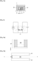
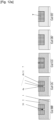
- FIG. 1 schematically represents two sectional views of Semi-Insulating Buried Heterostructures (SIBH) realized by a state-of-the-art one-step process of manufacture.
- SIBH Semi-Insulating Buried Heterostructures
- FIG. 1 shows that a metal contact 8 is deposited on a p-doped III-V semiconductor 4 and/or on the front side of the n doped III-V semi-conductor 2 (see FIG. 1 , right scheme).
- the last solution implies the etching of a via 70 in the SIBH layer 7 until reaching a doped III-V layer 2 connected to the III-V substrate 1.
- FIG. 2 schematically represents two sectional views of the Semi-Insulating Buried Heterostructures (SIBH) of FIG. 1 in which pillars 71, 72 are generated for obtaining structures with metal contacts 8 at the same level, one of the structures being encapsulated in a resin R for overcoming mechanical weakness issues (see FIG. 2 , right scheme 2). However, it generates a thermal resistivity. A bad heat evacuation strongly penalizes the performances of the chip.
- SIBH Semi-Insulating Buried Heterostructures
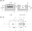
- FIGs. 3a to 3c schematically represent two specific embodiments (respectively corresponding to an embodiment with a narrow waveguide PIN and to an embodiment with a large PIN waveguide) of an integrated optoelectronic device D according to the present invention that overcomes the above-mentioned drawbacks.
- the figures show:
- FIGs. 3a and 3b show that it comprises:
- FIG. 3a shows that an anti-reflective coating 10 (Rmin) is deposited on the front face of the device D to obtain a good coupling between the incident optical signal (represented by a left thick arrow) and the device D. It is realized with dielectric layers like Al 2 O 3 , TiO 2 and SiO 2 , whose thickness are adjusted to permit this low optical reflectivity.
- Rmin anti-reflective coating 10
- FIG. 3b shows that the p and n contact are on the upper side of the wafer at the same level.
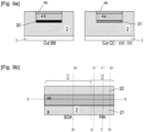
- FIGs. 3b2 and 3b3 correspond respectively to the vertical cut of the PIN section (IIa) with a large optical wave guide (cut CC on figure 3a ) and the vertical cut of the PIN section with a narrow optical wave guide (cut CC on figure 3a ).
- FIG. 3c shows an embodiment with metal contacts 81, 82, 83, 84 soldered on the flip-chip package F.
- the mechanical weakness is thus suppressed.
- Minimizing the wire bonding permits to limit the Joule effect due to the current intensity and to limit parasitic electric impedance.
- the heat produced by the photon generation in the SOA (zone I) and the photon detection in the PIN (zone IIb) can be easily evacuated because there is no resin generating a thermal resistivity.
- the opto-electronic device D thus comprises a semiconductor optical amplifier (SOA - zone I) working in a continuous wave condition and a PIN photodiode (zone IIb), able to detect high frequencies amplified incident optical signals.
- SOA amplification pushes the PIN performances to its limits with yet small optical power.
- the integration of the optical functions is based on a butt-joint technology. By this way, Multiple Quantum Wells can be optimized in every optical function.
- An H+ implantation 9 is localized to separate electrically the direct-biased SOA I from the reverse-biased PIN IIb.
- FIG. 4 schematically represents the electrical scheme or equivalent circuit of the SOA-PIN device D: the SOA function (in zone I) is powered by a current generator and the PIN function (in zone IIb) is polarized by a voltage generator. Both current generator and voltage generator are external to the device D and can be connected to the devices using the contact layers.
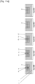
- FIGs. 5 to 13 together with the above-described FIG. 3 schematically represent the different steps of the process flow for fabricating an opto-electronic device D according to the embodiments represented in figure 3 .
- FIG. 5 schematically represents step A to C; being composed in detail of:
- FIG. 6 represents step D to E being composed in detail of:
- a second dielectric mask 62 is formed (step F') for covering at least the layer of p-doped III-V semi-conductor material 4 to form a second masked stack 62', the remaining zone constituting the second zone II ( FIG. 7a , left part).
- the second stack covered with a mask 62' is etched down to the level of the first groove 201 to form a second groove 202 (step G) with a U-shaped cross section of width W ( FIG. 7a , left part).
- FIG. 8 shows that step G is followed by the epitaxial growing of a second active material stack 31' within the second zone II, to fill said second groove 202 on the layer of the n-doped III-V semi-conductor 2 (step H), this second active material stack 31' being in line with the first active material stack 30' ( FIG. 7a , right part).
- step H is followed by the performing an epitaxial growth of p-doped III-V semi-conductor material 4 comprising at least a p-InP layer 4a and a p-doped III-V semi-conductor contact layer 4b (step I) to fill the second groove 202 on the second active material stack 31' up to at least the level of the top of the side walls 21, 22.
- FIG. 9 schematically represents step I', wherein the remaining portions of the first and second dielectric masks 61, 62 are removed (step K). Then a third dielectric mask 63 is formed so as to cover at least the top surface of the first and second zones I and II (this step is not illustrated in figure 9 ).
- FIG. 10 shows that, within said second zone II, a first pair of longitudinal channels C1, C2 is etched at least below the level of the first active material stack 30' (step J), each channel being located along each side wall 21, 22 so as to define a first central stripe portion S1 of width w S1 comprising the etched first active material stack 30 constituting the optical waveguide SOA 3) and the etched layer of p-doped III-V semi-conductor material 4, the first zone (I) constituting the SOA zone.
- FIG. 10 also shows that, within the second zone II, a network of grooves C3, C4, C5, C6 having an H-shaped top cut is etched along the longitudinal axis XX at least below the level of the second active material stack 31', said network of grooves C3, C4, C5, C6 , said network of grooves C3, C4, C5, C6 comprising (step K): a second pair of longitudinal channels C3, C4, each located along each side wall 21, 22 so as to define a second central stripe portion S2 of width w s2 comprising the etched second active material stack 31' constituting the optical waveguide PIN 31 and the etched layer of p-doped III-V semi-conductor material 4, all together forming the PIN zone IIa,
- the stripes can have different widths in function of the optical functions (see FIG. 10 , and also below FIG. 11 ). It is particularly interesting to define a narrow optical guide (having a width W S2 comprised between 0,5 ⁇ m and 2 ⁇ mm) in the PIN section (IIa) in order to limit the capacitance of the PIN. This case is illustrated in the third vertical cut according the CC plan and second overview sketch of FIG. 10a .
- the SOA and the PIN can be connected by n and p InP (n-doped III-V semiconductor and p-doped III-V semiconductor in figure 4f), but it is more advantageous to etch the interconnection (IIb) and to fill the cavity C5 with semi insulating InP, in order to improve the PIN capacitance.
- the insulated section is processed for the future modulation electrical contact of the PIN.
- FIG.11 shows the next step L, in which, inside the first pair of longitudinal channels C1, C2 and the network of grooves C3, C4, C5, C6, a semi-insulating stack 7 (such as InP) is regrown up to at least the level of the top of the layer of p-doped III-V semi-conductor 4.
- a semi-insulating stack 7 such as InP
- step L' see FIG. 12 .
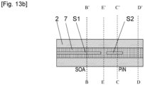
- a step L" of chemical and/or mechanical surface stripping of the regrown semi-insulating stack 7 may be performed, to flatten it to the level of the top of the side walls 21, 22, inside the first pair of longitudinal channels C1, C2 and the network of grooves C3, C4, C5, C6, a semi-insulating stack 7 up is regrown to at least the level of the top of the layer of p-doped III-V semi-conductor 4 (see FIG. 13 ).
- FIG. 3 shows the two last steps of the process of fabrication which comprises:
- the metal contacts 81, 82, 83, 84 must stays on the p-semiconductor 2and the semi insulating InP 7 to avoid an electric short cut between the p and n semiconductors.
- the high frequency capacitance is only limited by the width of the p-semiconductor 2.
Landscapes
- Physics & Mathematics (AREA)
- Condensed Matter Physics & Semiconductors (AREA)
- General Physics & Mathematics (AREA)
- Electromagnetism (AREA)
- Optics & Photonics (AREA)
- Geometry (AREA)
- Light Receiving Elements (AREA)
Priority Applications (1)
| Application Number | Priority Date | Filing Date | Title |
|---|---|---|---|
| EP22305017.0A EP4210185B1 (de) | 2022-01-10 | 2022-01-10 | Integrierte optoelektronische vorrichtung zur flip-chip-integration |
Applications Claiming Priority (1)
| Application Number | Priority Date | Filing Date | Title |
|---|---|---|---|
| EP22305017.0A EP4210185B1 (de) | 2022-01-10 | 2022-01-10 | Integrierte optoelektronische vorrichtung zur flip-chip-integration |
Publications (2)
| Publication Number | Publication Date |
|---|---|
| EP4210185A1 true EP4210185A1 (de) | 2023-07-12 |
| EP4210185B1 EP4210185B1 (de) | 2025-10-22 |
Family
ID=79831551
Family Applications (1)
| Application Number | Title | Priority Date | Filing Date |
|---|---|---|---|
| EP22305017.0A Active EP4210185B1 (de) | 2022-01-10 | 2022-01-10 | Integrierte optoelektronische vorrichtung zur flip-chip-integration |
Country Status (1)
| Country | Link |
|---|---|
| EP (1) | EP4210185B1 (de) |
Cited By (1)
| Publication number | Priority date | Publication date | Assignee | Title |
|---|---|---|---|---|
| US20230117332A1 (en) * | 2021-10-14 | 2023-04-20 | Lumentum Japan, Inc. | Semiconductor optical integrated device |
Citations (5)
| Publication number | Priority date | Publication date | Assignee | Title |
|---|---|---|---|---|
| US4954786A (en) * | 1989-01-12 | 1990-09-04 | Kabushiki Kaisha Toshiba | Optical amplifying device |
| US20050025414A1 (en) * | 2003-07-30 | 2005-02-03 | Opnext Japan, Inc. | Semiconductor optical amplifier, and optical module using the same |
| US20050259708A1 (en) * | 2004-05-20 | 2005-11-24 | Park Byeong-Hoon | Photonic integrated device using reverse-mesa structure and method for fabricating the same |
| EP3416252A1 (de) | 2017-06-13 | 2018-12-19 | Nokia Solutions and Networks Oy | Einstufige sibh für integrierte schaltungen |
| US20210066537A1 (en) * | 2019-08-26 | 2021-03-04 | Rockley Photonics Limited | Method of manufacturing a iii-v based optoelectronic device |
-
2022
- 2022-01-10 EP EP22305017.0A patent/EP4210185B1/de active Active
Patent Citations (5)
| Publication number | Priority date | Publication date | Assignee | Title |
|---|---|---|---|---|
| US4954786A (en) * | 1989-01-12 | 1990-09-04 | Kabushiki Kaisha Toshiba | Optical amplifying device |
| US20050025414A1 (en) * | 2003-07-30 | 2005-02-03 | Opnext Japan, Inc. | Semiconductor optical amplifier, and optical module using the same |
| US20050259708A1 (en) * | 2004-05-20 | 2005-11-24 | Park Byeong-Hoon | Photonic integrated device using reverse-mesa structure and method for fabricating the same |
| EP3416252A1 (de) | 2017-06-13 | 2018-12-19 | Nokia Solutions and Networks Oy | Einstufige sibh für integrierte schaltungen |
| US20210066537A1 (en) * | 2019-08-26 | 2021-03-04 | Rockley Photonics Limited | Method of manufacturing a iii-v based optoelectronic device |
Non-Patent Citations (1)
| Title |
|---|
| MASON B ET AL: "Photonic integrated receiver for 40 Gbit/s transmission", ELECTRONICS LETTERS, THE INSTITUTION OF ENGINEERING AND TECHNOLOGY, GB, vol. 38, no. 20, 26 September 2002 (2002-09-26), pages 1196 - 1197, XP006018867, ISSN: 0013-5194, DOI: 10.1049/EL:20020778 * |
Cited By (1)
| Publication number | Priority date | Publication date | Assignee | Title |
|---|---|---|---|---|
| US20230117332A1 (en) * | 2021-10-14 | 2023-04-20 | Lumentum Japan, Inc. | Semiconductor optical integrated device |
Also Published As
| Publication number | Publication date |
|---|---|
| EP4210185B1 (de) | 2025-10-22 |
Similar Documents
| Publication | Publication Date | Title |
|---|---|---|
| CN113396486B (zh) | 具有电介质dbr的磷化铟vcsel | |
| US5987046A (en) | Optical semiconductor device and a method of manufacturing the same | |
| US10985524B1 (en) | High-power hybrid silicon-photonics laser | |
| US20200335940A1 (en) | High-order bragg grating single-mode laser array | |
| WO1992005576A1 (en) | New structure and method for fabricating indium phosphide/indium gallium arsenide phosphide buried heterostructure semiconductor lasers | |
| JP3230785B2 (ja) | 半導体レーザおよびその製造方法 | |
| JP5185892B2 (ja) | 半導体光素子、及びその製造方法 | |
| US11670908B2 (en) | Planar laser structure with vertical signal transition | |
| CN112670823B (zh) | 电吸收调制激光器的制作方法 | |
| EP4210185B1 (de) | Integrierte optoelektronische vorrichtung zur flip-chip-integration | |
| US6931041B2 (en) | Integrated semiconductor laser device and method of manufacture thereof | |
| US6509580B2 (en) | Semiconductor device with current confinement structure | |
| JPH03256386A (ja) | 半導体レーザ、その製造方法及び光通信システム | |
| US10461495B2 (en) | Substrate technology for quantum dot lasers integrated on silicon | |
| EP4210184B1 (de) | Elektroabsorptionsmodulierte laservorrichtung zur flip-chip-integration | |
| US5351258A (en) | Semiconductor laser device | |
| US5346854A (en) | Method of making a semiconductor laser | |
| CN109638648B (zh) | 电注入硅基iii-v族边发射纳米线激光器及其制备方法 | |
| US5222091A (en) | Structure for indium phosphide/indium gallium arsenide phosphide buried heterostructure semiconductor | |
| CN112042069A (zh) | 光学半导体元件及其制造方法以及光学集成半导体元件及其制造方法 | |
| US20020158314A1 (en) | Buried mesa semiconductor device | |
| US11539188B2 (en) | Surface emitting laser and method of manufacturing the same | |
| US6937632B2 (en) | Integrated semiconductor laser and waveguide device | |
| US20210375963A1 (en) | Image sensor and electronic device | |
| US20250309609A1 (en) | Semiconductor optical device and method of manufacturing semiconductor optical device |
Legal Events
| Date | Code | Title | Description |
|---|---|---|---|
| PUAI | Public reference made under article 153(3) epc to a published international application that has entered the european phase |
Free format text: ORIGINAL CODE: 0009012 |
|
| STAA | Information on the status of an ep patent application or granted ep patent |
Free format text: STATUS: THE APPLICATION HAS BEEN PUBLISHED |
|
| AK | Designated contracting states |
Kind code of ref document: A1 Designated state(s): AL AT BE BG CH CY CZ DE DK EE ES FI FR GB GR HR HU IE IS IT LI LT LU LV MC MK MT NL NO PL PT RO RS SE SI SK SM TR |
|
| STAA | Information on the status of an ep patent application or granted ep patent |
Free format text: STATUS: REQUEST FOR EXAMINATION WAS MADE |
|
| 17P | Request for examination filed |
Effective date: 20231012 |
|
| RBV | Designated contracting states (corrected) |
Designated state(s): AL AT BE BG CH CY CZ DE DK EE ES FI FR GB GR HR HU IE IS IT LI LT LU LV MC MK MT NL NO PL PT RO RS SE SI SK SM TR |
|
| GRAP | Despatch of communication of intention to grant a patent |
Free format text: ORIGINAL CODE: EPIDOSNIGR1 |
|
| STAA | Information on the status of an ep patent application or granted ep patent |
Free format text: STATUS: GRANT OF PATENT IS INTENDED |
|
| INTG | Intention to grant announced |
Effective date: 20250605 |
|
| GRAS | Grant fee paid |
Free format text: ORIGINAL CODE: EPIDOSNIGR3 |
|
| GRAA | (expected) grant |
Free format text: ORIGINAL CODE: 0009210 |
|
| STAA | Information on the status of an ep patent application or granted ep patent |
Free format text: STATUS: THE PATENT HAS BEEN GRANTED |
|
| AK | Designated contracting states |
Kind code of ref document: B1 Designated state(s): AL AT BE BG CH CY CZ DE DK EE ES FI FR GB GR HR HU IE IS IT LI LT LU LV MC MK MT NL NO PL PT RO RS SE SI SK SM TR |
|
| REG | Reference to a national code |
Ref country code: CH Ref legal event code: F10 Free format text: ST27 STATUS EVENT CODE: U-0-0-F10-F00 (AS PROVIDED BY THE NATIONAL OFFICE) Effective date: 20251022 Ref country code: GB Ref legal event code: FG4D |
|
| REG | Reference to a national code |
Ref country code: DE Ref legal event code: R096 Ref document number: 602022023425 Country of ref document: DE |
|
| REG | Reference to a national code |
Ref country code: IE Ref legal event code: FG4D |
|
| PGFP | Annual fee paid to national office [announced via postgrant information from national office to epo] |
Ref country code: FR Payment date: 20251208 Year of fee payment: 5 |
|
| REG | Reference to a national code |
Ref country code: NL Ref legal event code: MP Effective date: 20251022 |
|
| PG25 | Lapsed in a contracting state [announced via postgrant information from national office to epo] |
Ref country code: NL Free format text: LAPSE BECAUSE OF FAILURE TO SUBMIT A TRANSLATION OF THE DESCRIPTION OR TO PAY THE FEE WITHIN THE PRESCRIBED TIME-LIMIT Effective date: 20251022 |