EP4210184B1 - Electro-absorption modulated laser device for flip-chip integration - Google Patents
Electro-absorption modulated laser device for flip-chip integration Download PDFInfo
- Publication number
- EP4210184B1 EP4210184B1 EP22305015.4A EP22305015A EP4210184B1 EP 4210184 B1 EP4210184 B1 EP 4210184B1 EP 22305015 A EP22305015 A EP 22305015A EP 4210184 B1 EP4210184 B1 EP 4210184B1
- Authority
- EP
- European Patent Office
- Prior art keywords
- zone
- semi
- doped iii
- longitudinal axis
- layer
- Prior art date
- Legal status (The legal status is an assumption and is not a legal conclusion. Google has not performed a legal analysis and makes no representation as to the accuracy of the status listed.)
- Active
Links
- 238000010521 absorption reaction Methods 0.000 title claims description 16
- 230000010354 integration Effects 0.000 title description 2
- 239000004065 semiconductor Substances 0.000 claims description 56
- 238000000926 separation method Methods 0.000 claims description 21
- 239000000758 substrate Substances 0.000 claims description 17
- 238000005530 etching Methods 0.000 claims description 15
- 239000002184 metal Substances 0.000 claims description 13
- 238000004519 manufacturing process Methods 0.000 claims description 12
- 238000000034 method Methods 0.000 claims description 12
- 230000003287 optical effect Effects 0.000 claims description 12
- 239000000463 material Substances 0.000 claims description 9
- 239000011149 active material Substances 0.000 claims description 7
- 230000012010 growth Effects 0.000 claims description 7
- 150000002500 ions Chemical class 0.000 claims description 6
- 238000000151 deposition Methods 0.000 claims description 5
- 239000000126 substance Substances 0.000 claims description 3
- 238000005516 engineering process Methods 0.000 description 5
- 230000005693 optoelectronics Effects 0.000 description 5
- 239000011347 resin Substances 0.000 description 3
- 229920005989 resin Polymers 0.000 description 3
- 229910000530 Gallium indium arsenide Inorganic materials 0.000 description 2
- 230000005540 biological transmission Effects 0.000 description 2
- 238000010420 art technique Methods 0.000 description 1
- 230000008033 biological extinction Effects 0.000 description 1
- 238000010276 construction Methods 0.000 description 1
- 239000006185 dispersion Substances 0.000 description 1
- 230000000694 effects Effects 0.000 description 1
- 238000000407 epitaxy Methods 0.000 description 1
- 238000005468 ion implantation Methods 0.000 description 1
- 238000002955 isolation Methods 0.000 description 1
- 230000003071 parasitic effect Effects 0.000 description 1
- 230000001629 suppression Effects 0.000 description 1
Images


Classifications
-
- H—ELECTRICITY
- H01—ELECTRIC ELEMENTS
- H01S—DEVICES USING THE PROCESS OF LIGHT AMPLIFICATION BY STIMULATED EMISSION OF RADIATION [LASER] TO AMPLIFY OR GENERATE LIGHT; DEVICES USING STIMULATED EMISSION OF ELECTROMAGNETIC RADIATION IN WAVE RANGES OTHER THAN OPTICAL
- H01S5/00—Semiconductor lasers
- H01S5/02—Structural details or components not essential to laser action
- H01S5/026—Monolithically integrated components, e.g. waveguides, monitoring photo-detectors, drivers
- H01S5/0265—Intensity modulators
-
- H—ELECTRICITY
- H01—ELECTRIC ELEMENTS
- H01S—DEVICES USING THE PROCESS OF LIGHT AMPLIFICATION BY STIMULATED EMISSION OF RADIATION [LASER] TO AMPLIFY OR GENERATE LIGHT; DEVICES USING STIMULATED EMISSION OF ELECTROMAGNETIC RADIATION IN WAVE RANGES OTHER THAN OPTICAL
- H01S5/00—Semiconductor lasers
- H01S5/005—Optical components external to the laser cavity, specially adapted therefor, e.g. for homogenisation or merging of the beams or for manipulating laser pulses, e.g. pulse shaping
-
- H—ELECTRICITY
- H01—ELECTRIC ELEMENTS
- H01S—DEVICES USING THE PROCESS OF LIGHT AMPLIFICATION BY STIMULATED EMISSION OF RADIATION [LASER] TO AMPLIFY OR GENERATE LIGHT; DEVICES USING STIMULATED EMISSION OF ELECTROMAGNETIC RADIATION IN WAVE RANGES OTHER THAN OPTICAL
- H01S5/00—Semiconductor lasers
- H01S5/02—Structural details or components not essential to laser action
- H01S5/0206—Substrates, e.g. growth, shape, material, removal or bonding
- H01S5/0207—Substrates having a special shape
-
- H—ELECTRICITY
- H01—ELECTRIC ELEMENTS
- H01S—DEVICES USING THE PROCESS OF LIGHT AMPLIFICATION BY STIMULATED EMISSION OF RADIATION [LASER] TO AMPLIFY OR GENERATE LIGHT; DEVICES USING STIMULATED EMISSION OF ELECTROMAGNETIC RADIATION IN WAVE RANGES OTHER THAN OPTICAL
- H01S5/00—Semiconductor lasers
- H01S5/02—Structural details or components not essential to laser action
- H01S5/022—Mountings; Housings
- H01S5/0233—Mounting configuration of laser chips
- H01S5/0234—Up-side down mountings, e.g. Flip-chip, epi-side down mountings or junction down mountings
-
- H—ELECTRICITY
- H01—ELECTRIC ELEMENTS
- H01S—DEVICES USING THE PROCESS OF LIGHT AMPLIFICATION BY STIMULATED EMISSION OF RADIATION [LASER] TO AMPLIFY OR GENERATE LIGHT; DEVICES USING STIMULATED EMISSION OF ELECTROMAGNETIC RADIATION IN WAVE RANGES OTHER THAN OPTICAL
- H01S5/00—Semiconductor lasers
- H01S5/04—Processes or apparatus for excitation, e.g. pumping, e.g. by electron beams
- H01S5/042—Electrical excitation ; Circuits therefor
- H01S5/0425—Electrodes, e.g. characterised by the structure
- H01S5/04256—Electrodes, e.g. characterised by the structure characterised by the configuration
- H01S5/04257—Electrodes, e.g. characterised by the structure characterised by the configuration having positive and negative electrodes on the same side of the substrate
-
- H—ELECTRICITY
- H01—ELECTRIC ELEMENTS
- H01S—DEVICES USING THE PROCESS OF LIGHT AMPLIFICATION BY STIMULATED EMISSION OF RADIATION [LASER] TO AMPLIFY OR GENERATE LIGHT; DEVICES USING STIMULATED EMISSION OF ELECTROMAGNETIC RADIATION IN WAVE RANGES OTHER THAN OPTICAL
- H01S5/00—Semiconductor lasers
- H01S5/10—Construction or shape of the optical resonator, e.g. extended or external cavity, coupled cavities, bent-guide, varying width, thickness or composition of the active region
- H01S5/12—Construction or shape of the optical resonator, e.g. extended or external cavity, coupled cavities, bent-guide, varying width, thickness or composition of the active region the resonator having a periodic structure, e.g. in distributed feedback [DFB] lasers
-
- H—ELECTRICITY
- H01—ELECTRIC ELEMENTS
- H01S—DEVICES USING THE PROCESS OF LIGHT AMPLIFICATION BY STIMULATED EMISSION OF RADIATION [LASER] TO AMPLIFY OR GENERATE LIGHT; DEVICES USING STIMULATED EMISSION OF ELECTROMAGNETIC RADIATION IN WAVE RANGES OTHER THAN OPTICAL
- H01S5/00—Semiconductor lasers
- H01S5/20—Structure or shape of the semiconductor body to guide the optical wave ; Confining structures perpendicular to the optical axis, e.g. index or gain guiding, stripe geometry, broad area lasers, gain tailoring, transverse or lateral reflectors, special cladding structures, MQW barrier reflection layers
- H01S5/22—Structure or shape of the semiconductor body to guide the optical wave ; Confining structures perpendicular to the optical axis, e.g. index or gain guiding, stripe geometry, broad area lasers, gain tailoring, transverse or lateral reflectors, special cladding structures, MQW barrier reflection layers having a ridge or stripe structure
- H01S5/2205—Structure or shape of the semiconductor body to guide the optical wave ; Confining structures perpendicular to the optical axis, e.g. index or gain guiding, stripe geometry, broad area lasers, gain tailoring, transverse or lateral reflectors, special cladding structures, MQW barrier reflection layers having a ridge or stripe structure comprising special burying or current confinement layers
- H01S5/2222—Structure or shape of the semiconductor body to guide the optical wave ; Confining structures perpendicular to the optical axis, e.g. index or gain guiding, stripe geometry, broad area lasers, gain tailoring, transverse or lateral reflectors, special cladding structures, MQW barrier reflection layers having a ridge or stripe structure comprising special burying or current confinement layers having special electric properties
- H01S5/2224—Structure or shape of the semiconductor body to guide the optical wave ; Confining structures perpendicular to the optical axis, e.g. index or gain guiding, stripe geometry, broad area lasers, gain tailoring, transverse or lateral reflectors, special cladding structures, MQW barrier reflection layers having a ridge or stripe structure comprising special burying or current confinement layers having special electric properties semi-insulating semiconductors
-
- H—ELECTRICITY
- H01—ELECTRIC ELEMENTS
- H01S—DEVICES USING THE PROCESS OF LIGHT AMPLIFICATION BY STIMULATED EMISSION OF RADIATION [LASER] TO AMPLIFY OR GENERATE LIGHT; DEVICES USING STIMULATED EMISSION OF ELECTROMAGNETIC RADIATION IN WAVE RANGES OTHER THAN OPTICAL
- H01S5/00—Semiconductor lasers
- H01S5/20—Structure or shape of the semiconductor body to guide the optical wave ; Confining structures perpendicular to the optical axis, e.g. index or gain guiding, stripe geometry, broad area lasers, gain tailoring, transverse or lateral reflectors, special cladding structures, MQW barrier reflection layers
- H01S5/22—Structure or shape of the semiconductor body to guide the optical wave ; Confining structures perpendicular to the optical axis, e.g. index or gain guiding, stripe geometry, broad area lasers, gain tailoring, transverse or lateral reflectors, special cladding structures, MQW barrier reflection layers having a ridge or stripe structure
- H01S5/227—Buried mesa structure ; Striped active layer
- H01S5/2275—Buried mesa structure ; Striped active layer mesa created by etching
-
- H—ELECTRICITY
- H01—ELECTRIC ELEMENTS
- H01S—DEVICES USING THE PROCESS OF LIGHT AMPLIFICATION BY STIMULATED EMISSION OF RADIATION [LASER] TO AMPLIFY OR GENERATE LIGHT; DEVICES USING STIMULATED EMISSION OF ELECTROMAGNETIC RADIATION IN WAVE RANGES OTHER THAN OPTICAL
- H01S5/00—Semiconductor lasers
- H01S5/02—Structural details or components not essential to laser action
- H01S5/028—Coatings ; Treatment of the laser facets, e.g. etching, passivation layers or reflecting layers
- H01S5/0287—Facet reflectivity
-
- H—ELECTRICITY
- H01—ELECTRIC ELEMENTS
- H01S—DEVICES USING THE PROCESS OF LIGHT AMPLIFICATION BY STIMULATED EMISSION OF RADIATION [LASER] TO AMPLIFY OR GENERATE LIGHT; DEVICES USING STIMULATED EMISSION OF ELECTROMAGNETIC RADIATION IN WAVE RANGES OTHER THAN OPTICAL
- H01S5/00—Semiconductor lasers
- H01S5/10—Construction or shape of the optical resonator, e.g. extended or external cavity, coupled cavities, bent-guide, varying width, thickness or composition of the active region
- H01S5/12—Construction or shape of the optical resonator, e.g. extended or external cavity, coupled cavities, bent-guide, varying width, thickness or composition of the active region the resonator having a periodic structure, e.g. in distributed feedback [DFB] lasers
- H01S5/125—Distributed Bragg reflector [DBR] lasers
Definitions
- Various example embodiments relate to optoelectronic devices such as Electro-absorption Modulated Lasers (usually known by the acronym EML).
- EML Electro-absorption Modulated Lasers
- embodiments according to the invention relate to the realization of such optoelectronic devices which are based on an one-step process of a Semi-insulated Buried Heterostructure (usually known by the acronym SiBH).
- an EML is a laser diode integrated with an electro-absorption modulator (usually known by the acronym EAM) in a single chip. It can be applied to high frequency telecommunications (up to 100 Gbit/s) and long-distance transmission (10 km to 100 km) applications, because of its low chromatic dispersion.
- the laser diode section operates under a continuous wave condition (CW), and on/off voltage input signals are applied to the EAM section to generate optical output signals. The properties of the laser are not altered by the modulation process.
- the frequency response up to 100 GHz of an EML depends on a capacitance in the EAM section.
- the extinction in an EML is generated by the voltage modulated absorption of the EAM section.
- SiBH Semi-insulated Buried Heterostructure
- EML electro-absorbtion modulated laser
- SOA semiconductor optical amplifiers
- EP 3416252A1 teaches a simplified one-step method for making a SIBH structure allowing electrical isolation between electrodes without the need for ion implantation.
- EP 3416252A1 presents some drawbacks.
- the optoelectronic device with SiBH obtained by this technology is not flat, especially around the waveguide, because of the different growths of the [100] [110] or [111] crystalline plans.
- the metal contacts are not at the same level. It imposes to generate pillars for the via contact on the device or on the flip chip package.
- Example embodiments of the invention aim to remedy all or some of the disadvantages of the above identified prior art.
- EML electro-absorption modulated laser
- the electro-absorption modulated laser may further comprise a dielectric mirror R max positioned at the end of the first zone opposite to first electrical separation.
- the electro-absorption modulated laser may further comprise:
- Embodiments of the invention as claimed further provide a method of fabricating an electro-absorption modulated laser device (usually known by the acronym EML) comprising:
- the active material stack (such as Multi Quantum Wells based on AlGaInP or GaInAsP) can be of different natures in the first and second zones by performing Selective Area Growth epitaxy or Butt-joint Technology.
- the method of fabricating may further comprise between steps I and J, a step I' of chemical and/or mechanical surface stripping of the regrown semi-insulating stack, to flatten it to the level of the top of the side walls.
- the method may further comprise the following step to obtain an electro-absorption modulated laser device according to the first example of the general embodiment (or first embodiment): step K of forming the first electrical separation is followed by a step L of positioning a dielectric mirror R max at the end of the first zone opposite to first electrical separation.
- the method may further comprise the following steps to obtain an electro-absorption modulated laser device according to the second example of the general embodiment (or second embodiment):
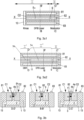
- FIG. 1 schematically represents two sectional views of Semi-Insulating Buried Heterostructures (SIBH) realized by a state-of-the-art one-step process of manufacture.
- SIBH Semi-Insulating Buried Heterostructures
- FIG. 1 shows that a p metal contact 8 is deposited on a p-doped III-V semiconductor 4 and/or on the front side of the n doped III-V semiconductor 2 (see FIG. 1 , right scheme).
- the last solution implies the etching of a via 70 in the SIBH layer 7 until reaching a doped III-V layer 2 connected to the III-V substrate 1.
- the optoelectronic device with SiBH obtained by this technology is not flat, especially around the waveguide 3, because of the different growths of the [100] [110] or [111] crystalline layers.
- FIG. 2 schematically represents the two sectional views of Semi-Insulating Buried Heterostructures (SIBH) of FIG. 1 in which pillars 71, 72 are generated for obtaining structures with metal contacts 8 at the same level, one of the structures being encapsulated in a resin R for overcoming mechanical weakness issues (see FIG. 2 , right scheme 2).
- SIBH Semi-Insulating Buried Heterostructures
- FIGs. 3a to 3c schematically represent two specific embodiments of an EML device D according to the present invention that overcomes the above-mentioned drawbacks.
- FIG. 3a shows two respective top views ( FIG. 3a1 and FIG. 3a2 ) of these two respective embodiments of the EML device D.
- FIG. 3a1 shows a first embodiment of the EML device comprising a combination of DFB laser and R max mirror and
- FIG.3a2 shows a second embodiment of the EML device comprising a combination of DFB laser and a distributed Bragg Reflector DBR.
- FIG. 3b (middle and right parts) show two sectional views of the SiBH heterostructures of these embodiments according to the B-B' and C-C' planes applying to both examples, and another sectional view (left part of Fig. 3b ) according to plane D-D' applying only to the second embodiment of FIG.3a2 ;
- FIG. 3c shows an additional sectional view of both embodiments of the EML device according to the C-C' plane, with the EML device being flip-chipped on an electronic package.
- FIGs. 3a1, 3a2 and 3b show that it comprises:
- FIG. 3c shows that the metal contacts 81, 82, 83 are soldered on the flip-chip package FP.
- the EML device thus comprises a laser working in a continuous wave condition (corresponding to the optical waveguide 3 of the first zone I) and an EAM modulated in order to reach high frequencies without a limitation of optical power (corresponding to the optical waveguide 3 in the second zone, without DFB grating or DBR).
- the optical modulated signal is emitted by the front face of the device which is at the right of Figures 3a1 and 3a2 .
- the optical functions integration is based on a single MQW layer (acronym for Multi Quantum Wells).
- the DFB grating 5a allows to define the laser wavelength.
- figure 3a1 shows that EML device D may further comprise a dielectric mirror R max 10 positioned at the end of the first zone I opposite to first electrical separation 9, that is to say on the rear face of the laser.
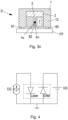
- EML device D comprises:
- FIG. 4 schematically represents the electrical scheme or equivalent circuit of the EML device: the laser function in zone I is powered by a current generator CG and the EAM function in zone II is reverse polarized by a voltage generator VG. Both current generator CG and voltage generator VG are not shown on figures 3a-c as they are lying outside of the EML laser and are connectable to the device D using the contact layers 81,82,83 .They can be made using state-of-the art techniques and be connected to the device D via cables, wires or electronic paths.
- FIGs. 5 to 10 schematically represent the different steps of the process flow for fabricating an EML device D according to the embodiments represented in figure 3 .
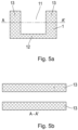
- FIG. 5a schematically represents step A of providing a substrate 1 made of III-V semiconductor material
- FIGs. 6a to 6c shows that the substrate 1 is then etched to form a groove 11 along a longitudinal axis of U-shaped cross-section and thus defining a base 12 and side walls 13 (step B) .
- a stack of layers comprising a layer of n-doped III-V semiconductor 2 on the base 1), an active material stack 3' on said layer of n-doped III-V semi-conductor 2, first p-doped III-V semiconductor 4a (such as InP),second p-doped III-V semi-conductors (such as InP and AlGaInP or GaInAsP) constituting the grating layers 5 are epitaxied (step C .
- first p-doped III-V semiconductor 4a such as InP
- second p-doped III-V semi-conductors such as InP and AlGaInP or GaInAsP
- a Distributed Feedback Grating 5a is etched in the grating layers 5 (step D), the remaining zone constituting the second zone II (for both examples: see FIGs. 6a to 6c ).
- step D may further comprise the etching of a DBR 5b inside the grating layers 5 within a first sub-zone I' located along the axis XX in the first zone I and outside the part of the first zone I containing the Distributed Feedback Grating 5a which constitutes the second sub-zone I" (for the second example only).
- step E the Distributed Bragg Reflector 5b and the Distributed Feedback Grating 5a are buried simultaneously by the layer 4 of p-doped III-V semi-conductor.
- FIG. 7 shows that step E is followed by a step G of depositing a dielectric mask 6 on the layer of p-doped III-V semi-conductor 4. This step is followed by a step H of etching, along the axis XX, two channels C1, C2 at least below the level of the active material stack 3', each channel C1, C2 being located along each side wall 13 of the substrate 1, so as to define a central stripe portion S comprising the etched material stack 3 constituting the optical waveguide 3 and the etched layer of p-doped III-V semiconductor 4.
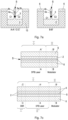
- FIGs. 8a to 8c show that a semi-insulating stack 7 is regrown at least up to the level of the top of the layer of the p-doped III-V semi-conductor contact layer 4b (step I).
- FIG. 9 shows that step I of regrowth is followed by the removing the remaining dielectric mask 6 (step J). If stack 7 is regrown over the n InP substrate, there may be an optional step J' of chemical and/or mechanical surface stripping of the stack 7, to flatten it to the level of the top of the side walls 13.
- FIG. 3a1 to c shows, for both examples of the EML device D, that metal stripes 81, 82, 83 are formed (step K) along the axis XX (see notably FIG. 3a ) and on the top of the side walls 13 and on the top of the central stripe portion (see notably FIGs. 3a1, 3a2 and 3b ).
- Step K is followed (for both embodiments: see FIGs. 3b and 3c ) by step L of forming a first electrical separation 9 between the first I and second zones II by implanting H+ ions within a thin ribbon of implanted H+ located between the side walls 13 and perpendicular to the axis XX.
- the step L of forming the first electrical separation 9 may be followed by a step M of positioning a dielectric mirror R max 10 at the end of the first zone I opposite to the first electrical separation 9, so as to obtain an EML device D according to the first example of the general embodiment.
- step L further comprises the forming of a second electrical separation 11 between the first I' and the second sub-zone I" by implanting H+ ions within another thin ribbon of implanted H+ located between the side walls 13 and perpendicular to the axis XX, provided that a DBR 5' has been previously etched into the p-doped III-V semiconductor layer 4 in step F (see above).
Landscapes
- Physics & Mathematics (AREA)
- Condensed Matter Physics & Semiconductors (AREA)
- General Physics & Mathematics (AREA)
- Electromagnetism (AREA)
- Optics & Photonics (AREA)
- Geometry (AREA)
- Semiconductor Lasers (AREA)
Description
- Various example embodiments relate to optoelectronic devices such as Electro-absorption Modulated Lasers (usually known by the acronym EML). In particular, embodiments according to the invention relate to the realization of such optoelectronic devices which are based on an one-step process of a Semi-insulated Buried Heterostructure (usually known by the acronym SiBH).
- As known by those skilled in the art, an EML is a laser diode integrated with an electro-absorption modulator (usually known by the acronym EAM) in a single chip. It can be applied to high frequency telecommunications (up to 100 Gbit/s) and long-distance transmission (10 km to 100 km) applications, because of its low chromatic dispersion. The laser diode section operates under a continuous wave condition (CW), and on/off voltage input signals are applied to the EAM section to generate optical output signals. The properties of the laser are not altered by the modulation process. The frequency response up to 100 GHz of an EML depends on a capacitance in the EAM section. The extinction in an EML is generated by the voltage modulated absorption of the EAM section.
- Semi-insulated Buried Heterostructure (usually known by the acronym SiBH) is a commonly used technology for optoelectronic devices, for fast modulation components such as electro-absorbtion modulated laser (EML), semiconductor optical amplifiers (SOA), or more generally for photonic integrated circuits. In particular, the published European patent application
EP 3416252A1 teaches a simplified one-step method for making a SIBH structure allowing electrical isolation between electrodes without the need for ion implantation. - However, the technology taught by
EP 3416252A1 presents some drawbacks. Notably, The optoelectronic device with SiBH obtained by this technology is not flat, especially around the waveguide, because of the different growths of the [100] [110] or [111] crystalline plans. Moreover, the metal contacts are not at the same level. It imposes to generate pillars for the via contact on the device or on the flip chip package. - The no planarity of the device produces mechanical weakness. To avoid the last point, the general solution is to encapsulate the device in a resin R, but it generates a thermal resistivity. A bad heat evacuation strongly penalizes the performances of the chip.
- An EML device including a Distributed Feedback Grating is disclosed in
JP H10 256669 A (MITSUBISHI ) 25 September 1998 - Thus, in light of the foregoing, there is a need of a device composed of a laser working in a continuous wave condition and an EAM modulated in order to reach high frequencies without a limitation of optical power, wherein the manufacture of such a device is based on a one-step process of making a semi-insulating buried heterostructure (SIBH) where the p and n contacts are at the same level on the same wafer face and can be easily soldered to the package of the flip-chip package.
- Example embodiments of the invention aim to remedy all or some of the disadvantages of the above identified prior art.
- The embodiments and features, if any, described in this specification that do not fall under the scope of the independent claims are to be interpreted as examples useful for understanding various embodiments of the invention.
- A general embodiment of the invention as claimed relates to an electro-absorption modulated laser (hereinafter referred to as the acronym EML) device comprising:
- a substrate made of III-V semiconductor material presenting a base and side walls and having a longitudinal axis XX, said substrate being etched to form a groove (11) of U-shaped cross-section,
- a layer of n-doped III-V semi-conductor disposed on the base inside said groove;
- a central stripe portion comprising a buried waveguide on which is grown a layer of p-doped III-V semi-conductor and a p-doped III-V semi-conductor contact layer (such as p-GaInAs) at least up to the level of the top of the side walls.
- two channels etched into the n-doped III-V semiconductor layer along the longitudinal axis XX and being located along each side wall on both sides of the central stripe portion, said channels being each filled by a regrown semi-insulating stack up to the level of the top of the the p-doped III-V semi-conductor contact layer;
- within a zone of the central stripe portion alongside the longitudinal axis XX constituting the first zone (I), a Distributed Feedback Grating (usually known a DFB grating) etched inside the layer of p-doped III-V semi-conductor, the remaining zone constituting the second zone.
- metal stripes (disposed on the top of the side walls and on the top of said the stripe portion;
- a first electrical separation (9) between the first I and second zones II consisting in a thin ribbon of implanted H+ located between the side walls and perpendicular to longitudinal axis XX.
- The device of the general embodiment presents the following advantages:
- suppression of the mechanical weakness,
- minimizing the wire bonding thus permitting to limit the Joule effect due to the current intensity and also parasitic capacitance or inductance limiting the optical high speed data transmission,
- easy evacuation of the heat produced by the photon generation in the laser and the photon modulation in the EAM because of the no presence of resin generating a thermal resistivity.
- According to a first example of the general embodiment (hereinafter referred to as first embodiment), the electro-absorption modulated laser may further comprise a dielectric mirror Rmax positioned at the end of the first zone opposite to first electrical separation.
- According to a second example of the general embodiment hereinafter referred to as second embodiment, the electro-absorption modulated laser may further comprise:
- a distributed Bragg Reflector (usually abbreviated by DBR) etched inside the layer of p-doped III-V semi-conductor within a first sub-zone located along said longitudinal axis XX in the first zone and outside the part of the first zone containing the Distributed Feedback Grating which constitutes the second sub-zone; and
- a second electrical separation between the first (I') and second sub-zoned consisting in another thin ribbon of implanted H+ located between the side walls and perpendicular to longitudinal axis XX.
- Embodiments of the invention as claimed further provide a method of fabricating an electro-absorption modulated laser device (usually known by the acronym EML) comprising:
- A. providing a substrate made of III-V semiconductor material with a longitudinal axis XX,
- B. etching said substrate to form a groove of U-shaped cross-section and thus to define a base and side walls;
- C. performing an epitaxial growth of a stack of layers comprising a layer of n-doped III-V semi-conductor on the base, an active material stack (such as Multi quantum Wells based on AlGaInP or GaInAsP) on said layer of n-doped III-V semi-conductor, and p-doped III-V semi-conductors (such as InP and AlGaInP or GaInAsP) constituting grating layers (5) ;
- D. within a zone of electro-absorption modulated laser device alongside said longitudinal axis XX constituting the first zone, etching a Distributed Feedback Grating inside the grating layers, the remaining zone constituting the second zone,
- E. performing an epitaxial growth of a layer of p-doped III-V semi-conductor (such as InP) to bury the Distributed Feedback Grating and a p-doped III-V semi-conductor contact layer (such as p-GaInAs);
- F. depositing a dielectric mask on the layer of p-doped III-V semi-conductor;
- G. etching, along the longitudinal axis XX, two channels at least below the level of the active material stack, each channel being located along each side wall of the substrate, so as to define a central stripe portion comprising the etched material stack constituting the optical waveguide and the etched layer of p-doped III-V semi-conductor;
- H. performing an epitaxial regrowth of a semi-insulating stack up to the level of the top of the p-doped III-V semiconductor contact layer;
- I. removing the remaining dielectric mask;
- J. depositing, along said longitudinal axis XX, three metal stripes on the top of the side walls (13) and on the top of said central stripe portion;
- K. forming a first electrical separation between the first and second zones by implanting H+ ions within a thin ribbon of implanted H+ located between the side walls and perpendicular to longitudinal axis
- The active material stack (such as Multi Quantum Wells based on AlGaInP or GaInAsP) can be of different natures in the first and second zones by performing Selective Area Growth epitaxy or Butt-joint Technology.
- Advantageously, the method of fabricating may further comprise between steps I and J, a step I' of chemical and/or mechanical surface stripping of the regrown semi-insulating stack, to flatten it to the level of the top of the side walls.
- According to a first example, the method may further comprise the following step to obtain an electro-absorption modulated laser device according to the first example of the general embodiment (or first embodiment): step K of forming the first electrical separation is followed by a step L of positioning a dielectric mirror Rmax at the end of the first zone opposite to first electrical separation.
- According to a second example, the method may further comprise the following steps to obtain an electro-absorption modulated laser device according to the second example of the general embodiment (or second embodiment):
- step D may further comprise , etching of a Distributed Bragg Reflector inside the grating layers within a first sub-zone located along said longitudinal axis XX in the first zone and outside the part of the first zone containing the Distributed Feedback Grating which constitutes the second sub-zone, the etching of the Distributed Bragg Reflector and the etching of the Distributed Feedback Grating being realized simultaneously, and the burying of the Distributed Bragg Reflector and that of the Distributed Feedback Grating being realized simultaneously;
- wherein during step E), the Distributed Bragg Reflector and the Distributed Feedback Grating are buried simultaneously by the layer of p-doped III-V semiconductor; and
- wherein step K is followed by a step M of forming of a second electrical separation between the first and second sub-zone by implanting H+ ions within another ribbon of implanted H+ located between the side walls and perpendicular to longitudinal axis XX.
- Some example embodiments are now described, by way of example only, and with reference to the accompanying drawings in which:
-
FIG. 1 schematically represents two sectional views of Semi-Insulating Buried Heterostructures (SIBH) realized by a state-of-the-art one-step process of manufacture; -
FIG. 2 schematically represents these two sectional views of Semi-Insulating Buried Heterostructures (SIBH) realized by a state of the art a one-step process of manufacture in which pillars are generated for obtaining structures with metal contacts at the same level; -
FIGs. 3a1 to 3c schematically represent two embodiments of an EML device D according to the present invention; -
FIG. 4 schematically represents the electrical scheme of the EML device; -
FIGs. 5 to 10 schematically represent the different steps of the process flow for fabricating an EML device according to the embodiments represented infigures 3a-c :- ∘
FIG. 5a to 5c schematically represent steps A and B; - ∘
FIG. 6a to 6c schematically represent steps C to E; - ∘
FIG. 7a to 7c schematically represent steps F and G; - ∘
FIG. 8a to 8c schematically represent step H; - ∘
FIG. 9a to 9c schematically represent step I; - ∘
FIG. 10a to 10c schematically represent step I' - ∘ steps K, L, and L' or M are schematically shown in
figures 3a1 ,3a2 to 3c (see above).
- ∘
- The same reference number represents the same element or the same type of element on all drawings, unless stated otherwise.
- The figures and the following description illustrate specific exemplary embodiments of the invention. It will thus be appreciated that those skilled in the art will be able to devise various arrangements that, although not explicitly described or shown herein, embody the principles of the invention and are included within the scope of the invention. Furthermore, any examples described herein are intended to aid in understanding the principles of the invention and are to be construed as being without limitation to such specifically recited examples and conditions. As a result, the invention is not limited to the specific embodiments or examples described below, but by the claims.
- In the following description, well-known functions or constructions by the man skilled in the art are not described in detail since they might obscure the invention in unnecessary detail.
- In the following description of the figures, schematic representations are non-limiting and serve only for the understanding of the invention.
-
FIG. 1 schematically represents two sectional views of Semi-Insulating Buried Heterostructures (SIBH) realized by a state-of-the-art one-step process of manufacture. In particular,FIG. 1 shows thata p metal contact 8 is deposited on a p-doped III-V semiconductor 4 and/or on the front side of the n doped III-V semiconductor 2 (seeFIG. 1 , right scheme). The last solution implies the etching of a via 70 in theSIBH layer 7 until reaching a doped III-V layer 2 connected to the III-V substrate 1. The optoelectronic device with SiBH obtained by this technology is not flat, especially around thewaveguide 3, because of the different growths of the [100] [110] or [111] crystalline layers. Moreover, themetal contacts 8 are not at the same level. It imposes to generatepillars FIG. 2 (left scheme).FIG. 2 schematically represents the two sectional views of Semi-Insulating Buried Heterostructures (SIBH) ofFIG. 1 in whichpillars metal contacts 8 at the same level, one of the structures being encapsulated in a resin R for overcoming mechanical weakness issues (seeFIG. 2 , right scheme 2). However, it generates a thermal resistivity. A bad heat evacuation penalizes strongly the performances of the chip. -
FIGs. 3a to 3c schematically represent two specific embodiments of an EML device D according to the present invention that overcomes the above-mentioned drawbacks. -
FIG. 3a shows two respective top views (FIG. 3a1 and FIG. 3a2 ) of these two respective embodiments of the EML device D.FIG. 3a1 . shows a first embodiment of the EML device comprising a combination of DFB laser and Rmax mirror andFIG.3a2 shows a second embodiment of the EML device comprising a combination of DFB laser and a distributed Bragg Reflector DBR. -
FIG. 3b (middle and right parts) show two sectional views of the SiBH heterostructures of these embodiments according to the B-B' and C-C' planes applying to both examples, and another sectional view (left part ofFig. 3b ) according to plane D-D' applying only to the second embodiment ofFIG.3a2 ; -
FIG. 3c shows an additional sectional view of both embodiments of the EML device according to the C-C' plane, with the EML device being flip-chipped on an electronic package. - With respect to both examples of the EML device D,
FIGs. 3a1, 3a2 and 3b show that it comprises: - a
substrate 1 made of III-V semiconductor material presenting abase 12 andside walls 13 and having a longitudinal axis XX (seeFIG. 3a1,3a2 ), saidsubstrate 1 being etched to form agroove 11 of U-shaped cross-section (see alsoFIG. 5a ), - a layer of n-doped III-
V semi-conductor 2 disposed on thebase 12 inside said groove 11 (seeFIG. 3b and7a ); - a central stripe portion S (see
FIG 3b ) comprising a buriedwaveguide 3 on which is grown a layer of p-doped III-V semi-conductor 4a and a p-doped III-Vsemiconductor contact layer 4b at least up to the level of the top of the side walls 13 (seeFIG. 3b ); - two channels C1, C2 etched into the n-doped III-
V semiconductor layer 2 along the longitudinal axis XX and being located along eachside wall 13 on both sides of the central stripe portion S, the channels C1, C2 being each filled in by a regrownsemi-insulating stack 7 up to the level of the top of the layer of p-doped III-Vsemi-conductor contact layer 4b (seeFIG. 3b ); - within a zone of the central stripe portion (S) alongside the longitudinal axis XX constituting the first zone I, a Distributed
Feedback Grating 5a etched inside the layer of p-doped III-V semi-conductor 4, the remaining zone constituting the second zone II (seeFIG. 3a ); -
metal stripes side walls 13 and on the top of said stripe portion S (seeFIG. 3b ), these metal contacts being disposed on the upper side of the wafer at the same level; - a first
electrical separation 9 between the first I and second zones II consisting in a thin ribbon of implanted H+ located between theside walls 13 and perpendicular to longitudinal axis XX (seeFIG. 3a1,3a2 ). -
FIG. 3c shows that themetal contacts optical waveguide 3 of the first zone I) and an EAM modulated in order to reach high frequencies without a limitation of optical power (corresponding to theoptical waveguide 3 in the second zone, without DFB grating or DBR). The optical modulated signal is emitted by the front face of the device which is at the right ofFigures 3a1 and 3a2 . The optical functions integration is based on a single MQW layer (acronym for Multi Quantum Wells). The DFB grating 5a allows to define the laser wavelength. - With respect to the first example of the EML device (or first embodiment),
figure 3a1 shows that EML device D may further comprise adielectric mirror R max 10 positioned at the end of the first zone I opposite to firstelectrical separation 9, that is to say on the rear face of the laser. - With respect to the second example of the EML device (or second embodiment),
figure 3a2 and the left part offigure 3b show that EML device D comprises: - a distributed Bragg Reflector (DBR) 5b etched within a first sub-zone I' located along the longitudinal axis XX in the first zone I and outside the part of the first zone I containing the Distributed
Feedback Grating 5a which constitutes the second sub-zone (I"); and - a second
electrical separation 11 between the first I' and second sub-zone I" consisting of another thin ribbon of implanted H+ located between theside walls 13 and perpendicular to longitudinal axis XX. -
FIG. 4 schematically represents the electrical scheme or equivalent circuit of the EML device: the laser function in zone I is powered by a current generator CG and the EAM function in zone II is reverse polarized by a voltage generator VG. Both current generator CG and voltage generator VG are not shown onfigures 3a-c as they are lying outside of the EML laser and are connectable to the device D using the contact layers 81,82,83 .They can be made using state-of-the art techniques and be connected to the device D via cables, wires or electronic paths. -
FIGs. 5 to 10 schematically represent the different steps of the process flow for fabricating an EML device D according to the embodiments represented infigure 3 . - In particular,
FIG. 5a schematically represents step A of providing asubstrate 1 made of III-V semiconductor material -
FIGs. 6a to 6c shows that thesubstrate 1 is then etched to form agroove 11 along a longitudinal axis of U-shaped cross-section and thus defining abase 12 and side walls 13 (step B) . Then a stack of layers comprising a layer of n-doped III-V semiconductor 2 on the base 1), an active material stack 3' on said layer of n-doped III-V semi-conductor 2, first p-doped III-V semiconductor 4a (such as InP),second p-doped III-V semi-conductors (such as InP and AlGaInP or GaInAsP) constituting thegrating layers 5 are epitaxied (step C . - Then, within a zone of the EML device D alongside the axis XX constituting the first zone I, a Distributed
Feedback Grating 5a is etched in the grating layers 5 (step D), the remaining zone constituting the second zone II (for both examples: seeFIGs. 6a to 6c ). -
FIG. 6c shows that step D may further comprise the etching of aDBR 5b inside thegrating layers 5 within a first sub-zone I' located along the axis XX in the first zone I and outside the part of the first zone I containing the DistributedFeedback Grating 5a which constitutes the second sub-zone I" (for the second example only). - Then during step E the Distributed
Bragg Reflector 5b and the DistributedFeedback Grating 5a are buried simultaneously by thelayer 4 of p-doped III-V semi-conductor. -
FIG. 7 shows that step E is followed by a step G of depositing adielectric mask 6 on the layer of p-doped III-V semi-conductor 4. This step is followed by a step H of etching, along the axis XX, two channels C1, C2 at least below the level of the active material stack 3', each channel C1, C2 being located along eachside wall 13 of thesubstrate 1, so as to define a central stripe portion S comprising the etchedmaterial stack 3 constituting theoptical waveguide 3 and the etched layer of p-doped III-V semiconductor 4. - Then,
FIGs. 8a to 8c show that asemi-insulating stack 7 is regrown at least up to the level of the top of the layer of the p-doped III-Vsemi-conductor contact layer 4b (step I). -
FIG. 9 shows that step I of regrowth is followed by the removing the remaining dielectric mask 6 (step J). Ifstack 7 is regrown over the n InP substrate, there may be an optional step J' of chemical and/or mechanical surface stripping of thestack 7, to flatten it to the level of the top of theside walls 13. - Then
FIG. 3a1 to c shows, for both examples of the EML device D, thatmetal stripes FIG. 3a ) and on the top of theside walls 13 and on the top of the central stripe portion (see notablyFIGs. 3a1, 3a2 and 3b ). Step K is followed (for both embodiments: seeFIGs. 3b and3c ) by step L of forming a firstelectrical separation 9 between the first I and second zones II by implanting H+ ions within a thin ribbon of implanted H+ located between theside walls 13 and perpendicular to the axis XX. - According to a first example of the method of fabricating the EML device D (or first embodiment), the step L of forming the first
electrical separation 9 may be followed by a step M of positioning adielectric mirror R max 10 at the end of the first zone I opposite to the firstelectrical separation 9, so as to obtain an EML device D according to the first example of the general embodiment. - According to a second example (or second embodiment)of the method of fabricating the EML device D, step L further comprises the forming of a second
electrical separation 11 between the first I' and the second sub-zone I" by implanting H+ ions within another thin ribbon of implanted H+ located between theside walls 13 and perpendicular to the axis XX, provided that a DBR 5' has been previously etched into the p-doped III-V semiconductor layer 4 in step F (see above).
Claims (7)
- Electro-absorption modulated laser device (D) comprising:- a substrate (1) made of III-V semiconductor material presenting a base (12) and side walls (13) and having a longitudinal axis (XX), said substrate (1) being etched to form a groove (11) of U-shaped cross-section,- a layer of n-doped III-V semi-conductor (2) disposed on the base (12) inside said groove (11);- a central stripe portion (S) comprising a buried waveguide (3) on which is grown a layer of p-doped III-V semiconductor (4a) and a p-doped III-V semi-conductor contact layer (4b) at least up to the level of the top of the side walls (13);- two channels (C1, C2) etched into the n-doped III-V semiconductor layer (2) along the longitudinal axis (XX) and being located along each side wall (13) on both sides of the central stripe portion (S), said channels (C1, C2) being each filled by a regrown semi-insulating stack (7) up to the level of the top of the p-doped III-V semiconductor contact layer (4b);- within a zone of the central stripe portion (S) alongside the longitudinal axis (XX) constituting the first zone (I), a Distributed Feedback Grating (5a) etched inside the layer of p-doped III-V semi-conductor (4), the remaining zone constituting the second zone (II);- metal stripes (81, 82, 83) disposed on the top of the side walls (13) and on the top of said the stripe portion (S);- a first electrical separation (9) between the first (I) and second zones (II) consisting in a thin ribbon of implanted H+ located between the side walls (13) and perpendicular to longitudinal axis (XX).
- Electro-absorption modulated laser device (D) according to claim 1, further comprising a dielectric mirror Rmax (10) positioned at the end of the first zone (I) opposite to first electrical separation (9).
- Electro-absorption modulated laser device (D) according to anyone of claims 1 and 2, further comprising:- a distributed Bragg Reflector (DBR) (5b) etched inside the layer of p-doped III-V semi-conductor (4) within a first sub-zone (I') located along said longitudinal axis (XX) in the first zone (I) and outside the part of the first zone (I) containing the Distributed Feedback Grating (5a) which constitutes the second sub-zone (I"); and- a second electrical separation (11) between the first (I') and second sub-zoned (I") consisting in another thin ribbon of implanted H+ located between the side walls (13) and perpendicular to longitudinal axis (XX).
- Method of fabricating an electro-absorption modulated laser device (D) as defined in anyone of claims 1 to 3, said method comprising:A. providing a substrate (1) made of III-V semiconductor material with a longitudinal axis (XX),B. etching said substrate (1) to form a groove (11) of U-shaped cross-section and thus to define a base (12) and side walls (13) ;C. performing an epitaxial growth of a stack of layers comprising a layer of n-doped III-V semi-conductor (2) on the base (12), an active material stack (3') on said layer of n-doped III-V semi-conductor (2), and p-doped III-V semi-conductors (such as InP and AlGaInP or GaInAsP) constituting the grating layers (5) ;D. within a zone of electro-absorption modulated laser device (D) alongside said longitudinal axis (XX) constituting the first zone (I), etching a Distributed Feedback Grating (5a) inside the grating layers (5), the remaining zone constituting the second zone (II);E. performing an epitaxial growth of a layer (4a) of p-doped III-V semi-conductor (4a) and a p-doped III-V semi-conductor contact layer (4b) to bury said Distributed Feedback Grating (5a) ;F. depositing a dielectric mask (6) on the layer of p-doped III-V semi-conductor (4);G. etching, along the longitudinal axis (XX), two channels (C1, C2) at least below the level of the active material stack (3'), each channel (C1, C2) being located along each side wall (13) of the substrate (1), so as to define a central stripe portion (S) comprising the etched material stack (3') constituting the optical waveguide (3) and the etched layer of p-doped III-V semi-conductor (4);H. performing an epitaxial regrowth of a semi-insulating stack (7) up to the level of the top of the p-doped III-V semiconductor contact layer (4b);I. removing the remaining dielectric mask (7);J. depositing, along said longitudinal axis (XX), three metal stripes (81, 82, 83) on the top of the side walls (13) and on the top of said central stripe portion (S);K. forming a first electrical separation (9) between the first (I) and second zones (II) by implanting H+ ions within a thin ribbon of implanted H+ located between the side walls (13) and perpendicular to longitudinal axis (XX).
- Method of fabrication according to claim 4, further comprising after step K of forming the first electrical separation (9), a step L of positioning a dielectric mirror Rmax (10) at the end of the first zone (I) opposite to the first electrical separation (9) .
- Method of fabrication according to claim 4,- wherein step D further comprises, the etching of a Distributed Bragg Reflector (5b) inside the grating layers (5) within a first sub-zone (I') located along said longitudinal axis (XX) in the first zone (I) and outside the part of the first zone (I) containing the Distributed Feedback Grating (5a) which constitutes the second sub-zone (I"), the etching of the Distributed Bragg Reflector (5b) and the etching of the Distributed Feedback Grating (5a) being realized simultaneously;- wherein during step E) said Distributed Bragg Reflector (5b) and said Distributed Feedback Grating (5a) are buried simultaneously by the layer (4) of p-doped III-V semi-conductor;- wherein step K is followed by a step M of forming of a second electrical separation (11) between the first (I') and second sub-zone (I") by implanting H+ ions within another thin ribbon of implanted H+ located between the side walls (13) and perpendicular to longitudinal axis (XX).
- Method of fabrication according to anyone of claims 5 and 6, further comprising, between steps I and J, a step I' of chemical and/or mechanical surface stripping of the regrown semi-insulating stack (7), to flatten it to the level of the top of the side walls (13) .
Priority Applications (1)
| Application Number | Priority Date | Filing Date | Title |
|---|---|---|---|
| EP22305015.4A EP4210184B1 (en) | 2022-01-10 | 2022-01-10 | Electro-absorption modulated laser device for flip-chip integration |
Applications Claiming Priority (1)
| Application Number | Priority Date | Filing Date | Title |
|---|---|---|---|
| EP22305015.4A EP4210184B1 (en) | 2022-01-10 | 2022-01-10 | Electro-absorption modulated laser device for flip-chip integration |
Publications (2)
| Publication Number | Publication Date |
|---|---|
| EP4210184A1 EP4210184A1 (en) | 2023-07-12 |
| EP4210184B1 true EP4210184B1 (en) | 2024-07-24 |
Family
ID=79830952
Family Applications (1)
| Application Number | Title | Priority Date | Filing Date |
|---|---|---|---|
| EP22305015.4A Active EP4210184B1 (en) | 2022-01-10 | 2022-01-10 | Electro-absorption modulated laser device for flip-chip integration |
Country Status (1)
| Country | Link |
|---|---|
| EP (1) | EP4210184B1 (en) |
Family Cites Families (5)
| Publication number | Priority date | Publication date | Assignee | Title |
|---|---|---|---|---|
| JPH10256669A (en) * | 1997-03-14 | 1998-09-25 | Mitsubishi Electric Corp | Light modulator integrated semiconductor laser diode |
| JP2004281686A (en) * | 2003-03-14 | 2004-10-07 | Sumitomo Electric Ind Ltd | Semiconductor light emitting device and its manufacturing method |
| CN107430293B (en) * | 2015-03-23 | 2021-02-26 | 日本电信电话株式会社 | Optical circuit |
| EP3416252A1 (en) | 2017-06-13 | 2018-12-19 | Nokia Solutions and Networks Oy | One step sibh for integrated circuits |
| GB2586889B (en) * | 2019-08-26 | 2022-11-02 | Rockley Photonics Ltd | Method of manufacturing a III-V based optoelectronic device |
-
2022
- 2022-01-10 EP EP22305015.4A patent/EP4210184B1/en active Active
Also Published As
| Publication number | Publication date |
|---|---|
| EP4210184A1 (en) | 2023-07-12 |
Similar Documents
| Publication | Publication Date | Title |
|---|---|---|
| US7112827B2 (en) | Tunable wavelength laser | |
| US6238943B1 (en) | Optical semiconductor device and a method of manufacturing the same | |
| US6798807B2 (en) | Semiconductor laser and semiconductor laser module | |
| KR102171268B1 (en) | manufacturing method of Hybrid silicon laser | |
| US20070223543A1 (en) | Laterally Implanted Electroabsorption Modulated Laser | |
| US8488918B2 (en) | Semiconductor optical device, optical transmitter module, optical transceiver module, and optical transmission equipment | |
| US20200335940A1 (en) | High-order bragg grating single-mode laser array | |
| JP2001142037A (en) | Method of manufacturing field effect optical modulator and semiconductor optical element | |
| US5636237A (en) | Semiconductor laser device which makes it possible to realize high-speed modulation | |
| JP2943510B2 (en) | Tunable semiconductor laser device | |
| US11769988B2 (en) | Vertical-cavity surface-emitting laser (VCSEL) tuned through application of mechanical stress via a piezoelectric material | |
| US6931041B2 (en) | Integrated semiconductor laser device and method of manufacture thereof | |
| EP4210184B1 (en) | Electro-absorption modulated laser device for flip-chip integration | |
| US5346854A (en) | Method of making a semiconductor laser | |
| US20030137023A1 (en) | Optoelectronic device, and method for producing an optoelectronic device | |
| US7573925B1 (en) | Semiconductor laser having a doped active layer | |
| EP4210185A1 (en) | Integrated opto-electronic device for flip-chip integration | |
| US7016558B2 (en) | Integrated optical device and fabricating method thereof | |
| WO2009025912A2 (en) | Optimization of laser parameters to achieve desired performance | |
| KR20050085176A (en) | Method for manufacturing a buried tunnel junction in a surface-emitting semi-conductor laser | |
| JP2003060285A (en) | Optical integrated device | |
| EP1372229B1 (en) | Integrated semiconductor laser and waveguide device | |
| KR100584332B1 (en) | Electro-absorption modulator integrated distributed feedback laser and method for fabricating the same | |
| JP3387751B2 (en) | Semiconductor laser capable of polarization modulation and method of manufacturing the same | |
| EP4033618A1 (en) | Mach zehnder-modulated lasers |
Legal Events
| Date | Code | Title | Description |
|---|---|---|---|
| PUAI | Public reference made under article 153(3) epc to a published international application that has entered the european phase |
Free format text: ORIGINAL CODE: 0009012 |
|
| STAA | Information on the status of an ep patent application or granted ep patent |
Free format text: STATUS: THE APPLICATION HAS BEEN PUBLISHED |
|
| AK | Designated contracting states |
Kind code of ref document: A1 Designated state(s): AL AT BE BG CH CY CZ DE DK EE ES FI FR GB GR HR HU IE IS IT LI LT LU LV MC MK MT NL NO PL PT RO RS SE SI SK SM TR |
|
| STAA | Information on the status of an ep patent application or granted ep patent |
Free format text: STATUS: REQUEST FOR EXAMINATION WAS MADE |
|
| 17P | Request for examination filed |
Effective date: 20230828 |
|
| RBV | Designated contracting states (corrected) |
Designated state(s): AL AT BE BG CH CY CZ DE DK EE ES FI FR GB GR HR HU IE IS IT LI LT LU LV MC MK MT NL NO PL PT RO RS SE SI SK SM TR |
|
| GRAP | Despatch of communication of intention to grant a patent |
Free format text: ORIGINAL CODE: EPIDOSNIGR1 |
|
| STAA | Information on the status of an ep patent application or granted ep patent |
Free format text: STATUS: GRANT OF PATENT IS INTENDED |
|
| INTG | Intention to grant announced |
Effective date: 20240227 |
|
| RIN1 | Information on inventor provided before grant (corrected) |
Inventor name: GARREAU, ALEXANDRE Inventor name: PARET, JEAN FRANCOIS |
|
| GRAJ | Information related to disapproval of communication of intention to grant by the applicant or resumption of examination proceedings by the epo deleted |
Free format text: ORIGINAL CODE: EPIDOSDIGR1 |
|
| STAA | Information on the status of an ep patent application or granted ep patent |
Free format text: STATUS: REQUEST FOR EXAMINATION WAS MADE |
|
| GRAS | Grant fee paid |
Free format text: ORIGINAL CODE: EPIDOSNIGR3 |
|
| STAA | Information on the status of an ep patent application or granted ep patent |
Free format text: STATUS: GRANT OF PATENT IS INTENDED |
|
| GRAP | Despatch of communication of intention to grant a patent |
Free format text: ORIGINAL CODE: EPIDOSNIGR1 |
|
| INTC | Intention to grant announced (deleted) | ||
| INTG | Intention to grant announced |
Effective date: 20240503 |
|
| GRAA | (expected) grant |
Free format text: ORIGINAL CODE: 0009210 |
|
| STAA | Information on the status of an ep patent application or granted ep patent |
Free format text: STATUS: THE PATENT HAS BEEN GRANTED |
|
| AK | Designated contracting states |
Kind code of ref document: B1 Designated state(s): AL AT BE BG CH CY CZ DE DK EE ES FI FR GB GR HR HU IE IS IT LI LT LU LV MC MK MT NL NO PL PT RO RS SE SI SK SM TR |
|
| REG | Reference to a national code |
Ref country code: GB Ref legal event code: FG4D |
|
| REG | Reference to a national code |
Ref country code: CH Ref legal event code: EP |
|
| REG | Reference to a national code |
Ref country code: IE Ref legal event code: FG4D Ref country code: DE Ref legal event code: R096 Ref document number: 602022004836 Country of ref document: DE |