EP4208796B1 - Prioritäts-aufwärts-leveling für speicherabfrage - Google Patents
Prioritäts-aufwärts-leveling für speicherabfrage Download PDFInfo
- Publication number
- EP4208796B1 EP4208796B1 EP20816746.0A EP20816746A EP4208796B1 EP 4208796 B1 EP4208796 B1 EP 4208796B1 EP 20816746 A EP20816746 A EP 20816746A EP 4208796 B1 EP4208796 B1 EP 4208796B1
- Authority
- EP
- European Patent Office
- Prior art keywords
- memory
- request
- requests
- level
- priority
- Prior art date
- Legal status (The legal status is an assumption and is not a legal conclusion. Google has not performed a legal analysis and makes no representation as to the accuracy of the status listed.)
- Active
Links
Images



Classifications
-
- G—PHYSICS
- G06—COMPUTING OR CALCULATING; COUNTING
- G06F—ELECTRIC DIGITAL DATA PROCESSING
- G06F13/00—Interconnection of, or transfer of information or other signals between, memories, input/output devices or central processing units
- G06F13/14—Handling requests for interconnection or transfer
- G06F13/16—Handling requests for interconnection or transfer for access to memory bus
- G06F13/1605—Handling requests for interconnection or transfer for access to memory bus based on arbitration
- G06F13/161—Handling requests for interconnection or transfer for access to memory bus based on arbitration with latency improvement
- G06F13/1626—Handling requests for interconnection or transfer for access to memory bus based on arbitration with latency improvement by reordering requests
-
- G—PHYSICS
- G06—COMPUTING OR CALCULATING; COUNTING
- G06F—ELECTRIC DIGITAL DATA PROCESSING
- G06F13/00—Interconnection of, or transfer of information or other signals between, memories, input/output devices or central processing units
- G06F13/14—Handling requests for interconnection or transfer
- G06F13/16—Handling requests for interconnection or transfer for access to memory bus
- G06F13/1605—Handling requests for interconnection or transfer for access to memory bus based on arbitration
- G06F13/1642—Handling requests for interconnection or transfer for access to memory bus based on arbitration with request queuing
-
- G—PHYSICS
- G06—COMPUTING OR CALCULATING; COUNTING
- G06F—ELECTRIC DIGITAL DATA PROCESSING
- G06F13/00—Interconnection of, or transfer of information or other signals between, memories, input/output devices or central processing units
- G06F13/14—Handling requests for interconnection or transfer
- G06F13/16—Handling requests for interconnection or transfer for access to memory bus
- G06F13/1668—Details of memory controller
- G06F13/1673—Details of memory controller using buffers
Definitions
- Priority levels which affect quality of service for requesting clients, are often used for memory-request arbitration. Clients may have various requirements that dictate respective priorities of the memory requests they generate. By utilizing priority levels, the arbiter can prioritize memory requests within the memory-request buffer for granting.
- priority levels may be fixed for each memory request in the memory-request buffer. While this approach can effectively indicate that memory requests have different priorities, it cannot adapt when clients' requirements change. For example, a video card may determine that a display buffer is about to underrun and may have no means to expedite associated memory requests.
- the method includes receiving a memory request from a client over a VC and adding the memory request to a memory-request buffer along with an indication of a VCID of the VC and an original priority-level for the memory request.
- the method also includes indicating the VCID for related memory requests within the memory-request buffer.
- the method further includes determining that an up-level indication corresponding to the VCID is being asserted and, based on the up-level indication being asserted, increasing original priority-levels with the VCID indicated (e.g., the memory request and the related memory requests) to respective up-leveled priority levels.
- This document describes techniques and apparatuses that enable memory-request priority up-leveling. These techniques and apparatuses enable a client to dynamically adjust priority levels of memory requests within a memory-request buffer via a side channel to a memory controller. By asserting an up-level indication corresponding to a VCID over the side channel, the client can increase original priority-levels for memory requests within the memory-request buffer that have the VCID indicated. In some cases, the up-leveling may occur in as little as a single clock cycle. Furthermore, because the VCID is indicated for related memory requests, priority up-leveling may be achieved while accounting for memory request dependency. Although the following discussion describes acceleration of memory requests through priority up-leveling, the techniques can easily be applied to deceleration of memory requests though priority down-leveling.
- Fig. 1 illustrates a process flow 100 for adding memory requests to a memory buffer and indicating VCIDs for related memory requests.
- the process flow 100 is generally implemented in an electronic device (not shown) that is discussed below in regard to Fig. 3 .
- the process flow 100 includes a client 102 that sends a memory request 104 (e.g., read and/or write memory request) to a memory controller 106.
- the client 102 may be a component or aspect of an application, operating system, processor, core of a processor, piece of hardware, or any other entity that can generate memory requests requesting to read from or write to a memory 108.
- the memory request 104 has a VCID 110 associated with the memory request 104, an original priority-level 112, a memory address 114, and an optional transaction identification (ID) 116.
- the memory address 114 indicates a physical or virtual memory address associated with the memory request 104. Although discussed in terms of a memory address 114, the memory request 104 may include a request for a plurality of memory addresses.
- the transaction ID 116 may be included in the memory request 104 and may be used for memory request dependency, as discussed below.
- the memory request 104 is received by the memory controller 106 over a VC 118, and the VCID 110 corresponds to the VC 118.
- the VCID 110 of the memory request 104 may be inherent to the memory controller 106 based on the VC 118.
- the VC 118 may also be associated with the client.
- the VC 118 (and thus the VCID 110) may be determined based on information about the client 102 (e.g., ID, type, or location).
- the memory request 104 may explicitly contain the VCID 110 corresponding to the VC 118.
- the memory controller 106 adds the memory request 104 to a memory-request buffer 122 along with an indication of the VCID 110.
- the other memory-requests 124 have respective VCID indications 126 that were indicated upon entering the memory-request buffer 122 (similar to the memory request 104). If a related memory request exists in the memory-request buffer 122, the dependency module 120 determines if the VCID 110 is indicated for the related memory request.
- the VCID indications 126 of the other memory-requests 124 may be for the VCID 110 or other VCIDs supported by the system. For example, if the related request was received over the VC 118, then the VCID 110 may already be indicated for the related request.
- the dependency module 120 may indicate the VCID 110 for the related memory request.
- the indication of the VCID 110 for the related memory request is additive and not a replacement indication.
- the related memory request will be associated with the VCID 110 as well as a VCID for a VC over which the related memory request was received (if different than the VC 118).
- Fig. 2 illustrates an example process flow 200 for memory-request priority up-leveling.
- the process flow 200 is generally a continuation of the process flow 100 and, thus, may also be implemented in the electronic device (not shown) that is discussed below in regard to Fig. 3 .
- the process flow 200 generally occurs after the process flow 100.
- the process flow 200 occurs after the dependency module 120 has placed the memory request 104 within the memory-request buffer 122 and indicated the VCID 110 for any related requests.
- memory requests 202 include memory request 104 and the other memory-requests 124 along with their corresponding VCID indications 204 and priority levels 206.
- the up-level module 212 may consider the up-level indication 208 as being asserted until it is changed or deasserted by the client 102. Furthermore, although the same client (e.g., the client 102) as in Fig. 1 is shown, noted that the up-level indication 208 may be asserted and the up-level amount 210 set by another client. For example, the other client may have one or more memory requests 202 that were received over VC 118.
- the VCID 110 associated with the up-level indication 208 and the up-level amount 210 may, similar to the memory request 104, be inherent to the memory controller 106 based on a VC over which the up-level indication 208 is received ( e.g., a VC of the side channel 214). In such a situation, the VCID 110 may be inherent to the up-level module 212. Alternatively, the up-level indication 208 and the up-level amount 210 may be received along with an explicit indication of the VCID 110.
- Respective priority levels 206 of the memory requests 202 having the indication of the VCID 110 are increased from respective original priority-levels (e.g., original priority-level 112) to respective up-leveled priority levels based on the up-level amount 210.
- the up-level amount 210 may be a fixed amount, e.g., the priority levels 206 of the memory requests 202 having the indication of the VCID 110 are set to a specific level.
- the up-level amount 210 may be a multiplier, e.g., the priority levels 206 of the memory requests 202 having the indication of the VCID 110 are multiplied by the multiplier.
- the up-level indication 208 is a dynamic indication that can be easily asserted or deasserted by the client 102. As such, when the client 102 asserts the up-level indication 208, e.g., by setting a bit of the side channel 214, priority levels of associated requests are increased. The priority levels of the associated requests may stay increased until the up-level indication is deasserted by the client, e.g., by returning the bit. Accordingly, responsive to determining that the up-level indication 208 for the VCID 110 has been deasserted by the client 102, the up-level module 212 returns the priority levels 206 of the memory requests 202 having the indication of the VCID 110 to the respective original priority-levels.
- the up-level amount 210 can be changed dynamically by the client 102 (or another requesting client) irrespective of whether the up-level indication 208 is currently asserted and/or being received. Noted that the changes in priority levels, and thus acceleration/deceleration, may occur in as little as a single clock cycle.
- the priority levels 206 are sent to and/or viewed by an arbiter 216 that grants the memory request 104 based on the priority level of the memory request 104 (or, because priority level is only one factor for use in memory-request arbitration, the arbiter 216 may decline or defer the memory request 104).
- the arbiter 216 may grant the memory request 104 while the up-level indication 208 is asserted or deasserted. Generally, the arbiter 216 is more likely to grant the memory request 104 while the priority level of the memory request 104 is up-leveled. The memory request 104, however, may be granted after the up-level indication 208 is deasserted.
- the priority level for the memory request 104 at grant may be the original priority-level 112 or an up-leveled priority level.
- the arbiter sends a memory-request grant 218 that corresponds to the memory request 104 to the client 102.
- Other memory-requests of the memory requests 202 (including the related memory requests that are generally granted prior to the memory request 104) also have associated memory grants sent to their respective clients.
- performance of the memory controller 106 may not be affected by increasing a depth of the memory request buffer 122 (e.g., a number of memory requests able to be stored/tracked in the buffer). For example, a number of the operations discussed above may be irrespective of the depth. Furthermore, increasing the depth of the memory request buffer 122 may merely require a linear growth in area (as opposed to exponential or some other non-linear growth). Also, there may be no need to maintain additional pointers for the parent memory transactions.
- a depth of the memory request buffer 122 e.g., a number of memory requests able to be stored/tracked in the buffer. For example, a number of the operations discussed above may be irrespective of the depth.
- increasing the depth of the memory request buffer 122 may merely require a linear growth in area (as opposed to exponential or some other non-linear growth). Also, there may be no need to maintain additional pointers for the parent memory transactions.
- Fig. 3 illustrates an example electronic device 300 in which memory-request priority up-leveling can be implemented.
- the electronic device 300 is illustrated with various non-limiting examples of the electronic device 300: a smartphone 300-1, a laptop 300-2, a television 300-3, a desktop 300-4, a tablet 300-5, and a wearable device 300-6.
- the electronic device 300 includes at least one processor 302, computer-readable media 304, and the memory controller 106.
- the processor 302 executes code stored within the computer-readable media 304 to implement an operating system 306 and optionally one or more applications 308 that are stored within a storage media 310 (e.g., one or more non-transitory storage devices such as a hard drive, SSD, flash memory, read-only memory (ROM), EPROM, or EEPROM) of the computer-readable media 304.
- a storage media 310 e.g., one or more non-transitory storage devices such as a hard drive, SSD, flash memory, read-only memory (ROM), EPROM, or EEPROM
- the operating system 306 or the applications 308 generally act as the client 102, as described below, other components can also generate the memory request 104.
- the computer-readable media 304 which may be transitory or non-transitory, also includes the memory 108 (e.g., one or more non-transitory computer-readable storage devices such as a random access memory (RAM, DRAM, or SRAM)) that is requested to be accessed (e.g., read from or written to) by the client 102 through the memory request 104.
- the memory 108 e.g., one or more non-transitory computer-readable storage devices such as a random access memory (RAM, DRAM, or SRAM)
- RAM random access memory
- DRAM dynamic random access memory
- SRAM random access memory
- the memory controller 106 contains a memory-controller processor 312 and a memory controller computer-readable media 314.
- the memory-controller processor 312 e.g., an application processor, microprocessor, digital-signal processor (DSP), or controller
- DSP digital-signal processor
- the memory controller computer-readable media 314 e.g., one or more non-transitory storage devices
- the memory controller 106 also contains the arbiter 216.
- aspects of the memory controller 106 may be implemented in conjunction with the processor 302 or by the processor 302. Similarly, the memory controller 106 (or processor 302) may perform functions described herein by executing instructions that are stored within the storage media 310.
- the memory 108 and aspects of the memory controller 106 may also be combined ( e.g., implemented as part of an SoC).
- the memory controller 106 is described in terms of memory requests to access the memory 108, the techniques described herein can easily be applied for memory requests to access storage media 310.
- the memory controller 106 may be a hard drive controller, SSD controller, or the like.
- the memory controller 106 may be implemented by the processor 302 to access storage media 310.
- the electronic device 300 can include one or more communication systems (not shown) that enable wired and/or wireless communication of device data, such as received data, transmitted data, or other information as described above.
- Example communication systems include NFC transceivers, WPAN radios compliant with various IEEE 802.15 (Bluetooth TM ) standards, WLAN radios compliant with any of the various IEEE 802.11 (WiFi TM ) standards, WWAN (3GPP-compliant) radios for cellular telephony, wireless metropolitan area network (WMAN) radios compliant with various IEEE 802.16 (WiMAX TM ) standards, infrared (IR) transceivers compliant with an Infrared Data Association (IrDA) protocol, and wired local area network (LAN) Ethernet transceivers.
- aspects of the communication system may act as the client 102 by generating memory requests based on received data or data to be transmitted (e.g., a communication buffer).
- the electronic device 300 may also include one or more data input ports (not shown) by which any type of data, media content, and/or other inputs can be received (e.g., user-selectable inputs, messages, applications, music, television content, recorded video content, and any other type of audio, video, and/or image data received from any content and/or data source).
- the data input ports may include USB ports, coaxial cable ports, fiber optic ports for optical fiber interconnects or cabling, and other serial or parallel connectors (including internal connectors) for flash memory, DVDs, CDs, and the like.
- the electronic device 300 also includes an audio and/or video-processing system (not shown) that processes audio data and/or passes through the audio and video data to an audio system (not shown) and/or to a display system (not shown) (e.g., a video buffer or a screen of a smart phone or camera).
- the audio system and/or the display system may include any components that process, display, and/or otherwise render audio, video, display, and/or image data and may act as the client 102.
- Display data and audio signals can be communicated to an audio component and/or to a display component via an RF (radio frequency) link, S-video link, HDMI (high-definition multimedia interface), composite video link, component video link, DVI (digital video interface), analog audio connection, or another similar communication link, such as the media data port.
- the audio system and/or the display system are external or separate components of the electronic device 300.
- the display system can be an integrated component of the example electronic device 300, such as part of an integrated touch interface.
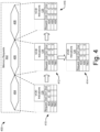
- Fig. 4 is an example illustration 400 of VCIDs being indicated for memory requests.
- the example illustration 400 shows VCID indications 126 for three memory requests 402 (memory request 404, memory request 406, and memory request 408) that are received chronologically (e.g., memory request 404 is received first, memory request 406 is received second, and memory request 408 is received third).
- the memory requests 402 are generally similar to the memory request 104 when first received and then similar to the other memory-requests 124 after the memory requests are placed in the memory-request buffer 122.
- the VCID indications 126 are shown as 0x0, 0x1, and 0x2 merely for display purposes. As discussed above, any number of VCID indications 126 in any fashion (e.g., table, vector, field, etc.) may be utilized.
- the memory request 404 is received over a VC with a VCID of 0x2.
- VCID 0x2 is indicated for the memory request 404, as shown in an example representation 410 of the memory-request buffer 122.
- the memory request 406 is received over a VC with a VCID of 0x1.
- VCID Ox1 is indicated for the memory request 406, as shown in an example representation 412 of the memory-request buffer 122.
- the memory request 406 is related to the memory request 404 (based on transaction IDs and/or memory addresses).
- the memory request 406 is determined to be dependent upon memory request 404 (e.g., memory request 406 is a child of memory request 404). Accordingly, the dependency module 120 from Fig. 1 indicates VCID 0x1 for the memory request 404, as shown in an example representation 414 of the memory-request buffer 122. As noted above, the change in VCID indications 126 for the memory request 404 may be performed prior to, concurrently with, or after the memory request 406 is added to the buffer. The change from example representation 412 to example representation 414 is merely illustrative of the change due to memory request dependency.
- the memory request 408 is received over the VC with the VCID of 0x2.
- the memory request 408 is not related to memory request 404 or 406.
- VCID 0x2 is indicated for the memory request 408, as shown in an example representation 416 of the memory-request buffer 122.
- an up-level indication for VCID 0x0 does not up-level any of the memory requests 404, 406, or 408.
- an up-level indication for VCID Ox1 up-levels the memory request 404 and the memory request 406.
- an up-level indication for VCID 0x2 up-levels the memory request 404 and the memory request 408.
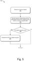
- Figs. 5 and 6 illustrate an example method 500 for memory-request priority up-leveling.
- a memory request is received.
- the memory controller 106 may receive the memory request 104 from the client 102 over a VC with the VCID 110 and may contain the original priority-level 112, the memory address 114, and optionally the transaction ID 116.
- the memory request, the VCID and the original priority-level are added to a memory-request buffer.
- the memory controller 106 may add the memory request 104 to the memory-request buffer 122 with the original priority-level 112 and the VCID 110 indicated.
- a determination that the up-level indication is being asserted for the VCID is made.
- the up-level module 212 may determine that the up-level indication 208 is being asserted for the VCID 110.
- the up-level indication may be asserted by the client that created the memory request (e.g., client 102) or another client.
- priority up-leveling can increase chances of grant
- conditions may change between when the up-level indication is asserted and a time of grant.
- a client may decide that the up-leveled priority level may be returned to the original priority-level before the memory request is granted.
- the memory request may be granted with the original priority-level.
- the process may send the priority levels to another entity that grants (or arbitrates on) the request and the other memory-requests within the memory-request buffer 122.
Landscapes
- Engineering & Computer Science (AREA)
- Theoretical Computer Science (AREA)
- Physics & Mathematics (AREA)
- General Engineering & Computer Science (AREA)
- General Physics & Mathematics (AREA)
- Bus Control (AREA)
- Communication Control (AREA)
- Information Transfer Systems (AREA)
- Memory System Of A Hierarchy Structure (AREA)
- Memory System (AREA)
Claims (14)
- Verfahren zur Prioritätsanpassung für Speicherabfragen, das durch eine Speichersteuerung (106) durchgeführt wird, wobei das Verfahren Folgendes umfasst:Empfangen (502) einer Speicherabfrage (202) von einem Client (102) über einen virtuellen Kanal (virtual channel, VC) (118), wobei die Speicherabfrage einen ursprünglichen Prioritätsgrad (112) aufweist;Hinzufügen (504) der Speicherabfrage (202) zu einem Speicherabfrage-Puffer (122) mit:einer Angabe einer vertikalen Kanalidentifizierung (virtual channel identification, VCID) (204) des VC (118); unddem ursprünglichen Prioritätsgrad (112) für die Speicherabfrage (104);Bestimmen (510), dass eine dem VCID (204) entsprechende Anpassungsangabe (208) gesetzt ist;Erhöhen (512) oder Verringern des ursprünglichen Prioritätsgrades (112) der Speicherabfrage (202) auf einen angepassten Prioritätsgrad (206) basierend auf der gesetzten Anpassungsangabe (208);Bestimmen, dass eine oder mehrere andere Speicherabfragen (124) innerhalb des Speicherabfrage-Puffers (122) eine Angabe des VCID (110) aufweisen; undErhöhen (512) oder Verringern der jeweiligen ursprünglichen Prioritätsgrade (112) der anderen Speicherabfragen (124) auf die jeweiligen Prioritätsgrade (206) basierend auf der Anpassungsangabe.
- Verfahren nach Anspruch 1, wobei die Anpassungsangabe (208) über einen Seitenkanal (214) an die Speichersteuerung (106) gesetzt wird.
- Verfahren nach Anspruch 1 oder Anspruch 2, wobei die Anpassungsangabe (208) von dem Client (102) oder einem anderen Client unter Verwendung des VC (118) gesetzt wird.
- Verfahren nach einem der vorhergehenden Ansprüche, ferner umfassend das Bestimmen eines Anpassungsbetrags (210), umfassend:einen Betrag, um den der ursprüngliche Prioritätsgrad (112) erhöht oder verringert werden soll; odereinen Wert für den angepassten Prioritätsgrad (206).
- Verfahren nach einem der vorhergehenden Ansprüche, ferner umfassend:Bestimmen (514), dass die Anpassungsangabe (208) nicht mehr gesetzt ist; undals Reaktion auf das Bestimmen, dass die Anpassungsangabe (208) nicht mehr gesetzt ist, Zurücksetzen (516) des angepassten Prioritätsgrades (206) der Speicherabfrage (104) auf den ursprünglichen Prioritätsgrad (112).
- Verfahren nach einem der vorhergehenden Ansprüche, ferner umfassend Gewähren (518) der Speicherabfrage (104) basierend auf dem angepassten Prioritätsgrad (206).
- Verfahren nach einem der vorhergehenden Ansprüche, wobei der ursprüngliche Prioritätsgrad (112) durch den Client (102) zugewiesen wird.
- Verfahren nach einem der vorhergehenden Ansprüche, wobei der VC (118) auf dem Client (102) basiert.
- Verfahren nach einem der vorhergehenden Ansprüche, ferner umfassend das Bestimmen, ob eine andere Speicherabfrage (122) in dem Speicherabfrage-Puffer (122) mit der Speicherabfrage (104) in Beziehung steht.
- Verfahren nach Anspruch 9, wobei das Bestimmen, ob eine andere Speicherabfrage (124) mit der Speicherabfrage (104) in Beziehung steht, das Vergleichen einer Transaktionsidentifizierung (116) der Speicherabfrage (104) mit entsprechenden Transaktionsidentifizierungen für andere Speicherabfragen (124) innerhalb des Speicherabfrage-Puffers (122) umfasst.
- Verfahren nach Anspruch 9, wobei das Bestimmen, ob eine weitere Speicherabfrage (124) mit der Speicherabfrage (104) in Beziehung steht, das Vergleichen einer oder mehrerer Speicheradressen (114) der Speicherabfrage (104) mit entsprechenden Speicheradressen (114) für weitere Speicherabfragen (124) innerhalb des Speicherabfrage-Puffers (122) umfasst.
- Verfahren nach Anspruch 10 oder 11, wobei die anderen Speicherabfragen (124) über einen oder mehrere VC (118) empfangen wurden, die sich von dem VC unterscheiden.
- Verfahren nach einem der Ansprüche 10 bis 12, ferner umfassend das Zuweisen des VCID (110) zu der zugehörigen Speicherabfrage, als Reaktion auf das Bestimmen (506), dass eine der anderen Speicherabfragen (124) eine zugehörige Speicherabfrage (104) ist, die zugehörig zu der Speicherabfrage ist.
- Speichersteuerung (106), die dazu konfiguriert ist, das Verfahren nach einem der vorhergehenden Ansprüche durchzuführen.
Applications Claiming Priority (1)
| Application Number | Priority Date | Filing Date | Title |
|---|---|---|---|
| PCT/US2020/059061 WO2022098356A1 (en) | 2020-11-05 | 2020-11-05 | Memory-request priority up-leveling |
Publications (2)
| Publication Number | Publication Date |
|---|---|
| EP4208796A1 EP4208796A1 (de) | 2023-07-12 |
| EP4208796B1 true EP4208796B1 (de) | 2025-06-25 |
Family
ID=73646499
Family Applications (1)
| Application Number | Title | Priority Date | Filing Date |
|---|---|---|---|
| EP20816746.0A Active EP4208796B1 (de) | 2020-11-05 | 2020-11-05 | Prioritäts-aufwärts-leveling für speicherabfrage |
Country Status (5)
| Country | Link |
|---|---|
| US (2) | US12277075B2 (de) |
| EP (1) | EP4208796B1 (de) |
| CN (1) | CN116324743A (de) |
| TW (2) | TWI787741B (de) |
| WO (1) | WO2022098356A1 (de) |
Families Citing this family (3)
| Publication number | Priority date | Publication date | Assignee | Title |
|---|---|---|---|---|
| CN116324743A (zh) | 2020-11-05 | 2023-06-23 | 谷歌有限责任公司 | 存储器请求优先级升级 |
| US20240272905A1 (en) * | 2023-02-10 | 2024-08-15 | Akeana, Inc. | Access request dynamic multilevel arbitration |
| WO2025174614A1 (en) * | 2024-02-12 | 2025-08-21 | Texas Instruments Incorporated | Hardware queue manager serving multiple processor cores |
Family Cites Families (20)
| Publication number | Priority date | Publication date | Assignee | Title |
|---|---|---|---|---|
| US20050058130A1 (en) * | 2003-08-04 | 2005-03-17 | Christ Chris B. | Method and apparatus for assigning data traffic classes to virtual channels in communications networks |
| US8690475B2 (en) * | 2010-10-05 | 2014-04-08 | Caterpillar Inc. | Compaction apparatus and associated compactor vehicle |
| US9208109B2 (en) * | 2011-06-01 | 2015-12-08 | Altera Corporation | Memory controllers with dynamic port priority assignment capabilities |
| CN103914412B (zh) * | 2013-01-09 | 2017-11-24 | 国际商业机器公司 | 用于存储设备中的流量优先化的方法,存储设备以及存储系统 |
| US9535860B2 (en) | 2013-01-17 | 2017-01-03 | Intel Corporation | Arbitrating memory accesses via a shared memory fabric |
| US9405688B2 (en) | 2013-03-05 | 2016-08-02 | Intel Corporation | Method, apparatus, system for handling address conflicts in a distributed memory fabric architecture |
| US9535778B2 (en) | 2013-03-15 | 2017-01-03 | International Business Machines Corporation | Reestablishing synchronization in a memory system |
| US10250510B2 (en) * | 2013-09-20 | 2019-04-02 | Oracle International Corporation | Intelligent network resource manager |
| US9501442B2 (en) * | 2014-04-30 | 2016-11-22 | Freescale Semiconductor, Inc. | Configurable peripheral componenent interconnect express (PCIe) controller |
| US9658963B2 (en) | 2014-12-23 | 2017-05-23 | Intel Corporation | Speculative reads in buffered memory |
| US9720838B2 (en) | 2015-03-27 | 2017-08-01 | Intel Corporation | Shared buffered memory routing |
| US10198294B2 (en) | 2015-04-17 | 2019-02-05 | Microsoft Licensing Technology, LLC | Handling tenant requests in a system that uses hardware acceleration components |
| CN106445628A (zh) | 2015-08-11 | 2017-02-22 | 华为技术有限公司 | 一种虚拟化方法、装置和系统 |
| US10223298B2 (en) | 2016-12-12 | 2019-03-05 | Intel Corporation | Urgency based reordering for priority order servicing of memory requests |
| US11003602B2 (en) | 2017-01-24 | 2021-05-11 | Micron Technology, Inc. | Memory protocol with command priority |
| JP2019016063A (ja) | 2017-07-04 | 2019-01-31 | 株式会社リコー | データ転送装置及びデータ転送方法 |
| US10838884B1 (en) * | 2018-09-12 | 2020-11-17 | Apple Inc. | Memory access quality-of-service reallocation |
| JP2020154697A (ja) * | 2019-03-20 | 2020-09-24 | キオクシア株式会社 | メモリシステム及びメモリシステムの制御方法 |
| US11983437B2 (en) * | 2020-05-26 | 2024-05-14 | Intel Corporation | System, apparatus and method for persistently handling memory requests in a system |
| CN116324743A (zh) | 2020-11-05 | 2023-06-23 | 谷歌有限责任公司 | 存储器请求优先级升级 |
-
2020
- 2020-11-05 CN CN202080106238.6A patent/CN116324743A/zh active Pending
- 2020-11-05 EP EP20816746.0A patent/EP4208796B1/de active Active
- 2020-11-05 US US18/251,672 patent/US12277075B2/en active Active
- 2020-11-05 WO PCT/US2020/059061 patent/WO2022098356A1/en not_active Ceased
-
2021
- 2021-02-24 TW TW110106525A patent/TWI787741B/zh active
- 2021-02-24 TW TW111144217A patent/TWI819900B/zh active
-
2025
- 2025-04-14 US US19/177,996 patent/US20250335375A1/en active Pending
Also Published As
| Publication number | Publication date |
|---|---|
| TWI787741B (zh) | 2022-12-21 |
| TW202321933A (zh) | 2023-06-01 |
| US20250335375A1 (en) | 2025-10-30 |
| WO2022098356A1 (en) | 2022-05-12 |
| TW202219777A (zh) | 2022-05-16 |
| EP4208796A1 (de) | 2023-07-12 |
| CN116324743A (zh) | 2023-06-23 |
| TWI819900B (zh) | 2023-10-21 |
| US20240012771A1 (en) | 2024-01-11 |
| US12277075B2 (en) | 2025-04-15 |
Similar Documents
| Publication | Publication Date | Title |
|---|---|---|
| US20250335375A1 (en) | Memory-Request Priority Up-Leveling | |
| JP4778199B2 (ja) | データ転送装置及びデータ転送方法 | |
| US9053058B2 (en) | QoS inband upgrade | |
| US9367499B2 (en) | System on chip for enhancing quality of service and method of controlling the same | |
| US8745335B2 (en) | Memory arbiter with latency guarantees for multiple ports | |
| JP2009134766A (ja) | 資源要求調停装置、資源要求調停方法、及び、コンピュータプログラム | |
| US10545898B2 (en) | Shared resource access arbitration method, and shared resource access arbitration device and shared resource access arbitration system for performing same | |
| KR100480605B1 (ko) | 네트워크 제어기의 송신부 버퍼 및 수신부 버퍼를제어하는 방법 및 네트워크 제어기 | |
| JP2019113917A (ja) | データ処理装置、及びデータ処理装置の制御方法 | |
| CN108241477B (zh) | 数据传送装置和数据传送方法 | |
| US11036659B2 (en) | Memory system for receiving communication information from external device via virtual channels and control method of memory system | |
| US20050160188A1 (en) | Method and apparatus to manage memory access requests | |
| US20060271715A1 (en) | Interconnect logic for a data processing apparatus | |
| CN119003134B (zh) | 访存指令乱序调度方法、装置、电子设备及可读存储介质 | |
| KR101537034B1 (ko) | 스트림 트랜잭션(들)에 관련된 정보에 기초한 스트림 트랜잭션들의 중재 | |
| US11907603B2 (en) | Screen projection control method and electronic device | |
| US20150081934A1 (en) | System and method for data synchronization across digital device interfaces | |
| US6094696A (en) | Virtual serial data transfer mechanism | |
| EP1591907B1 (de) | Betriebsmittelverwaltung | |
| CN117520252B (zh) | 一种通信控制方法、系统级芯片、电子设备及存储介质 | |
| US20180018296A1 (en) | Flow control protocol for an audio bus | |
| US10002099B2 (en) | Arbitrated access to resources among multiple devices | |
| US20230342314A1 (en) | Memory Request Timeouts Using a Common Counter | |
| US10701001B2 (en) | Wireless communication circuit with scheduling circuit in MAC layer | |
| JP4344163B2 (ja) | 資源要求調停装置、資源要求調停方法、及び、コンピュータプログラム |
Legal Events
| Date | Code | Title | Description |
|---|---|---|---|
| STAA | Information on the status of an ep patent application or granted ep patent |
Free format text: STATUS: UNKNOWN |
|
| STAA | Information on the status of an ep patent application or granted ep patent |
Free format text: STATUS: THE INTERNATIONAL PUBLICATION HAS BEEN MADE |
|
| PUAI | Public reference made under article 153(3) epc to a published international application that has entered the european phase |
Free format text: ORIGINAL CODE: 0009012 |
|
| STAA | Information on the status of an ep patent application or granted ep patent |
Free format text: STATUS: REQUEST FOR EXAMINATION WAS MADE |
|
| 17P | Request for examination filed |
Effective date: 20230405 |
|
| AK | Designated contracting states |
Kind code of ref document: A1 Designated state(s): AL AT BE BG CH CY CZ DE DK EE ES FI FR GB GR HR HU IE IS IT LI LT LU LV MC MK MT NL NO PL PT RO RS SE SI SK SM TR |
|
| DAV | Request for validation of the european patent (deleted) | ||
| DAX | Request for extension of the european patent (deleted) | ||
| GRAP | Despatch of communication of intention to grant a patent |
Free format text: ORIGINAL CODE: EPIDOSNIGR1 |
|
| STAA | Information on the status of an ep patent application or granted ep patent |
Free format text: STATUS: GRANT OF PATENT IS INTENDED |
|
| INTG | Intention to grant announced |
Effective date: 20250120 |
|
| GRAS | Grant fee paid |
Free format text: ORIGINAL CODE: EPIDOSNIGR3 |
|
| GRAA | (expected) grant |
Free format text: ORIGINAL CODE: 0009210 |
|
| STAA | Information on the status of an ep patent application or granted ep patent |
Free format text: STATUS: THE PATENT HAS BEEN GRANTED |
|
| P01 | Opt-out of the competence of the unified patent court (upc) registered |
Free format text: CASE NUMBER: APP_22476/2025 Effective date: 20250513 |
|
| AK | Designated contracting states |
Kind code of ref document: B1 Designated state(s): AL AT BE BG CH CY CZ DE DK EE ES FI FR GB GR HR HU IE IS IT LI LT LU LV MC MK MT NL NO PL PT RO RS SE SI SK SM TR |
|
| REG | Reference to a national code |
Ref country code: GB Ref legal event code: FG4D |
|
| REG | Reference to a national code |
Ref country code: CH Ref legal event code: EP |
|
| REG | Reference to a national code |
Ref country code: CH Ref legal event code: EP |
|
| REG | Reference to a national code |
Ref country code: IE Ref legal event code: FG4D |
|
| REG | Reference to a national code |
Ref country code: DE Ref legal event code: R096 Ref document number: 602020053416 Country of ref document: DE |
|
| PG25 | Lapsed in a contracting state [announced via postgrant information from national office to epo] |
Ref country code: FI Free format text: LAPSE BECAUSE OF FAILURE TO SUBMIT A TRANSLATION OF THE DESCRIPTION OR TO PAY THE FEE WITHIN THE PRESCRIBED TIME-LIMIT Effective date: 20250625 |
|
| REG | Reference to a national code |
Ref country code: LT Ref legal event code: MG9D |
|
| PG25 | Lapsed in a contracting state [announced via postgrant information from national office to epo] |
Ref country code: NO Free format text: LAPSE BECAUSE OF FAILURE TO SUBMIT A TRANSLATION OF THE DESCRIPTION OR TO PAY THE FEE WITHIN THE PRESCRIBED TIME-LIMIT Effective date: 20250925 Ref country code: GR Free format text: LAPSE BECAUSE OF FAILURE TO SUBMIT A TRANSLATION OF THE DESCRIPTION OR TO PAY THE FEE WITHIN THE PRESCRIBED TIME-LIMIT Effective date: 20250926 |
|
| PG25 | Lapsed in a contracting state [announced via postgrant information from national office to epo] |
Ref country code: BG Free format text: LAPSE BECAUSE OF FAILURE TO SUBMIT A TRANSLATION OF THE DESCRIPTION OR TO PAY THE FEE WITHIN THE PRESCRIBED TIME-LIMIT Effective date: 20250625 |
|
| PG25 | Lapsed in a contracting state [announced via postgrant information from national office to epo] |
Ref country code: HR Free format text: LAPSE BECAUSE OF FAILURE TO SUBMIT A TRANSLATION OF THE DESCRIPTION OR TO PAY THE FEE WITHIN THE PRESCRIBED TIME-LIMIT Effective date: 20250625 |
|
| PG25 | Lapsed in a contracting state [announced via postgrant information from national office to epo] |
Ref country code: RS Free format text: LAPSE BECAUSE OF FAILURE TO SUBMIT A TRANSLATION OF THE DESCRIPTION OR TO PAY THE FEE WITHIN THE PRESCRIBED TIME-LIMIT Effective date: 20250925 |
|
| PG25 | Lapsed in a contracting state [announced via postgrant information from national office to epo] |
Ref country code: LV Free format text: LAPSE BECAUSE OF FAILURE TO SUBMIT A TRANSLATION OF THE DESCRIPTION OR TO PAY THE FEE WITHIN THE PRESCRIBED TIME-LIMIT Effective date: 20250625 |
|
| REG | Reference to a national code |
Ref country code: NL Ref legal event code: MP Effective date: 20250625 |
|
| PG25 | Lapsed in a contracting state [announced via postgrant information from national office to epo] |
Ref country code: NL Free format text: LAPSE BECAUSE OF FAILURE TO SUBMIT A TRANSLATION OF THE DESCRIPTION OR TO PAY THE FEE WITHIN THE PRESCRIBED TIME-LIMIT Effective date: 20250625 |
|
| PG25 | Lapsed in a contracting state [announced via postgrant information from national office to epo] |
Ref country code: PT Free format text: LAPSE BECAUSE OF FAILURE TO SUBMIT A TRANSLATION OF THE DESCRIPTION OR TO PAY THE FEE WITHIN THE PRESCRIBED TIME-LIMIT Effective date: 20251027 |
|
| REG | Reference to a national code |
Ref country code: AT Ref legal event code: MK05 Ref document number: 1807210 Country of ref document: AT Kind code of ref document: T Effective date: 20250625 |
|
| PG25 | Lapsed in a contracting state [announced via postgrant information from national office to epo] |
Ref country code: IS Free format text: LAPSE BECAUSE OF FAILURE TO SUBMIT A TRANSLATION OF THE DESCRIPTION OR TO PAY THE FEE WITHIN THE PRESCRIBED TIME-LIMIT Effective date: 20251025 |
|
| PGFP | Annual fee paid to national office [announced via postgrant information from national office to epo] |
Ref country code: DE Payment date: 20251128 Year of fee payment: 6 |
|
| PG25 | Lapsed in a contracting state [announced via postgrant information from national office to epo] |
Ref country code: AT Free format text: LAPSE BECAUSE OF FAILURE TO SUBMIT A TRANSLATION OF THE DESCRIPTION OR TO PAY THE FEE WITHIN THE PRESCRIBED TIME-LIMIT Effective date: 20250625 Ref country code: SM Free format text: LAPSE BECAUSE OF FAILURE TO SUBMIT A TRANSLATION OF THE DESCRIPTION OR TO PAY THE FEE WITHIN THE PRESCRIBED TIME-LIMIT Effective date: 20250625 |
|
| PG25 | Lapsed in a contracting state [announced via postgrant information from national office to epo] |
Ref country code: CZ Free format text: LAPSE BECAUSE OF FAILURE TO SUBMIT A TRANSLATION OF THE DESCRIPTION OR TO PAY THE FEE WITHIN THE PRESCRIBED TIME-LIMIT Effective date: 20250625 |
|
| PG25 | Lapsed in a contracting state [announced via postgrant information from national office to epo] |
Ref country code: PL Free format text: LAPSE BECAUSE OF FAILURE TO SUBMIT A TRANSLATION OF THE DESCRIPTION OR TO PAY THE FEE WITHIN THE PRESCRIBED TIME-LIMIT Effective date: 20250625 |
|
| PG25 | Lapsed in a contracting state [announced via postgrant information from national office to epo] |
Ref country code: EE Free format text: LAPSE BECAUSE OF FAILURE TO SUBMIT A TRANSLATION OF THE DESCRIPTION OR TO PAY THE FEE WITHIN THE PRESCRIBED TIME-LIMIT Effective date: 20250625 |
|
| PG25 | Lapsed in a contracting state [announced via postgrant information from national office to epo] |
Ref country code: SK Free format text: LAPSE BECAUSE OF FAILURE TO SUBMIT A TRANSLATION OF THE DESCRIPTION OR TO PAY THE FEE WITHIN THE PRESCRIBED TIME-LIMIT Effective date: 20250625 |
|
| PG25 | Lapsed in a contracting state [announced via postgrant information from national office to epo] |
Ref country code: ES Free format text: LAPSE BECAUSE OF FAILURE TO SUBMIT A TRANSLATION OF THE DESCRIPTION OR TO PAY THE FEE WITHIN THE PRESCRIBED TIME-LIMIT Effective date: 20250625 |
|
| PG25 | Lapsed in a contracting state [announced via postgrant information from national office to epo] |
Ref country code: RO Free format text: LAPSE BECAUSE OF FAILURE TO SUBMIT A TRANSLATION OF THE DESCRIPTION OR TO PAY THE FEE WITHIN THE PRESCRIBED TIME-LIMIT Effective date: 20250625 |
|
| PG25 | Lapsed in a contracting state [announced via postgrant information from national office to epo] |
Ref country code: DK Free format text: LAPSE BECAUSE OF FAILURE TO SUBMIT A TRANSLATION OF THE DESCRIPTION OR TO PAY THE FEE WITHIN THE PRESCRIBED TIME-LIMIT Effective date: 20250625 |
|
| PG25 | Lapsed in a contracting state [announced via postgrant information from national office to epo] |
Ref country code: IT Free format text: LAPSE BECAUSE OF FAILURE TO SUBMIT A TRANSLATION OF THE DESCRIPTION OR TO PAY THE FEE WITHIN THE PRESCRIBED TIME-LIMIT Effective date: 20250625 |
|
| PLBE | No opposition filed within time limit |
Free format text: ORIGINAL CODE: 0009261 |
|
| STAA | Information on the status of an ep patent application or granted ep patent |
Free format text: STATUS: NO OPPOSITION FILED WITHIN TIME LIMIT |
|
| REG | Reference to a national code |
Ref country code: CH Ref legal event code: L10 Free format text: ST27 STATUS EVENT CODE: U-0-0-L10-L00 (AS PROVIDED BY THE NATIONAL OFFICE) Effective date: 20260507 |