EP4207996A1 - Method of forming bumpless superconductor device - Google Patents
Method of forming bumpless superconductor device Download PDFInfo
- Publication number
- EP4207996A1 EP4207996A1 EP23151185.8A EP23151185A EP4207996A1 EP 4207996 A1 EP4207996 A1 EP 4207996A1 EP 23151185 A EP23151185 A EP 23151185A EP 4207996 A1 EP4207996 A1 EP 4207996A1
- Authority
- EP
- European Patent Office
- Prior art keywords
- substrate
- dielectric layer
- conductive contact
- superconducting
- contact pads
- Prior art date
- Legal status (The legal status is an assumption and is not a legal conclusion. Google has not performed a legal analysis and makes no representation as to the accuracy of the status listed.)
- Granted
Links
Images




Classifications
-
- H—ELECTRICITY
- H10—SEMICONDUCTOR DEVICES; ELECTRIC SOLID-STATE DEVICES NOT OTHERWISE PROVIDED FOR
- H10W—GENERIC PACKAGES, INTERCONNECTIONS, CONNECTORS OR OTHER CONSTRUCTIONAL DETAILS OF DEVICES COVERED BY CLASS H10
- H10W72/00—Interconnections or connectors in packages
- H10W72/90—Bond pads, in general
-
- H—ELECTRICITY
- H10—SEMICONDUCTOR DEVICES; ELECTRIC SOLID-STATE DEVICES NOT OTHERWISE PROVIDED FOR
- H10N—ELECTRIC SOLID-STATE DEVICES NOT OTHERWISE PROVIDED FOR
- H10N60/00—Superconducting devices
- H10N60/80—Constructional details
- H10N60/81—Containers; Mountings
- H10N60/815—Containers; Mountings for Josephson-effect devices
-
- H—ELECTRICITY
- H10—SEMICONDUCTOR DEVICES; ELECTRIC SOLID-STATE DEVICES NOT OTHERWISE PROVIDED FOR
- H10N—ELECTRIC SOLID-STATE DEVICES NOT OTHERWISE PROVIDED FOR
- H10N69/00—Integrated devices, or assemblies of multiple devices, comprising at least one superconducting element covered by group H10N60/00
-
- H—ELECTRICITY
- H10—SEMICONDUCTOR DEVICES; ELECTRIC SOLID-STATE DEVICES NOT OTHERWISE PROVIDED FOR
- H10N—ELECTRIC SOLID-STATE DEVICES NOT OTHERWISE PROVIDED FOR
- H10N60/00—Superconducting devices
- H10N60/01—Manufacture or treatment
- H10N60/0912—Manufacture or treatment of Josephson-effect devices
-
- H—ELECTRICITY
- H10—SEMICONDUCTOR DEVICES; ELECTRIC SOLID-STATE DEVICES NOT OTHERWISE PROVIDED FOR
- H10N—ELECTRIC SOLID-STATE DEVICES NOT OTHERWISE PROVIDED FOR
- H10N60/00—Superconducting devices
- H10N60/10—Junction-based devices
- H10N60/12—Josephson-effect devices
-
- H—ELECTRICITY
- H10—SEMICONDUCTOR DEVICES; ELECTRIC SOLID-STATE DEVICES NOT OTHERWISE PROVIDED FOR
- H10N—ELECTRIC SOLID-STATE DEVICES NOT OTHERWISE PROVIDED FOR
- H10N60/00—Superconducting devices
- H10N60/80—Constructional details
-
- H—ELECTRICITY
- H10—SEMICONDUCTOR DEVICES; ELECTRIC SOLID-STATE DEVICES NOT OTHERWISE PROVIDED FOR
- H10N—ELECTRIC SOLID-STATE DEVICES NOT OTHERWISE PROVIDED FOR
- H10N60/00—Superconducting devices
- H10N60/80—Constructional details
- H10N60/805—Constructional details for Josephson-effect devices
-
- H—ELECTRICITY
- H10—SEMICONDUCTOR DEVICES; ELECTRIC SOLID-STATE DEVICES NOT OTHERWISE PROVIDED FOR
- H10W—GENERIC PACKAGES, INTERCONNECTIONS, CONNECTORS OR OTHER CONSTRUCTIONAL DETAILS OF DEVICES COVERED BY CLASS H10
- H10W20/00—Interconnections in chips, wafers or substrates
- H10W20/01—Manufacture or treatment
- H10W20/021—Manufacture or treatment of interconnections within wafers or substrates
- H10W20/023—Manufacture or treatment of interconnections within wafers or substrates the interconnections being through-semiconductor vias
-
- H—ELECTRICITY
- H10—SEMICONDUCTOR DEVICES; ELECTRIC SOLID-STATE DEVICES NOT OTHERWISE PROVIDED FOR
- H10W—GENERIC PACKAGES, INTERCONNECTIONS, CONNECTORS OR OTHER CONSTRUCTIONAL DETAILS OF DEVICES COVERED BY CLASS H10
- H10W20/00—Interconnections in chips, wafers or substrates
- H10W20/01—Manufacture or treatment
- H10W20/021—Manufacture or treatment of interconnections within wafers or substrates
- H10W20/023—Manufacture or treatment of interconnections within wafers or substrates the interconnections being through-semiconductor vias
- H10W20/0234—Manufacture or treatment of interconnections within wafers or substrates the interconnections being through-semiconductor vias comprising etching via holes that stop on pads or on electrodes
-
- H—ELECTRICITY
- H10—SEMICONDUCTOR DEVICES; ELECTRIC SOLID-STATE DEVICES NOT OTHERWISE PROVIDED FOR
- H10W—GENERIC PACKAGES, INTERCONNECTIONS, CONNECTORS OR OTHER CONSTRUCTIONAL DETAILS OF DEVICES COVERED BY CLASS H10
- H10W20/00—Interconnections in chips, wafers or substrates
- H10W20/01—Manufacture or treatment
- H10W20/021—Manufacture or treatment of interconnections within wafers or substrates
- H10W20/023—Manufacture or treatment of interconnections within wafers or substrates the interconnections being through-semiconductor vias
- H10W20/0253—Manufacture or treatment of interconnections within wafers or substrates the interconnections being through-semiconductor vias comprising forming the through-semiconductor vias after stacking of the chips, wafers or substrates
-
- H—ELECTRICITY
- H10—SEMICONDUCTOR DEVICES; ELECTRIC SOLID-STATE DEVICES NOT OTHERWISE PROVIDED FOR
- H10W—GENERIC PACKAGES, INTERCONNECTIONS, CONNECTORS OR OTHER CONSTRUCTIONAL DETAILS OF DEVICES COVERED BY CLASS H10
- H10W20/00—Interconnections in chips, wafers or substrates
- H10W20/20—Interconnections within wafers or substrates, e.g. through-silicon vias [TSV]
-
- H—ELECTRICITY
- H10—SEMICONDUCTOR DEVICES; ELECTRIC SOLID-STATE DEVICES NOT OTHERWISE PROVIDED FOR
- H10W—GENERIC PACKAGES, INTERCONNECTIONS, CONNECTORS OR OTHER CONSTRUCTIONAL DETAILS OF DEVICES COVERED BY CLASS H10
- H10W20/00—Interconnections in chips, wafers or substrates
- H10W20/20—Interconnections within wafers or substrates, e.g. through-silicon vias [TSV]
- H10W20/211—Through-semiconductor vias, e.g. TSVs
- H10W20/213—Cross-sectional shapes or dispositions
- H10W20/2134—TSVs extending from the semiconductor wafer into back-end-of-line layers
-
- H—ELECTRICITY
- H10—SEMICONDUCTOR DEVICES; ELECTRIC SOLID-STATE DEVICES NOT OTHERWISE PROVIDED FOR
- H10W—GENERIC PACKAGES, INTERCONNECTIONS, CONNECTORS OR OTHER CONSTRUCTIONAL DETAILS OF DEVICES COVERED BY CLASS H10
- H10W20/00—Interconnections in chips, wafers or substrates
- H10W20/40—Interconnections external to wafers or substrates, e.g. back-end-of-line [BEOL] metallisations or vias connecting to gate electrodes
- H10W20/482—Interconnections external to wafers or substrates, e.g. back-end-of-line [BEOL] metallisations or vias connecting to gate electrodes for individual devices provided for in groups H10D8/00 - H10D48/00, e.g. for power transistors
- H10W20/484—Interconnections having extended contours, e.g. pads having mesh shape or interconnections comprising connected parallel stripes
-
- H—ELECTRICITY
- H10—SEMICONDUCTOR DEVICES; ELECTRIC SOLID-STATE DEVICES NOT OTHERWISE PROVIDED FOR
- H10W—GENERIC PACKAGES, INTERCONNECTIONS, CONNECTORS OR OTHER CONSTRUCTIONAL DETAILS OF DEVICES COVERED BY CLASS H10
- H10W72/00—Interconnections or connectors in packages
- H10W72/01—Manufacture or treatment
- H10W72/019—Manufacture or treatment of bond pads
-
- H—ELECTRICITY
- H10—SEMICONDUCTOR DEVICES; ELECTRIC SOLID-STATE DEVICES NOT OTHERWISE PROVIDED FOR
- H10W—GENERIC PACKAGES, INTERCONNECTIONS, CONNECTORS OR OTHER CONSTRUCTIONAL DETAILS OF DEVICES COVERED BY CLASS H10
- H10W72/00—Interconnections or connectors in packages
- H10W72/90—Bond pads, in general
- H10W72/921—Structures or relative sizes of bond pads
- H10W72/923—Bond pads having multiple stacked layers
-
- H—ELECTRICITY
- H10—SEMICONDUCTOR DEVICES; ELECTRIC SOLID-STATE DEVICES NOT OTHERWISE PROVIDED FOR
- H10W—GENERIC PACKAGES, INTERCONNECTIONS, CONNECTORS OR OTHER CONSTRUCTIONAL DETAILS OF DEVICES COVERED BY CLASS H10
- H10W99/00—Subject matter not provided for in other groups of this subclass
-
- H—ELECTRICITY
- H10—SEMICONDUCTOR DEVICES; ELECTRIC SOLID-STATE DEVICES NOT OTHERWISE PROVIDED FOR
- H10W—GENERIC PACKAGES, INTERCONNECTIONS, CONNECTORS OR OTHER CONSTRUCTIONAL DETAILS OF DEVICES COVERED BY CLASS H10
- H10W70/00—Package substrates; Interposers; Redistribution layers [RDL]
- H10W70/01—Manufacture or treatment
- H10W70/05—Manufacture or treatment of insulating or insulated package substrates, or of interposers, or of redistribution layers
- H10W70/093—Connecting or disconnecting other interconnections thereto or therefrom, e.g. connecting bond wires or bumps
-
- H—ELECTRICITY
- H10—SEMICONDUCTOR DEVICES; ELECTRIC SOLID-STATE DEVICES NOT OTHERWISE PROVIDED FOR
- H10W—GENERIC PACKAGES, INTERCONNECTIONS, CONNECTORS OR OTHER CONSTRUCTIONAL DETAILS OF DEVICES COVERED BY CLASS H10
- H10W70/00—Package substrates; Interposers; Redistribution layers [RDL]
- H10W70/60—Insulating or insulated package substrates; Interposers; Redistribution layers
-
- H—ELECTRICITY
- H10—SEMICONDUCTOR DEVICES; ELECTRIC SOLID-STATE DEVICES NOT OTHERWISE PROVIDED FOR
- H10W—GENERIC PACKAGES, INTERCONNECTIONS, CONNECTORS OR OTHER CONSTRUCTIONAL DETAILS OF DEVICES COVERED BY CLASS H10
- H10W72/00—Interconnections or connectors in packages
- H10W72/071—Connecting or disconnecting
- H10W72/073—Connecting or disconnecting of die-attach connectors
-
- H—ELECTRICITY
- H10—SEMICONDUCTOR DEVICES; ELECTRIC SOLID-STATE DEVICES NOT OTHERWISE PROVIDED FOR
- H10W—GENERIC PACKAGES, INTERCONNECTIONS, CONNECTORS OR OTHER CONSTRUCTIONAL DETAILS OF DEVICES COVERED BY CLASS H10
- H10W72/00—Interconnections or connectors in packages
- H10W72/071—Connecting or disconnecting
- H10W72/073—Connecting or disconnecting of die-attach connectors
- H10W72/07331—Connecting techniques
- H10W72/07337—Connecting techniques using a polymer adhesive, e.g. an adhesive based on silicone or epoxy
- H10W72/07338—Connecting techniques using a polymer adhesive, e.g. an adhesive based on silicone or epoxy hardening the adhesive by curing, e.g. thermosetting
-
- H—ELECTRICITY
- H10—SEMICONDUCTOR DEVICES; ELECTRIC SOLID-STATE DEVICES NOT OTHERWISE PROVIDED FOR
- H10W—GENERIC PACKAGES, INTERCONNECTIONS, CONNECTORS OR OTHER CONSTRUCTIONAL DETAILS OF DEVICES COVERED BY CLASS H10
- H10W72/00—Interconnections or connectors in packages
- H10W72/30—Die-attach connectors
- H10W72/331—Shapes of die-attach connectors
-
- H—ELECTRICITY
- H10—SEMICONDUCTOR DEVICES; ELECTRIC SOLID-STATE DEVICES NOT OTHERWISE PROVIDED FOR
- H10W—GENERIC PACKAGES, INTERCONNECTIONS, CONNECTORS OR OTHER CONSTRUCTIONAL DETAILS OF DEVICES COVERED BY CLASS H10
- H10W72/00—Interconnections or connectors in packages
- H10W72/30—Die-attach connectors
- H10W72/351—Materials of die-attach connectors
- H10W72/353—Materials of die-attach connectors not comprising solid metals or solid metalloids, e.g. ceramics
- H10W72/354—Materials of die-attach connectors not comprising solid metals or solid metalloids, e.g. ceramics comprising polymers
-
- H—ELECTRICITY
- H10—SEMICONDUCTOR DEVICES; ELECTRIC SOLID-STATE DEVICES NOT OTHERWISE PROVIDED FOR
- H10W—GENERIC PACKAGES, INTERCONNECTIONS, CONNECTORS OR OTHER CONSTRUCTIONAL DETAILS OF DEVICES COVERED BY CLASS H10
- H10W72/00—Interconnections or connectors in packages
- H10W72/90—Bond pads, in general
- H10W72/951—Materials of bond pads
-
- H—ELECTRICITY
- H10—SEMICONDUCTOR DEVICES; ELECTRIC SOLID-STATE DEVICES NOT OTHERWISE PROVIDED FOR
- H10W—GENERIC PACKAGES, INTERCONNECTIONS, CONNECTORS OR OTHER CONSTRUCTIONAL DETAILS OF DEVICES COVERED BY CLASS H10
- H10W80/00—Direct bonding of chips, wafers or substrates
- H10W80/301—Bonding techniques, e.g. hybrid bonding
- H10W80/312—Bonding techniques, e.g. hybrid bonding characterised by the direct bonding of electrically conductive pads
-
- H—ELECTRICITY
- H10—SEMICONDUCTOR DEVICES; ELECTRIC SOLID-STATE DEVICES NOT OTHERWISE PROVIDED FOR
- H10W—GENERIC PACKAGES, INTERCONNECTIONS, CONNECTORS OR OTHER CONSTRUCTIONAL DETAILS OF DEVICES COVERED BY CLASS H10
- H10W80/00—Direct bonding of chips, wafers or substrates
- H10W80/301—Bonding techniques, e.g. hybrid bonding
- H10W80/327—Bonding techniques, e.g. hybrid bonding characterised by the direct bonding of insulating parts, e.g. of silicon oxide layers
-
- H—ELECTRICITY
- H10—SEMICONDUCTOR DEVICES; ELECTRIC SOLID-STATE DEVICES NOT OTHERWISE PROVIDED FOR
- H10W—GENERIC PACKAGES, INTERCONNECTIONS, CONNECTORS OR OTHER CONSTRUCTIONAL DETAILS OF DEVICES COVERED BY CLASS H10
- H10W90/00—Package configurations
-
- H—ELECTRICITY
- H10—SEMICONDUCTOR DEVICES; ELECTRIC SOLID-STATE DEVICES NOT OTHERWISE PROVIDED FOR
- H10W—GENERIC PACKAGES, INTERCONNECTIONS, CONNECTORS OR OTHER CONSTRUCTIONAL DETAILS OF DEVICES COVERED BY CLASS H10
- H10W90/00—Package configurations
- H10W90/20—Configurations of stacked chips
- H10W90/22—Configurations of stacked chips the stacked chips being on both top and bottom sides of a package substrate, interposer or RDL
-
- H—ELECTRICITY
- H10—SEMICONDUCTOR DEVICES; ELECTRIC SOLID-STATE DEVICES NOT OTHERWISE PROVIDED FOR
- H10W—GENERIC PACKAGES, INTERCONNECTIONS, CONNECTORS OR OTHER CONSTRUCTIONAL DETAILS OF DEVICES COVERED BY CLASS H10
- H10W90/00—Package configurations
- H10W90/701—Package configurations characterised by the relative positions of pads or connectors relative to package parts
- H10W90/731—Package configurations characterised by the relative positions of pads or connectors relative to package parts of die-attach connectors
- H10W90/734—Package configurations characterised by the relative positions of pads or connectors relative to package parts of die-attach connectors between a chip and a stacked insulating package substrate, interposer or RDL
-
- H—ELECTRICITY
- H10—SEMICONDUCTOR DEVICES; ELECTRIC SOLID-STATE DEVICES NOT OTHERWISE PROVIDED FOR
- H10W—GENERIC PACKAGES, INTERCONNECTIONS, CONNECTORS OR OTHER CONSTRUCTIONAL DETAILS OF DEVICES COVERED BY CLASS H10
- H10W90/00—Package configurations
- H10W90/701—Package configurations characterised by the relative positions of pads or connectors relative to package parts
- H10W90/791—Package configurations characterised by the relative positions of pads or connectors relative to package parts of direct-bonded pads
- H10W90/792—Package configurations characterised by the relative positions of pads or connectors relative to package parts of direct-bonded pads between multiple chips
Definitions
- the present disclosure relates generally to integrated circuits, and more particularly to a bumpless superconductor device.
- High density three-dimensional (3D) chip integration techniques generally involve the bonding of two separate substrates/chips using some variation of bump bonding.
- Bumps are raised metallic pillars/spheres on the order of 25-200um in diameter and 10-200um tall formed on the surface of chips/substrates.
- Bump bonding requires that the substrates to be joined are "bumped" with a suitable joining metal (SnPb, SnAg, SnCu, In, etc.).
- Substrate bumping involves the patterning and deposition of under bump metallization layers (ex. Ti, TiW, Cr, Pd, Ni, etc.) which act as adhesion promoters and/or diffusion barriers followed by plating of the aforementioned joining metal.
- the substrates or chips are joined by precisely aligning the bumps and applying either force, temperature, ultrasonic power, or a combination thereof to form conducting metallic joints between the two chips.
- a thermoset polymer material typically epoxy based
- an underfill to be dispensed between the two joined layers which acts as a stress buffer and isolates the bumps from the ambient environment.
- a side effect of shrinking bump diameters is a decrease in bump heights and therefore decrease in chip-to-chip spacing as there are limitation to the aspect ratio of plated pillars. This increases the stress on the bumps which is a function of stand-off height. It also places additional constraints on the underfill materials and underfill dispense process as highly engineered low viscosity materials needs to be developed to fill these tight gaps and very precise liquid dispense tools to ensure that underfill dispense volumes are consistent.
- an integrated circuit comprising a first substrate having a plurality of conductive contact pads spaced apart from one another on a surface of the first substrate, a dielectric layer overlying the first substrate and the plurality of conductive contact pads, and a second substrate overlying the dielectric layer.
- a plurality of superconducting contacts extend through the second substrate and the dielectric layer to the first substrate, wherein each superconducting contact of the plurality of superconducting contacts is aligned with and in contact with a respective conductive contact pad of the plurality of conductive contact pads.
- a method of forming a superconductor device comprises providing a first substrate having a plurality of conductive contact pads spaced apart from one another on a surface of the first substrate, disposing a dielectric layer over the first substrate and the plurality of conductive contact pads, and disposing a second substrate over the dielectric layer.
- a plurality of vias are formed from a top surface of the second substrate, through the second substrate and the dielectric layer to the first substrate with each via extending to and being aligned with a respective conductive contact pad of the plurality of conductive contact pads.
- the method further comprises performing a contact material fill to fill the plurality of vias with superconducting material and form a plurality of superconducting contacts extending through the second substrate and the dielectric layer to the first substrate, wherein each superconducting contact of the plurality of superconducting contacts is aligned with and in contact with a respective conductive contact pad of the plurality of conductive contact pads.
- a method of forming an integrated circuit comprises providing a first substrate having a plurality of conductive contact pads spaced apart from one another on a surface of the first substrate, disposing a dielectric layer over the first substrate and the plurality of conductive contact pads, and performing a first etch on the dielectric layer to provide extended via openings through the dielectric layer to the first substrate with each extended via openings being aligned with a respective conductive contact pad of the plurality of conductive contact pads.
- the method further comprises performing a second etch on the second substrate to form a plurality of through substrate via (TSV) openings in the second substrate, and disposing the second substrate over the dielectric layer with the plurality of TSV openings being aligned with the plurality of extended via openings to form a plurality of vias from a top surface of the second substrate, through the second substrate and the dielectric layer to the first substrate with each via extending to and being aligned with a respective conductive contact pad of the plurality of conductive contact pads.
- TSV through substrate via
- the method also comprises performing a contact material fill to fill the plurality of vias with superconducting material and form a plurality of superconducting contacts extending through the second substrate and the dielectric layer to the first substrate, wherein each superconducting contact of the plurality of superconducting contacts is aligned with and in contact with a respective conductive contact pad of the plurality of conductive contact pads.
- the present disclosure describes a bumpless superconductor device and methods of making a bumpless superconductor device.
- two substrates are joined together via a dielectric material.
- a spin-on thermally curable polymer dielectric can be deposited on a first substrate (e.g., formed of silicon, glass, compound semiconductors, or a variety of other semiconductor materials).
- a second substrate e.g., formed of silicon, glass, compound semiconductors, or a variety of other semiconductor materials
- a substrate can be either in chip or wafer format.
- high aspect ratio vias e.g., through substrate vias (TSVs)
- TSVs through substrate vias
- masked plasma etching e.g., by a Bosch process
- a different plasma gas mixture can be used to etch through this polymer or other dielectric (using the TSVs as an etch mask) down to respective metal pads on the bottom substrate.
- a dielectric liner can be deposited via PECVD or ALD followed by sputtering a conductive material to line or fill the vias.
- a variation of this process has the vias pre-etched in the second substrate and the dielectric layer and aligned to provide mating vias with the dielectric prior to or after the bonding process.
- the present disclosure provides an alternative to bump bonding techniques of high density chip integration, and also reduces the burden of precise planarity control during the substrate bonding process.
- This technique also allows for the use of interchip metallization other than low temperature melting metals/alloys to include any sputterable material (e.g., high temperature superconducting metals). In addition, it reduces the complexity and engineering of the underfill formulation and dispensing process.
- FIG. 1 illustrates a schematic cross-sectional view of a portion of an example bumpless superconductor device 10.
- a first substrate 12 includes a plurality of conductive contact pads 20 spaced apart from one another across a top surface of the first substrate 12. The plurality of conductive contact pads 20 can be coupled to underlying devices in the first substrate 12 via conductive contacts (not shown) and/or conductive lines (not shown) within the first substrate 12.
- a second substrate 16 is aligned and bonded to the first substrate 12 by a dielectric layer 14.
- a plurality of superconducting contacts 18 extend from a top surface of the second substrate 16 through the second substrate 16, and the dielectric layer 14 to respective contact pads of the plurality of contact pads 20 disposed on the top surface of the first substrate 12.
- a dielectric liner can be deposited to line or fill the vias prior to formation of the plurality of superconducting contacts 18.
- the first and second substrates 12 and 16 can be formed of silicon, glass, compound semiconductor or some other substrate material.
- the plurality of superconducting contacts 18 can be formed of a superconducting material, such as aluminum, niobium, niobium titanium nitride, niobium nitride or some other superconducting material, compound or alloy.
- the dielectric layer 14 can be a spin-on thermally curable polymer dielectric or other dielectric material that can provide both bonding of the first substrate 12 and the second substrate 16 and electrical isolation of the plurality of superconducting contacts 18.
- a bonding agent can be employed to bond the first substrate 12 and the second substrate 16 to the dielectric layer 14.
- FIG. 2 illustrates schematic cross-sectional view of a portion of an example bumpless superconductor device 50 with superconducting elements.
- a first substrate 52 includes a plurality of conductive contact pads 60 spaced apart from one another across a top surface of the first substrate 52. Each of the plurality of conductive contact pads 60 are coupled to a respective qubit device 62 disposed within the first substrate 52. Although illustrated as the qubit devices 62 and the conductive contact pads 60 being directly coupled together, the coupling could occur via conductive contacts and/or conductive lines within the first substrate 52.
- a second substrate 56 is aligned and bonded to the first substrate 52 by a dielectric layer 54.
- a plurality of superconducting contacts 58 extend from a top surface of the second substrate 56 through the second substrate 56 and the dielectric layer 54 to respective conductive contact pads of the plurality of conductive contact pads 60 disposed on the top surface of the first substrate 52.
- each respective superconducting contact 58 is coupled to a respective resonator 64 on the top surface of the second substrate 56, and a second end of each respective superconducting contact 58 is coupled to a respective conductive contact pad 60, and thus a respective qubit device 62.
- the resonators 64 can be printed or etched into the top surface of the second substrate 56.
- the first and second substrates 52 and 56 can be formed of silicon or another structural material
- the plurality of superconducting contacts 58 can be formed of a superconducting material, such as aluminum, niobium, or some other superconducting material
- the dielectric layer 54 can be a spin-on thermally curable polymer dielectric or other dielectric material.
- FIGS. 3-15 fabrication is discussed in connection with formation of the bumpless superconductor device of FIG. 1 .
- a first methodology is illustrated in FIGS. 3-9 in which vias are formed through a top substrate and through a dielectric layer after bonding of two substrate together via the dielectric layer.
- a second methodology is illustrated in FIGS. 10-15 in which vias are formed through a top substrate and a dielectric layer separately, and the top substrate is disposed over the dielectric layer are aligned with the vias of the top substrate being aligned with respective vias of the dielectric layer followed by the bonding of the top and bottom substrates together by through the dielectric layer.
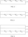
- FIG. 3 illustrates a cross-sectional view of a first portion of a bumpless superconductor device in its early stages of fabrication in accordance with a first methodology.
- a first substrate 100 is provided that includes a plurality of conductive contact pads 102 spaced apart from one another across a top surface of the first substrate 100.
- the first substrate can be formed of silicon or other structural material.
- the plurality of conductive contact pads 102 can be coupled to underlying devices in the first substrate 100 via conductive contacts (not shown) and/or conductive lines (not shown) within the first substrate 100.
- the plurality of conductive contact pads 102 can be formed by a photoresist patterning and contact material fill deposition processes. The photoresist can be stripped away or lifted off to form the plurality of conductive contact pads 102.
- a dielectric layer 104 is formed over the first substrate 100.
- Any suitable technique for forming the dielectric layer 104 may be employed such as Low Pressure Chemical Vapor Deposition (LPCVD), Plasma Enhanced Chemical Vapor Deposition (PECVD), High Density Plasma Chemical Vapor Deposition (HDPCVD), sputtering or spin-on techniques to a thickness suitable for providing an interconnect layer.
- the dielectric layer 104 can be a spin-on thermally curable polymer dielectric or other dielectric material that can provide both bonding properties and electrical isolation properties.
- a second substrate 106 is disposed over the dielectric layer 104 and aligned with the first substrate 100.
- the structure of FIG. 5 undergoes an oven baking process or other thermal process to cure the dielectric material layer 104 and bond the second substrate 106 to the first substrate 100.
- a photoresist material layer 107 has been applied to cover the structure of FIG. 5 and patterned and developed to expose via openings 108 in the photoresist material layer 107 in accordance with a via pattern.
- the photoresist material layer 107 can have a thickness that varies in correspondence with the wavelength of radiation used to pattern the photoresist material layer 107.
- the photoresist material layer 107 may be formed over the second substrate 106 via spin-coating or spin casting deposition techniques, selectively irradiated (e.g., via deep ultraviolet (DUV) irradiation) and developed to form the via openings 108.
- DUV deep ultraviolet
- FIG. 6 also illustrates performing of an etch 200 (e.g., anisotropic reactive ion etching (RIE)) on the second substrate 106 to form through substrate via (TSV) openings 110 ( FIG. 7 ) in the second substrate 106 based on the via pattern in the photoresist material layer 107.
- the etch step 200 can be a dry etch and employ an etchant which selectively etches the underlying second substrate 106 at a faster rate than the overlying photoresist material layer 107, and the underlying dielectric layer 104.
- the second substrate 106 may be anisotropically etched with a plasma gas(es), herein carbon tetrafloride (CF 4 ) containing fluorine ions, in a commercially available etcher, such as a parallel plate RIE apparatus or, alternatively, an electron cyclotron resonance (ECR) plasma reactor to replicate the mask pattern of the patterned of the photoresist material layer 107 to thereby create the TSV openings 110.
- a plasma gas(es) herein carbon tetrafloride (CF 4 ) containing fluorine ions
- CF 4 carbon tetrafloride
- ECR electron cyclotron resonance
- FIG. 7 also illustrates performing of a second etch 210 to form extended via openings 112 ( FIG. 8 ) through the dielectric layer 104 to the first substrate 100 based on the TSV pattern in the second substrate 106.
- the etch step 210 can be a dry etch and employ an etchant which selectively etches the underlying dielectric layer 104 at a faster rate than the overlying second substrate 106, and the underlying first substrate 100.
- the second etch 210 can be an oxygen plasma etch to form the extended via openings 112 with each respective extended opening being aligned with a respective conductive contact pad of the plurality of conductive contact pads 102, as illustrated in FIG. 8 .
- the structure then undergoes a contact material fill to deposit a superconducting material, such as aluminum, into the extended via openings 112 to form a plurality of superconducting contacts 114 ( FIG. 9 ) that extend from a top surface of the second substrate 106 to respective contact pads of the plurality of contact pads 102.
- a dielectric liner can be deposited to line or fill the extended via openings 112 prior to formation of the plurality of superconducting contacts 114.
- the contact material fill can be deposited employing a standard contact material deposition. Following deposition of the contact material fill, the contact material can be polished via chemical mechanical polishing (CMP) down to the surface level of the second substrate 106.
- CMP chemical mechanical polishing
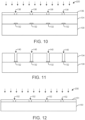
- FIG. 10 illustrates a cross-sectional view of a first portion of a bumpless superconductor device in its early stages of fabrication in accordance with a second methodology.
- a first substrate 130 is provided that includes a plurality of conductive contact pads 132 spaced apart from one another across a top surface of the first substrate 130.
- the first substrate 130 can be formed of silicon or other structural material.
- the plurality of conductive contact pads 132 can be coupled to underlying devices in the first substrate 130 via conductive contacts (not shown) and/or conductive lines (not shown) within the first substrate 130.
- the plurality of conductive contact pads 132 can be formed by photoresist patterning and contact material fill deposition processes. The photoresist can be stripped away or lifted off to form the plurality of conductive contact pads 132.
- a dielectric layer 134 is formed over the first substrate 130. Any suitable technique for forming the dielectric layer 134 may be employed such as Low Pressure Chemical Vapor Deposition (LPCVD), Plasma Enhanced Chemical Vapor Deposition (PECVD), High Density Plasma Chemical Vapor Deposition (HDPCVD), sputtering or spin-on techniques to a thickness suitable for providing an interconnect layer.
- the dielectric layer 134 can be a spin-on thermally curable polymer dielectric or other dielectric material that can provide both bonding properties and electrical isolation properties. This polymer can also be photoimageable meaning a separate photoresist patterning step is not necessary.
- a material like SU-8 or certain polyimides act as both structural dielectric and are photoimageable.
- a patterned photoresist material layer 136 has been applied to cover the structure of FIG. 10 , and patterned and developed to expose via openings 138 in the photoresist material layer 136 in accordance with a via pattern.
- the photoresist material layer 136 can have a thickness that varies in correspondence with the wavelength of radiation used to pattern the photoresist material layer 136.
- the photoresist material layer 36 may be formed over the dielectric layer via spin-coating or spin casting deposition techniques, selectively irradiated (e.g., via deep ultraviolet (DUV) irradiation) and developed to form the via openings 138.
- DUV deep ultraviolet
- FIG. 10 also illustrates performing of an etch 220 (e.g., anisotropic reactive ion etching (RIE)) on the dielectric layer 134 to form extended via openings 140 ( FIG. 11 ) to the first substrate 130 based on the via pattern in the photoresist material layer 136.
- the etch step 220 can be a dry etch and employ an etchant which selectively etches the underlying dielectric layer 134 at a faster rate than the overlying photoresist layer 136.
- the etch 220 can be an oxygen plasma etch to form the extended via openings 140 with each respective extended via opening 140 being aligned with a respective conductive contact pad of the plurality of conductive contact pads 132, as illustrated in FIG. 11 .
- a second substrate 150 is provided.
- a photoresist material layer 151 has been applied, to cover the structure of FIG. 12 , and patterned and developed to expose openings 152 in the photoresist material layer 151 in accordance with a via pattern.
- the photoresist material layer 151 can have a thickness that varies in correspondence with the wavelength of radiation used to pattern the photoresist material layer 151.
- the photoresist material layer 151 may be formed over the second substrate 150 via spin-coating or spin casting deposition techniques, selectively irradiated (e.g., via deep ultraviolet (DUV) irradiation) and developed to form the via openings 152.
- DUV deep ultraviolet
- FIG. 12 also illustrates performing of an etch 230 (e.g., anisotropic reactive ion etching (RIE)) on the second substrate 150 to form through substrate via (TSV) openings 154 ( FIG. 13 ) in the second substrate 150 based on the via pattern in the photoresist material layer 151.
- the etch step 230 can be a dry etch and employ an etchant which selectively etches the second substrate 150.
- the second substrate 150 may be anisotropically etched with a plasma gas(es), herein carbon tetrafloride (CF 4 ) containing fluorine ions, in a commercially available etcher, such as a parallel plate RIE apparatus or, alternatively, an electron cyclotron resonance (ECR) plasma reactor to replicate the mask pattern of the patterned of the photoresist material layer 151 to thereby create the TSV openings 154 ( FIG. 13 ).
- a plasma gas(es) herein carbon tetrafloride (CF 4 ) containing fluorine ions
- CF 4 carbon tetrafloride
- ECR electron cyclotron resonance
- the second substrate 150 is disposed over the dielectric layer 134 with the TSV openings 154 of the second substrate 150 being aligned with the extended via openings 140 of the dielectric layer 134.
- the structure of FIG. 14 undergoes an oven baking process or other thermal process to cure the dielectric material layer 134 and bond the second substrate 150 to the first substrate 130.
- the structure then undergoes a contact material fill to deposit a superconducting material, such as aluminum, into the TSV openings 150 and the extended via openings 140 to form a plurality of superconducting contacts 156 ( FIG. 15 ).
- a dielectric liner can be deposited to line or fill the openings 150 and 140 prior to formation of the plurality of superconducting contacts 156.
- the contact material fill can be deposited employing a standard contact material deposition. Following deposition of the contact material fill, the superconducting material is polished via chemical mechanical polishing (CMP) down to the surface level of the second substrate to provide the resultant structure of FIG. 15 .
- CMP chemical mechanical polishing
- the performing of the etch 230 to form the through substrate via (TSV) openings 154 in the second substrate 150 occurs after the second substrate 150 is bonded to the dielectric layer 134.
- the TSV openings 154 are aligned with the extended via openings 140 in the dielectric layer 134.
- This type of methodology allows for cavities between the bottom and top substrate which would keep sensitive structures (e.g., Qubits) from being covered by dielectric in the final stack.
- top substrate IC fabrication proceeds on the bonded substrate pair until final TSV drilling. This process could also facilitate the formation of hermetically sealed cavities using a photo imageable dielectric to form openings in the interchip dielectric. After bonding, vias could be formed to open to these cavities followed by metal sputtering in vacuum to close the vias. Additionally, the present examples illustrate the bonding of two substrates, but the methodologies could be extended to a structure with three or more substrates.
- overlay For purposes of simplification of explanation the terms “overlay”, “overlaying”, “overlying”, “underlay” and “underlying” (and derivatives) are employed throughout this disclosure to denote a relative position of two adjacent surfaces in a selected orientation. Additionally, the terms “top” and “bottom” employed throughout this disclosure denote opposing surfaces in the selected orientation. Similarly, the terms “upper” and “lower” denote relative positions in the selected orientation are for purposes of illustration. In fact, the examples used throughout this disclosure denote one selected orientation. In the described examples, however, the selected orientation is arbitrary and other orientations are possible (e.g., upside down, rotated by 90 degrees, etc.) within the scope of the present disclosure.
Landscapes
- Engineering & Computer Science (AREA)
- Manufacturing & Machinery (AREA)
- Internal Circuitry In Semiconductor Integrated Circuit Devices (AREA)
- Superconductor Devices And Manufacturing Methods Thereof (AREA)
Abstract
Description
- This application claims priority from
U.S. Patent Application Serial No. 16/858812, filed 27 April 2020 - The present disclosure relates generally to integrated circuits, and more particularly to a bumpless superconductor device.
- High density three-dimensional (3D) chip integration techniques generally involve the bonding of two separate substrates/chips using some variation of bump bonding. Bumps are raised metallic pillars/spheres on the order of 25-200um in diameter and 10-200um tall formed on the surface of chips/substrates. Bump bonding requires that the substrates to be joined are "bumped" with a suitable joining metal (SnPb, SnAg, SnCu, In, etc.). Substrate bumping involves the patterning and deposition of under bump metallization layers (ex. Ti, TiW, Cr, Pd, Ni, etc.) which act as adhesion promoters and/or diffusion barriers followed by plating of the aforementioned joining metal. Once "bumped" the substrates or chips are joined by precisely aligning the bumps and applying either force, temperature, ultrasonic power, or a combination thereof to form conducting metallic joints between the two chips. Subsequent to this joining process it is standard for a thermoset polymer material (typically epoxy based) called an underfill to be dispensed between the two joined layers which acts as a stress buffer and isolates the bumps from the ambient environment.
- The drive for lower power, lower latency, higher interconnect density requires that the chip-to-chip connections become smaller in diameter and tighter in pitch. State of the art volume production chip bumping used in HBM (high bandwidth memory) currently utilizes Cu-pillar microbumps on the order of 25um diameter and bump pitches of 55um. Beyond this and indeed even at this stage the cost of this packaging integration is driving the use of this technology only for the high-end of the GPU, NPU, CPU markets among others. At these pitches and diameters, it becomes difficult to maintain bump yield and bonding yield as alignment and planarity of the bonding process needs to be precisely controlled in order to insure that all bumps are joined. Generally flip chip bonding of this sort is not reworkable. Additionally, a side effect of shrinking bump diameters is a decrease in bump heights and therefore decrease in chip-to-chip spacing as there are limitation to the aspect ratio of plated pillars. This increases the stress on the bumps which is a function of stand-off height. It also places additional constraints on the underfill materials and underfill dispense process as highly engineered low viscosity materials needs to be developed to fill these tight gaps and very precise liquid dispense tools to ensure that underfill dispense volumes are consistent.
- In one example, an integrated circuit is provided that comprises a first substrate having a plurality of conductive contact pads spaced apart from one another on a surface of the first substrate, a dielectric layer overlying the first substrate and the plurality of conductive contact pads, and a second substrate overlying the dielectric layer. A plurality of superconducting contacts extend through the second substrate and the dielectric layer to the first substrate, wherein each superconducting contact of the plurality of superconducting contacts is aligned with and in contact with a respective conductive contact pad of the plurality of conductive contact pads.
- In another example, a method of forming a superconductor device is disclosed. The method comprises providing a first substrate having a plurality of conductive contact pads spaced apart from one another on a surface of the first substrate, disposing a dielectric layer over the first substrate and the plurality of conductive contact pads, and disposing a second substrate over the dielectric layer. A plurality of vias are formed from a top surface of the second substrate, through the second substrate and the dielectric layer to the first substrate with each via extending to and being aligned with a respective conductive contact pad of the plurality of conductive contact pads. The method further comprises performing a contact material fill to fill the plurality of vias with superconducting material and form a plurality of superconducting contacts extending through the second substrate and the dielectric layer to the first substrate, wherein each superconducting contact of the plurality of superconducting contacts is aligned with and in contact with a respective conductive contact pad of the plurality of conductive contact pads.
- In yet a further example, a method of forming an integrated circuit is disclosed. The method comprises providing a first substrate having a plurality of conductive contact pads spaced apart from one another on a surface of the first substrate, disposing a dielectric layer over the first substrate and the plurality of conductive contact pads, and performing a first etch on the dielectric layer to provide extended via openings through the dielectric layer to the first substrate with each extended via openings being aligned with a respective conductive contact pad of the plurality of conductive contact pads. The method further comprises performing a second etch on the second substrate to form a plurality of through substrate via (TSV) openings in the second substrate, and disposing the second substrate over the dielectric layer with the plurality of TSV openings being aligned with the plurality of extended via openings to form a plurality of vias from a top surface of the second substrate, through the second substrate and the dielectric layer to the first substrate with each via extending to and being aligned with a respective conductive contact pad of the plurality of conductive contact pads. The method also comprises performing a contact material fill to fill the plurality of vias with superconducting material and form a plurality of superconducting contacts extending through the second substrate and the dielectric layer to the first substrate, wherein each superconducting contact of the plurality of superconducting contacts is aligned with and in contact with a respective conductive contact pad of the plurality of conductive contact pads.
-
-
FIG. 1 illustrates cross-sectional view of a portion of an example integrated circuit. -
FIG. 2 illustrates cross-sectional view of a portion of another example integrated circuit -
FIG. 3 illustrates a cross-sectional view of a first portion of a bumpless superconductor device in its early stages of fabrication in accordance with a first methodology. -
FIG. 3 illustrates a cross-sectional view of a first portion of a bumpless superconductor device in its early stages of fabrication in accordance with a first methodology. -
FIG. 4 illustrates a cross-sectional view of the structure ofFIG. 3 after deposition of an overlying dielectric layer. -
FIG. 5 illustrates a cross-sectional view of the structure ofFIG. 4 after disposing a second substrate over the dielectric layer. -
FIG. 6 illustrates a cross-sectional view of the structure ofFIG. 5 after deposition and patterning of a photoresist material layer and while undergoing a first etch process. -
FIG. 7 illustrates a cross-sectional view of the structure ofFIG. 6 while undergoing a second etch process. -
FIG. 8 illustrates a cross-sectional view of the structure ofFIG. 7 after undergoing the second etch process. -
FIG. 9 illustrates a cross-sectional view of the structure ofFIG. 8 after a superconducting material fill process. -
FIG. 10 illustrates a cross-sectional view of a first portion of a bumpless superconductor device in its early stages of fabrication in accordance with a second methodology, and while undergoing a first etch process. -
FIG. 11 illustrates a cross-sectional view of the structure ofFIG. 10 after undergoing the first etch process. -
FIG. 12 illustrates a cross-sectional view of a second substrate undergoing a second etch process. -
FIG. 13 illustrates a cross-sectional view of the structure ofFIG. 12 of the second substrate after undergoing the second etch process. -
FIG. 14 illustrates a cross-sectional view of the structure ofFIG. 11 after disposing of the second substrate ofFIG. 13 over the structure ofFIG. 11 . -
FIG. 15 illustrates a cross-sectional view of the structure ofFIG. 14 after a superconducting material fill process. - The present disclosure describes a bumpless superconductor device and methods of making a bumpless superconductor device. In one example, two substrates are joined together via a dielectric material. As an example, a spin-on thermally curable polymer dielectric can be deposited on a first substrate (e.g., formed of silicon, glass, compound semiconductors, or a variety of other semiconductor materials). A second substrate (e.g., formed of silicon, glass, compound semiconductors, or a variety of other semiconductor materials) can then be aligned and bonded to this substrate face up or face down. The application of heat during bonding cures the polymer resulting in the substrates being joined. A substrate can be either in chip or wafer format. Subsequently, high aspect ratio vias (e.g., through substrate vias (TSVs)) are etched through the top substrate using, for example, masked plasma etching (e.g., by a Bosch process). Once the vias reach the dielectric layer between the two substrates, a different plasma gas mixture can be used to etch through this polymer or other dielectric (using the TSVs as an etch mask) down to respective metal pads on the bottom substrate. In this way, very dense and very small diameter vias can be formed. A dielectric liner can be deposited via PECVD or ALD followed by sputtering a conductive material to line or fill the vias. A variation of this process has the vias pre-etched in the second substrate and the dielectric layer and aligned to provide mating vias with the dielectric prior to or after the bonding process.
- The present disclosure provides an alternative to bump bonding techniques of high density chip integration, and also reduces the burden of precise planarity control during the substrate bonding process. This technique also allows for the use of interchip metallization other than low temperature melting metals/alloys to include any sputterable material (e.g., high temperature superconducting metals). In addition, it reduces the complexity and engineering of the underfill formulation and dispensing process.
-
FIG. 1 illustrates a schematic cross-sectional view of a portion of an examplebumpless superconductor device 10. Afirst substrate 12 includes a plurality ofconductive contact pads 20 spaced apart from one another across a top surface of thefirst substrate 12. The plurality ofconductive contact pads 20 can be coupled to underlying devices in thefirst substrate 12 via conductive contacts (not shown) and/or conductive lines (not shown) within thefirst substrate 12. Asecond substrate 16 is aligned and bonded to thefirst substrate 12 by adielectric layer 14. A plurality ofsuperconducting contacts 18 extend from a top surface of thesecond substrate 16 through thesecond substrate 16, and thedielectric layer 14 to respective contact pads of the plurality ofcontact pads 20 disposed on the top surface of thefirst substrate 12. A dielectric liner can be deposited to line or fill the vias prior to formation of the plurality ofsuperconducting contacts 18. - The first and
second substrates superconducting contacts 18 can be formed of a superconducting material, such as aluminum, niobium, niobium titanium nitride, niobium nitride or some other superconducting material, compound or alloy. Thedielectric layer 14 can be a spin-on thermally curable polymer dielectric or other dielectric material that can provide both bonding of thefirst substrate 12 and thesecond substrate 16 and electrical isolation of the plurality ofsuperconducting contacts 18. Alternatively, a bonding agent can be employed to bond thefirst substrate 12 and thesecond substrate 16 to thedielectric layer 14. -
FIG. 2 illustrates schematic cross-sectional view of a portion of an example bumpless superconductor device 50 with superconducting elements. Afirst substrate 52 includes a plurality ofconductive contact pads 60 spaced apart from one another across a top surface of thefirst substrate 52. Each of the plurality ofconductive contact pads 60 are coupled to arespective qubit device 62 disposed within thefirst substrate 52. Although illustrated as thequbit devices 62 and theconductive contact pads 60 being directly coupled together, the coupling could occur via conductive contacts and/or conductive lines within thefirst substrate 52. Asecond substrate 56 is aligned and bonded to thefirst substrate 52 by adielectric layer 54. A plurality ofsuperconducting contacts 58 extend from a top surface of thesecond substrate 56 through thesecond substrate 56 and thedielectric layer 54 to respective conductive contact pads of the plurality ofconductive contact pads 60 disposed on the top surface of thefirst substrate 52. - A first end of each
respective superconducting contact 58 is coupled to arespective resonator 64 on the top surface of thesecond substrate 56, and a second end of eachrespective superconducting contact 58 is coupled to a respectiveconductive contact pad 60, and thus arespective qubit device 62. Theresonators 64 can be printed or etched into the top surface of thesecond substrate 56. Similar toFIG. 1 , the first andsecond substrates superconducting contacts 58 can be formed of a superconducting material, such as aluminum, niobium, or some other superconducting material, and thedielectric layer 54 can be a spin-on thermally curable polymer dielectric or other dielectric material. - Turning now to
FIGS. 3-15 , fabrication is discussed in connection with formation of the bumpless superconductor device ofFIG. 1 . A first methodology is illustrated inFIGS. 3-9 in which vias are formed through a top substrate and through a dielectric layer after bonding of two substrate together via the dielectric layer. A second methodology is illustrated inFIGS. 10-15 in which vias are formed through a top substrate and a dielectric layer separately, and the top substrate is disposed over the dielectric layer are aligned with the vias of the top substrate being aligned with respective vias of the dielectric layer followed by the bonding of the top and bottom substrates together by through the dielectric layer. -
FIG. 3 illustrates a cross-sectional view of a first portion of a bumpless superconductor device in its early stages of fabrication in accordance with a first methodology. Afirst substrate 100 is provided that includes a plurality ofconductive contact pads 102 spaced apart from one another across a top surface of thefirst substrate 100. The first substrate can be formed of silicon or other structural material. The plurality ofconductive contact pads 102 can be coupled to underlying devices in thefirst substrate 100 via conductive contacts (not shown) and/or conductive lines (not shown) within thefirst substrate 100. The plurality ofconductive contact pads 102 can be formed by a photoresist patterning and contact material fill deposition processes. The photoresist can be stripped away or lifted off to form the plurality ofconductive contact pads 102. - As illustrated in
FIG. 4 , adielectric layer 104 is formed over thefirst substrate 100. Any suitable technique for forming thedielectric layer 104 may be employed such as Low Pressure Chemical Vapor Deposition (LPCVD), Plasma Enhanced Chemical Vapor Deposition (PECVD), High Density Plasma Chemical Vapor Deposition (HDPCVD), sputtering or spin-on techniques to a thickness suitable for providing an interconnect layer. Thedielectric layer 104 can be a spin-on thermally curable polymer dielectric or other dielectric material that can provide both bonding properties and electrical isolation properties. Next, as illustrated inFIG. 5 , asecond substrate 106 is disposed over thedielectric layer 104 and aligned with thefirst substrate 100. The structure ofFIG. 5 undergoes an oven baking process or other thermal process to cure thedielectric material layer 104 and bond thesecond substrate 106 to thefirst substrate 100. - As illustrated in
FIG. 6 , aphotoresist material layer 107 has been applied to cover the structure ofFIG. 5 and patterned and developed to expose viaopenings 108 in thephotoresist material layer 107 in accordance with a via pattern. Thephotoresist material layer 107 can have a thickness that varies in correspondence with the wavelength of radiation used to pattern thephotoresist material layer 107. Thephotoresist material layer 107 may be formed over thesecond substrate 106 via spin-coating or spin casting deposition techniques, selectively irradiated (e.g., via deep ultraviolet (DUV) irradiation) and developed to form the viaopenings 108. -
FIG. 6 also illustrates performing of an etch 200 (e.g., anisotropic reactive ion etching (RIE)) on thesecond substrate 106 to form through substrate via (TSV) openings 110 (FIG. 7 ) in thesecond substrate 106 based on the via pattern in thephotoresist material layer 107. Theetch step 200 can be a dry etch and employ an etchant which selectively etches the underlyingsecond substrate 106 at a faster rate than the overlyingphotoresist material layer 107, and theunderlying dielectric layer 104. For example, thesecond substrate 106 may be anisotropically etched with a plasma gas(es), herein carbon tetrafloride (CF4) containing fluorine ions, in a commercially available etcher, such as a parallel plate RIE apparatus or, alternatively, an electron cyclotron resonance (ECR) plasma reactor to replicate the mask pattern of the patterned of thephotoresist material layer 107 to thereby create theTSV openings 110. Thephotoresist material layer 107 is thereafter removed using an oxygen based plasma and wet cleaned to remove organic residues. As a result, theTSV openings 110 extend to the surface of thedielectric layer 104. -
FIG. 7 also illustrates performing of asecond etch 210 to form extended via openings 112 (FIG. 8 ) through thedielectric layer 104 to thefirst substrate 100 based on the TSV pattern in thesecond substrate 106. Theetch step 210 can be a dry etch and employ an etchant which selectively etches theunderlying dielectric layer 104 at a faster rate than the overlyingsecond substrate 106, and the underlyingfirst substrate 100. For example, thesecond etch 210 can be an oxygen plasma etch to form the extended viaopenings 112 with each respective extended opening being aligned with a respective conductive contact pad of the plurality ofconductive contact pads 102, as illustrated inFIG. 8 . - Next, the structure then undergoes a contact material fill to deposit a superconducting material, such as aluminum, into the extended via
openings 112 to form a plurality of superconducting contacts 114 (FIG. 9 ) that extend from a top surface of thesecond substrate 106 to respective contact pads of the plurality ofcontact pads 102. A dielectric liner can be deposited to line or fill the extended viaopenings 112 prior to formation of the plurality ofsuperconducting contacts 114. The contact material fill can be deposited employing a standard contact material deposition. Following deposition of the contact material fill, the contact material can be polished via chemical mechanical polishing (CMP) down to the surface level of thesecond substrate 106. The final resultant structure is illustrated inFIG. 9 . -
FIG. 10 illustrates a cross-sectional view of a first portion of a bumpless superconductor device in its early stages of fabrication in accordance with a second methodology. Afirst substrate 130 is provided that includes a plurality ofconductive contact pads 132 spaced apart from one another across a top surface of thefirst substrate 130. Thefirst substrate 130 can be formed of silicon or other structural material. The plurality ofconductive contact pads 132 can be coupled to underlying devices in thefirst substrate 130 via conductive contacts (not shown) and/or conductive lines (not shown) within thefirst substrate 130. The plurality ofconductive contact pads 132 can be formed by photoresist patterning and contact material fill deposition processes. The photoresist can be stripped away or lifted off to form the plurality ofconductive contact pads 132. - A
dielectric layer 134 is formed over thefirst substrate 130. Any suitable technique for forming thedielectric layer 134 may be employed such as Low Pressure Chemical Vapor Deposition (LPCVD), Plasma Enhanced Chemical Vapor Deposition (PECVD), High Density Plasma Chemical Vapor Deposition (HDPCVD), sputtering or spin-on techniques to a thickness suitable for providing an interconnect layer. Thedielectric layer 134 can be a spin-on thermally curable polymer dielectric or other dielectric material that can provide both bonding properties and electrical isolation properties. This polymer can also be photoimageable meaning a separate photoresist patterning step is not necessary. A material like SU-8 or certain polyimides act as both structural dielectric and are photoimageable. - A patterned
photoresist material layer 136 has been applied to cover the structure ofFIG. 10 , and patterned and developed to expose viaopenings 138 in thephotoresist material layer 136 in accordance with a via pattern. Thephotoresist material layer 136 can have a thickness that varies in correspondence with the wavelength of radiation used to pattern thephotoresist material layer 136. The photoresist material layer 36 may be formed over the dielectric layer via spin-coating or spin casting deposition techniques, selectively irradiated (e.g., via deep ultraviolet (DUV) irradiation) and developed to form the viaopenings 138. -
FIG. 10 also illustrates performing of an etch 220 (e.g., anisotropic reactive ion etching (RIE)) on thedielectric layer 134 to form extended via openings 140 (FIG. 11 ) to thefirst substrate 130 based on the via pattern in thephotoresist material layer 136. Theetch step 220 can be a dry etch and employ an etchant which selectively etches theunderlying dielectric layer 134 at a faster rate than the overlyingphotoresist layer 136. For example, theetch 220 can be an oxygen plasma etch to form the extended viaopenings 140 with each respective extended viaopening 140 being aligned with a respective conductive contact pad of the plurality ofconductive contact pads 132, as illustrated inFIG. 11 . - Next, as illustrated in
FIG. 12 , asecond substrate 150 is provided. As illustrated inFIG. 12 , aphotoresist material layer 151 has been applied, to cover the structure ofFIG. 12 , and patterned and developed to exposeopenings 152 in thephotoresist material layer 151 in accordance with a via pattern. Thephotoresist material layer 151 can have a thickness that varies in correspondence with the wavelength of radiation used to pattern thephotoresist material layer 151. Thephotoresist material layer 151 may be formed over thesecond substrate 150 via spin-coating or spin casting deposition techniques, selectively irradiated (e.g., via deep ultraviolet (DUV) irradiation) and developed to form the viaopenings 152. -
FIG. 12 also illustrates performing of an etch 230 (e.g., anisotropic reactive ion etching (RIE)) on thesecond substrate 150 to form through substrate via (TSV) openings 154 (FIG. 13 ) in thesecond substrate 150 based on the via pattern in thephotoresist material layer 151. Theetch step 230 can be a dry etch and employ an etchant which selectively etches thesecond substrate 150. For example, thesecond substrate 150 may be anisotropically etched with a plasma gas(es), herein carbon tetrafloride (CF4) containing fluorine ions, in a commercially available etcher, such as a parallel plate RIE apparatus or, alternatively, an electron cyclotron resonance (ECR) plasma reactor to replicate the mask pattern of the patterned of thephotoresist material layer 151 to thereby create the TSV openings 154 (FIG. 13 ). Thephotoresist material layer 151 is thereafter removed using an oxygen based plasma and wet cleaned to remove organic residues to provide the resultant structure ofFIG. 13 . - As illustrated in
FIG. 14 , thesecond substrate 150 is disposed over thedielectric layer 134 with theTSV openings 154 of thesecond substrate 150 being aligned with the extended viaopenings 140 of thedielectric layer 134. The structure ofFIG. 14 undergoes an oven baking process or other thermal process to cure thedielectric material layer 134 and bond thesecond substrate 150 to thefirst substrate 130. Next, the structure then undergoes a contact material fill to deposit a superconducting material, such as aluminum, into theTSV openings 150 and the extended viaopenings 140 to form a plurality of superconducting contacts 156 (FIG. 15 ). A dielectric liner can be deposited to line or fill theopenings superconducting contacts 156. The contact material fill can be deposited employing a standard contact material deposition. Following deposition of the contact material fill, the superconducting material is polished via chemical mechanical polishing (CMP) down to the surface level of the second substrate to provide the resultant structure ofFIG. 15 . - There are many potential variations to the above described process flow with various types of chips being integrated. For example, in an alternate method, the performing of the
etch 230 to form the through substrate via (TSV)openings 154 in thesecond substrate 150 occurs after thesecond substrate 150 is bonded to thedielectric layer 134. TheTSV openings 154 are aligned with the extended viaopenings 140 in thedielectric layer 134. This type of methodology allows for cavities between the bottom and top substrate which would keep sensitive structures (e.g., Qubits) from being covered by dielectric in the final stack. - As another example, it's possible to imagine bonding two substrates wherein only the bottom substrate has completed IC fabrication. The top substrate being bare requires no precise alignment to the lower layer during bonding since there are no pads to align to. Once bonded the use of xray or IR imaging can be used to align fiducials on the top side of the top substrate to align precisely with pads on the bottom substrate. Top substrate IC fabrication proceeds on the bonded substrate pair until final TSV drilling. This process could also facilitate the formation of hermetically sealed cavities using a photo imageable dielectric to form openings in the interchip dielectric. After bonding, vias could be formed to open to these cavities followed by metal sputtering in vacuum to close the vias. Additionally, the present examples illustrate the bonding of two substrates, but the methodologies could be extended to a structure with three or more substrates.
- For purposes of simplification of explanation the terms "overlay", "overlaying", "overlying", "underlay" and "underlying" (and derivatives) are employed throughout this disclosure to denote a relative position of two adjacent surfaces in a selected orientation. Additionally, the terms "top" and "bottom" employed throughout this disclosure denote opposing surfaces in the selected orientation. Similarly, the terms "upper" and "lower" denote relative positions in the selected orientation are for purposes of illustration. In fact, the examples used throughout this disclosure denote one selected orientation. In the described examples, however, the selected orientation is arbitrary and other orientations are possible (e.g., upside down, rotated by 90 degrees, etc.) within the scope of the present disclosure.
- Described above are examples of the subject disclosure. It is, of course, not possible to describe every conceivable combination of components or methodologies for purposes of describing the subject disclosure, but one of ordinary skill in the art may recognize that many further combinations and permutations of the subject disclosure are possible. Accordingly, the subject disclosure is intended to embrace all such alterations, modifications and variations that fall within the spirit and scope of the appended claims. In addition, where the disclosure or claims recite "a," "an," "a first," or "another" element, or the equivalent thereof, it should be interpreted to include one or more than one such element, neither requiring nor excluding two or more such elements. Furthermore, to the extent that the term "includes" is used in either the detailed description or the claims, such term is intended to be inclusive in a manner similar to the term "comprising" as "comprising" is interpreted when employed as a transitional word in a claim. Finally, the term "based on" is interpreted to mean at least based in part.
- The present disclosure provides the following Clauses:
- Clause 1. An integrated circuit comprising:
- a first substrate having a plurality of conductive contact pads spaced apart from one another on a surface of the first substrate;
- a dielectric layer overlying the first substrate and the plurality of conductive contact pads;
- a second substrate overlying the dielectric layer; and
- a plurality of superconducting contacts extending through the second substrate and the dielectric layer to the first substrate, wherein each superconducting contact of the plurality of superconducting contacts is aligned with and in contact with a respective conductive contact pad of the plurality of conductive contact pads.
- Clause 2. The circuit of Clause 1, wherein the dielectric layer is a thermally curable polymer.
- Clause 3. The circuit of Clause 1, wherein the first substrate is formed of one of silicon, glass, or compound semiconductors and the second substrate is formed of one of silicon, glass, or compound semiconductors.
- Clause 4. The circuit of Clause 1, wherein the plurality of superconducting contacts are formed of one of aluminum, niobium, niobium titanium nitride, and niobium nitride.
- Clause 5. The circuit of Clause 1, further comprises a plurality of qubits disposed within the first substrate, such that each of the plurality of conductive contact pads are coupled to a respective qubit of the plurality of qubits.
- Clause 6. The circuit of Clause 5, further comprising a plurality of resonators disposed on the second substrate, such that each of the plurality of superconducting contacts are coupled to a respective resonator of the plurality of resonators, and each respective resonator of the plurality of resonators is coupled to a respective qubit of the plurality of qubits.
- Clause 7. A method of forming an integrated circuit, the method comprising:
- providing a first substrate having a plurality of conductive contact pads spaced apart from one another on a surface of the first substrate;
- disposing a dielectric layer over the first substrate and the plurality of conductive contact pads;
- disposing a second substrate over the dielectric layer;
- forming a plurality of vias from a top surface of the second substrate, through the second substrate and the dielectric layer to the first substrate with each via extending to and being aligned with a respective conductive contact pad of the plurality of conductive contact pads; and
- performing a contact material fill to fill the plurality of vias with superconducting material and form a plurality of superconducting contacts extending through the second substrate and the dielectric layer to the first substrate, wherein each superconducting contact of the plurality of superconducting contacts is aligned with and in contact with a respective conductive contact pad of the plurality of conductive contact pads.
- Clause 8. The method of Clause 7, further comprising heating the dielectric layer to bond the second substrate to the first substrate, wherein the dielectric layer is a thermally curable polymer.
- Clause 9. The method of Clause 7, wherein the forming a plurality of vias comprises performing a first etch on the second substrate to form a plurality of through substrate via (TSV) openings in the second substrate, and performing a second etch on the second substrate and the dielectric layer to provide extended openings through the dielectric layer to the first substrate based on a mask pattern formed by the plurality of TSV openings in the second substrate.
-
Clause 10. The method of Clause 7, wherein the first substrate and the second substrate are both formed of one of silicon, glass, or compound semiconductors. - Clause 11. The method of Clause 7, wherein the plurality of superconducting contacts are formed of one of aluminum, niobium, niobium titanium nitride, and niobium nitride.
-
Clause 12. The method of Clause 7, further comprises fabricating a plurality of qubits disposed within the first substrate, such that each of the plurality of conductive contact pads are coupled to a respective qubit of the plurality of qubits. - Clause 13. The method of
Clause 12, further comprising fabricating a plurality of resonators disposed on the second substrate, such that each of the plurality of superconducting contacts are coupled to a respective resonator of the plurality of resonators, and each respective resonator of the plurality of resonators is coupled to a respective qubit of the plurality of qubits. -
Clause 14. The method of Clause 7, wherein the forming a plurality of vias comprises:- performing a first etch on the dielectric layer to provide extended via openings through the dielectric layer to the first substrate;
- performing a second etch on the second substrate, prior to the second substrate being disposed over the dielectric layer, to form a plurality of through substrate via (TSV) openings in the second substrate; and
- wherein the disposing the second substrate over the dielectric layer comprises disposing the second substrate over the dielectric layer with the plurality of TSV openings being aligned with the plurality of extended via openings to form a plurality of vias from a top surface of the second substrate, through the second substrate and the dielectric layer to the first substrate with each via extending to and being aligned with a respective conductive contact pad of the plurality of conductive contact pads.
- Clause 15. A method of forming an integrated circuit, the method comprising:
- providing a first substrate having a plurality of conductive contact pads spaced apart from one another on a surface of the first substrate;
- disposing a dielectric layer over the first substrate and the plurality of conductive contact pads;
- performing a first etch on the dielectric layer to provide extended via openings through the dielectric layer to the first substrate with each extended via openings being aligned with a respective conductive contact pad of the plurality of conductive contact pads;
- performing a second etch on a second substrate to form a plurality of through substrate via (TSV) openings in the second substrate;
- disposing the second substrate over the dielectric layer, wherein the second substrate is disposed over the dielectric layer one of before or after the second etch, the plurality of TSV openings being aligned with the plurality of extended via openings to form a plurality of vias from a top surface of the second substrate, through the second substrate and the dielectric layer to the first substrate with each via extending to and being aligned with a respective conductive contact pad of the plurality of conductive contact pads; and
- performing a contact material fill to fill the plurality of vias with superconducting material and form a plurality of superconducting contacts extending through the second substrate and the dielectric layer to the first substrate, wherein each superconducting contact of the plurality of superconducting contacts is aligned with and in contact with a respective conductive contact pad of the plurality of conductive contact pads.
-
Clause 16. The method of Clause 15, further comprising heating the dielectric layer to bond the second substrate to the first substrate, wherein the dielectric layer is a thermally curable polymer. - Clause 17. The method of Clause 15, wherein the first substrate and the second substrate are both formed of one of silicon, glass, or compound semiconductors.
-
Clause 18. The method of Clause 15, wherein the plurality of superconducting contacts are formed of one of aluminum, niobium, niobium titanium nitride, and niobium nitride. - Clause 19. The method of Clause 15, further comprises fabricating a plurality of qubits disposed within the first substrate, such that each of the plurality of conductive contact pads are coupled to a respective qubit of the plurality of qubits.
-
Clause 20. The method of Clause 19, further comprising fabricating a plurality of resonators disposed on the second substrate, such that each of the plurality of superconducting contacts are coupled to a respective resonator of the plurality of resonators, and each respective resonator of the plurality of resonators is coupled to a respective qubit of the plurality of qubits.
Claims (7)
- A method of forming an integrated circuit, the method comprising:providing a first substrate (130) having a plurality of conductive contact pads (132) spaced apart from one another on a surface of the first substrate (130);disposing a dielectric layer (134) over the first substrate (130) and the plurality of conductive contact pads (132);performing a first etch (220) on the dielectric layer to provide extended via openings (140) through the dielectric layer (134) to the first substrate (130) with each extended via opening being aligned with a respective conductive contact pad of the plurality of conductive contact pads (132);performing a second etch (230) on a second substrate (150) to form a plurality of through substrate via, TSV, openings (154) in the second substrate;disposing the second substrate (150) over the dielectric layer (134), wherein the second substrate (150) is disposed over the dielectric layer (134) one of before or after the second etch (230), the plurality of TSV openings (154) being aligned with the plurality of extended via openings (140) to form a plurality of vias from a top surface of the second substrate, through the second substrate (150) and the dielectric layer (134) to the first substrate (130) with each via extending to and being aligned with a respective conductive contact pad of the plurality of conductive contact pads (132); andperforming a contact material fill to fill the plurality of vias with superconducting material and form a plurality of superconducting contacts (156) extending through the second substrate (150) and the dielectric layer (134) to the first substrate (130), wherein each superconducting contact of the plurality of superconducting contacts (156) is aligned with and in contact with a respective conductive contact pad of the plurality of conductive contact pads (132).
- The method of claim 1, further comprising heating the dielectric layer (134) to bond the second substrate (150) to the first substrate (130), wherein the dielectric layer (134) is a thermally curable polymer.
- The method of claim 1, wherein the first substrate (130) and the second substrate (150) are both formed of one of silicon, glass, or compound semiconductors.
- The method of claim 1, wherein the plurality of superconducting contacts (156) are formed of one of aluminum, niobium, niobium titanium nitride, and niobium nitride.
- The method of claim 1, further comprising fabricating a plurality of qubits (62) disposed within the first substrate (130), such that each of the plurality of conductive contact pads (132) is coupled to a respective qubit of the plurality of qubits (62).
- The method of claim 5, further comprising fabricating a plurality of resonators (64) disposed on the second substrate (150), such that each of the plurality of superconducting contacts (156) is coupled to a respective resonator of the plurality of resonators (64), and each respective resonator of the plurality of resonators (64) is coupled to a respective qubit of the plurality of qubits (62).
- The method of claim 1, further comprising, prior to forming the plurality of superconducting contacts (156), depositing a dielectric liner to line or fill the extended via openings (140) and the TSV openings (154).
Applications Claiming Priority (3)
| Application Number | Priority Date | Filing Date | Title |
|---|---|---|---|
| US16/858,812 US11417819B2 (en) | 2020-04-27 | 2020-04-27 | Forming a bumpless superconductor device by bonding two substrates via a dielectric layer |
| PCT/US2021/024070 WO2021221834A1 (en) | 2020-04-27 | 2021-03-25 | Bumpless superconductor device |
| EP21720330.6A EP4143883B1 (en) | 2020-04-27 | 2021-03-25 | Bumpless superconductor device and method of fabricating the same |
Related Parent Applications (2)
| Application Number | Title | Priority Date | Filing Date |
|---|---|---|---|
| EP21720330.6A Division EP4143883B1 (en) | 2020-04-27 | 2021-03-25 | Bumpless superconductor device and method of fabricating the same |
| EP21720330.6A Division-Into EP4143883B1 (en) | 2020-04-27 | 2021-03-25 | Bumpless superconductor device and method of fabricating the same |
Publications (2)
| Publication Number | Publication Date |
|---|---|
| EP4207996A1 true EP4207996A1 (en) | 2023-07-05 |
| EP4207996B1 EP4207996B1 (en) | 2024-05-15 |
Family
ID=75588261
Family Applications (2)
| Application Number | Title | Priority Date | Filing Date |
|---|---|---|---|
| EP23151185.8A Active EP4207996B1 (en) | 2020-04-27 | 2021-03-25 | Method of forming bumpless superconductor device |
| EP21720330.6A Active EP4143883B1 (en) | 2020-04-27 | 2021-03-25 | Bumpless superconductor device and method of fabricating the same |
Family Applications After (1)
| Application Number | Title | Priority Date | Filing Date |
|---|---|---|---|
| EP21720330.6A Active EP4143883B1 (en) | 2020-04-27 | 2021-03-25 | Bumpless superconductor device and method of fabricating the same |
Country Status (6)
| Country | Link |
|---|---|
| US (2) | US11417819B2 (en) |
| EP (2) | EP4207996B1 (en) |
| KR (1) | KR102947134B1 (en) |
| CN (1) | CN115700068A (en) |
| AU (1) | AU2021263297A1 (en) |
| WO (1) | WO2021221834A1 (en) |
Families Citing this family (4)
| Publication number | Priority date | Publication date | Assignee | Title |
|---|---|---|---|---|
| FR3118022B1 (en) * | 2020-12-23 | 2023-02-10 | Commissariat Energie Atomique | Method for determining the position of the totally isolated regime of a spin qubit and method for manipulating at least one spin qubit |
| FI20215520A1 (en) * | 2021-05-04 | 2022-11-05 | Iqm Finland Oy | Superconducting vias in substrates |
| FR3128313A1 (en) * | 2021-10-14 | 2023-04-21 | Commissariat A L'energie Atomique Et Aux Energies Alternatives | Matrix of spin-qubit quantum dots |
| KR102923356B1 (en) * | 2024-11-06 | 2026-02-05 | 포항공과대학교 산학협력단 | Resonant circuit device including qubit and method for manufacturing the same |
Citations (4)
| Publication number | Priority date | Publication date | Assignee | Title |
|---|---|---|---|---|
| US20100244201A1 (en) * | 2009-03-25 | 2010-09-30 | Fujitsu Limited | Semiconductor device |
| US20150145094A1 (en) * | 2013-11-27 | 2015-05-28 | Xintec Inc. | Chip package and method for forming the same |
| WO2017105524A1 (en) * | 2015-12-15 | 2017-06-22 | Google Inc. | Superconducting bump bonds |
| US20180331057A1 (en) * | 2017-05-09 | 2018-11-15 | International Business Machines Corporation | Through-substrate-vias with self-aligned solder bumps |
Family Cites Families (39)
| Publication number | Priority date | Publication date | Assignee | Title |
|---|---|---|---|---|
| US5026682A (en) | 1987-04-13 | 1991-06-25 | International Business Machines Corporation | Devices using high Tc superconductors |
| US7341978B2 (en) * | 2005-03-04 | 2008-03-11 | Lsi Logic Corporation | Superconductor wires for back end interconnects |
| KR100872265B1 (en) * | 2007-05-16 | 2008-12-05 | 삼성전기주식회사 | Wafer level package and its packaging method |
| US7932515B2 (en) | 2008-01-03 | 2011-04-26 | D-Wave Systems Inc. | Quantum processor |
| US8124426B2 (en) * | 2010-01-06 | 2012-02-28 | International Business Machines Corporation | Tunnel junction via |
| US9224647B2 (en) * | 2010-09-24 | 2015-12-29 | Stats Chippac, Ltd. | Semiconductor device and method of forming TSV interposer with semiconductor die and build-up interconnect structure on opposing surfaces of the interposer |
| CN102446886B (en) * | 2010-09-30 | 2014-10-15 | 中国科学院微电子研究所 | 3D integrated circuit structure and method of forming the same |
| US20120168935A1 (en) * | 2011-01-03 | 2012-07-05 | Nanya Technology Corp. | Integrated circuit device and method for preparing the same |
| US9391046B2 (en) * | 2011-05-20 | 2016-07-12 | STATS ChipPAC Pte. Ltd. | Semiconductor device and method of forming 3D semiconductor package with semiconductor die stacked over semiconductor wafer |
| US8389333B2 (en) * | 2011-05-26 | 2013-03-05 | Stats Chippac, Ltd. | Semiconductor device and method of forming EWLB package containing stacked semiconductor die electrically connected through conductive vias formed in encapsulant around die |
| US9768371B2 (en) * | 2012-03-08 | 2017-09-19 | D-Wave Systems Inc. | Systems and methods for fabrication of superconducting integrated circuits |
| KR102029646B1 (en) * | 2013-01-31 | 2019-11-08 | 삼성전자 주식회사 | Method for fabricating semiconductor device |
| KR20150053088A (en) * | 2013-11-07 | 2015-05-15 | 에스케이하이닉스 주식회사 | Semiconductor device and method for manufacturing the same |
| US9117879B2 (en) * | 2013-12-30 | 2015-08-25 | Taiwan Semiconductor Manufacturing Company Ltd. | Semiconductor device and manufacturing method thereof |
| US9583465B1 (en) * | 2015-08-31 | 2017-02-28 | Taiwan Semiconductor Manufacturing Co., Ltd. | Three dimensional integrated circuit structure and manufacturing method of the same |
| US10242968B2 (en) * | 2015-11-05 | 2019-03-26 | Massachusetts Institute Of Technology | Interconnect structure and semiconductor structures for assembly of cryogenic electronic packages |
| WO2017131831A2 (en) | 2015-11-05 | 2017-08-03 | Massachusetts Institute Of Technology | Qubit and coupler circuit structures and coupling techniques |
| US9653398B1 (en) * | 2015-12-08 | 2017-05-16 | Northrop Grumman Systems Corporation | Non-oxide based dielectrics for superconductor devices |
| US11361240B2 (en) | 2016-07-01 | 2022-06-14 | Intel Corporation | Flux bias lines below qubit plane |
| WO2018004636A1 (en) | 2016-07-01 | 2018-01-04 | Intel Corporation | Interconnects below qubit plane by substrate bonding |
| EP4086965B1 (en) * | 2016-09-13 | 2025-08-20 | Google LLC | Reducing loss in stacked quantum devices |
| US10381541B2 (en) * | 2016-10-11 | 2019-08-13 | Massachusetts Institute Of Technology | Cryogenic electronic packages and methods for fabricating cryogenic electronic packages |
| WO2018182584A1 (en) * | 2017-03-29 | 2018-10-04 | Intel Corporation | Qubit devices with slow wave resonators |
| FR3066297B1 (en) * | 2017-05-11 | 2019-06-14 | Commissariat A L'energie Atomique Et Aux Energies Alternatives | QUANTUM DEVICE WITH QUANTITIES OF SPIN |
| US11362257B2 (en) | 2017-05-16 | 2022-06-14 | National Institute Of Advanced Industrial Science And Technology | Quantum bit device |
| DE102018106434B4 (en) * | 2017-06-30 | 2023-05-25 | Taiwan Semiconductor Manufacturing Company, Ltd. | Semiconductor component and method for its manufacture |
| US10510691B2 (en) * | 2017-08-14 | 2019-12-17 | Taiwan Semiconductor Manufacturing Company Ltd. | Semiconductor structure and manufacturing method thereof |
| US10535809B1 (en) * | 2017-08-30 | 2020-01-14 | Rigetti & Co, Inc. | Substrate materials for quantum processors |
| US10468307B2 (en) * | 2017-09-18 | 2019-11-05 | Taiwan Semiconductor Manufacturing Company Ltd. | Semiconductor structure and manufacturing method thereof |
| US10651362B2 (en) * | 2017-09-26 | 2020-05-12 | Microsoft Technology Licensing, Llc | Method of forming superconducting apparatus including superconducting layers and traces |
| US10608158B2 (en) | 2017-09-29 | 2020-03-31 | International Business Machines Corporation | Two-component bump metallization |
| US10727391B2 (en) | 2017-09-29 | 2020-07-28 | International Business Machines Corporation | Bump bonded cryogenic chip carrier |
| US11749563B2 (en) * | 2018-06-27 | 2023-09-05 | Taiwan Semiconductor Manufacturing Co., Ltd. | Interlayer dielectric layer |
| US11121302B2 (en) | 2018-10-11 | 2021-09-14 | SeeQC, Inc. | System and method for superconducting multi-chip module |
| US10756004B1 (en) * | 2019-03-28 | 2020-08-25 | Intel Corporation | Quantum computing assemblies with through-hole dies |
| US11088310B2 (en) * | 2019-04-29 | 2021-08-10 | International Business Machines Corporation | Through-silicon-via fabrication in planar quantum devices |
| US11288587B2 (en) * | 2019-06-21 | 2022-03-29 | International Business Machines Corporation | Modular, frequency-flexible, superconducting quantum processor architecture |
| US11302643B2 (en) * | 2020-03-25 | 2022-04-12 | Intel Corporation | Microelectronic component having molded regions with through-mold vias |
| US11742326B2 (en) * | 2020-12-28 | 2023-08-29 | Microsoft Technology Licensing, Llc | Stacked superconducting integrated circuits with three dimensional resonant clock networks |
-
2020
- 2020-04-27 US US16/858,812 patent/US11417819B2/en active Active
-
2021
- 2021-03-25 EP EP23151185.8A patent/EP4207996B1/en active Active
- 2021-03-25 KR KR1020227041318A patent/KR102947134B1/en active Active
- 2021-03-25 AU AU2021263297A patent/AU2021263297A1/en not_active Abandoned
- 2021-03-25 EP EP21720330.6A patent/EP4143883B1/en active Active
- 2021-03-25 WO PCT/US2021/024070 patent/WO2021221834A1/en not_active Ceased
- 2021-03-25 CN CN202180031205.4A patent/CN115700068A/en active Pending
-
2022
- 2022-07-12 US US17/863,213 patent/US12069967B2/en active Active
Patent Citations (4)
| Publication number | Priority date | Publication date | Assignee | Title |
|---|---|---|---|---|
| US20100244201A1 (en) * | 2009-03-25 | 2010-09-30 | Fujitsu Limited | Semiconductor device |
| US20150145094A1 (en) * | 2013-11-27 | 2015-05-28 | Xintec Inc. | Chip package and method for forming the same |
| WO2017105524A1 (en) * | 2015-12-15 | 2017-06-22 | Google Inc. | Superconducting bump bonds |
| US20180331057A1 (en) * | 2017-05-09 | 2018-11-15 | International Business Machines Corporation | Through-substrate-vias with self-aligned solder bumps |
Also Published As
| Publication number | Publication date |
|---|---|
| EP4207996B1 (en) | 2024-05-15 |
| KR20230006531A (en) | 2023-01-10 |
| CN115700068A (en) | 2023-02-03 |
| US12069967B2 (en) | 2024-08-20 |
| US20220352453A1 (en) | 2022-11-03 |
| AU2021263297A1 (en) | 2022-10-13 |
| US20210336118A1 (en) | 2021-10-28 |
| EP4143883B1 (en) | 2025-09-17 |
| EP4143883A1 (en) | 2023-03-08 |
| WO2021221834A1 (en) | 2021-11-04 |
| US11417819B2 (en) | 2022-08-16 |
| KR102947134B1 (en) | 2026-04-01 |
Similar Documents
| Publication | Publication Date | Title |
|---|---|---|
| US12069967B2 (en) | Integrated circuit including two substrates with qubits disposed within one of the two substrates | |
| US6521970B1 (en) | Chip scale package with compliant leads | |
| US9812429B2 (en) | Interconnect structures for assembly of multi-layer semiconductor devices | |
| CN104218022B (en) | Chip package and method for manufacturing the same | |
| US8242611B2 (en) | Bonding metallurgy for three-dimensional interconnect | |
| US8456004B2 (en) | Template wafer and process for small pitch flip-chip interconnect hybridization | |
| US9059161B2 (en) | Composite wiring board with electrical through connections | |
| US20170162507A1 (en) | Semiconductor Structures For Assembly In Multi-Layer Semiconductor Devices Including At Least One Semiconductor Structure | |
| US10266400B2 (en) | MEMS device with multi pressure | |
| KR102949219B1 (en) | Semiconductor devices and methods of manufacturing semiconductor devices | |
| TW201935630A (en) | Method of manufacturing semiconductor device | |
| CN107644870A (en) | Semiconductor assembly and packaging method | |
| JP5542762B2 (en) | Chip connector | |
| JP2008544527A (en) | Chip-to-chip contact isolation | |
| CN103346120A (en) | Method for exposing TSV heads in chemical etching mode and corresponding device | |
| JP2015520525A (en) | 3D electronic circuit package using unpatterned adhesive layer | |
| TW202403984A (en) | Semiconductor package | |
| TW202541288A (en) | Semiconductor devices and methods of manufacturing semiconductor devices | |
| JP4155154B2 (en) | Semiconductor device, circuit board, and electronic device | |
| CN118053947A (en) | Hybrid bonding method with interlocking structure | |
| CN113594047A (en) | Micro-bump chip packaging structure with stress buffering effect and preparation method thereof | |
| WO2023207399A1 (en) | Dielectric layer filling method for straight-hole through silicon via | |
| EP4510176A1 (en) | Method for assembling eic to pic to build an optical engine | |
| TWI871937B (en) | Method for modulating warpage, methods for forming a back side film stack and package structures thereof | |
| TW202349590A (en) | Method of forming integrated circuit package |
Legal Events
| Date | Code | Title | Description |
|---|---|---|---|
| PUAI | Public reference made under article 153(3) epc to a published international application that has entered the european phase |
Free format text: ORIGINAL CODE: 0009012 |
|
| STAA | Information on the status of an ep patent application or granted ep patent |
Free format text: STATUS: THE APPLICATION HAS BEEN PUBLISHED |
|
| AC | Divisional application: reference to earlier application |
Ref document number: 4143883 Country of ref document: EP Kind code of ref document: P |
|
| AK | Designated contracting states |
Kind code of ref document: A1 Designated state(s): AL AT BE BG CH CY CZ DE DK EE ES FI FR GB GR HR HU IE IS IT LI LT LU LV MC MK MT NL NO PL PT RO RS SE SI SK SM TR |
|
| STAA | Information on the status of an ep patent application or granted ep patent |
Free format text: STATUS: REQUEST FOR EXAMINATION WAS MADE |
|
| 17P | Request for examination filed |
Effective date: 20230714 |
|
| RBV | Designated contracting states (corrected) |
Designated state(s): AL AT BE BG CH CY CZ DE DK EE ES FI FR GB GR HR HU IE IS IT LI LT LU LV MC MK MT NL NO PL PT RO RS SE SI SK SM TR |
|
| GRAP | Despatch of communication of intention to grant a patent |
Free format text: ORIGINAL CODE: EPIDOSNIGR1 |
|
| STAA | Information on the status of an ep patent application or granted ep patent |
Free format text: STATUS: GRANT OF PATENT IS INTENDED |
|
| RIC1 | Information provided on ipc code assigned before grant |
Ipc: H01L 21/768 20060101ALI20231115BHEP Ipc: H01L 23/485 20060101ALI20231115BHEP Ipc: H10N 69/00 20230101AFI20231115BHEP |
|
| INTG | Intention to grant announced |
Effective date: 20231208 |
|
| RIN1 | Information on inventor provided before grant (corrected) |
Inventor name: CANTALOUBE, CHRISTOPHER A. |
|
| P01 | Opt-out of the competence of the unified patent court (upc) registered |
Effective date: 20240214 |
|
| GRAS | Grant fee paid |
Free format text: ORIGINAL CODE: EPIDOSNIGR3 |
|
| GRAA | (expected) grant |
Free format text: ORIGINAL CODE: 0009210 |
|
| STAA | Information on the status of an ep patent application or granted ep patent |
Free format text: STATUS: THE PATENT HAS BEEN GRANTED |
|
| AC | Divisional application: reference to earlier application |
Ref document number: 4143883 Country of ref document: EP Kind code of ref document: P |
|
| AK | Designated contracting states |
Kind code of ref document: B1 Designated state(s): AL AT BE BG CH CY CZ DE DK EE ES FI FR GB GR HR HU IE IS IT LI LT LU LV MC MK MT NL NO PL PT RO RS SE SI SK SM TR |
|
| REG | Reference to a national code |
Ref country code: CH Ref legal event code: EP |
|
| REG | Reference to a national code |
Ref country code: IE Ref legal event code: FG4D |
|
| REG | Reference to a national code |
Ref country code: DE Ref legal event code: R096 Ref document number: 602021013431 Country of ref document: DE |
|
| REG | Reference to a national code |
Ref country code: NL Ref legal event code: FP |
|
| REG | Reference to a national code |
Ref country code: LT Ref legal event code: MG9D |
|
| PG25 | Lapsed in a contracting state [announced via postgrant information from national office to epo] |
Ref country code: IS Free format text: LAPSE BECAUSE OF FAILURE TO SUBMIT A TRANSLATION OF THE DESCRIPTION OR TO PAY THE FEE WITHIN THE PRESCRIBED TIME-LIMIT Effective date: 20240915 |
|
| PG25 | Lapsed in a contracting state [announced via postgrant information from national office to epo] |
Ref country code: BG Free format text: LAPSE BECAUSE OF FAILURE TO SUBMIT A TRANSLATION OF THE DESCRIPTION OR TO PAY THE FEE WITHIN THE PRESCRIBED TIME-LIMIT Effective date: 20240515 |
|
| PG25 | Lapsed in a contracting state [announced via postgrant information from national office to epo] |
Ref country code: HR Free format text: LAPSE BECAUSE OF FAILURE TO SUBMIT A TRANSLATION OF THE DESCRIPTION OR TO PAY THE FEE WITHIN THE PRESCRIBED TIME-LIMIT Effective date: 20240515 Ref country code: FI Free format text: LAPSE BECAUSE OF FAILURE TO SUBMIT A TRANSLATION OF THE DESCRIPTION OR TO PAY THE FEE WITHIN THE PRESCRIBED TIME-LIMIT Effective date: 20240515 |
|
| PG25 | Lapsed in a contracting state [announced via postgrant information from national office to epo] |
Ref country code: GR Free format text: LAPSE BECAUSE OF FAILURE TO SUBMIT A TRANSLATION OF THE DESCRIPTION OR TO PAY THE FEE WITHIN THE PRESCRIBED TIME-LIMIT Effective date: 20240816 |
|
| PG25 | Lapsed in a contracting state [announced via postgrant information from national office to epo] |
Ref country code: PT Free format text: LAPSE BECAUSE OF FAILURE TO SUBMIT A TRANSLATION OF THE DESCRIPTION OR TO PAY THE FEE WITHIN THE PRESCRIBED TIME-LIMIT Effective date: 20240916 |
|
| REG | Reference to a national code |
Ref country code: AT Ref legal event code: MK05 Ref document number: 1687961 Country of ref document: AT Kind code of ref document: T Effective date: 20240515 |
|
| PG25 | Lapsed in a contracting state [announced via postgrant information from national office to epo] |
Ref country code: ES Free format text: LAPSE BECAUSE OF FAILURE TO SUBMIT A TRANSLATION OF THE DESCRIPTION OR TO PAY THE FEE WITHIN THE PRESCRIBED TIME-LIMIT Effective date: 20240515 |
|
| PG25 | Lapsed in a contracting state [announced via postgrant information from national office to epo] |
Ref country code: AT Free format text: LAPSE BECAUSE OF FAILURE TO SUBMIT A TRANSLATION OF THE DESCRIPTION OR TO PAY THE FEE WITHIN THE PRESCRIBED TIME-LIMIT Effective date: 20240515 |
|
| PG25 | Lapsed in a contracting state [announced via postgrant information from national office to epo] |
Ref country code: PL Free format text: LAPSE BECAUSE OF FAILURE TO SUBMIT A TRANSLATION OF THE DESCRIPTION OR TO PAY THE FEE WITHIN THE PRESCRIBED TIME-LIMIT Effective date: 20240515 |
|
| PG25 | Lapsed in a contracting state [announced via postgrant information from national office to epo] |
Ref country code: LV Free format text: LAPSE BECAUSE OF FAILURE TO SUBMIT A TRANSLATION OF THE DESCRIPTION OR TO PAY THE FEE WITHIN THE PRESCRIBED TIME-LIMIT Effective date: 20240515 |
|
| PG25 | Lapsed in a contracting state [announced via postgrant information from national office to epo] |
Ref country code: PT Free format text: LAPSE BECAUSE OF FAILURE TO SUBMIT A TRANSLATION OF THE DESCRIPTION OR TO PAY THE FEE WITHIN THE PRESCRIBED TIME-LIMIT Effective date: 20240916 Ref country code: PL Free format text: LAPSE BECAUSE OF FAILURE TO SUBMIT A TRANSLATION OF THE DESCRIPTION OR TO PAY THE FEE WITHIN THE PRESCRIBED TIME-LIMIT Effective date: 20240515 Ref country code: NO Free format text: LAPSE BECAUSE OF FAILURE TO SUBMIT A TRANSLATION OF THE DESCRIPTION OR TO PAY THE FEE WITHIN THE PRESCRIBED TIME-LIMIT Effective date: 20240815 Ref country code: LV Free format text: LAPSE BECAUSE OF FAILURE TO SUBMIT A TRANSLATION OF THE DESCRIPTION OR TO PAY THE FEE WITHIN THE PRESCRIBED TIME-LIMIT Effective date: 20240515 Ref country code: IS Free format text: LAPSE BECAUSE OF FAILURE TO SUBMIT A TRANSLATION OF THE DESCRIPTION OR TO PAY THE FEE WITHIN THE PRESCRIBED TIME-LIMIT Effective date: 20240915 Ref country code: HR Free format text: LAPSE BECAUSE OF FAILURE TO SUBMIT A TRANSLATION OF THE DESCRIPTION OR TO PAY THE FEE WITHIN THE PRESCRIBED TIME-LIMIT Effective date: 20240515 Ref country code: GR Free format text: LAPSE BECAUSE OF FAILURE TO SUBMIT A TRANSLATION OF THE DESCRIPTION OR TO PAY THE FEE WITHIN THE PRESCRIBED TIME-LIMIT Effective date: 20240816 Ref country code: FI Free format text: LAPSE BECAUSE OF FAILURE TO SUBMIT A TRANSLATION OF THE DESCRIPTION OR TO PAY THE FEE WITHIN THE PRESCRIBED TIME-LIMIT Effective date: 20240515 Ref country code: ES Free format text: LAPSE BECAUSE OF FAILURE TO SUBMIT A TRANSLATION OF THE DESCRIPTION OR TO PAY THE FEE WITHIN THE PRESCRIBED TIME-LIMIT Effective date: 20240515 Ref country code: BG Free format text: LAPSE BECAUSE OF FAILURE TO SUBMIT A TRANSLATION OF THE DESCRIPTION OR TO PAY THE FEE WITHIN THE PRESCRIBED TIME-LIMIT Effective date: 20240515 Ref country code: AT Free format text: LAPSE BECAUSE OF FAILURE TO SUBMIT A TRANSLATION OF THE DESCRIPTION OR TO PAY THE FEE WITHIN THE PRESCRIBED TIME-LIMIT Effective date: 20240515 Ref country code: RS Free format text: LAPSE BECAUSE OF FAILURE TO SUBMIT A TRANSLATION OF THE DESCRIPTION OR TO PAY THE FEE WITHIN THE PRESCRIBED TIME-LIMIT Effective date: 20240815 |
|
| PG25 | Lapsed in a contracting state [announced via postgrant information from national office to epo] |
Ref country code: DK Free format text: LAPSE BECAUSE OF FAILURE TO SUBMIT A TRANSLATION OF THE DESCRIPTION OR TO PAY THE FEE WITHIN THE PRESCRIBED TIME-LIMIT Effective date: 20240515 |
|
| PG25 | Lapsed in a contracting state [announced via postgrant information from national office to epo] |
Ref country code: EE Free format text: LAPSE BECAUSE OF FAILURE TO SUBMIT A TRANSLATION OF THE DESCRIPTION OR TO PAY THE FEE WITHIN THE PRESCRIBED TIME-LIMIT Effective date: 20240515 |
|
| PG25 | Lapsed in a contracting state [announced via postgrant information from national office to epo] |
Ref country code: CZ Free format text: LAPSE BECAUSE OF FAILURE TO SUBMIT A TRANSLATION OF THE DESCRIPTION OR TO PAY THE FEE WITHIN THE PRESCRIBED TIME-LIMIT Effective date: 20240515 |
|
| PG25 | Lapsed in a contracting state [announced via postgrant information from national office to epo] |
Ref country code: SK Free format text: LAPSE BECAUSE OF FAILURE TO SUBMIT A TRANSLATION OF THE DESCRIPTION OR TO PAY THE FEE WITHIN THE PRESCRIBED TIME-LIMIT Effective date: 20240515 Ref country code: RO Free format text: LAPSE BECAUSE OF FAILURE TO SUBMIT A TRANSLATION OF THE DESCRIPTION OR TO PAY THE FEE WITHIN THE PRESCRIBED TIME-LIMIT Effective date: 20240515 |
|
| PG25 | Lapsed in a contracting state [announced via postgrant information from national office to epo] |
Ref country code: SM Free format text: LAPSE BECAUSE OF FAILURE TO SUBMIT A TRANSLATION OF THE DESCRIPTION OR TO PAY THE FEE WITHIN THE PRESCRIBED TIME-LIMIT Effective date: 20240515 |
|
| PG25 | Lapsed in a contracting state [announced via postgrant information from national office to epo] |
Ref country code: SM Free format text: LAPSE BECAUSE OF FAILURE TO SUBMIT A TRANSLATION OF THE DESCRIPTION OR TO PAY THE FEE WITHIN THE PRESCRIBED TIME-LIMIT Effective date: 20240515 Ref country code: SK Free format text: LAPSE BECAUSE OF FAILURE TO SUBMIT A TRANSLATION OF THE DESCRIPTION OR TO PAY THE FEE WITHIN THE PRESCRIBED TIME-LIMIT Effective date: 20240515 Ref country code: RO Free format text: LAPSE BECAUSE OF FAILURE TO SUBMIT A TRANSLATION OF THE DESCRIPTION OR TO PAY THE FEE WITHIN THE PRESCRIBED TIME-LIMIT Effective date: 20240515 Ref country code: EE Free format text: LAPSE BECAUSE OF FAILURE TO SUBMIT A TRANSLATION OF THE DESCRIPTION OR TO PAY THE FEE WITHIN THE PRESCRIBED TIME-LIMIT Effective date: 20240515 Ref country code: DK Free format text: LAPSE BECAUSE OF FAILURE TO SUBMIT A TRANSLATION OF THE DESCRIPTION OR TO PAY THE FEE WITHIN THE PRESCRIBED TIME-LIMIT Effective date: 20240515 Ref country code: CZ Free format text: LAPSE BECAUSE OF FAILURE TO SUBMIT A TRANSLATION OF THE DESCRIPTION OR TO PAY THE FEE WITHIN THE PRESCRIBED TIME-LIMIT Effective date: 20240515 |
|
| PG25 | Lapsed in a contracting state [announced via postgrant information from national office to epo] |
Ref country code: IT Free format text: LAPSE BECAUSE OF FAILURE TO SUBMIT A TRANSLATION OF THE DESCRIPTION OR TO PAY THE FEE WITHIN THE PRESCRIBED TIME-LIMIT Effective date: 20240515 |
|
| REG | Reference to a national code |
Ref country code: DE Ref legal event code: R097 Ref document number: 602021013431 Country of ref document: DE |
|
| PLBE | No opposition filed within time limit |
Free format text: ORIGINAL CODE: 0009261 |
|
| STAA | Information on the status of an ep patent application or granted ep patent |
Free format text: STATUS: NO OPPOSITION FILED WITHIN TIME LIMIT |
|
| 26N | No opposition filed |
Effective date: 20250218 |
|
| PG25 | Lapsed in a contracting state [announced via postgrant information from national office to epo] |
Ref country code: SI Free format text: LAPSE BECAUSE OF FAILURE TO SUBMIT A TRANSLATION OF THE DESCRIPTION OR TO PAY THE FEE WITHIN THE PRESCRIBED TIME-LIMIT Effective date: 20240515 |
|
| PG25 | Lapsed in a contracting state [announced via postgrant information from national office to epo] |
Ref country code: SE Free format text: LAPSE BECAUSE OF FAILURE TO SUBMIT A TRANSLATION OF THE DESCRIPTION OR TO PAY THE FEE WITHIN THE PRESCRIBED TIME-LIMIT Effective date: 20240515 |
|
| PG25 | Lapsed in a contracting state [announced via postgrant information from national office to epo] |
Ref country code: MC Free format text: LAPSE BECAUSE OF FAILURE TO SUBMIT A TRANSLATION OF THE DESCRIPTION OR TO PAY THE FEE WITHIN THE PRESCRIBED TIME-LIMIT Effective date: 20240515 |
|
| REG | Reference to a national code |
Ref country code: CH Ref legal event code: H13 Free format text: ST27 STATUS EVENT CODE: U-0-0-H10-H13 (AS PROVIDED BY THE NATIONAL OFFICE) Effective date: 20251023 |
|
| REG | Reference to a national code |
Ref country code: NL Ref legal event code: MM Effective date: 20250401 |
|
| PG25 | Lapsed in a contracting state [announced via postgrant information from national office to epo] |
Ref country code: LU Free format text: LAPSE BECAUSE OF NON-PAYMENT OF DUE FEES Effective date: 20250325 |
|
| REG | Reference to a national code |
Ref country code: BE Ref legal event code: MM Effective date: 20250331 |
|
| PG25 | Lapsed in a contracting state [announced via postgrant information from national office to epo] |
Ref country code: NL Free format text: LAPSE BECAUSE OF NON-PAYMENT OF DUE FEES Effective date: 20250401 |
|
| PG25 | Lapsed in a contracting state [announced via postgrant information from national office to epo] |
Ref country code: FR Free format text: LAPSE BECAUSE OF NON-PAYMENT OF DUE FEES Effective date: 20250331 |
|
| PG25 | Lapsed in a contracting state [announced via postgrant information from national office to epo] |
Ref country code: BE Free format text: LAPSE BECAUSE OF NON-PAYMENT OF DUE FEES Effective date: 20250331 |
|
| PG25 | Lapsed in a contracting state [announced via postgrant information from national office to epo] |
Ref country code: CH Free format text: LAPSE BECAUSE OF NON-PAYMENT OF DUE FEES Effective date: 20250331 |
|
| PG25 | Lapsed in a contracting state [announced via postgrant information from national office to epo] |
Ref country code: IE Free format text: LAPSE BECAUSE OF NON-PAYMENT OF DUE FEES Effective date: 20250325 |
|
| PGFP | Annual fee paid to national office [announced via postgrant information from national office to epo] |
Ref country code: GB Payment date: 20260220 Year of fee payment: 6 |
|
| PGFP | Annual fee paid to national office [announced via postgrant information from national office to epo] |
Ref country code: DE Payment date: 20260219 Year of fee payment: 6 |