EP4207984A2 - Display device - Google Patents
Display device Download PDFInfo
- Publication number
- EP4207984A2 EP4207984A2 EP22210183.4A EP22210183A EP4207984A2 EP 4207984 A2 EP4207984 A2 EP 4207984A2 EP 22210183 A EP22210183 A EP 22210183A EP 4207984 A2 EP4207984 A2 EP 4207984A2
- Authority
- EP
- European Patent Office
- Prior art keywords
- color filter
- layer
- display device
- emitting diode
- red
- Prior art date
- Legal status (The legal status is an assumption and is not a legal conclusion. Google has not performed a legal analysis and makes no representation as to the accuracy of the status listed.)
- Pending
Links
Images




Classifications
-
- G—PHYSICS
- G09—EDUCATION; CRYPTOGRAPHY; DISPLAY; ADVERTISING; SEALS
- G09F—DISPLAYING; ADVERTISING; SIGNS; LABELS OR NAME-PLATES; SEALS
- G09F9/00—Indicating arrangements for variable information in which the information is built-up on a support by selection or combination of individual elements
- G09F9/30—Indicating arrangements for variable information in which the information is built-up on a support by selection or combination of individual elements in which the desired character or characters are formed by combining individual elements
- G09F9/33—Indicating arrangements for variable information in which the information is built-up on a support by selection or combination of individual elements in which the desired character or characters are formed by combining individual elements being semiconductor devices, e.g. diodes
- G09F9/335—Indicating arrangements for variable information in which the information is built-up on a support by selection or combination of individual elements in which the desired character or characters are formed by combining individual elements being semiconductor devices, e.g. diodes being organic light emitting diodes [OLED]
-
- H—ELECTRICITY
- H10—SEMICONDUCTOR DEVICES; ELECTRIC SOLID-STATE DEVICES NOT OTHERWISE PROVIDED FOR
- H10K—ORGANIC ELECTRIC SOLID-STATE DEVICES
- H10K59/00—Integrated devices, or assemblies of multiple devices, comprising at least one organic light-emitting element covered by group H10K50/00
- H10K59/30—Devices specially adapted for multicolour light emission
- H10K59/38—Devices specially adapted for multicolour light emission comprising colour filters or colour changing media [CCM]
-
- H—ELECTRICITY
- H10—SEMICONDUCTOR DEVICES; ELECTRIC SOLID-STATE DEVICES NOT OTHERWISE PROVIDED FOR
- H10K—ORGANIC ELECTRIC SOLID-STATE DEVICES
- H10K50/00—Organic light-emitting devices
- H10K50/80—Constructional details
- H10K50/84—Passivation; Containers; Encapsulations
- H10K50/844—Encapsulations
-
- H—ELECTRICITY
- H10—SEMICONDUCTOR DEVICES; ELECTRIC SOLID-STATE DEVICES NOT OTHERWISE PROVIDED FOR
- H10K—ORGANIC ELECTRIC SOLID-STATE DEVICES
- H10K59/00—Integrated devices, or assemblies of multiple devices, comprising at least one organic light-emitting element covered by group H10K50/00
- H10K59/10—OLED displays
- H10K59/12—Active-matrix OLED [AMOLED] displays
- H10K59/121—Active-matrix OLED [AMOLED] displays characterised by the geometry or disposition of pixel elements
- H10K59/1213—Active-matrix OLED [AMOLED] displays characterised by the geometry or disposition of pixel elements the pixel elements being TFTs
-
- H—ELECTRICITY
- H10—SEMICONDUCTOR DEVICES; ELECTRIC SOLID-STATE DEVICES NOT OTHERWISE PROVIDED FOR
- H10K—ORGANIC ELECTRIC SOLID-STATE DEVICES
- H10K59/00—Integrated devices, or assemblies of multiple devices, comprising at least one organic light-emitting element covered by group H10K50/00
- H10K59/10—OLED displays
- H10K59/12—Active-matrix OLED [AMOLED] displays
- H10K59/124—Insulating layers formed between TFT elements and OLED elements
-
- H—ELECTRICITY
- H10—SEMICONDUCTOR DEVICES; ELECTRIC SOLID-STATE DEVICES NOT OTHERWISE PROVIDED FOR
- H10K—ORGANIC ELECTRIC SOLID-STATE DEVICES
- H10K59/00—Integrated devices, or assemblies of multiple devices, comprising at least one organic light-emitting element covered by group H10K50/00
- H10K59/30—Devices specially adapted for multicolour light emission
- H10K59/35—Devices specially adapted for multicolour light emission comprising red-green-blue [RGB] subpixels
-
- H—ELECTRICITY
- H10—SEMICONDUCTOR DEVICES; ELECTRIC SOLID-STATE DEVICES NOT OTHERWISE PROVIDED FOR
- H10K—ORGANIC ELECTRIC SOLID-STATE DEVICES
- H10K59/00—Integrated devices, or assemblies of multiple devices, comprising at least one organic light-emitting element covered by group H10K50/00
- H10K59/80—Constructional details
- H10K59/87—Passivation; Containers; Encapsulations
- H10K59/873—Encapsulations
-
- H—ELECTRICITY
- H10—SEMICONDUCTOR DEVICES; ELECTRIC SOLID-STATE DEVICES NOT OTHERWISE PROVIDED FOR
- H10K—ORGANIC ELECTRIC SOLID-STATE DEVICES
- H10K59/00—Integrated devices, or assemblies of multiple devices, comprising at least one organic light-emitting element covered by group H10K50/00
- H10K59/80—Constructional details
- H10K59/875—Arrangements for extracting light from the devices
- H10K59/879—Arrangements for extracting light from the devices comprising refractive means, e.g. lenses
-
- H—ELECTRICITY
- H10—SEMICONDUCTOR DEVICES; ELECTRIC SOLID-STATE DEVICES NOT OTHERWISE PROVIDED FOR
- H10K—ORGANIC ELECTRIC SOLID-STATE DEVICES
- H10K2102/00—Constructional details relating to the organic devices covered by this subclass
- H10K2102/301—Details of OLEDs
- H10K2102/351—Thickness
Definitions
- the present disclosure relates to a display device, and more particularly, to a display device where a light efficiency is improved.
- a flat panel display (FPD) device has been the subject of research and development with the advent of a multimedia.
- a flat panel display device such as a liquid crystal display (LCD) device, a plasma display panel (PDP) device and an organic light emitting diode (OLED) display device has been commercialized.
- the OLED display device has been widely used due to a high response speed, a high luminance and a wide viewing angle.
- the present disclosure is directed to a display device that substantially obviates one or more of the problems due to limitations and disadvantages of the related art.
- An object of the present disclosure is to provide a display device where deterioration due to a color mixture with an adjacent subpixel is prevented and a light efficiency is improved.
- a display device includes: a substrate including first, second and third subpixels; a light emitting diode in each of the first, second and third subpixels on the substrate; a color filter layer on the light emitting diode, the color filter layer including first, second and third color filter patterns in the first, second and third subpixels, respectively; and an air layer in the color filter layer.
- the substrate includes a semiconductor wafer.
- the display device further comprises a transistor in each of the first, second and third subpixels on the substrate, wherein the transistor comprises: an active layer in the substrate; a gate insulating layer on the active layer; a gate electrode on the gate insulating layer; an interlayer insulating layer on the gate electrode; a source electrode and a drain electrode on the interlayer insulating layer; and a passivation layer on the source electrode and the drain electrode.
- the air layer is disposed in a boundary portion of the first, second and third subpixels between the first, second and third color filter patterns.
- At least one of the first, second and third color filter patterns has a first thickness and other one or two of the first, second and third color filter patterns has a second thickness smaller than the first thickness, wherein the air layer is disposed on the other one or two of the first, second and third color filter patterns having the second thickness.
- At least one of the first, second and third color filter patterns has a first thickness and other one or two of the first, second and third color filter patterns has a second thickness smaller than the first thickness
- the air layer includes a first air layer disposed on the other one or two of the first, second and third color filter patterns having the second thickness and a second air layer disposed in a boundary portion of the first, second and third subpixels between the first, second and third color filter patterns.
- the first and second air layers communicate with each other.
- the display device further comprises an encapsulating layer on the light emitting diode.
- the encapsulating layer comprises: a first encapsulating layer on the light emitting diode; a second encapsulating layer on the first encapsulating layer; and a third encapsulating layer on the second encapsulating layer.
- the light emitting diode comprises: a first electrode on the interlayer insulating layer; an emitting layer on the first electrode; and a second electrode on the emitting layer.
- the emitting layer is configured to emit a white colored light.
- the first, second and third subpixels correspond to red, green and blue subpixels, respectively.
- the transistor (e.g., the active layer of the transistor) includes single crystalline silicon.
- the display device further comprises an adhesive layer on the color filter layer and a protecting layer on the adhesive layer, wherein the protecting layer is attached to the color filter layer due to the adhesive layer.
- the adhesive layer includes an optical clear adhesive in a semisolid state.
- light obliquely emitted from the light emitting diode of the first subpixel passes through the first color filter pattern to reach a side surface of the first color filter pattern and is totally reflected at the side surface of the first color filter pattern to be outputted through a top surface of the first color filter pattern
- light obliquely emitted from the light emitting diode of the second subpixel passes through the second color filter pattern to reach a side surface of the second color filter pattern and is totally reflected at the side surface of the second color filter pattern to be outputted through a top surface of the second color filter pattern
- light obliquely emitted from the light emitting diode of the third subpixel passes through the third color filter pattern to reach a side surface of the third color filter pattern and is totally reflected at the side surface of the third color filter pattern to be outputted through a top surface of the third color filter pattern.
- light obliquely emitted from the light emitting diode of a corresponding subpixel of the first, second and third subpixels is totally reflected at an interface between a corresponding color filter pattern of the first, second and third color filter patterns and the air layer to be outputted through the corresponding color filter pattern.
- the present disclosure may be applied to various display devices.
- the present disclosure may be applied to various display devices such as an organic light emitting diode display device and an electrophoretic display device, the organic light emitting diode display device will be exemplarily illustrated hereinafter.
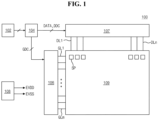
- FIG. 1 is a view showing an organic light emitting diode display device according to a first embodiment of the present disclosure
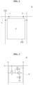
- FIG. 2 is a view showing a subpixel of an organic light emitting diode display device according to a first embodiment of the present disclosure.
- an organic light emitting diode (OLED) display device 100 includes an image processing unit 102, a timing controlling unit 104, a gate driving unit 106, a data driving unit 107, a power supplying unit 108 and a display panel 109.
- the image processing unit 102 outputs an image signal and a plurality of timing signals.
- the plurality of timing signals outputted from the image processing unit 102 may include a data enable signal, a vertical synchronization signal, a horizontal synchronization signal and a clock signal.
- the timing controlling unit 104 receives the image signal and the plurality of timing signals.
- the timing controlling unit 104 generates and outputs a gate control signal GDC for controlling the gate driving unit 106 and a data control signal DDC for controlling the data driving unit 107 based on the plurality of timing signals of the image processing unit 102.
- the timing controlling unit 104 generates and outputs an image data DATA by rearranging the image signal according to the plurality of timing signals.
- the gate driving unit 106 outputs a gate signal (gate voltage) to a plurality of gate lines GL1 to GLm of the display panel 109 in response to the gate control signal GDC supplied from the timing controlling unit 104.
- a gate signal gate voltage
- GDC gate control signal
- the power supplying unit 108 outputs a plurality of voltages including a high level voltage EVDD and a low level voltage EVSS and supplies the plurality of voltages to the display panel 109.
- the high level voltage EVDD is supplied to the display panel 109 through a power line PL (of FIG. 3 ).
- the plurality of voltages outputted from the power suppling unit 108 are supplied to the gate driving unit 106 or the data driving unit 107.
- the display panel 109 displays an image in response to the gate signal and the data signal supplied from the gate driving unit 106 and the data driving unit 107 and the plurality of voltages supplied from the power supplying unit 108.
- one subpixel SP may be connected to a gate line GL, a data line DL and a power line PL.
- a driving method as well as the number of transistors and the number of capacitors may be determined according to a pixel circuit of the subpixel SP.
- FIG. 3 is a view showing a pixel circuit of a subpixel of an organic light emitting diode display device according to a first embodiment of the present disclosure.
- the gate line GL, the data line DL and the power line PL cross each other to define the subpixel SP, and a switching transistor Ts, a driving transistor Td, a storage capacitor Cst and a light emitting diode D are disposed in the subpixel SP.
- the switching transistor Ts is connected to the gate line GL and the data line DL, the driving transistor Td and the storage capacitor Cst are connected between the switching transistor Ts and the power line PL, and the light emitting diode D is connected to the driving transistor Td.
- the driving transistor Td is turned on according to the data signal applied to the gate electrode of the driving transistor Td. As a result, a current proportional to the data signal flows in the light emitting diode D from the power line PL through the driving transistor Td, and the light emitting diode D emits a light of a luminance proportional to the current of the driving transistor Td.
- the storage capacitor Cst is charged with a voltage proportional to the data signal to keep a voltage of the gate electrode of the driving transistor Td constant during a frame.
- the subpixel SP includes two transistors of the switching transistor Ts and the driving transistor Td and one capacitor of the storage capacitor Cst in a first embodiment, the subpixel SP may include three or more transistors and two or more capacitors in another embodiment.
- FIG. 4 is a perspective view showing an organic light emitting diode display device according to a first embodiment of the present disclosure.
- OLED display device 100 may have various structures, an organic light emitting diode on silicon (OLEDoS) structure where a light emitting diode is disposed on a silicon wafer through a semiconductor process will be exemplarily illustrated hereinafter. However, it is not limited thereto.
- OLEDoS organic light emitting diode on silicon
- an organic light emitting diode display device 100 includes a wafer substrate 110, a first electrode 132, an emitting layer 134, a second electrode 136, an encapsulating layer 160 and a color filter layer 180.
- the first electrode 132, the emitting layer 134 and the second electrode 136 constitute a light emitting diode E.
- the wafer substrate 110 may include a silicon wafer through a semiconductor process.
- An active layer may be disposed in the wafer substrate 110, and the gate line, the data line and electrodes of the transistor may be disposed on the wafer substrate 110.
- the first electrode 132, the emitting layer 132 and the second electrode 136 are sequentially disposed on the wafer substrate 110 to constitute a light emitting diode E.
- the first electrodes 132 are spaced apart from each other and disposed in the red subpixel, the green subpixel and the blue subpixel.
- the emitting layer 134 is disposed on the entire wafer substrate 110 to cover the wafer substrate 110 and the first electrode 132.
- the emitting layer 134 is commonly disposed in the red, green and blue subpixels to emit a white colored light.
- the second electrode 136 is disposed on the emitting layer 134.
- the second electrode 136 is disposed in the entire subpixels to supply a signal to the subpixels at the same time.
- the encapsulating layer 160 is disposed on the second electrode 136 to prevent permeation of an oxygen or a moisture into the light emitting diode E.
- the encapsulating layer 160 may have a plurality of layers of inorganic and organic materials.
- the color filter layer 180 is disposed on the encapsulating layer 160.
- the color filter layer 180 may include a red color filter pattern, a green color filter pattern and a blue color filter pattern.
- the active layer is disposed in the wafer substrate 110, a transistor of a single crystalline silicon having an excellent mobility is obtained. As a result, a size of the subpixel is reduced and a display device of a relatively high resolution is obtained.
- transistors in the gate driving unit and the data driving unit as well as the transistor in the subpixel include a single crystalline silicon, a relatively rapid response speed is obtained.
- the OLED display device 100 of an OLEDoS structure may be applied to various fields.
- the OLED display device 100 of an OLEDoS structure may be applied to a device for a metaverse of a virtual world based on a virtual reality and an augmented reality that have been recently highlighted.
- FIG. 5 is a cross-sectional view, which is taken along a line I-I' of FIG. 4 , showing an organic light emitting diode display device according to a first embodiment of the present disclosure.
- the OLED display device 100 includes a transistor T in each of the red, green and blue subpixels SPr (or first subpixel), SPg (or second subpixel) and SPb (or third subpixel) on the wafer substrate 110.
- the transistor T includes an active layer 112 in the wafer substrate 110, a gate insulating layer 122 on the wafer substrate 110, a gate electrode 114 on the gate insulating layer 122, an interlayer insulating layer 124 on the gate electrode 114 over the gate insulating layer 122 and source and drain electrodes 116 and 117 on the interlayer insulating layer 124.
- the wafer substrate 110 may be a single crystalline silicon wafer formed by growing silicon (Si). However, it is not limited thereto.
- the wafer substrate 110 may be a wafer including various semiconductor materials.
- the active layer 112 may be formed inside the wafer substrate 110 and may be partially doped with an impurity. As a result, the active layer 112 may have a channel region 112a not doped with an impurity and at a central portion thereof and source and drain regions 112b and 112c doped with an impurity and at both sides of the channel region 112a.
- the gate insulating layer 122 may have a single layer or a multiple layer including an inorganic material such as silicon oxide (SiOx) and silicon nitride (SiNx). However, it is not limited thereto.
- the interlayer insulating layer 124 may have a single layer or a multiple layer including an inorganic material such as silicon oxide (SiOx) and silicon nitride (SiNx), or an organic material such as photoacryl. Alternatively, the interlayer insulating layer 124 may have a multiple layer of an organic material layer and an inorganic material layer.
- the source and drain electrodes 116 and 117 may have a single layer or a multiple layer including a metallic material such as chromium (Cr), molybdenum (Mo), tantalum (Ta), copper (Cu), titanium (Ti), aluminum (Al) and aluminum alloy. However, it is not limited thereto.
- the source and drain electrodes 116 and 117 are connected to the source and drain regions 112b and 112c, respectively, of the active layer 112 through contact holes in the gate insulating layer 122 and the interlayer insulating layer 124. (ohmic contact)
- a passivation layer 126 may be disposed on the transistor T over the wafer substrate 110.
- the passivation layer 126 may include an organic material such as photoacryl, it is not limited thereto.
- a bank layer 152 is disposed at a boundary portion of each subpixel.
- the bank layer 152 may be a sidewall defining the subpixel.
- the bank layer 152 may divide each subpixel to prevent a mixture of colored lights emitted from adjacent subpixels.
- the light emitting diode E is disposed on the passivation layer 126 and is connected to the drain electrode 117 of the transistor T through a contact hole in the passivation layer 126.
- the light emitting diode E includes a first electrode 132, an emitting layer 134 and a second electrode 136.
- the first electrode 132 is exposed through an opening of the bank layer 152 and is connected to the drain electrode 117 of the transistor T through a contact hole in the passivation layer 126.
- the emitting layer 134 is disposed on the first electrode 132 and the bank layer 152, and the second electrode 136 is disposed on the emitting layer 134.
- the first electrode 132 may include a transparent conductive material such as indium tin oxide (ITO) and indium zinc oxide (IZO) or a metallic material of a relatively thin thickness. However, it is not limited thereto.
- the first electrode 132 is connected to the drain electrode 117 of the transistor T, and a voltage corresponding to the image signal may be applied to the first electrode 132.
- a reflective electrode including a metallic material having a relatively high reflectance such as aluminum (Al) and silver (Ag) may be disposed under the first electrode 132.
- the reflective electrode may reflect a light incident to the first electrode 132 to improve a light efficiency.
- the first electrode 132 is disposed in each subpixel, and a voltage corresponding to the image signal is applied to the first electrode 132 of each subpixel.
- the emitting layer 134 on the first electrode 132 and the bank layer 152 may include at least one of a hole injecting layer, a hole transporting layer, an emitting material layer, an electron transporting layer, and an electron injecting layer.
- the emitting layer 134 may be a white emitting layer which emits a white colored light and is disposed on the entire display device 100.
- the emitting layer 134 may have a tandem structure having at least two stacks. Each stack may include a hole transporting layer, an emitting material layer and an electron transporting layer.
- the emitting material layer may have a tandem structure of a plurality of partial emitting material layers.
- the emitting material layer may include a red partial emitting material layer, a green partial emitting material layer and a blue partial material layer of a tandem structure, and a white colored light may be emitted from the emitting material layer by mixing red, green and blue colored lights emitted from the red, green and blue partial emitting material layers.
- a hole transporting layer, an electron transporting layer and a charge generating layer may be disposed between the plurality of partial emitting material layers.
- the emitting material layer may include a yellow-green partial emitting material layer and a blue partial emitting material layer of a tandem structure, and a white colored light may be emitted from the emitting material layer by mixing yellow-green and blue lights emitted from the yellow-green and blue partial emitting material layers.
- the emitting layer for emitting a white colored light may have various structures other than the above structures.
- the emitting layer 134 may be formed on the entire wafer substrate 110 through a deposition process or a soluble process.
- the second electrode 136 may have a single layer or a multiple layer including a metallic material such as calcium (Ca), barium (Ba), magnesium (Mg), aluminum (Al) and silver (Ag) or an alloy thereof. However, it is not limited thereto.
- the encapsulating layer 160 is disposed on the second electrode 136.
- the encapsulating layer 160 may include a first encapsulating layer 162 of an inorganic material, a second encapsulating layer 164 of an organic material and a third encapsulating layer 166 of an inorganic material.
- the inorganic material may include silicon nitride (SiNx) and silicon oxide (SiOx), it is not limited thereto.
- the organic material may include polyethylene terephthalate, polyethylene naphthalate, polycarbonate, polyimide, polyethylene sulfonate, polyoxymethylene, polyacrylate or a compound thereof. However, it is not limited thereto.
- the encapsulating layer 160 may have various structures other than the above structure of a triple layer.
- the encapsulating layer 160 may have a double layer of an inorganic layer and an organic layer, or a multiple layer of four or more layers.
- the color filter layer 180 is disposed on the encapsulating layer 160.
- the color filter layer 180 includes red, green and blue color filter patterns 180R, 180G and 180B in the red, green and blue subpixels SPr, SPg and SPb, respectively.
- the color filter layer 180 may include a resin such as a color resist. However, it is not limited thereto.
- the color filter layer 180 includes the red, green and blue color filter patterns 180R, 180G and 180B
- the air layer 182 may be regarded as a portion of the color filter layer 180.
- the red color filter pattern 180R absorbs a light of a wavelength band other than a wavelength of the red colored light among the white colored light emitted from the light emitting diode E to output the red colored light.
- the green color filter pattern 180G absorbs a light of a wavelength band other than a wavelength of the green colored light among the white colored light emitted from the light emitting diode E to output the green colored light
- the blue color filter pattern 180B absorbs a light of a wavelength band other than a wavelength of the blue colored light among the white colored light emitted from the light emitting diode E to output the blue colored light.
- An adhesive layer 192 is disposed on the color filter layer 180, and a protecting layer 190 is disposed on the adhesive layer 192 such that the protecting layer 190 is attached to the color filter layer 180 due to the adhesive layer 192.
- the protecting layer 190 protects the OLED display device 100.
- the protecting layer 190 may include a glass or a transparent film.
- the transparent film may include one of a polystyrene (PS) film, a polyethylene (PE) film, a polyethylene naphthalate (PEN) film and a polyimide (PI) film.
- the adhesive layer 192 may include an optical clear adhesive (OCA).
- OCA optical clear adhesive
- the OCA may have a shape of a double-sided tape, and a release film may be disposed on both sides of the OCA. After the release film is detached from the OCA, objects may be attached to both sides of the OCA. As a result, the objects may be attached to each other due to the OCA. Since the OCA is disposed between the color filter layer 180 and the protecting layer 190 in a semisolid state, an adhesive material does not flow into the air layer 182 such that the same shape of the color filter layer 180 is maintained (in other words, such that the color filter layer 180 can always maintain the same shape).
- the adhesive layer 192 is not limited to the OCA, and various adhesive materials may be used for the adhesive layer 192.
- the transistor T is formed on the wafer substrate 110 of a single crystalline semiconductor material instead of a glass or a plastic film, an image of a relatively high quality is obtained even when a size of the subpixel is reduced. As a result, the OLED display device 100 of a high resolution is obtained.
- the OLED display device 100 of an ultra-high resolution is obtained.
- the air layer 182 is disposed between the red, green and blue color filter patterns 180R, 180G and 180B of the color filter layer 180, a light efficiency of the red, green and blue subpixels SPr, SPg and SPb is improved.
- FIG. 6 is a cross-sectional view showing a light path in an organic light emitting diode display device according to a comparison example.
- the color filter layer 180 includes the red, green and blue color filter patterns, and an air layer is not disposed between red, green and blue color filter patterns.
- the white colored light emitted from the light emitting diode E of the red, green and blue subpixels SPr, SPg and SPb is outputted through the color filter layer 180.
- the red color filter pattern absorbs a light of a wavelength band other than a wavelength of the red colored light among the white colored light to output the red colored light.
- the green color filter pattern absorbs a light of a wavelength band other than a wavelength of the green colored light among the white colored light to output the green colored light
- the blue color filter pattern absorbs a light of a wavelength band other than a wavelength of the blue colored light among the white colored light to output the blue colored light.
- the black matrix is not disposed between the red, green and blue color filter patterns, the light emitted from the light emitting diode E of the subpixel may be outputted through the different subpixel.
- first and third lights L1 and L3 perpendicularly emitted from the light emitting diodes E of the red and green subpixels SPr and SPg may be outputted intactly from the red and green subpixels SPr and SPg, respectively.
- the red, green and blue color filter patterns have similar refractive indexes to each other, and the red, green and blue color filter patterns contact each other at an interface between the red, green and blue subpixels.
- a light obliquely emitted from the light emitting diode E enters the adjacent subpixel without refraction through the interface between the red, green and blue color filter patterns and is outputted from the adjacent subpixel.
- a second light L2 obliquely emitted from the light emitting diode E of the red subpixel SPr may enter the green color filter pattern without refraction and reflection through the interface between the red and green color filter patterns and may be outputted from the green subpixel SPg. All of the lights emitted from the light emitting diode E of the red subpixel SPr are not outputted from the red subpixel SPr through the red color filter pattern, and a part of the lights emitted from the light emitting diode E of the red subpixel SPr is outputted from the green subpixel SPg through the green color filter pattern. As a result, the red colored light and the green colored light are mixed in the green subpixel SPg to cause a stain due to a light leakage in the image.
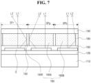
- FIG. 7 is a cross-sectional view showing a light path in an organic light emitting diode display device according to a first embodiment of the present disclosure.
- the color filter layer 180 includes the red, green and blue color filter patterns 180R, 180G and 180B in the red, green and blue subpixels SPr, SPg and SPb, respectively, and the red, green and blue color filter patterns 180R, 180G and 180B are spaced apart from each other such that the air layer 182 is disposed between the red, green and blue color filter patterns 180R, 180G and 180B.
- the white colored light emitted from the light emitting diode E of the red, green and blue subpixels SPr, SPg and SPb is outputted through the color filter layer 180.
- the red color filter pattern 180R may absorb a light of a wavelength band other than a wavelength of the red colored light among the white colored light to output the red colored light.
- the green color filter pattern 180G may absorb a light of a wavelength band other than a wavelength of the green colored light among the white colored light to output the green colored light
- the blue color filter pattern 180B may absorb a light of a wavelength band other than a wavelength of the blue colored light among the white colored light to output the blue colored light.
- First lights L1 perpendicularly emitted from the light emitting diode E of the red, green and blue subpixels SPr, SPg and SPb may be outputted through the red, green and blue color filter patterns 180R, 180G and 180B, respectively.
- Second lights L2 obliquely emitted from the light emitting diode E of the red, green and blue subpixels SPr, SPg and SPb may pass through the red, green and blue color filter patterns 180R, 180G and 180B to reach a side surface of the red, green and blue color filter patterns 180R, 180G and 180B, respectively.
- the air layer 182 is disposed between the red, green and blue color filter patterns 180R, 180G and 180B to contact the side surface of the red, green and blue color filter patterns 180R, 180G and 180B.
- a refractive index of an organic material of the color filter layer 180 is greater than a refractive index of an air of the air layer 182
- the second lights L2 reaching the side surface of the red, green and blue color filter patterns 180R, 180G and 180B do not pass through the air layer 182 and are totally reflected at the side surface of the red, green and blue color filter patterns 180R, 180G and 180B.
- the second lights L2 totally reflected at the side surface of the red, green and blue color filter patterns 180R, 180G and 180B are outputted from the red, green and blue subpixels SPr, SPg and SPb.
- the second light L2 obliquely emitted from the light emitting diode E of the red subpixel SPr may pass through the red color filter pattern 180R to reach the side surface of the red color filter pattern 180R and may be totally reflected at the side surface of the red color filter pattern 180R to be outputted through a top surface of the red color filter pattern 180R.
- the second light L2 obliquely emitted from the light emitting diode E of the green subpixel SPg may pass through the green color filter pattern 180G to reach the side surface of the green color filter pattern 180G and may be totally reflected at the side surface of the green color filter pattern 180G to be outputted through a top surface of the green color filter pattern 180G.
- the second light L2 obliquely emitted from the light emitting diode E of the blue subpixel SPb may pass through the blue color filter pattern 180B to reach the side surface of the blue color filter pattern 180B and may be totally reflected at the side surface of the blue color filter pattern 180B to be outputted through a top surface of the blue color filter pattern 180B.
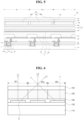
- FIGs. 8A to 8C are graphs showing an emission spectrum of red, green and blue subpixels of an organic light emitting diode display device according to a first embodiment of the present disclosure and an emission spectrum of red, green and blue subpixels of an organic light emitting diode display device according to a comparison example.
- the air layer 182 is disposed between the red, green and blue color filter patterns 180R, 180G and 180B in the OLED display device 100 according to a first embodiment of the present disclosure, and the air layer is not disposed between the red, green and blue color filter patterns in the OLED display device according to a comparison example.
- the red colored light outputted from the red subpixel has an intensity of about 0.11 in a comparison example without the air layer
- the red colored light outputted from the red subpixel SPr has an intensity of about 0.14 in a first embodiment with the air layer 182.
- the red colored light through the red subpixel has an efficiency of about 9.7cd/A in a comparison example without the air layer
- the red colored light through the red subpixel SPr has an efficiency of about 13.6cd/A in a first embodiment with the air layer 182.
- the efficiency of the red colored light of a first embodiment increases by about 40.2% as compared with the efficiency of the red colored light of a comparison example.
- the green colored light outputted from the green subpixel has an intensity of about 0.13 in a comparison example without the air layer
- the green colored light outputted from the green subpixel SPg has an intensity of about 0.136 in a first embodiment with the air layer 182.
- the green colored light through the green subpixel has an efficiency of about 40.4cd/A in a comparison example without the air layer
- the green colored light through the green subpixel SPg has an efficiency of about 42.8cd/A in a first embodiment with the air layer 182.
- the efficiency of the green colored light of a first embodiment increases by about 5.9% as compared with the efficiency of the green colored light of a comparison example.
- the blue colored light outputted from the blue subpixel has an intensity of about 0.20 in a comparison example without the air layer
- the blue colored light outputted from the blue subpixel SPb has an intensity of about 0.30 in a first embodiment with the air layer 182.
- the blue colored light through the blue subpixel SPb has an efficiency of about 5.2cd/A in a first embodiment with the air layer 182.
- the efficiency of the blue colored light of a first embodiment increases by about 85.7% as compared with the efficiency of the blue colored light of a comparison example.
- the light emitted from the light emitting diode E of the subpixel and reaching the side surface of the corresponding color filter pattern is totally reflected at the side surface and is outputted through a top surface of the corresponding color filter pattern.
- the intensity and the efficiency of the red, green and blue colored lights are improved.
- the air layer 182 is disposed between the red, green and blue color filter patterns 180R, 180G and 180B, widths of the red, green and blue color filter patterns 180R, 180G and 180B are reduced. However, deterioration such as a light leakage due to reduction of the widths of the red, green and blue color filter patterns 180R, 180G and 180B is not caused.
- the red colored light outputted from the red subpixel SPr having the red color filter pattern 180R of a width of about 26 ⁇ m has an intensity peak of about 0.16 at a wavelength of about 620nm
- the red colored light outputted from the red subpixel SPr having the red color filter pattern 180R of a width of about 2.1 ⁇ m has an intensity peak of about 0.14 at a wavelength of about 620nm.
- the red colored light through the red color filter pattern 180R of a width about 2.6 ⁇ m and the red colored light through the red color filter pattern 180R of a width about 2.1 ⁇ m have the intensity peak at the same wavelength, and the intensity the red colored light through the red color filter pattern 180R of a width about 2.1 ⁇ m decreases as compared with the intensity the red colored light through the red color filter pattern 180R of a width about 2.6 ⁇ m.
- the red colored light through the red color filter pattern 180R of a width about 2.6 ⁇ m and the red colored light through the red color filter pattern 180R of a width about 2.1 ⁇ m have substantially the same intensity peak width as each other. As a result, a light leakage through the red color filter pattern 180R is not caused even when the width of the red color filter pattern 180R is reduced.
- the intensity of the light is minutely reduced as the width of the color filter pattern is reduced, deterioration such as a light leakage due to reduction of the width is not caused. Further, the reduction of the intensity due to the reduction of the width is minute as compared with increase of the intensity and the efficiency due to the air layer 182. As a result, when the air layer 182 is formed by reducing the width of the color filter pattern, the intensity and the efficiency are improved and deterioration such as a light leakage is prevented.
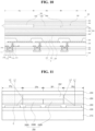
- FIG. 10 is a cross-sectional view showing an organic light emitting diode display device according to a second embodiment of the present disclosure. Illustration on a part the same as a part of a first embodiment may be omitted.
- thicknesses of two of red, green and blue color filter patterns 280R, 280G and 280B is smaller than a thickness of the other one of the red, green and blue color filter patterns 280R, 280G and 280B.
- an air layer is disposed on the two of the red, green and blue color filter patterns 280R, 280G and 280B.
- the thicknesses of the red and blue color filter patterns 280R and 280B are exemplarily smaller than the thickness of the green color filter pattern 280G in a second embodiment.
- the thicknesses of the green and blue color filter patterns 280G and 280B may be exemplarily smaller than the thickness of the red color filter pattern 280R, or the thicknesses of the red and green color filter patterns 280R and 280G may be exemplarily smaller than the thickness of the blue color filter pattern 280B.
- the thickness of one of the red, green and blue color filter patterns 280R, 280G and 280B may be smaller than the thicknesses of the other two of the red, green and blue color filter patterns 280R, 280G and 280B.
- the OLED display device 200 includes a transistor T in each of red, green and blue subpixels SPr, SPg and SPb on a wafer substrate 210.
- the wafer substrate 210 may be a single crystalline silicon wafer.
- the transistor T includes an active layer 212 in the wafer substrate 210, a gate insulating layer 222 on the wafer substrate 210, a gate electrode 214 on the gate insulating layer 222, an interlayer insulating layer 224 on the gate electrode 214 over the gate insulating layer 222 and source and drain electrodes 216 and 217 on the interlayer insulating layer 224.
- the active layer 212 may have a channel region 212a not doped with an impurity and at a central portion thereof and source and drain regions 212b and 212c doped with an impurity and at both sides of the channel region 212a.
- a passivation layer 226 may be disposed on the transistor T over the wafer substrate 210, and a bank layer 252 is disposed at a boundary portion of each subpixel.
- a light emitting diode E is disposed on the passivation layer 226.
- the light emitting diode E includes a first electrode 232, an emitting layer 234 and a second electrode 236.
- the first electrode 232 is exposed through an opening of the bank layer 252 and is connected to a drain electrode 217 of the transistor T through a contact hole in the passivation layer 226.
- the emitting layer 234 is disposed on the first electrode 232 and the bank layer 252, and the second electrode 236 is disposed on the emitting layer 234.
- An encapsulating layer 260 is disposed on the light emitting diode E.
- the encapsulating layer 260 may include a first encapsulating layer 262 of an inorganic material, a second encapsulating layer 264 of an organic material and a third encapsulating layer 266 of an inorganic material.
- a color filter layer 280 is disposed on the encapsulating layer 260.
- the color filter layer 280 includes red, green and blue color filter patterns 280R, 280G and 280B in the red, green and blue subpixels SPr, SPg and SPb, respectively.
- the green color filter pattern 280G has a first thickness t1, and each of the blue and red color filter patterns 280B and 280R has a second thickness t2 smaller than the first thickness t1. (t1>t2)
- the green color filter pattern 280G is formed to have the first thickness t1
- the blue and red color filter patterns 280B and 280R are each formed to have the second thickness t2 smaller than the first thickness t1.
- a vacant space i.e., an air layer 282 is disposed on the blue and red color filter patterns 280B and 280R.
- An adhesive layer 292 such as an optical clear adhesive (OCA) is disposed on the color filter layer 280, and a protecting layer 290 is disposed on the adhesive layer 292 such that the protecting layer 290 is attached to the color filter layer 280 due to the adhesive layer 292.
- OCA optical clear adhesive
- the air layer 282 is disposed on some (e.g., blue and red color filter patterns 280B and 280R) of the red, green and blue color filter patterns 280R, 280G and 280B, a light efficiency of the red, green and blue subpixels SPr, SPg and SPb is improved.
- FIG. 11 is a cross-sectional view showing a light path in an organic light emitting diode display device according to a second embodiment of the present disclosure.
- the color filter layer 280 includes the red, green and blue color filter patterns 280R, 280G and 280B in the red, green and blue subpixels SPr, SPg and SPb, respectively, and the air layer 282 is disposed on the blue and red color filter patterns 280B and 280R.
- the air layer 282 is disposed between the upper portions of the green color filter patterns 280G.
- First lights L1 perpendicularly emitted from the light emitting diode E of the red, green and blue subpixels SPr, SPg and SPb may be outputted through the red, green and blue color filter patterns 280R, 280G and 280B, respectively.
- a second light L2 obliquely emitted from the light emitting diode E of the green subpixel SPg may pass through the green color filter pattern 280G to reach a side surface of the upper portion of the green color filter pattern 280G.
- the air layer 282 is disposed on the blue and red color filter patterns 280B and 280R to contact the side surface of the upper portion of the green color filter pattern 280G.
- a refractive index of an organic material of the color filter layer 280 is greater than a refractive index of an air of the air layer 282
- the second light L2 reaching the side surface of the upper portion of the green color filter pattern 280G do not pass through the air layer 282 and are totally reflected at the side surface of the upper portion of the green color filter pattern 280G.
- the second light L2 totally reflected at the side surface of the upper portion of the green color filter pattern 280G is outputted from the green subpixel SPg.
- FIG. 12 is a cross-sectional view showing an organic light emitting diode display device according to a third embodiment of the present disclosure.
- a light emitting diode E is disposed in each of red, green and blue subpixels SPr, SPg and SPb on a wafer substrate 310, and an encapsulating layer 360 is disposed on the light emitting diode E.
- a color filter layer 380 is disposed on the encapsulation layer 360, and a protecting layer 390 is disposed on the color filter layer 380 with an adhesive layer interposed therebetween.
- the color filter layer 380 includes red, green and blue color filter patterns 380R, 380G and 380B in the red, green and blue subpixels SPr, SPg and SPb, respectively.
- One or two of the red, green and blue color filter patterns 380R, 380G and 380B may have a first thickness
- the other one or two of the red, green and blue color filter patterns 380R, 380G and 380B may have a second thickness smaller than the first thickness.
- a first air layer 382a is disposed on the other one or two of the red, green and blue color filter patterns 380R, 380G and 380B having the second thickness.
- a vacant space where the red, green and blue color filter patterns 380R, 380G and 380B are not formed i.e., a second air layer 382b filled with an air, is disposed in a boundary portion of the red, green and blue subpixels SPr, SPg and SPb between the red, green and blue color filter patterns 380R, 380G and 380B.
- the first air layer 382a on the color filter pattern having the second thickness and the second air layer 382b between the color filter patterns may communicate with each other.
- the OLED display device since the light obliquely emitted from the light emitting diode E of the subpixel is totally reflected at an interface between the corresponding color filter pattern and the air layer such as the first and second air layers 382a and 382b to be outputted through the corresponding color filter pattern, deterioration due to a color mixture of the adjacent subpixels is prevented and a luminance of the corresponding subpixel increases.
- the black matrix is not disposed between the color filter patterns, a subminiature display device of a relatively high resolution is obtained.
- the air layer is disposed between the color filter patterns, and the light is totally reflected at the interface between the color filter pattern and the air layer to be outputted through the corresponding color filter pattern.
- the luminance of the corresponding subpixel increases and the light efficiency is improved.
Landscapes
- Physics & Mathematics (AREA)
- Engineering & Computer Science (AREA)
- Microelectronics & Electronic Packaging (AREA)
- Optics & Photonics (AREA)
- Geometry (AREA)
- General Physics & Mathematics (AREA)
- Theoretical Computer Science (AREA)
- Electroluminescent Light Sources (AREA)
- Devices For Indicating Variable Information By Combining Individual Elements (AREA)
Abstract
Description
- The present application claims the priority benefit of Republic of
Korea Patent Application No. 10-2021-0194517 filed in Republic of Korea on December 31, 2021 - The present disclosure relates to a display device, and more particularly, to a display device where a light efficiency is improved.
- Recently, a flat panel display (FPD) device has been the subject of research and development with the advent of a multimedia. As a result, a flat panel display device such as a liquid crystal display (LCD) device, a plasma display panel (PDP) device and an organic light emitting diode (OLED) display device has been commercialized. Among various FPD devices, the OLED display device has been widely used due to a high response speed, a high luminance and a wide viewing angle.
- As a virtual reality and an augmented reality has been highlighted, a demand for a display device having a high resolution and a compact structure has increased. However, it is difficult that the conventional OLED display device satisfies the high resolution and the compact structure.
- Accordingly, the present disclosure is directed to a display device that substantially obviates one or more of the problems due to limitations and disadvantages of the related art.
- An object of the present disclosure is to provide a display device where deterioration due to a color mixture with an adjacent subpixel is prevented and a light efficiency is improved.
- Additional features and advantages of the present disclosure will be set forth in the description which follows, and in part will be apparent from the description, or may be learned by practice of the disclosure. These and other advantages of the present disclosure will be realized and attained by the structure particularly pointed out in the written description and claims hereof as well as the appended drawings.
- To achieve these and other advantages and in accordance with the purpose of the present disclosure, as embodied and broadly described herein, a display device includes: a substrate including first, second and third subpixels; a light emitting diode in each of the first, second and third subpixels on the substrate; a color filter layer on the light emitting diode, the color filter layer including first, second and third color filter patterns in the first, second and third subpixels, respectively; and an air layer in the color filter layer.
- In one or more embodiments, the substrate includes a semiconductor wafer.
- In one or more embodiments, the display device further comprises a transistor in each of the first, second and third subpixels on the substrate, wherein the transistor comprises: an active layer in the substrate; a gate insulating layer on the active layer; a gate electrode on the gate insulating layer; an interlayer insulating layer on the gate electrode; a source electrode and a drain electrode on the interlayer insulating layer; and a passivation layer on the source electrode and the drain electrode.
- In one or more embodiments, the air layer is disposed in a boundary portion of the first, second and third subpixels between the first, second and third color filter patterns.
- In one or more embodiments, at least one of the first, second and third color filter patterns has a first thickness and other one or two of the first, second and third color filter patterns has a second thickness smaller than the first thickness, wherein the air layer is disposed on the other one or two of the first, second and third color filter patterns having the second thickness.
- In one or more embodiments, at least one of the first, second and third color filter patterns has a first thickness and other one or two of the first, second and third color filter patterns has a second thickness smaller than the first thickness, and the air layer includes a first air layer disposed on the other one or two of the first, second and third color filter patterns having the second thickness and a second air layer disposed in a boundary portion of the first, second and third subpixels between the first, second and third color filter patterns.
- In one or more embodiments, the first and second air layers communicate with each other.
- In one or more embodiments, the display device further comprises an encapsulating layer on the light emitting diode.
- In one or more embodiments, the encapsulating layer comprises: a first encapsulating layer on the light emitting diode; a second encapsulating layer on the first encapsulating layer; and a third encapsulating layer on the second encapsulating layer.
- In one or more embodiments, the light emitting diode comprises: a first electrode on the interlayer insulating layer; an emitting layer on the first electrode; and a second electrode on the emitting layer.
- In one or more embodiments, the emitting layer is configured to emit a white colored light.
- In one or more embodiments, the first, second and third subpixels correspond to red, green and blue subpixels, respectively.
- In one or more embodiments, the transistor (e.g., the active layer of the transistor) includes single crystalline silicon.
- In one or more embodiments, the display device further comprises an adhesive layer on the color filter layer and a protecting layer on the adhesive layer, wherein the protecting layer is attached to the color filter layer due to the adhesive layer.
- In one or more embodiments, the adhesive layer includes an optical clear adhesive in a semisolid state.
- In one or more embodiments, light obliquely emitted from the light emitting diode of the first subpixel passes through the first color filter pattern to reach a side surface of the first color filter pattern and is totally reflected at the side surface of the first color filter pattern to be outputted through a top surface of the first color filter pattern, light obliquely emitted from the light emitting diode of the second subpixel passes through the second color filter pattern to reach a side surface of the second color filter pattern and is totally reflected at the side surface of the second color filter pattern to be outputted through a top surface of the second color filter pattern, and light obliquely emitted from the light emitting diode of the third subpixel passes through the third color filter pattern to reach a side surface of the third color filter pattern and is totally reflected at the side surface of the third color filter pattern to be outputted through a top surface of the third color filter pattern.
- In one or more embodiments, light obliquely emitted from the light emitting diode of a corresponding subpixel of the first, second and third subpixels is totally reflected at an interface between a corresponding color filter pattern of the first, second and third color filter patterns and the air layer to be outputted through the corresponding color filter pattern.
- It is to be understood that both the foregoing general description and the following detailed description are explanatory and are intended to provide further explanation of the disclosure as claimed.
- The accompanying drawings, which are included to provide a further understanding of the present disclosure and are incorporated in and constitute a part of this specification, illustrate embodiments of the present disclosure and together with the description serve to explain the principles of the present disclosure. In the drawings:
-
FIG. 1 is a view showing an organic light emitting diode display device according to a first embodiment of the present disclosure; -
FIG. 2 is a view showing a subpixel of an organic light emitting diode display device according to a first embodiment of the present disclosure; -
FIG. 3 is a view showing a pixel circuit of a subpixel of an organic light emitting diode display device according to a first embodiment of the present disclosure; -
FIG. 4 is a perspective view showing an organic light emitting diode display device according to a first embodiment of the present disclosure; -
FIG. 5 is a cross-sectional view, which is taken along a line I-I' ofFIG. 4 , showing an organic light emitting diode display device according to a first embodiment of the present disclosure; -
FIG. 6 is a cross-sectional view showing a light path in an organic light emitting diode display device according to a comparison example; -
FIG. 7 is a cross-sectional view showing a light path in an organic light emitting diode display device according to a first embodiment of the present disclosure ; -
FIG. 8A is graph showing an emission spectrum of a red subpixel of an organic light emitting diode display device according to a first embodiment of the present disclosure and an emission spectrum of a red subpixel of an organic light emitting diode display device according to a comparison example; -
FIG. 8B is a graph showing an emission spectrum of a green subpixel of an organic light emitting diode display device according to a first embodiment of the present disclosure and an emission spectrum of a green subpixel of an organic light emitting diode display device according to a comparison example; -
FIG. 8C is a graph showing an emission spectrum of a blue subpixel of an organic light emitting diode display device according to a first embodiment of the present disclosure and an emission spectrum of a blue subpixel of an organic light emitting diode display device according to a comparison example; -
FIG. 9 is a graph showing an emission spectrum with respect to a width of a color filter pattern of an organic light emitting diode display device according to a first embodiment of the present disclosure; -
FIG. 10 is a cross-sectional view showing an organic light emitting diode display device according to a second embodiment of the present disclosure; -
FIG. 11 is a cross-sectional view showing a light path in an organic light emitting diode display device according to a second embodiment of the present disclosure; and -
FIG. 12 is a cross-sectional view showing an organic light emitting diode display device according to a third embodiment of the present disclosure. - Advantages and features of the present disclosure, and implementation methods thereof will be clarified through following example embodiments described with reference to the accompanying drawings. The present disclosure may, however, be embodied in different forms and should not be construed as limited to the example embodiments set forth herein. Rather, these example embodiments are provided so that this disclosure may be sufficiently thorough and complete to assist those skilled in the art to fully understand the scope of the present disclosure. Further, the present disclosure is only defined by scopes of claims.
- A shape, a size, a ratio, an angle, and a number disclosed in the drawings for describing embodiments of the present disclosure are merely an example. Thus, the present disclosure is not limited to the illustrated details. Like reference numerals refer to like elements throughout. In the following description, when the detailed description of the relevant known function or configuration is determined to unnecessarily obscure an important point of the present disclosure, the detailed description of such known function or configuration may be omitted. In a case where terms "comprise," "have," and "include" described in the present specification are used, another part may be added unless a more limiting term, such as "only," is used. The terms of a singular form may include plural forms unless referred to the contrary.
- In construing an element, the element is construed as including an error or tolerance range even where no explicit description of such an error or tolerance range.
- In describing a position relationship, when a position relation between two parts is described as, for example, "on," "over," "under," or "next," one or more other parts may be disposed between the two parts unless a more limiting term, such as "just" or "direct(ly)," is used.
- It will be understood that, although the terms "first," "second," etc. may be used herein to describe various elements, these elements should not be limited by these terms. These terms are only used to distinguish one element from another. For example, a first element could be termed a second element, and, similarly, a second element could be termed a first element, without departing from the scope of the present disclosure.
- Features of various embodiments of the present disclosure may be partially or overall coupled to or combined with each other, and may be variously inter-operated with each other and driven technically as those skilled in the art can sufficiently understand. Embodiments of the present disclosure may be carried out independently from each other, or may be carried out together in co-dependent relationship.
- Hereinafter, a display device according to embodiments of the present disclosure will be described in detail with reference to the accompanying drawings. In the following description, like reference numerals designate like elements throughout. When a detailed description of well-known functions or configurations related to this document is determined to unnecessarily cloud a gist of the inventive concept, the detailed description thereof will be omitted or will be made brief.
- The present disclosure may be applied to various display devices. For example, although the present disclosure may be applied to various display devices such as an organic light emitting diode display device and an electrophoretic display device, the organic light emitting diode display device will be exemplarily illustrated hereinafter.
-
FIG. 1 is a view showing an organic light emitting diode display device according to a first embodiment of the present disclosure, andFIG. 2 is a view showing a subpixel of an organic light emitting diode display device according to a first embodiment of the present disclosure. - In
FIG. 1 , an organic light emitting diode (OLED)display device 100 according to a first embodiment of the present disclosure includes animage processing unit 102, atiming controlling unit 104, agate driving unit 106, adata driving unit 107, apower supplying unit 108 and adisplay panel 109. - The
image processing unit 102 outputs an image signal and a plurality of timing signals. For example, the plurality of timing signals outputted from theimage processing unit 102 may include a data enable signal, a vertical synchronization signal, a horizontal synchronization signal and a clock signal. - The
timing controlling unit 104 receives the image signal and the plurality of timing signals. Thetiming controlling unit 104 generates and outputs a gate control signal GDC for controlling thegate driving unit 106 and a data control signal DDC for controlling thedata driving unit 107 based on the plurality of timing signals of theimage processing unit 102. Thetiming controlling unit 104 generates and outputs an image data DATA by rearranging the image signal according to the plurality of timing signals. - The
gate driving unit 106 outputs a gate signal (gate voltage) to a plurality of gate lines GL1 to GLm of thedisplay panel 109 in response to the gate control signal GDC supplied from thetiming controlling unit 104. Although thegate driving unit 106 may have an integrated circuit (IC) shape, it is not limited thereto. - The
data driving unit 107 outputs a data signal (data voltage) to a plurality of data lines DL1 to DLn of thedisplay panel 109 in response to the data control signal DDC and the image data DATA. Thedata driving unit 107 may convert the image data DATA of a digital type supplied from thetiming controlling unit 104 into the data signal of an analog type based on a gamma voltage through a sampling and a latch. Although thedata driving unit 107 may have an integrated circuit (IC) shape, it is not limited thereto. - The
power supplying unit 108 outputs a plurality of voltages including a high level voltage EVDD and a low level voltage EVSS and supplies the plurality of voltages to thedisplay panel 109. The high level voltage EVDD is supplied to thedisplay panel 109 through a power line PL (ofFIG. 3 ). The plurality of voltages outputted from thepower suppling unit 108 are supplied to thegate driving unit 106 or thedata driving unit 107. - The
display panel 109 displays an image in response to the gate signal and the data signal supplied from thegate driving unit 106 and thedata driving unit 107 and the plurality of voltages supplied from thepower supplying unit 108. - The
display panel 109 includes a plurality of subpixels SP to display an image. The plurality of subpixels SP may include a red subpixel, a green subpixel and a blue subpixel or a white subpixel, a red subpixel, a green subpixel and a blue subpixel. Although the white, red, green and blue subpixels may have the same area as each other, it is not limited thereto. - In
FIG. 2 , one subpixel SP may be connected to a gate line GL, a data line DL and a power line PL. A driving method as well as the number of transistors and the number of capacitors may be determined according to a pixel circuit of the subpixel SP. -
FIG. 3 is a view showing a pixel circuit of a subpixel of an organic light emitting diode display device according to a first embodiment of the present disclosure. - In
FIG. 3 , the gate line GL, the data line DL and the power line PL cross each other to define the subpixel SP, and a switching transistor Ts, a driving transistor Td, a storage capacitor Cst and a light emitting diode D are disposed in the subpixel SP. - The switching transistor Ts is connected to the gate line GL and the data line DL, the driving transistor Td and the storage capacitor Cst are connected between the switching transistor Ts and the power line PL, and the light emitting diode D is connected to the driving transistor Td.
- In the OLED display device, when the switching transistor Ts is turned on according to the gate signal of the gate line GL, the data signal of the data line DL is applied to a gate electrode of the driving transistor Td and an electrode of the storage capacitor Cst through the switching transistor Ts.
- The driving transistor Td is turned on according to the data signal applied to the gate electrode of the driving transistor Td. As a result, a current proportional to the data signal flows in the light emitting diode D from the power line PL through the driving transistor Td, and the light emitting diode D emits a light of a luminance proportional to the current of the driving transistor Td.
- The storage capacitor Cst is charged with a voltage proportional to the data signal to keep a voltage of the gate electrode of the driving transistor Td constant during a frame.
- Although the subpixel SP includes two transistors of the switching transistor Ts and the driving transistor Td and one capacitor of the storage capacitor Cst in a first embodiment, the subpixel SP may include three or more transistors and two or more capacitors in another embodiment.
-
FIG. 4 is a perspective view showing an organic light emitting diode display device according to a first embodiment of the present disclosure. - Although the
OLED display device 100 according to a first embodiment of the present disclosure may have various structures, an organic light emitting diode on silicon (OLEDoS) structure where a light emitting diode is disposed on a silicon wafer through a semiconductor process will be exemplarily illustrated hereinafter. However, it is not limited thereto. - In
FIG. 4 , an organic light emittingdiode display device 100 according to a first embodiment of the present disclosure includes awafer substrate 110, afirst electrode 132, an emittinglayer 134, asecond electrode 136, anencapsulating layer 160 and acolor filter layer 180. - The
first electrode 132, the emittinglayer 134 and thesecond electrode 136 constitute a light emitting diode E. - The
wafer substrate 110 may include a silicon wafer through a semiconductor process. An active layer may be disposed in thewafer substrate 110, and the gate line, the data line and electrodes of the transistor may be disposed on thewafer substrate 110. - The
first electrode 132, the emittinglayer 132 and thesecond electrode 136 are sequentially disposed on thewafer substrate 110 to constitute a light emitting diode E. Thefirst electrodes 132 are spaced apart from each other and disposed in the red subpixel, the green subpixel and the blue subpixel. - The emitting
layer 134 is disposed on theentire wafer substrate 110 to cover thewafer substrate 110 and thefirst electrode 132. The emittinglayer 134 is commonly disposed in the red, green and blue subpixels to emit a white colored light. - The
second electrode 136 is disposed on the emittinglayer 134. Thesecond electrode 136 is disposed in the entire subpixels to supply a signal to the subpixels at the same time. - The
encapsulating layer 160 is disposed on thesecond electrode 136 to prevent permeation of an oxygen or a moisture into the light emitting diode E.The encapsulating layer 160 may have a plurality of layers of inorganic and organic materials. - The
color filter layer 180 is disposed on theencapsulating layer 160. Thecolor filter layer 180 may include a red color filter pattern, a green color filter pattern and a blue color filter pattern. - In the
OLED display device 100 of the OLEDoS structure according to a first embodiment of the present disclosure, since the active layer is disposed in thewafer substrate 110, a transistor of a single crystalline silicon having an excellent mobility is obtained. As a result, a size of the subpixel is reduced and a display device of a relatively high resolution is obtained. - Further, since transistors in the gate driving unit and the data driving unit as well as the transistor in the subpixel include a single crystalline silicon, a relatively rapid response speed is obtained.
- The
OLED display device 100 of an OLEDoS structure may be applied to various fields. For example, theOLED display device 100 of an OLEDoS structure may be applied to a device for a metaverse of a virtual world based on a virtual reality and an augmented reality that have been recently highlighted. -
FIG. 5 is a cross-sectional view, which is taken along a line I-I' ofFIG. 4 , showing an organic light emitting diode display device according to a first embodiment of the present disclosure. - In
FIG. 5 , theOLED display device 100 according to a first embodiment of the present disclosure includes a transistor T in each of the red, green and blue subpixels SPr (or first subpixel), SPg (or second subpixel) and SPb (or third subpixel) on thewafer substrate 110. - The transistor T includes an
active layer 112 in thewafer substrate 110, agate insulating layer 122 on thewafer substrate 110, agate electrode 114 on thegate insulating layer 122, aninterlayer insulating layer 124 on thegate electrode 114 over thegate insulating layer 122 and source and drainelectrodes interlayer insulating layer 124. - The
wafer substrate 110 may be a single crystalline silicon wafer formed by growing silicon (Si). However, it is not limited thereto. For example, thewafer substrate 110 may be a wafer including various semiconductor materials. - The
active layer 112 may be formed inside thewafer substrate 110 and may be partially doped with an impurity. As a result, theactive layer 112 may have achannel region 112a not doped with an impurity and at a central portion thereof and source and drainregions channel region 112a. - The
gate insulating layer 122 may have a single layer or a multiple layer including an inorganic material such as silicon oxide (SiOx) and silicon nitride (SiNx). However, it is not limited thereto. - The interlayer insulating
layer 124 may have a single layer or a multiple layer including an inorganic material such as silicon oxide (SiOx) and silicon nitride (SiNx), or an organic material such as photoacryl. Alternatively, theinterlayer insulating layer 124 may have a multiple layer of an organic material layer and an inorganic material layer. - The source and drain
electrodes - The source and drain
electrodes regions active layer 112 through contact holes in thegate insulating layer 122 and the interlayer insulatinglayer 124. (ohmic contact) - A
passivation layer 126 may be disposed on the transistor T over thewafer substrate 110. Although thepassivation layer 126 may include an organic material such as photoacryl, it is not limited thereto. - A
bank layer 152 is disposed at a boundary portion of each subpixel. Thebank layer 152 may be a sidewall defining the subpixel. Thebank layer 152 may divide each subpixel to prevent a mixture of colored lights emitted from adjacent subpixels. - The light emitting diode E is disposed on the
passivation layer 126 and is connected to thedrain electrode 117 of the transistor T through a contact hole in thepassivation layer 126. - The light emitting diode E includes a
first electrode 132, an emittinglayer 134 and asecond electrode 136. Thefirst electrode 132 is exposed through an opening of thebank layer 152 and is connected to thedrain electrode 117 of the transistor T through a contact hole in thepassivation layer 126. The emittinglayer 134 is disposed on thefirst electrode 132 and thebank layer 152, and thesecond electrode 136 is disposed on the emittinglayer 134. - The
first electrode 132 may include a transparent conductive material such as indium tin oxide (ITO) and indium zinc oxide (IZO) or a metallic material of a relatively thin thickness. However, it is not limited thereto. Thefirst electrode 132 is connected to thedrain electrode 117 of the transistor T, and a voltage corresponding to the image signal may be applied to thefirst electrode 132. - When the
first electrode 132 includes a transparent metal oxide, a reflective electrode including a metallic material having a relatively high reflectance such as aluminum (Al) and silver (Ag) may be disposed under thefirst electrode 132. The reflective electrode may reflect a light incident to thefirst electrode 132 to improve a light efficiency. - The
first electrode 132 is disposed in each subpixel, and a voltage corresponding to the image signal is applied to thefirst electrode 132 of each subpixel. - The emitting
layer 134 on thefirst electrode 132 and thebank layer 152 may include at least one of a hole injecting layer, a hole transporting layer, an emitting material layer, an electron transporting layer, and an electron injecting layer. - The emitting
layer 134 may be a white emitting layer which emits a white colored light and is disposed on theentire display device 100. The emittinglayer 134 may have a tandem structure having at least two stacks. Each stack may include a hole transporting layer, an emitting material layer and an electron transporting layer. - The emitting material layer may have a tandem structure of a plurality of partial emitting material layers. For example, the emitting material layer may include a red partial emitting material layer, a green partial emitting material layer and a blue partial material layer of a tandem structure, and a white colored light may be emitted from the emitting material layer by mixing red, green and blue colored lights emitted from the red, green and blue partial emitting material layers. A hole transporting layer, an electron transporting layer and a charge generating layer may be disposed between the plurality of partial emitting material layers.
- Further, the emitting material layer may include a yellow-green partial emitting material layer and a blue partial emitting material layer of a tandem structure, and a white colored light may be emitted from the emitting material layer by mixing yellow-green and blue lights emitted from the yellow-green and blue partial emitting material layers.
- In the
OLED display device 100 according to a first embodiment of the present disclosure, the emitting layer for emitting a white colored light may have various structures other than the above structures. The emittinglayer 134 may be formed on theentire wafer substrate 110 through a deposition process or a soluble process. - The
second electrode 136 may have a single layer or a multiple layer including a metallic material such as calcium (Ca), barium (Ba), magnesium (Mg), aluminum (Al) and silver (Ag) or an alloy thereof. However, it is not limited thereto. - When a voltage is applied to the first and
second electrodes layer 134 through the hole transporting layer and the electron transporting layer and are combined with each other to emit a light. - The
encapsulating layer 160 is disposed on thesecond electrode 136. Theencapsulating layer 160 may include afirst encapsulating layer 162 of an inorganic material, asecond encapsulating layer 164 of an organic material and athird encapsulating layer 166 of an inorganic material. Although the inorganic material may include silicon nitride (SiNx) and silicon oxide (SiOx), it is not limited thereto. The organic material may include polyethylene terephthalate, polyethylene naphthalate, polycarbonate, polyimide, polyethylene sulfonate, polyoxymethylene, polyacrylate or a compound thereof. However, it is not limited thereto. - In the
OLED display device 100 according to a first embodiment of the present disclosure, theencapsulating layer 160 may have various structures other than the above structure of a triple layer. For example, theencapsulating layer 160 may have a double layer of an inorganic layer and an organic layer, or a multiple layer of four or more layers. - The
color filter layer 180 is disposed on theencapsulating layer 160. Thecolor filter layer 180 includes red, green and bluecolor filter patterns color filter layer 180 may include a resin such as a color resist. However, it is not limited thereto. - A vacant space where the red, green and blue
color filter patterns air layer 182 filled with an air, is disposed in a boundary portion of the red, green and blue subpixels SPr, SPg and SPb between the red, green and bluecolor filter patterns color filter layer 180 includes the red, green and bluecolor filter patterns air layer 182 may be regarded as a portion of thecolor filter layer 180. - The red
color filter pattern 180R absorbs a light of a wavelength band other than a wavelength of the red colored light among the white colored light emitted from the light emitting diode E to output the red colored light. The greencolor filter pattern 180G absorbs a light of a wavelength band other than a wavelength of the green colored light among the white colored light emitted from the light emitting diode E to output the green colored light, and the bluecolor filter pattern 180B absorbs a light of a wavelength band other than a wavelength of the blue colored light among the white colored light emitted from the light emitting diode E to output the blue colored light. - An
adhesive layer 192 is disposed on thecolor filter layer 180, and aprotecting layer 190 is disposed on theadhesive layer 192 such that the protectinglayer 190 is attached to thecolor filter layer 180 due to theadhesive layer 192. - The protecting
layer 190 protects theOLED display device 100. For example, the protectinglayer 190 may include a glass or a transparent film. The transparent film may include one of a polystyrene (PS) film, a polyethylene (PE) film, a polyethylene naphthalate (PEN) film and a polyimide (PI) film. - The
adhesive layer 192 may include an optical clear adhesive (OCA). The OCA may have a shape of a double-sided tape, and a release film may be disposed on both sides of the OCA. After the release film is detached from the OCA, objects may be attached to both sides of the OCA. As a result, the objects may be attached to each other due to the OCA. Since the OCA is disposed between thecolor filter layer 180 and theprotecting layer 190 in a semisolid state, an adhesive material does not flow into theair layer 182 such that the same shape of thecolor filter layer 180 is maintained (in other words, such that thecolor filter layer 180 can always maintain the same shape). - The
adhesive layer 192 is not limited to the OCA, and various adhesive materials may be used for theadhesive layer 192. - In the
OLED display device 100 according to a first embodiment of the present disclosure, since the transistor T is formed on thewafer substrate 110 of a single crystalline semiconductor material instead of a glass or a plastic film, an image of a relatively high quality is obtained even when a size of the subpixel is reduced. As a result, theOLED display device 100 of a high resolution is obtained. - Further, since a black matrix for preventing a light leakage is not disposed between the subpixels SPr, SPg and SPb, a size of the subpixel is reduced. As a result, the
OLED display device 100 of an ultra-high resolution is obtained. - In addition, since the
air layer 182 is disposed between the red, green and bluecolor filter patterns color filter layer 180, a light efficiency of the red, green and blue subpixels SPr, SPg and SPb is improved. -
FIG. 6 is a cross-sectional view showing a light path in an organic light emitting diode display device according to a comparison example. - In
FIG. 6 , thecolor filter layer 180 includes the red, green and blue color filter patterns, and an air layer is not disposed between red, green and blue color filter patterns. The white colored light emitted from the light emitting diode E of the red, green and blue subpixels SPr, SPg and SPb is outputted through thecolor filter layer 180. The red color filter pattern absorbs a light of a wavelength band other than a wavelength of the red colored light among the white colored light to output the red colored light. The green color filter pattern absorbs a light of a wavelength band other than a wavelength of the green colored light among the white colored light to output the green colored light, and the blue color filter pattern absorbs a light of a wavelength band other than a wavelength of the blue colored light among the white colored light to output the blue colored light. - Since the black matrix is not disposed between the red, green and blue color filter patterns, the light emitted from the light emitting diode E of the subpixel may be outputted through the different subpixel.
- For example, first and third lights L1 and L3 perpendicularly emitted from the light emitting diodes E of the red and green subpixels SPr and SPg may be outputted intactly from the red and green subpixels SPr and SPg, respectively.
- The red, green and blue color filter patterns have similar refractive indexes to each other, and the red, green and blue color filter patterns contact each other at an interface between the red, green and blue subpixels. As a result, a light obliquely emitted from the light emitting diode E enters the adjacent subpixel without refraction through the interface between the red, green and blue color filter patterns and is outputted from the adjacent subpixel.
- For example, a second light L2 obliquely emitted from the light emitting diode E of the red subpixel SPr may enter the green color filter pattern without refraction and reflection through the interface between the red and green color filter patterns and may be outputted from the green subpixel SPg. All of the lights emitted from the light emitting diode E of the red subpixel SPr are not outputted from the red subpixel SPr through the red color filter pattern, and a part of the lights emitted from the light emitting diode E of the red subpixel SPr is outputted from the green subpixel SPg through the green color filter pattern. As a result, the red colored light and the green colored light are mixed in the green subpixel SPg to cause a stain due to a light leakage in the image.
- Further, since a part of the light emitted from the subpixel is outputted from the adjacent subpixel, an intensity of the light outputted from the subpixel is reduced and a light efficiency of the
OLED display device 100 is reduced. -
FIG. 7 is a cross-sectional view showing a light path in an organic light emitting diode display device according to a first embodiment of the present disclosure. - In
FIG. 7 , thecolor filter layer 180 includes the red, green and bluecolor filter patterns color filter patterns air layer 182 is disposed between the red, green and bluecolor filter patterns - In the
OLED display device 100 according to a first embodiment of the present disclosure, the white colored light emitted from the light emitting diode E of the red, green and blue subpixels SPr, SPg and SPb is outputted through thecolor filter layer 180. For example, the redcolor filter pattern 180R may absorb a light of a wavelength band other than a wavelength of the red colored light among the white colored light to output the red colored light. The greencolor filter pattern 180G may absorb a light of a wavelength band other than a wavelength of the green colored light among the white colored light to output the green colored light, and the bluecolor filter pattern 180B may absorb a light of a wavelength band other than a wavelength of the blue colored light among the white colored light to output the blue colored light. - First lights L1 perpendicularly emitted from the light emitting diode E of the red, green and blue subpixels SPr, SPg and SPb may be outputted through the red, green and blue
color filter patterns - Second lights L2 obliquely emitted from the light emitting diode E of the red, green and blue subpixels SPr, SPg and SPb may pass through the red, green and blue
color filter patterns color filter patterns air layer 182 is disposed between the red, green and bluecolor filter patterns color filter patterns - Since a refractive index of an organic material of the
color filter layer 180 is greater than a refractive index of an air of theair layer 182, the second lights L2 reaching the side surface of the red, green and bluecolor filter patterns air layer 182 and are totally reflected at the side surface of the red, green and bluecolor filter patterns color filter patterns - For example, the second light L2 obliquely emitted from the light emitting diode E of the red subpixel SPr may pass through the red
color filter pattern 180R to reach the side surface of the redcolor filter pattern 180R and may be totally reflected at the side surface of the redcolor filter pattern 180R to be outputted through a top surface of the redcolor filter pattern 180R. Similarly, the second light L2 obliquely emitted from the light emitting diode E of the green subpixel SPg may pass through the greencolor filter pattern 180G to reach the side surface of the greencolor filter pattern 180G and may be totally reflected at the side surface of the greencolor filter pattern 180G to be outputted through a top surface of the greencolor filter pattern 180G. Further, the second light L2 obliquely emitted from the light emitting diode E of the blue subpixel SPb may pass through the bluecolor filter pattern 180B to reach the side surface of the bluecolor filter pattern 180B and may be totally reflected at the side surface of the bluecolor filter pattern 180B to be outputted through a top surface of the bluecolor filter pattern 180B. - Accordingly, in the
OLED display device 100 according to a first embodiment of the present disclosure, since the light emitted from the light emitting diode E of the subpixel does not permeate into the adjacent subpixel and is outputted through the corresponding color filter pattern, deterioration due to a color mixture of the adjacent subpixels is prevented and a luminance of the corresponding subpixel increases. -
FIGs. 8A to 8C are graphs showing an emission spectrum of red, green and blue subpixels of an organic light emitting diode display device according to a first embodiment of the present disclosure and an emission spectrum of red, green and blue subpixels of an organic light emitting diode display device according to a comparison example. Theair layer 182 is disposed between the red, green and bluecolor filter patterns OLED display device 100 according to a first embodiment of the present disclosure, and the air layer is not disposed between the red, green and blue color filter patterns in the OLED display device according to a comparison example. - In
FIG. 8A , while the red colored light outputted from the red subpixel has an intensity of about 0.11 in a comparison example without the air layer, the red colored light outputted from the red subpixel SPr has an intensity of about 0.14 in a first embodiment with theair layer 182. As a result, while the red colored light through the red subpixel has an efficiency of about 9.7cd/A in a comparison example without the air layer, the red colored light through the red subpixel SPr has an efficiency of about 13.6cd/A in a first embodiment with theair layer 182. The efficiency of the red colored light of a first embodiment increases by about 40.2% as compared with the efficiency of the red colored light of a comparison example. - In
FIG. 8B , while the green colored light outputted from the green subpixel has an intensity of about 0.13 in a comparison example without the air layer, the green colored light outputted from the green subpixel SPg has an intensity of about 0.136 in a first embodiment with theair layer 182. As a result, while the green colored light through the green subpixel has an efficiency of about 40.4cd/A in a comparison example without the air layer, the green colored light through the green subpixel SPg has an efficiency of about 42.8cd/A in a first embodiment with theair layer 182. The efficiency of the green colored light of a first embodiment increases by about 5.9% as compared with the efficiency of the green colored light of a comparison example. - In
FIG. 8C , while the blue colored light outputted from the blue subpixel has an intensity of about 0.20 in a comparison example without the air layer, the blue colored light outputted from the blue subpixel SPb has an intensity of about 0.30 in a first embodiment with theair layer 182. As a result, while the blue colored light through the blue subpixel has an efficiency of about 2.8cd/A in a comparison example without the air layer, the blue colored light through the blue subpixel SPb has an efficiency of about 5.2cd/A in a first embodiment with theair layer 182. The efficiency of the blue colored light of a first embodiment increases by about 85.7% as compared with the efficiency of the blue colored light of a comparison example. - In the
OLED display device 100 according to a first embodiment of the present disclosure, the light emitted from the light emitting diode E of the subpixel and reaching the side surface of the corresponding color filter pattern is totally reflected at the side surface and is outputted through a top surface of the corresponding color filter pattern. As a result, the intensity and the efficiency of the red, green and blue colored lights are improved. - Further, since the
air layer 182 is disposed between the red, green and bluecolor filter patterns color filter patterns color filter patterns -
FIG. 9 is a graph showing an emission spectrum with respect to a width of a color filter pattern of an organic light emitting diode display device according to a first embodiment of the present disclosure. Since intensity variations according to widths of the red, green and bluecolor filter patterns color filter pattern 180R is exemplarily illustrated. - In
FIG. 9 , the red colored light outputted from the red subpixel SPr having the redcolor filter pattern 180R of a width of about 26µm has an intensity peak of about 0.16 at a wavelength of about 620nm, and the red colored light outputted from the red subpixel SPr having the redcolor filter pattern 180R of a width of about 2.1µm has an intensity peak of about 0.14 at a wavelength of about 620nm. As a result, the red colored light through the redcolor filter pattern 180R of a width about 2.6µm and the red colored light through the redcolor filter pattern 180R of a width about 2.1µm have the intensity peak at the same wavelength, and the intensity the red colored light through the redcolor filter pattern 180R of a width about 2.1µm decreases as compared with the intensity the red colored light through the redcolor filter pattern 180R of a width about 2.6µm. - Here, the red colored light through the red
color filter pattern 180R of a width about 2.6µm and the red colored light through the redcolor filter pattern 180R of a width about 2.1µm have substantially the same intensity peak width as each other. As a result, a light leakage through the redcolor filter pattern 180R is not caused even when the width of the redcolor filter pattern 180R is reduced. - Although the intensity of the light is minutely reduced as the width of the color filter pattern is reduced, deterioration such as a light leakage due to reduction of the width is not caused. Further, the reduction of the intensity due to the reduction of the width is minute as compared with increase of the intensity and the efficiency due to the
air layer 182. As a result, when theair layer 182 is formed by reducing the width of the color filter pattern, the intensity and the efficiency are improved and deterioration such as a light leakage is prevented. -
FIG. 10 is a cross-sectional view showing an organic light emitting diode display device according to a second embodiment of the present disclosure. Illustration on a part the same as a part of a first embodiment may be omitted. - In an organic light emitting diode (OLED)
display device 200 according to a second embodiment of the present disclosure, thicknesses of two of red, green and bluecolor filter patterns color filter patterns color filter patterns color filter patterns color filter pattern 280G in a second embodiment. - In another embodiment, the thicknesses of the green and blue
color filter patterns color filter pattern 280R, or the thicknesses of the red and greencolor filter patterns color filter pattern 280B. - In another embodiment, the thickness of one of the red, green and blue
color filter patterns color filter patterns - In
FIG. 10 , theOLED display device 200 according to a second embodiment of the present disclosure includes a transistor T in each of red, green and blue subpixels SPr, SPg and SPb on awafer substrate 210. Thewafer substrate 210 may be a single crystalline silicon wafer. The transistor T includes anactive layer 212 in thewafer substrate 210, agate insulating layer 222 on thewafer substrate 210, agate electrode 214 on thegate insulating layer 222, aninterlayer insulating layer 224 on thegate electrode 214 over thegate insulating layer 222 and source and drainelectrodes interlayer insulating layer 224. Theactive layer 212 may have achannel region 212a not doped with an impurity and at a central portion thereof and source and drainregions channel region 212a. - A
passivation layer 226 may be disposed on the transistor T over thewafer substrate 210, and abank layer 252 is disposed at a boundary portion of each subpixel. - A light emitting diode E is disposed on the
passivation layer 226. - The light emitting diode E includes a
first electrode 232, an emittinglayer 234 and asecond electrode 236. Thefirst electrode 232 is exposed through an opening of thebank layer 252 and is connected to adrain electrode 217 of the transistor T through a contact hole in thepassivation layer 226. The emittinglayer 234 is disposed on thefirst electrode 232 and thebank layer 252, and thesecond electrode 236 is disposed on the emittinglayer 234. - An
encapsulating layer 260 is disposed on the light emitting diode E.The encapsulating layer 260 may include afirst encapsulating layer 262 of an inorganic material, asecond encapsulating layer 264 of an organic material and athird encapsulating layer 266 of an inorganic material. - A
color filter layer 280 is disposed on theencapsulating layer 260. Thecolor filter layer 280 includes red, green and bluecolor filter patterns - The green
color filter pattern 280G has a first thickness t1, and each of the blue and redcolor filter patterns color filter layer 280 is disposed on theencapsulating layer 260, the greencolor filter pattern 280G is formed to have the first thickness t1, and the blue and redcolor filter patterns air layer 282 is disposed on the blue and redcolor filter patterns - Since the green
color filter pattern 280G has the first thickness t1 greater than the second thickness t2 of the blue and redcolor filter patterns color filter pattern 280G contacts theair layer 282 on the blue and redcolor filter patterns - An
adhesive layer 292 such as an optical clear adhesive (OCA) is disposed on thecolor filter layer 280, and aprotecting layer 290 is disposed on theadhesive layer 292 such that the protectinglayer 290 is attached to thecolor filter layer 280 due to theadhesive layer 292. - In the
OLED display device 200 according to a second embodiment of the present disclosure, since theair layer 282 is disposed on some (e.g., blue and redcolor filter patterns color filter patterns -
FIG. 11 is a cross-sectional view showing a light path in an organic light emitting diode display device according to a second embodiment of the present disclosure. - In
FIG. 11 , thecolor filter layer 280 includes the red, green and bluecolor filter patterns air layer 282 is disposed on the blue and redcolor filter patterns air layer 282 is disposed between the upper portions of the greencolor filter patterns 280G. - In the
OLED display device 200 according to a second embodiment of the present disclosure, a white colored light emitted from the light emitting diode E of the red, green and blue subpixels SPr, SPg and SPb is outputted through thecolor filter layer 280. For example, the redcolor filter pattern 280R may absorb a light of a wavelength band other than a wavelength of the red colored light among the white colored light to output the red colored light. The greencolor filter pattern 280G may absorb a light of a wavelength band other than a wavelength of the green colored light among the white colored light to output the green colored light, and the bluecolor filter pattern 280B may absorb a light of a wavelength band other than a wavelength of the blue colored light among the white colored light to output the blue colored light. - First lights L1 perpendicularly emitted from the light emitting diode E of the red, green and blue subpixels SPr, SPg and SPb may be outputted through the red, green and blue
color filter patterns - A second light L2 obliquely emitted from the light emitting diode E of the green subpixel SPg may pass through the green
color filter pattern 280G to reach a side surface of the upper portion of the greencolor filter pattern 280G. Theair layer 282 is disposed on the blue and redcolor filter patterns color filter pattern 280G. - Since a refractive index of an organic material of the
color filter layer 280 is greater than a refractive index of an air of theair layer 282, the second light L2 reaching the side surface of the upper portion of the greencolor filter pattern 280G do not pass through theair layer 282 and are totally reflected at the side surface of the upper portion of the greencolor filter pattern 280G. As a result, the second light L2 totally reflected at the side surface of the upper portion of the greencolor filter pattern 280G is outputted from the green subpixel SPg. - Accordingly, in the
OLED display device 200 according to a second embodiment of the present disclosure, since the light emitted from the light emitting diode E of the subpixel does not permeate into the adjacent subpixel and is outputted through the corresponding color filter pattern, deterioration due to a color mixture of the adjacent subpixels is prevented and a luminance of the corresponding subpixel increases. -
FIG. 12 is a cross-sectional view showing an organic light emitting diode display device according to a third embodiment of the present disclosure. - In
FIG. 12 , a light emitting diode E is disposed in each of red, green and blue subpixels SPr, SPg and SPb on awafer substrate 310, and anencapsulating layer 360 is disposed on the light emitting diode E. - A
color filter layer 380 is disposed on theencapsulation layer 360, and aprotecting layer 390 is disposed on thecolor filter layer 380 with an adhesive layer interposed therebetween. - The
color filter layer 380 includes red, green and bluecolor filter patterns color filter patterns color filter patterns first air layer 382a is disposed on the other one or two of the red, green and bluecolor filter patterns - Further, a vacant space where the red, green and blue
color filter patterns second air layer 382b filled with an air, is disposed in a boundary portion of the red, green and blue subpixels SPr, SPg and SPb between the red, green and bluecolor filter patterns first air layer 382a on the color filter pattern having the second thickness and thesecond air layer 382b between the color filter patterns may communicate with each other. - In the OLED display device according to a third embodiment of the present disclosure, since the light obliquely emitted from the light emitting diode E of the subpixel is totally reflected at an interface between the corresponding color filter pattern and the air layer such as the first and
second air layers - Consequently, in the OLED display device according to the present disclosure, since the black matrix is not disposed between the color filter patterns, a subminiature display device of a relatively high resolution is obtained.
- Further, the air layer is disposed between the color filter patterns, and the light is totally reflected at the interface between the color filter pattern and the air layer to be outputted through the corresponding color filter pattern. As a result, the luminance of the corresponding subpixel increases and the light efficiency is improved.
- It will be apparent to those skilled in the art that various modifications and variation can be made in the present disclosure without departing from the scope of the disclosure. Thus, it is intended that the present disclosure cover the modifications and variations of this disclosure provided they come within the scope of the appended claims.
Claims (15)
- A display device (100, 200) comprising:a substrate (110, 210, 310) including first, second and third subpixels (SPr, SPg, SPb);a light emitting diode (E) in each of the first, second and third subpixels (SPr, SPg, SPb) on the substrate (110, 210, 310);a color filter layer (180, 280, 380) on the light emitting diode (E), the color filter layer (180, 280, 380) including first, second and third color filter patterns (180R, 180G, 180B; 280R, 280G, 280B; 380R, 380G, 380B) in the first, second and third subpixels (SPr, SPg, SPb), respectively; andan air layer (182, 282, 382a, 382b) in the color filter layer (180, 280, 380).
- The display device (100, 200) of claim 1, wherein the substrate (110, 210, 310) includes a semiconductor wafer.
- The display device (100, 200) of claim 2, further comprising a transistor (T) in each of the first, second and third subpixels (SPr, SPg, SPb) on the substrate (110, 210, 310),
wherein the transistor (T) comprises:an active layer (112, 212) in the substrate (110, 210, 310);a gate insulating layer (122, 222) on the active layer (112, 212);a gate electrode (114, 214) on the gate insulating layer (122, 222);an interlayer insulating layer (124, 224) on the gate electrode (114, 214);a source electrode (116, 216) and a drain electrode (117, 217) on the interlayer insulating layer (124, 224); anda passivation layer (126, 226) on the source electrode (116, 216) and the drain electrode (117,217),wherein, preferably, the active layer (112, 212) of the transistor (T) includes single crystalline silicon. - The display device (100, 200) of any of claims 1 to 3, wherein the air layer (182, 382b) is disposed in a boundary portion of the first, second and third subpixels (SPr, SPg, SPb) between the first, second and third color filter patterns (180R, 180G, 180B; 380R, 380G, 380B).
- The display device (200) of any of claims 1 to 4, wherein at least one of the first, second and third color filter patterns (280R, 280G, 280B) has a first thickness (t1) and other one or two of the first, second and third color filter patterns (280R, 280G, 280B) has a second thickness (t2) smaller than the first thickness (t1), and
wherein the air layer (282) is disposed on the other one or two of the first, second and third color filter patterns (280R, 280G, 280B) having the second thickness (t2). - The display device (200) of any of claims 1 to 4, wherein at least one of the first, second and third color filter patterns (380R, 380G, 380B) has a first thickness and other one or two of the first, second and third color filter patterns (380R, 380G, 380B) has a second thickness smaller than the first thickness, and
wherein the air layer (382a, 382b) includes a first air layer (382a) disposed on the other one or two of the first, second and third color filter patterns (380R, 380G, 380B) having the second thickness and a second air layer (382b) disposed in a boundary portion of the first, second and third subpixels (SPr, SPg, SPb) between the first, second and third color filter patterns (380R, 380G, 380B). - The display device (100, 200) of claim 6, wherein the first and second air layers (382a, 382b) communicate with each other.
- The display device (100, 200) of any of claims 1 to 7, further comprising an encapsulating layer (160, 260, 360) on the light emitting diode (E).
- The display device (100, 200) of claim 8, wherein the encapsulating layer comprises:a first encapsulating layer (162, 262) on the light emitting diode (E);a second encapsulating layer (164, 264) on the first encapsulating layer (162, 262); anda third encapsulating layer (166, 266) on the second encapsulating layer (164, 264).
- The display device (100, 200) of any of claims 1 to 9, wherein the light emitting diode (E) comprises:a first electrode (132, 232) on the interlayer insulating layer (124, 224);an emitting layer (134, 234) on the first electrode (132, 232); anda second electrode (136, 236)) on the emitting layer (134, 234).
- The display device (100, 200) of claim 10, wherein the emitting layer (134, 234) is configured to emit a white colored light.
- The display device (100, 200) of any of claims 1 to 11, wherein the first, second and third subpixels (SPr, SPg, SPb) correspond to red, green and blue subpixels (SPr, SPg, SPb), respectively.
- The display device (100, 200) of any of claims 1 to 12, further comprising an adhesive layer (192, 292) on the color filter layer (180, 280, 380) and a protecting layer (190, 290) on the adhesive layer (192, 292),wherein the protecting layer (190, 290) is attached to the color filter layer (180, 280, 380) due to the adhesive layer (192, 292),wherein, preferably, the adhesive layer (192, 292) includes an optical clear adhesive in a semisolid state.
- The display device (100, 200) of any of claims 1 to 13, wherein light obliquely emitted from the light emitting diode (E) of the first subpixel (SPr) passes through the first color filter pattern (180R) to reach a side surface of the first color filter pattern (180R) and is totally reflected at the side surface of the first color filter pattern (180R) to be outputted through a top surface of the first color filter pattern (180R),wherein light obliquely emitted from the light emitting diode (E) of the second subpixel (SPg) passes through the second color filter pattern (180G) to reach a side surface of the second color filter pattern (180G) and is totally reflected at the side surface of the second color filter pattern (180G) to be outputted through a top surface of the second color filter pattern (180G), andwherein light obliquely emitted from the light emitting diode (E) of the third subpixel (SPb) passes through the third color filter pattern (180B) to reach a side surface of the third color filter pattern (180B) and is totally reflected at the side surface of the third color filter pattern (180B) to be outputted through a top surface of the third color filter pattern (180B).
- The display device (100, 200) of any of claims 1 to 13, wherein light obliquely emitted from the light emitting diode (E) of a corresponding subpixel of the first, second and third subpixels (SPr, SPg, SPb) is totally reflected at an interface between a corresponding color filter pattern of the first, second and third color filter patterns (180R, 180G, 180B; 280R, 280G, 280B; 380R, 380G, 380B) and the air layer (182, 282, 382a, 382b)) to be outputted through the corresponding color filter pattern.
Applications Claiming Priority (1)
| Application Number | Priority Date | Filing Date | Title |
|---|---|---|---|
| KR1020210194517A KR20230103561A (en) | 2021-12-31 | 2021-12-31 | Display apparatus |
Publications (2)
| Publication Number | Publication Date |
|---|---|
| EP4207984A2 true EP4207984A2 (en) | 2023-07-05 |
| EP4207984A3 EP4207984A3 (en) | 2023-07-26 |
Family
ID=84367144
Family Applications (1)
| Application Number | Title | Priority Date | Filing Date |
|---|---|---|---|
| EP22210183.4A Pending EP4207984A3 (en) | 2021-12-31 | 2022-11-29 | Display device |
Country Status (4)
| Country | Link |
|---|---|
| US (1) | US20230217771A1 (en) |
| EP (1) | EP4207984A3 (en) |
| KR (1) | KR20230103561A (en) |
| CN (1) | CN116390589A (en) |
Families Citing this family (1)
| Publication number | Priority date | Publication date | Assignee | Title |
|---|---|---|---|---|
| TWI900281B (en) * | 2024-10-09 | 2025-10-01 | 友達光電股份有限公司 | Display apparatus |
Citations (3)
| Publication number | Priority date | Publication date | Assignee | Title |
|---|---|---|---|---|
| US20180159080A1 (en) * | 2016-12-07 | 2018-06-07 | Canon Kabushiki Kaisha | Display device and method of manufacturing the same |
| US20200133054A1 (en) * | 2018-10-31 | 2020-04-30 | Canon Kabushiki Kaisha | Semiconductor apparatus, module, camera, and equipment |
| EP4207989A1 (en) * | 2021-12-30 | 2023-07-05 | LG Display Co., Ltd. | Display apparatus |
Family Cites Families (6)
| Publication number | Priority date | Publication date | Assignee | Title |
|---|---|---|---|---|
| JP6187051B2 (en) * | 2013-09-03 | 2017-08-30 | セイコーエプソン株式会社 | Electro-optical device, method of manufacturing electro-optical device, and electronic apparatus |
| KR102673170B1 (en) * | 2016-09-02 | 2024-06-05 | 엘지디스플레이 주식회사 | Organic light emitting diode display and method for fabricating the same |
| KR102801173B1 (en) * | 2016-10-31 | 2025-04-25 | 엘지디스플레이 주식회사 | Organic light emitting display device amd nethod for manufacutring the same |
| KR102758053B1 (en) * | 2016-12-06 | 2025-01-20 | 엘지디스플레이 주식회사 | Organic light emitting display device |
| KR102429116B1 (en) * | 2017-11-30 | 2022-08-03 | 엘지디스플레이 주식회사 | Self light emitting display device |
| KR102703120B1 (en) * | 2018-12-26 | 2024-09-04 | 엘지디스플레이 주식회사 | Display device |
-
2021
- 2021-12-31 KR KR1020210194517A patent/KR20230103561A/en active Pending
-
2022
- 2022-11-29 EP EP22210183.4A patent/EP4207984A3/en active Pending
- 2022-12-01 CN CN202211543907.3A patent/CN116390589A/en active Pending
- 2022-12-06 US US18/075,673 patent/US20230217771A1/en active Pending
Patent Citations (3)
| Publication number | Priority date | Publication date | Assignee | Title |
|---|---|---|---|---|
| US20180159080A1 (en) * | 2016-12-07 | 2018-06-07 | Canon Kabushiki Kaisha | Display device and method of manufacturing the same |
| US20200133054A1 (en) * | 2018-10-31 | 2020-04-30 | Canon Kabushiki Kaisha | Semiconductor apparatus, module, camera, and equipment |
| EP4207989A1 (en) * | 2021-12-30 | 2023-07-05 | LG Display Co., Ltd. | Display apparatus |
Also Published As
| Publication number | Publication date |
|---|---|
| EP4207984A3 (en) | 2023-07-26 |
| CN116390589A (en) | 2023-07-04 |
| US20230217771A1 (en) | 2023-07-06 |
| KR20230103561A (en) | 2023-07-07 |
Similar Documents
| Publication | Publication Date | Title |
|---|---|---|
| US11889723B2 (en) | Display device including a light blocking layer over a pixel defining layer | |
| CN110048011B (en) | Organic light emitting display device | |
| US10483335B2 (en) | Organic light emitting display device having pixel defining layer | |
| US10770515B2 (en) | Display device including color filters | |
| KR102513910B1 (en) | Electroluminescent Display Device | |
| US9001291B2 (en) | Liquid crystal display device | |
| US10598837B2 (en) | Polarizing plate having specified ratio of triiodide ions to iodine to pentaiodide ions and organic light-emitting display device having the same | |
| US20210202594A1 (en) | Organic light emitting display device | |
| KR101429942B1 (en) | Organic Light Emitting Diode Display Device and Method for Manufacturing The Same | |
| US11063245B2 (en) | Display apparatus | |
| KR20230036579A (en) | Display device | |
| US11221438B2 (en) | Polarizing film and display apparatus employing the same | |
| US11758762B2 (en) | Electroluminescent display including photo tunable adhesive | |
| KR20140083143A (en) | Organic Light Emitting diode display and method of manufacturing the same | |
| KR20230039822A (en) | Display device, electronic device, and fabricating method of the display device | |
| US20230217771A1 (en) | Display device | |
| US20240215373A1 (en) | Light emitting diode display device | |
| EP4601441A1 (en) | Display apparatus | |
| JP7503619B2 (en) | Display device | |
| US20250318413A1 (en) | Light emitting display device and electronic device including the same | |
| CN116386495B (en) | Display apparatus | |
| US12557472B2 (en) | Display apparatus having improved light efficiency | |
| US20250221185A1 (en) | Light emitting display apparatus | |
| US20250204225A1 (en) | Display apparatus | |
| US12568755B2 (en) | Display device having improved aperture ratio and resolution |
Legal Events
| Date | Code | Title | Description |
|---|---|---|---|
| PUAI | Public reference made under article 153(3) epc to a published international application that has entered the european phase |
Free format text: ORIGINAL CODE: 0009012 |
|
| STAA | Information on the status of an ep patent application or granted ep patent |
Free format text: STATUS: REQUEST FOR EXAMINATION WAS MADE |
|
| PUAL | Search report despatched |
Free format text: ORIGINAL CODE: 0009013 |
|
| 17P | Request for examination filed |
Effective date: 20221129 |
|
| AK | Designated contracting states |
Kind code of ref document: A2 Designated state(s): AL AT BE BG CH CY CZ DE DK EE ES FI FR GB GR HR HU IE IS IT LI LT LU LV MC ME MK MT NL NO PL PT RO RS SE SI SK SM TR |
|
| AK | Designated contracting states |
Kind code of ref document: A3 Designated state(s): AL AT BE BG CH CY CZ DE DK EE ES FI FR GB GR HR HU IE IS IT LI LT LU LV MC ME MK MT NL NO PL PT RO RS SE SI SK SM TR |
|
| RIC1 | Information provided on ipc code assigned before grant |
Ipc: H10K 102/00 20230101ALI20230620BHEP Ipc: H10K 59/80 20230101ALI20230620BHEP Ipc: H10K 59/38 20230101AFI20230620BHEP |
|
| RBV | Designated contracting states (corrected) |
Designated state(s): AL AT BE BG CH CY CZ DE DK EE ES FI FR GB GR HR HU IE IS IT LI LT LU LV MC ME MK MT NL NO PL PT RO RS SE SI SK SM TR |
|
| STAA | Information on the status of an ep patent application or granted ep patent |
Free format text: STATUS: EXAMINATION IS IN PROGRESS |
|
| 17Q | First examination report despatched |
Effective date: 20251222 |