EP4207672B1 - Dummy-teilmultiplikation von null-operanden als kostengünstiges mittel zur reduzierung des erfolgs von sca-angriffen gegen ecc - Google Patents
Dummy-teilmultiplikation von null-operanden als kostengünstiges mittel zur reduzierung des erfolgs von sca-angriffen gegen ecc Download PDFInfo
- Publication number
- EP4207672B1 EP4207672B1 EP22168962.3A EP22168962A EP4207672B1 EP 4207672 B1 EP4207672 B1 EP 4207672B1 EP 22168962 A EP22168962 A EP 22168962A EP 4207672 B1 EP4207672 B1 EP 4207672B1
- Authority
- EP
- European Patent Office
- Prior art keywords
- clock cycle
- field
- dummy clock
- multiplication
- dummy
- Prior art date
- Legal status (The legal status is an assumption and is not a legal conclusion. Google has not performed a legal analysis and makes no representation as to the accuracy of the status listed.)
- Active
Links
Images


Classifications
-
- H—ELECTRICITY
- H04—ELECTRIC COMMUNICATION TECHNIQUE
- H04L—TRANSMISSION OF DIGITAL INFORMATION, e.g. TELEGRAPHIC COMMUNICATION
- H04L9/00—Cryptographic mechanisms or cryptographic arrangements for secret or secure communications; Network security protocols
- H04L9/002—Countermeasures against attacks on cryptographic mechanisms
- H04L9/003—Countermeasures against attacks on cryptographic mechanisms for power analysis, e.g. differential power analysis [DPA] or simple power analysis [SPA]
-
- H—ELECTRICITY
- H04—ELECTRIC COMMUNICATION TECHNIQUE
- H04L—TRANSMISSION OF DIGITAL INFORMATION, e.g. TELEGRAPHIC COMMUNICATION
- H04L9/00—Cryptographic mechanisms or cryptographic arrangements for secret or secure communications; Network security protocols
- H04L9/30—Public key, i.e. encryption algorithm being computationally infeasible to invert or user's encryption keys not requiring secrecy
- H04L9/3066—Public key, i.e. encryption algorithm being computationally infeasible to invert or user's encryption keys not requiring secrecy involving algebraic varieties, e.g. elliptic or hyper-elliptic curves
Definitions
- the present invention is in the field of cryptographic hardware, software, and cryptographic processing applications.
- ECC is a variant of public key cryptography.
- Each communication partner has a public key and a private key which are an assigned pair.
- the private key is a (long) binary number.
- the public key is a point of an elliptic curve (EC) over a finite field.
- the basis operation in EC cryptographic protocols is a multiplication of an EC point P with a scalar k, denoted as an EC point multiplication (kP operation).
- the kP operation is defined mathematically as a k-fold addition of a point P on an elliptic curve to itself. It can thus be calculated as a sequence of EC point additions and doublings.
- the kP operation is an expensive operation in terms of required time and energy.
- the acceleration of this task by dedicated cryptographic hardware, herein referred to as EC kP hardware accelerator speeds up the execution time and provides energy savings.
- ECC Error Correction Code
- EC-based digital signature protocols use a random number as the scalar k for digital signature generation.
- scalar k In case of successfully revealing the scalar k analyzing statistically the power or electromagnetic trace(s) captured during a signature generation (such attacks are known as side-channel analysis attacks), an attacker can easily calculate the private key used for generating the signature.
- EC authentication approaches the scalar k is the private key. Due to these facts, we denote further the scalar k also as a key.
- SCA attacks are classified into vertical, i.e. multiple-trace, or horizontal, i.e. single-trace, attacks.
- kP algorithms implemented in hardware often realize a bitwise processing of the scalar k.
- the processing of a single bit of the scalar k requires many clock cycles. If the sequence of mathematical operations for the processing a bit value '0' differs from the one for the processing a bit value '1', their power profiles will be distinguishable. In this case, the scalar k can be revealed via visual inspection of the single measured trace. Therefore, such implementations are vulnerable to simple SCA attacks.
- regularity and atomicity principles Well-known countermeasures against simple SCA are known as regularity and atomicity principles.
- the basic idea of the regularity principle is the processing of each bit of the scalar k using always the same sequence of operations. Particularly, algorithms based on the regularity principle require the same time (number of clock cycles) for processing each key bit value.
- the atomicity principle proposes to process each bit of the scalar k as a set of (short) sequence of operations.
- the used (short) sequence of operations is called an "atom". Execution of a single atom corresponds to a (small) part of measured power trace denoted as an atomic pattern profile.
- the main idea of the atomicity principles is that power profiles of atoms are very similar (not distinguishable).
- the Montgomery ladder is a known algorithm for calculating kP.
- Low-cost hardware implementations of the Montgomery ladder especially for ECs over extended binary finite fields, are widely used for accelerating authentication protocols.
- the Montgomery ladder based algorithms apply the regularity principle. Additionally, different atomic patterns are well-known and can be applied for calculating kP, especially for ECs over prime fields.
- hardware implementations of the Montgomery ladder can be vulnerable to horizontal address-bit SCA attacks. A vulnerability of the Montgomery ladder hardware accelerators to vertical address-bit attacks is known since 2002.
- the dummy partial products do not influence the result of the kP calculation because they are not used in the calculation flow.
- the multiplier consumes additional energy that is a kind of noise. This way, the dummy activity of the multiplier can hide the key-dependent addressing of the blocks. This approach is reported as reducing the success rate of a horizontal address bit attack.
- An object of the present invention is to improve the resistance of the cryptographic hardware accelerators, which use an elliptic curve, EC, point multiplication, against horizontal SCA attacks, in particular against horizontal address-bit attacks.
- a device for performing accelerated elliptic curve point multiplication comprises:
- the device of the present invention will herein also be referred to as an EC kP hardware accelerator. It is typically implemented as a monolithic integrated circuit device.
- the invention is based on the following recognitions and considerations.
- the field multiplier block of an EC kP hardware accelerator is the block with the highest energy consumption.
- a dedicated field multiplier block can be not always active, because it must sometimes wait for new operands corresponding to the main loop operation sequence in the implemented kP algorithm.
- the controller of the EC kP hardware accelerator controls the computational blocks, such as, e.g., a field multiplier block to perform a partial multiplication of zero-operands, i.e., values of zero as operands as a further partial multiplication, which may be considered a "dummy partial multiplication of zero-operands".
- a field multiplier block to perform a partial multiplication of zero-operands, i.e., values of zero as operands as a further partial multiplication, which may be considered a "dummy partial multiplication of zero-operands".
- This offers the advantage that no addressing is required for obtaining the zero-operands as well as for storing intermediate values, due to the fact that the partial product of zero-operands is zero and its addition to already accumulated partial products does not falsify the field multiplication result.
- such an additional dummy partial multiplication does not change the output value of the field multiplier block with respect to an ongoing calculation.
- the field multiplier block consumes additional energy
- the inventors have further recognized that if the field multiplier block multiplies two partial zero-operands (or any other partial operands, for example a random values a and b ) one by one for two clock cycles in a row, its energy consumption will be high only in the first clock cycle. In the second clock cycle, the energy consumption will be significantly smaller, because the inputs are not changed, i.e. the state of the logic gates of the computational block performing the partial multiplication remains the same as in the first clock cycle. Thus, no gate switching and consumption of energy is required in the second clock cycle. This will reduce the desired hiding effect. Therefore, only a single dummy partial multiplication of zero-operands has a hiding effect.
- the present invention proposes to use the hiding effect of the single dummy partial multiplication of zero-operands.
- the clock cycles used for calculating such an additional partial multiplication of zero-operands as dummy clock cycles.
- each two of the dummy clock cycle positions are separated from each other by at least one clock cycle of performing a partial multiplication of non-zero-operands.
- the controller further controls the field multiplier block to perform a partial multiplication of zero-operands in those dummy clock cycles that correspond to the determined dummy clock cycle positions for the respective iteration.
- the flexible insertion of dummy clock cycles can de-synchronize the key dependent addressing of the one or more computational blocks and registers in the power shape of the main loop iterations and reduce this way the success of the attacks.
- the dummy clock cycles are for performing additional operations within the main loop iterations. If present, they increase the total number of clock cycles required for processing the scalar k .
- inserting different numbers, in particular a random number of dummy partial multiplications in the different main loop iterations randomizes the total number of clock cycles per main loop iteration, and thus the processing time of each bit of the scalar k, in addition to varying their position within each main loop iteration.
- the controller be configured to determine for each of the iterations of the main loop operation sequence a respective set of a fixed number of respective dummy clock cycle positions. The total number of clock cycles required for any given iteration of the main loop sequence is thus not altered, only the dummy clock cycle positions.
- the dummy clock cycles are additional operations within each main loop iteration and increase the total number of clock cycles
- the number of the dummy wait clock cycles within the processing of a key bit value i.e. within each main loop iteration, can thus be chosen to be constant. This way, the processing of each key bit can require the same amount of time, but the addressing processes will not occur at equal times within the time frames of the respective main loop executions, i.e. they will be shifted from each other.
- the solution of the present invention requires only a small amount of additional chip area for implementing the determination and control of dummy clock cycles in synchrony with the processing in other blocks of the device.
- the countermeasure proposed here can be applied effectively with low consumption chip area. It is noted that it is useful against both horizontal and vertical attacks, i.e. against a broad spectrum of SCA attacks.
- the controller is configured to control operation of the one or more of the computational blocks for performing field multiplication, field additions, field subtractions or field squarings, addressing of the registers to pause during one or more of the dummy clock cycles.
- the pausing is suitably controlled with a view to the requirements of the particular implementation of the multiplication algorithm for performing the point multiplication.
- the field addition block may have all required operands for allowing a continuation of its operation, while at others it may be required to pause its operation. This implementation specific consideration has to be taken into account in the design process.
- Different embodiments of the EC kP hardware accelerator make use of different solutions for determining the sets of dummy clock cycle positions.
- the distribution of dummy clock cycle positions is suitably chosen to be unpredictable and underivable for an attacker.
- the following approaches may be used in isolation or in combination.
- the controller is configured to determine the sets of dummy clock cycle positions using values currently stored in one or more of the registers. The values change overtime in a manner that cannot be predicted from the outside, especially if randomization of projective EC point coordinates was applied.
- the controller is configured to determine the sets of dummy clock cycle positions using an output received from a random number generator.
- the random number generator is in one variant of this embodiment included in the device as a further internal block.
- the random numbers are provided to the EC kP hardware accelerator as an external input.
- the controller is configured to determine the sets of dummy clock cycle positions using a mathematical function that is applied to a current value of a predetermined quantity.
- the predetermined quantity may assume a constant value, in which case the mathematical function suitably creates the desired variation for the positioning of the dummy clock cycle.
- the value is variable over time (e.g., based on current register entries), which further increases the difficulty of predicting or deriving the dummy clock cycle position.
- the field multiplier block is preferably configured to perform the field multiplication operation in accordance with an implementation of a Montgomery ladder algorithm.
- kP algorithms using a field multiplier block can be used as well.
- a further aspect of the present invention that forms an advantageous application of the ECC hardware accelerator is a cryptographic device, which is configured to perform encryption or decryption of received input data, or a generation or a verification of a digital signature, or an authentication process using elliptic curve cryptographic operations over a finite field, wherein the cryptographic device comprises the ECC hardware accelerator of the first aspect or any its claims embodiments.
- Yet another aspect of the present invention is formed by a method for controlling operation of a device for performing accelerated elliptic curve, EC, point multiplication, comprising
- the method of the second aspect of the invention shares the advantages of the EC kP hardware accelerator of the first aspect.
- Embodiments of this method comprise steps that are performed by executing the controller's additional operational features described in the context of the different embodiments of the first aspect of the invention.
- another aspect of the present invention is a computer program comprising executable program code that when stored in a memory of a programmable computer instructs the computer to perform the method of claim the second aspect or one of its embodiments.
- Fig. 1 is a block diagram of an EC kP hardware accelerator 10 according to an embodiment of the present invention.
- the hardware accelerator 10 comprises two computational blocks 12 and 14.
- the computational block 12 is a multiplier block for performing a field multiplication.
- Computational block 14 is an arithmetic logic unit (ALU) for performing a field addition, field subtraction and/or a field squaring.
- the hardware accelerator 10 comprises addressable registers 16, which are represented in simplified form by a block only.
- a bus 18 serves for data exchange between the blocks and the registers.
- the bus may be implemented as a multiplexer.
- Fig. 1 is only an exemplary implementation of how field multiplication, field addition, field subtraction and field squaring can be distributed in hardware. In other embodiments, the operational capabilities of performing field subtraction or field squaring are not provided in the computational blocks. It is further noted that different forms of hardware implementations of the hardware accelerator 10 can be used. For instance, some embodiments are monolithic integrated circuits, others are field programmable gate arrays (FPGA).
- FPGA field programmable gate arrays
- a controller 20 is connected with the computational blocks 12 and 14, with the registers 16 and with the bus 18 (connection is not shown in Fig. 1 ).
- the controller 20 is configured to control operation of the computational blocks 12 and 14, the registers 16 and the bus 18 in determining an EC point multiplication result. To this end, the controller drives the computational blocks 12 and 14, the registers 16 and the bus 18 to perform iterations of a main loop operation sequence.
- the controller 20 is further configured to determine for each of the iterations of the main loop operation sequence a respective set of respective dummy clock cycle positions, and to control the computational blocks to perform a partial multiplication of zero-operands in dummy clock cycles corresponding to the determined dummy clock cycle positions.
- the controller 20 is configured to determine the sets of dummy clock cycle positions using values currently stored in one or more of the registers 16. The values in the registers 16 change over time in a manner that cannot be predicted from the outside, if randomization of projective EC point coordinates is applied.
- the controller ensures that, for any of the sets of dummy clock cycle positions that includes two or more dummy clock cycle positions, each two of the dummy clock cycle positions within the same main loop iteration are separated from each other by at least one clock cycle of performing a partial multiplication of non-zero operands. Furthermore, the controller is configured to let at least two of the sets of dummy clock cycle positions differ from each other.
- controller 20 The functionality of the controller 20 is implemented in hardwired form by suitable electronic circuitry. In other embodiments, the controller 20 is implemented by a programmable microcontroller, and its functionality is provided by an executable control software that is stored in a memory of the microcontroller. Again, an implementation as an FPGA is another option.
- any known implementation of the Montgomery kP calculation can be used.
- the same sequence of operations is performed for processing each bit of the scalar k, such as a bit of a key.
- the duration of the processing of a key bit is thus always the same.
- the Montgomery ladder as well as other binary kP algorithms can be represented as a sequence of finite field operations, i.e., multiplications, additions, subtractions, squarings, as well as the operations for storing of calculated values or operands into registers. Different algorithms performing the processing according to the Montgomery ladder are known.
- Fig. 2 is an illustration of an example of a main loop operation sequence that as shown is not in accordance with the present invention. It is used as a basis for explaining the two different embodiments of the present invention represented by Figs 3 and 4 , which will provide modifications of the main loop operation sequence of Fig. 2 .
- Fig. 2 illustrates activities of the different blocks of the EC kP hardware accelerator 10 of Fig. 1 in one iteration of a main loop of an implemented field multiplication algorithm.
- the EC kP hardware accelerator 10 is again shown on the left side of Fig. 2 for orientation purposes.
- the right side of Fig. 2 is a timing diagram indicating operational activities at the registers 16 over time T (proceeding from left to right) in a horizontal upper lane L1, of the ALU block 14 in a middle lane L2 and of the multiplier block 12 in a lower lane L3.
- Thin horizontal solid lines are drawn to separate the lanes and to thus indicate that operations illustrated in the respective lanes are performed by the respective hardware unit shown on the left side of the illustration on the level of the respective lane.
- the time T is divided into clock cycles that appear as the horizontal extension of colored rectangles used to represent operations performed.
- Fig. 2 also shows a legend for the graphical coding of different operations represented by the rectangles in the horizontal lanes L1 to L3.
- a large hatched rectangle having a hatching from the lower left to the upper right indicates that the multiplier block 12 performs a multiplication in the respective clock cycle.
- a medium sized rectangle having bold hatching from the lower left to the upper right indicates that the ALU 14 performs a field addition in the respective clock cycle.
- a medium-sized white rectangle indicates that the ALU 14 performs a field squaring in the respective clock cycle.
- a small rectangle having a dense hatching from the upper left to the lower right indicates that a write access to the registers is performed in the respective clock cycle (i.e. the register is addressed for data storing).
- a small rectangle having full gray filling indicates that the data is stored into the already addressed register in the respective clock cycle.
- the multiplier block 12 and the ALU block 14 may comprise internal registers (not shown in Fig.1 and 2 ). It is visible by the arrangement of densely hatched and gray small rectangles in the lanes L2 and L3 that write accesses are also performed by the ALU block 14 and the multiplier block 12 in some of the clock cycles, in which the ALU block 14 is performing an addition or field squaring, and/or in which the multiplier block 12 is performing a field multiplication operation. It is noted here that throughout Figs. 2 to 5 read-from-register operations that are performed during operation are not included in the illustration for simplicity reasons.
- Storing data into a register which is meant to refer to a separate register as well as to internal registers of the multiplier or ALU blocks, thus requires two clock cycles: at a first clock cycle the selected register/block is addressed, i.e., it obtains a special signal from the controller. At the second clock cycle, the data are stored into the previously addressed register/block.
- a "read-from-bus" operation means that the value to be written to the register is first read from the bus (densely hatched small rectangle) and then stored in the register (gray small rectangle).
- a control signal provided by the controller indicates which of the blocks is to receive a given value for storage, i.e. the control signal implements the addressing of a block for the "read-from-bus" operation.
- another control signal indicates which of the blocks is to give out its (internal) value.
- the bus performs the delivery of the value to the addressed block indicated by the control signal, for instance by suitable gating of a combination of logic gates implementing the bus.
- the bus performs the delivery of the value to all design's blocks but only the block(s) addressed for the "read-from-bus" will be able to store the value. All this is performed during a single clock cycle covered by the densely hatched small box in lanes L1 or L2.
- the multiplier block 12 can store its input data in parallel to executing the last two of the 9 calculating clock cycles, if the inputs are already available. This is not always possible. There exist some kP algorithms/implementations, in which some multiplications may have to wait for the result of field additions/subtractions. Other multiplications may not need to wait for operands. In the present implementation that is used for illustration purposes as a basis for the exemplary embodiments of Figs. 3 and 4 , the multiplier does not wait for new operands, i.e.
- each calculation of partial product of two zero-operands requires an additional - dummy - clock cycle.
- the power shape of a single dummy cycle for calculation the partial products of two zero-operands is not distinguished visually from the power shapes of other partial multiplications. In fact, in the clock cycle they are performed, they cannot be recognized by an SCA.
- Addition of field elements needs four clock cycles in the implementation of Fig. 2 .
- addressing of the ALU block 14 is performed for reading its first operand from the bus (densely hatched small rectangle in lane L2).
- the data read from the bus are stored into an internal register of the ALU block 14 (gray small rectangle).
- addressing of the ALU block 14 for reading of its second operand from the bus is performed.
- the result of the calculation is stored into an internal register (small gray rectangle).
- a field squaring needs only two clock cycles to be performed.
- addressing of the ALU block 14 is performed for reading its operand from the bus (densely hatched small rectangle) and squaring it.
- the result of the calculation is stored into an internal register (small gray rectangle).
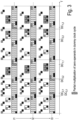
- Figs 3 shows a diagram illustrating three iterations I1 to I3 of modified main loop operation sequences in accordance with an embodiment of the present invention.
- the illustration of Fig. 3 is based on that of Fig. 2 , and thus uses the same sequence of operations.
- the different iterations are manifestations of the control operation of the controller 20 according to the control method of the present invention, which determines dummy clock cycle positions and adds further partial multiplications of zero-operands at the dummy clock cycle positions in the respective main loop iterations, as will be explained in the following in more detail.
- the controller is configured to determine, for each iteration I1 to I3 of the exemplary main loop operation sequence that was illustrated in Fig. 2 , a respective set of respective dummy clock cycle positions.
- a respective set of respective dummy clock cycle positions In the exemplary embodiment of Fig. 3 , in each shown main loop iteration, two dummy clock cycle positions are determined. They are marked graphically on the time axis T by ""DC. For instance, the label DC 1,1 indicates a first dummy clock cycle position within the first iteration 11, and DC 1,2 indicates a second dummy clock cycle position within the first iteration 11. Clock cycles corresponding to the dummy clock cycle positions are indicated as black and white hashing in the respective rectangles.
- the controller is further configured to control the field multiplier block 12 to perform a partial multiplication of zero-operands in these dummy clock cycles corresponding to the determined dummy clock cycle positions.
- These operations are represented in Fig. 3 by large rectangles with a bold diagonal hatching.
- these dummy clock cycles add to the total number of clock cycles required for performing the main loop.
- the dummy clock cycles are additional operations within each main loop iteration and increase the total number of clock cycles
- the number of the dummy wait clock cycles within the processing of a key bit value i.e. within each main loop iteration, can thus be chosen to be constant.
- the same number of dummy clock cycle positions (namely: two) is determined for each of the main loop iterations I1 to I3. This way, the number of clock cycles in each iteration remains fixed.
- the dummy clock cycle positions are different over the different iterations.
- at least two of the sets of dummy clock cycle positions are different from each other.
- the three sets of dummy clock cycle positions underlying the main loop iterations I1, I2 and I3 all differ from each other.
- each two of the dummy clock cycle positions within a given main loop iteration I1, I2, or I3 are determined by the controller to be separated from each other by at least one clock cycle of performing a partial multiplication of non-zero operands because only a single dummy partial multiplication of zero-operands has a hiding effect. This way, the processing of each key bit can require the same amount of time, but the addressing processes will not occur at equal times within the time frames of the respective main loop executions, i.e. they will be shifted from each other.
- the additional dummy partial multiplication of zero-operands do not change the output value of the field multiplier block with respect to an ongoing calculation.
- the field multiplier block consumes additional energy that is advantageously used as noise, to hide the small differences in energy consumption caused by key-dependent addressing of the blocks.
- Figs 4 shows another diagram illustrating three iterations I1 to I3 of modified main loop operation sequences in accordance with another embodiment of the present invention.
- the illustration of Fig. 4 is again based on that of Fig. 2 , and thus uses the same sequence of operations requiring.
- the different iterations I1 to I3 are manifestations of the control operation of the controller 20 according to another embodiment of the control method of the present invention, which determines dummy clock cycle positions and adds further partial multiplications of zero-operands at the dummy clock cycle positions in the respective main loop iterations.
- the controller again determines dummy clock cycle positions, the number of dummy clock cycle positions in each main loop iteration is allowed to be different from that used in other main loop iterations. Some iterations may have equal numbers of dummy clock cycle positions, but not all.
- the first iteration 11 has one dummy clock cycle position
- the second iteration I2 has two
- the third iteration I3 has three dummy clock cycle positions.
- the numbers can be exchanged to form different embodiments, and the numbers can all be different from the present exemplary embodiment.
- This embodiment can therefore further de-synchronize the key dependent addressing of the one or more computational blocks and registers in the main loop iterations and reduce this way the success of the attacks.
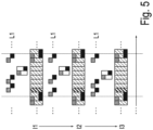
- Fig. 5 shows a further diagram with three variants of operations in the course of performing an individual field multiplication during three different iterations.
- the variation concept presented with reference to Fig. 5 is suited for use with any of the embodiments described herein, and is in particular suitable for the embodiments disclosed with reference to Figs. 3 and 4 .
- the illustrative examples shown in Fig. 5 are based on the operations performed during the second field multiplication during the second iteration L2 shown in Fig. 3 .
- this individual field multiplication is shown in the context of an iteration L1 in the present embodiment.
- this field multiplication operation is varied in that some register operations associated respectively with writing to the BUS and reading from the BUS are shifted to different clock cycles, as shown in the respective lane L1 in the different iterations L1 to L3.
- the time shifts shown in Fig. 5 are exemplary options, other time shifts can be made if it does not influence the correctness of the results. While the shift in time in the performance of these operations does not have any influence on the calculation, at least in the case shown in Fig. 5 , the pattern of performed register operations is further blurred by the irregularity introduced by these time shifts.
- embodiments of a device for performing accelerated elliptic curve point multiplication determine for each of the iterations of a main loop operation sequence a respective set of respective dummy clock cycle positions, and control computational blocks to perform a partial multiplication of zero-operands in dummy clock cycles corresponding to the respective determined dummy clock cycle positions of the set of dummy clock cycle positions for the respective main loop iteration. For any of the sets that has two or more dummy clock cycle positions within the same main loop iteration, each two of the dummy clock cycle positions are separated from each other by at least one clock cycle of performing a partial multiplication of non-zero operands, and at least two of the sets of the dummy clock cycle positions differ from each other.
Landscapes
- Engineering & Computer Science (AREA)
- Computer Security & Cryptography (AREA)
- Computer Networks & Wireless Communication (AREA)
- Signal Processing (AREA)
- Complex Calculations (AREA)
Claims (13)
- Vorrichtung zur Durchführung einer beschleunigten elliptischen Kurven, EC, Punktmultiplikation , umfassend:- einen oder mehrere Rechenblöcke zur Durchführung einer Feldmultiplikation, einer Feldaddition, einer Feldsubtraktion oder einer Feldquadrierung;- adressierbare Register;- einen Bus für den Datenaustausch zwischen den Blöcken und den Registern; und- einen Controller, der konfiguriert istden Betrieb der Rechenblöcke, der Register und des Busses bei der Bestimmung eines EC-Punkt-Multiplikationsergebnisses zu steuern, indem Iterationen einer Hauptschleifenoperationssequenz durchgeführt werden, die Folgendes umfasst- gemäß einem implementierten Feldmultiplikationsalgorithmus: eine sequentielle Berechnung von aus Eingangsmultiplikanden abgeleiteten Teilprodukten und eine Akkumulation der Teilprodukte in einem internen Akkumulationsregister des Rechenblocks zur Bestimmung des Feldprodukts der Eingangsmultiplikanden; und in- Lese- und Schreibzugriffe auf die Register im Zusammenhang mit der Berechnung von Feldmultiplikationen, Feldadditionen und/oder Feldsubtraktionen, und/oder Feldquadrierungen der jeweiligen Operanden;wobei der Controller weiterhin konfiguriert istfür jede der Iterationen der Hauptschleifenoperationssequenz einen jeweiligen Satz von jeweiligen Dummy-Taktzykluspositionen zu bestimmen und die Rechenblöcke zu steuern, um eine Teilmultiplikation von Null-Operanden in Dummy-Taktzyklen durchzuführen, die dem jeweiligen bestimmten Satz von jeweiligen Dummy-Taktzykluspositionen für die jeweilige Hauptschleifeniteration entsprechen, wobei für jeden der Sätze, der zwei oder mehr Dummy-Taktzykluspositionen innerhalb derselben Hauptschleifeniteration aufweist, alle jeweils zwei der Dummy-Taktzykluspositionen durch mindestens einen Taktzyklus der Durchführung einer Teilmultiplikation von Nicht-Null-Operanden voneinander getrennt sind, und wobei sich mindestens zwei der Sätze der Dummy-Taktzykluspositionen voneinander unterscheiden.
- Vorrichtung nach Anspruch 1, wobei der Controller so konfiguriert ist, dass er den Betrieb eines oder mehrerer der Rechenblöcke zur Durchführung von Feldmultiplikation, Feldaddition und/oder Feldsubtraktion und/oder Feldquadrierung sowie die Adressierung der Register so steuert, dass sie während eines oder mehrerer der Dummy-Taktzyklen pausieren.
- Vorrichtung nach Anspruch 1 oder 2, wobei der Controller so konfiguriert ist, dass er die Sätze von Dummy-Taktzykluspositionen unter Verwendung von aktuell in einem oder mehreren Registern gespeicherten Werten bestimmt.
- Vorrichtung nach einem der Ansprüche 1 bis 3, wobei der Controller so konfiguriert ist, dass er die Sätze von Dummy-Taktzykluspositionen unter Verwendung einer von einem Zufallszahlengenerator empfangenen Ausgabe bestimmt.
- Vorrichtung nach einem der Ansprüche 1 bis 4, wobei der Controller so konfiguriert ist, dass er die Sätze von Dummy-Taktzykluspositionen unter Verwendung einer mathematischen Funktion bestimmt, die auf einen aktuellen Wert einer vorbestimmten Größe angewendet wird.
- Vorrichtung nach einem der vorhergehenden Ansprüche, wobei der Controller so konfiguriert ist, dass er mindestens zwei Sätze von Dummy-Taktzykluspositionen mit einer unterschiedlichen Anzahl von Dummy-Taktzykluspositionen bestimmt.
- Vorrichtung nach einem der Ansprüche 1 bis 6, wobei der Controller so konfiguriert ist, dass er die Sätze von Dummy-Taktzykluspositionen bestimmt, die alle eine gleiche Anzahl von Dummy-Taktzykluspositionen aufweisen, wobei mindestens zwei der Sätze unterschiedlich sind.
- Vorrichtung nach einem der vorhergehenden Ansprüche, wobei der Bus als Multiplexer implementiert ist.
- Vorrichtung nach einem der vorhergehenden Ansprüche, die logische Gatter umfasst, die so konfiguriert sind, dass sie auf eine von dem Controller empfangene Operation und Adresse reagieren, einschließlich einer Write-to-BUS-Operation, die einen Ausgang eines Quellblocks mit den Eingängen aller anderen Blöcke verbindet, und einer Read-from-BUS-Operation, bei der nur ein Zielblock Werte an seinem Eingang als Daten zur Verarbeitung annimmt.
- Vorrichtung nach einem der vorhergehenden Ansprüche, wobei der Feldmultiplikatorblock so konfiguriert ist, dass er die Feldmultiplikationsoperation gemäß einer Implementierung einer Montgomery-Leiters oder eines Double-and-Add- oder eines anderen binären kP-Ausführungsalgorithmus durchführt.
- Kryptografische Vorrichtung, die so konfiguriert ist, dass sie eine Verschlüsselung oder Entschlüsselung von empfangenen Eingabedaten oder eine Erzeugung oder Überprüfung einer digitalen Signatur oder einen Authentifizierungsprozess unter Verwendung von kryptografischen Operationen mit elliptischen Kurven über einem endlichen Feld durchführt, wobei die kryptografische Vorrichtung eine Vorrichtung nach einem der Ansprüche 1 bis 10 umfasst.
- Verfahren zur Steuerung des Betriebs einer Vorrichtung zur Durchführung einer beschleunigten elliptischen Kurven, EC, Punktmultiplikation, umfassend- Steuern des Betriebs von Rechenblöcken, Registern und eines Busses bei der Bestimmung eines EC-Punkt-Multiplikationsergebnisses durch die Durchführung von Iterationen einer Hauptschleifenoperationssequenz, die Folgendes umfasstwobei das Steuern ferner Folgendes umfasst- gemäß einem implementierten Feldmultiplikationsalgorithmus: eine sequentielle Berechnung von Teilprodukten, die von Eingangsmultiplikanden abgeleitet sind, und eine Akkumulation der Teilprodukte in einem Akkumulationsregister zur Bestimmung des Feldprodukts der Eingangsmultiplikanden; und in- Lese- und Schreibzugriffe auf die Register im Zusammenhang mit der Berechnung von Feldmultiplikationen, Feldadditionen und/oder Feldsubtraktionen und/oder Feldquadrierungen der jeweiligen Operanden;- Bestimmen eines jeweiligen Satzes von jeweiligen Dummy-Taktzykluspositionen, d.h. eines Satzes von Dummy-Taktzykluspositionen, für jede der Iterationen der Hauptschleifenoperationssequenz,- Steuern der Rechenblöcke, um eine Teilmultiplikation von Null-Operanden in Dummy-Taktzyklen durchzuführen, die dem jeweiligen bestimmten Satz von jeweiligen Dummy-Taktzykluspositionen für die jeweilige Hauptschleifeniteration entsprechen, wobei,- für jede der Mengen, die zwei oder mehr Dummy-Taktzykluspositionen innerhalb dergleichen Hauptschleifeniteration aufweist, alle jeweils zwei der Dummy-Taktzykluspositionen durch mindestens einen Taktzyklus der Durchführung einer Teilmultiplikation von Nicht-Null-Operanden voneinander getrennt sind, und- wobei sich mindestens zwei der Sätze von Dummy-Taktzykluspositionen voneinander unterscheiden.
- Computerprogramm mit ausführbarem Programmcode, der, wenn er in einem Speicher eines programmierbaren Computers gespeichert ist, den Computer anweist, das Verfahren nach Anspruch 12 durchzuführen.
Applications Claiming Priority (1)
| Application Number | Priority Date | Filing Date | Title |
|---|---|---|---|
| EP21217968 | 2021-12-28 |
Publications (3)
| Publication Number | Publication Date |
|---|---|
| EP4207672A1 EP4207672A1 (de) | 2023-07-05 |
| EP4207672C0 EP4207672C0 (de) | 2024-04-17 |
| EP4207672B1 true EP4207672B1 (de) | 2024-04-17 |
Family
ID=79185688
Family Applications (1)
| Application Number | Title | Priority Date | Filing Date |
|---|---|---|---|
| EP22168962.3A Active EP4207672B1 (de) | 2021-12-28 | 2022-04-20 | Dummy-teilmultiplikation von null-operanden als kostengünstiges mittel zur reduzierung des erfolgs von sca-angriffen gegen ecc |
Country Status (1)
| Country | Link |
|---|---|
| EP (1) | EP4207672B1 (de) |
-
2022
- 2022-04-20 EP EP22168962.3A patent/EP4207672B1/de active Active
Also Published As
| Publication number | Publication date |
|---|---|
| EP4207672C0 (de) | 2024-04-17 |
| EP4207672A1 (de) | 2023-07-05 |
Similar Documents
| Publication | Publication Date | Title |
|---|---|---|
| May et al. | Non-deterministic processors | |
| US10635405B2 (en) | Homogenous atomic pattern for double, add, and subtract operations for digital authentication using elliptic curve cryptography | |
| KR100568393B1 (ko) | 암호화 프로세서 | |
| CN107040362B (zh) | 模乘设备和方法 | |
| Yen et al. | Power analysis by exploiting chosen message and internal collisions–vulnerability of checking mechanism for RSA-decryption | |
| US8391477B2 (en) | Cryptographic device having tamper resistance to power analysis attack | |
| Giraud et al. | Atomicity improvement for elliptic curve scalar multiplication | |
| KR102132261B1 (ko) | 비교 연산이 필요없이 최종 모듈러 감소를 하는 몽고메리 곱셈 방법 및 곱셈기 | |
| JP5182364B2 (ja) | サイドチャネル攻撃に対する耐タンパ性を有する暗号処理方法 | |
| CN103903047A (zh) | 一种适用于rfid安全通信的椭圆曲线加密协处理器 | |
| Guajardo et al. | Efficient implementation of elliptic curve cryptosystems on the TI MSP430x33x family of microcontrollers | |
| CN108108614A (zh) | 安全处理器以及安全处理器的操作方法 | |
| KR101925868B1 (ko) | 모듈러 계산 유닛 및 그것을 포함하는 보안 시스템 | |
| CA2775325A1 (en) | Modular exponentiation method and device resistant against side-channel attacks | |
| Hutter et al. | A cryptographic processor for low-resource devices: Canning ECDSA and AES like sardines | |
| US20100183142A1 (en) | Encryption Processing Apparatus, Encryption Processing Method, and Computer Program | |
| Bertoni et al. | Power aware design of an elliptic curve coprocessor for 8 bit platforms | |
| Clavier et al. | Square always exponentiation | |
| EP4207672A1 (de) | Dummy-teilmultiplikation von null-operanden als kostengünstiges mittel zur reduzierung des erfolgs von sca-angriffen gegen ecc | |
| Liu et al. | Energy-efficient elliptic curve cryptography for MSP430-based wireless sensor nodes | |
| Fournaris | Fault and power analysis attack protection techniques for standardized public key cryptosystems | |
| JP3878853B2 (ja) | 公開鍵暗号アルゴリズムを用いる電子構成品におけるモジュラべき乗演算アルゴリズム | |
| Piacentini et al. | An Unprofiled Single Trace Side-Channel Attack for Asymmetric Cryptosystems | |
| US20240111908A1 (en) | Cryptographic hardware accelerator with dummy block addressing for protection against side channel attacks | |
| KR20190022023A (ko) | 하드웨어 구현된 모듈러 역원 모듈 |
Legal Events
| Date | Code | Title | Description |
|---|---|---|---|
| PUAI | Public reference made under article 153(3) epc to a published international application that has entered the european phase |
Free format text: ORIGINAL CODE: 0009012 |
|
| STAA | Information on the status of an ep patent application or granted ep patent |
Free format text: STATUS: THE APPLICATION HAS BEEN PUBLISHED |
|
| AK | Designated contracting states |
Kind code of ref document: A1 Designated state(s): AL AT BE BG CH CY CZ DE DK EE ES FI FR GB GR HR HU IE IS IT LI LT LU LV MC MK MT NL NO PL PT RO RS SE SI SK SM TR |
|
| STAA | Information on the status of an ep patent application or granted ep patent |
Free format text: STATUS: REQUEST FOR EXAMINATION WAS MADE |
|
| 17P | Request for examination filed |
Effective date: 20230829 |
|
| RBV | Designated contracting states (corrected) |
Designated state(s): AL AT BE BG CH CY CZ DE DK EE ES FI FR GB GR HR HU IE IS IT LI LT LU LV MC MK MT NL NO PL PT RO RS SE SI SK SM TR |
|
| GRAP | Despatch of communication of intention to grant a patent |
Free format text: ORIGINAL CODE: EPIDOSNIGR1 |
|
| STAA | Information on the status of an ep patent application or granted ep patent |
Free format text: STATUS: GRANT OF PATENT IS INTENDED |
|
| RIC1 | Information provided on ipc code assigned before grant |
Ipc: H04L 9/30 20060101ALI20231019BHEP Ipc: H04L 9/00 20220101AFI20231019BHEP |
|
| INTG | Intention to grant announced |
Effective date: 20231108 |
|
| GRAS | Grant fee paid |
Free format text: ORIGINAL CODE: EPIDOSNIGR3 |
|
| GRAA | (expected) grant |
Free format text: ORIGINAL CODE: 0009210 |
|
| STAA | Information on the status of an ep patent application or granted ep patent |
Free format text: STATUS: THE PATENT HAS BEEN GRANTED |
|
| AK | Designated contracting states |
Kind code of ref document: B1 Designated state(s): AL AT BE BG CH CY CZ DE DK EE ES FI FR GB GR HR HU IE IS IT LI LT LU LV MC MK MT NL NO PL PT RO RS SE SI SK SM TR |
|
| REG | Reference to a national code |
Ref country code: GB Ref legal event code: FG4D |
|
| REG | Reference to a national code |
Ref country code: CH Ref legal event code: EP |
|
| REG | Reference to a national code |
Ref country code: DE Ref legal event code: R096 Ref document number: 602022002862 Country of ref document: DE |
|
| REG | Reference to a national code |
Ref country code: IE Ref legal event code: FG4D |
|
| U01 | Request for unitary effect filed |
Effective date: 20240517 |
|
| U07 | Unitary effect registered |
Designated state(s): AT BE BG DE DK EE FI FR IT LT LU LV MT NL PT SE SI Effective date: 20240527 |
|
| U20 | Renewal fee for the european patent with unitary effect paid |
Year of fee payment: 3 Effective date: 20240527 |
|
| PG25 | Lapsed in a contracting state [announced via postgrant information from national office to epo] |
Ref country code: IS Free format text: LAPSE BECAUSE OF FAILURE TO SUBMIT A TRANSLATION OF THE DESCRIPTION OR TO PAY THE FEE WITHIN THE PRESCRIBED TIME-LIMIT Effective date: 20240817 |
|
| PG25 | Lapsed in a contracting state [announced via postgrant information from national office to epo] |
Ref country code: HR Free format text: LAPSE BECAUSE OF FAILURE TO SUBMIT A TRANSLATION OF THE DESCRIPTION OR TO PAY THE FEE WITHIN THE PRESCRIBED TIME-LIMIT Effective date: 20240417 |
|
| PG25 | Lapsed in a contracting state [announced via postgrant information from national office to epo] |
Ref country code: GR Free format text: LAPSE BECAUSE OF FAILURE TO SUBMIT A TRANSLATION OF THE DESCRIPTION OR TO PAY THE FEE WITHIN THE PRESCRIBED TIME-LIMIT Effective date: 20240718 |
|
| PG25 | Lapsed in a contracting state [announced via postgrant information from national office to epo] |
Ref country code: ES Free format text: LAPSE BECAUSE OF FAILURE TO SUBMIT A TRANSLATION OF THE DESCRIPTION OR TO PAY THE FEE WITHIN THE PRESCRIBED TIME-LIMIT Effective date: 20240417 |
|
| PG25 | Lapsed in a contracting state [announced via postgrant information from national office to epo] |
Ref country code: PL Free format text: LAPSE BECAUSE OF FAILURE TO SUBMIT A TRANSLATION OF THE DESCRIPTION OR TO PAY THE FEE WITHIN THE PRESCRIBED TIME-LIMIT Effective date: 20240417 |
|
| PG25 | Lapsed in a contracting state [announced via postgrant information from national office to epo] |
Ref country code: PL Free format text: LAPSE BECAUSE OF FAILURE TO SUBMIT A TRANSLATION OF THE DESCRIPTION OR TO PAY THE FEE WITHIN THE PRESCRIBED TIME-LIMIT Effective date: 20240417 Ref country code: NO Free format text: LAPSE BECAUSE OF FAILURE TO SUBMIT A TRANSLATION OF THE DESCRIPTION OR TO PAY THE FEE WITHIN THE PRESCRIBED TIME-LIMIT Effective date: 20240717 Ref country code: IS Free format text: LAPSE BECAUSE OF FAILURE TO SUBMIT A TRANSLATION OF THE DESCRIPTION OR TO PAY THE FEE WITHIN THE PRESCRIBED TIME-LIMIT Effective date: 20240817 Ref country code: HR Free format text: LAPSE BECAUSE OF FAILURE TO SUBMIT A TRANSLATION OF THE DESCRIPTION OR TO PAY THE FEE WITHIN THE PRESCRIBED TIME-LIMIT Effective date: 20240417 Ref country code: GR Free format text: LAPSE BECAUSE OF FAILURE TO SUBMIT A TRANSLATION OF THE DESCRIPTION OR TO PAY THE FEE WITHIN THE PRESCRIBED TIME-LIMIT Effective date: 20240718 Ref country code: ES Free format text: LAPSE BECAUSE OF FAILURE TO SUBMIT A TRANSLATION OF THE DESCRIPTION OR TO PAY THE FEE WITHIN THE PRESCRIBED TIME-LIMIT Effective date: 20240417 Ref country code: RS Free format text: LAPSE BECAUSE OF FAILURE TO SUBMIT A TRANSLATION OF THE DESCRIPTION OR TO PAY THE FEE WITHIN THE PRESCRIBED TIME-LIMIT Effective date: 20240717 |
|
| REG | Reference to a national code |
Ref country code: DE Ref legal event code: R097 Ref document number: 602022002862 Country of ref document: DE |
|
| PG25 | Lapsed in a contracting state [announced via postgrant information from national office to epo] |
Ref country code: CZ Free format text: LAPSE BECAUSE OF FAILURE TO SUBMIT A TRANSLATION OF THE DESCRIPTION OR TO PAY THE FEE WITHIN THE PRESCRIBED TIME-LIMIT Effective date: 20240417 |
|
| PG25 | Lapsed in a contracting state [announced via postgrant information from national office to epo] |
Ref country code: SK Free format text: LAPSE BECAUSE OF FAILURE TO SUBMIT A TRANSLATION OF THE DESCRIPTION OR TO PAY THE FEE WITHIN THE PRESCRIBED TIME-LIMIT Effective date: 20240417 Ref country code: RO Free format text: LAPSE BECAUSE OF FAILURE TO SUBMIT A TRANSLATION OF THE DESCRIPTION OR TO PAY THE FEE WITHIN THE PRESCRIBED TIME-LIMIT Effective date: 20240417 |
|
| PG25 | Lapsed in a contracting state [announced via postgrant information from national office to epo] |
Ref country code: SM Free format text: LAPSE BECAUSE OF FAILURE TO SUBMIT A TRANSLATION OF THE DESCRIPTION OR TO PAY THE FEE WITHIN THE PRESCRIBED TIME-LIMIT Effective date: 20240417 |
|
| PG25 | Lapsed in a contracting state [announced via postgrant information from national office to epo] |
Ref country code: SM Free format text: LAPSE BECAUSE OF FAILURE TO SUBMIT A TRANSLATION OF THE DESCRIPTION OR TO PAY THE FEE WITHIN THE PRESCRIBED TIME-LIMIT Effective date: 20240417 Ref country code: SK Free format text: LAPSE BECAUSE OF FAILURE TO SUBMIT A TRANSLATION OF THE DESCRIPTION OR TO PAY THE FEE WITHIN THE PRESCRIBED TIME-LIMIT Effective date: 20240417 Ref country code: RO Free format text: LAPSE BECAUSE OF FAILURE TO SUBMIT A TRANSLATION OF THE DESCRIPTION OR TO PAY THE FEE WITHIN THE PRESCRIBED TIME-LIMIT Effective date: 20240417 Ref country code: CZ Free format text: LAPSE BECAUSE OF FAILURE TO SUBMIT A TRANSLATION OF THE DESCRIPTION OR TO PAY THE FEE WITHIN THE PRESCRIBED TIME-LIMIT Effective date: 20240417 Ref country code: MC Free format text: LAPSE BECAUSE OF FAILURE TO SUBMIT A TRANSLATION OF THE DESCRIPTION OR TO PAY THE FEE WITHIN THE PRESCRIBED TIME-LIMIT Effective date: 20240417 |
|
| PLBE | No opposition filed within time limit |
Free format text: ORIGINAL CODE: 0009261 |
|
| STAA | Information on the status of an ep patent application or granted ep patent |
Free format text: STATUS: NO OPPOSITION FILED WITHIN TIME LIMIT |
|
| 26N | No opposition filed |
Effective date: 20250120 |
|
| U20 | Renewal fee for the european patent with unitary effect paid |
Year of fee payment: 4 Effective date: 20250303 |
|
| PG25 | Lapsed in a contracting state [announced via postgrant information from national office to epo] |
Ref country code: IE Free format text: LAPSE BECAUSE OF NON-PAYMENT OF DUE FEES Effective date: 20240420 |
|
| PG25 | Lapsed in a contracting state [announced via postgrant information from national office to epo] |
Ref country code: CY Free format text: LAPSE BECAUSE OF FAILURE TO SUBMIT A TRANSLATION OF THE DESCRIPTION OR TO PAY THE FEE WITHIN THE PRESCRIBED TIME-LIMIT; INVALID AB INITIO Effective date: 20220420 |
|
| PG25 | Lapsed in a contracting state [announced via postgrant information from national office to epo] |
Ref country code: HU Free format text: LAPSE BECAUSE OF FAILURE TO SUBMIT A TRANSLATION OF THE DESCRIPTION OR TO PAY THE FEE WITHIN THE PRESCRIBED TIME-LIMIT; INVALID AB INITIO Effective date: 20220420 |
|
| REG | Reference to a national code |
Ref country code: CH Ref legal event code: H13 Free format text: ST27 STATUS EVENT CODE: U-0-0-H10-H13 (AS PROVIDED BY THE NATIONAL OFFICE) Effective date: 20251125 |
|
| PG25 | Lapsed in a contracting state [announced via postgrant information from national office to epo] |
Ref country code: CH Free format text: LAPSE BECAUSE OF NON-PAYMENT OF DUE FEES Effective date: 20250430 |
|
| U20 | Renewal fee for the european patent with unitary effect paid |
Year of fee payment: 5 Effective date: 20260311 |