EP4207604A1 - Analog to digital converter apparatus with time continuous input and corresponding method - Google Patents
Analog to digital converter apparatus with time continuous input and corresponding method Download PDFInfo
- Publication number
- EP4207604A1 EP4207604A1 EP22211363.1A EP22211363A EP4207604A1 EP 4207604 A1 EP4207604 A1 EP 4207604A1 EP 22211363 A EP22211363 A EP 22211363A EP 4207604 A1 EP4207604 A1 EP 4207604A1
- Authority
- EP
- European Patent Office
- Prior art keywords
- digital
- analog
- output
- input
- conversion
- Prior art date
- Legal status (The legal status is an assumption and is not a legal conclusion. Google has not performed a legal analysis and makes no representation as to the accuracy of the status listed.)
- Withdrawn
Links
Images


Classifications
-
- H—ELECTRICITY
- H03—ELECTRONIC CIRCUITRY
- H03M—CODING; DECODING; CODE CONVERSION IN GENERAL
- H03M1/00—Analogue/digital conversion; Digital/analogue conversion
- H03M1/12—Analogue/digital converters
- H03M1/34—Analogue value compared with reference values
- H03M1/36—Analogue value compared with reference values simultaneously only, i.e. parallel type
-
- H—ELECTRICITY
- H03—ELECTRONIC CIRCUITRY
- H03M—CODING; DECODING; CODE CONVERSION IN GENERAL
- H03M3/00—Conversion of analogue values to or from differential modulation
- H03M3/30—Delta-sigma modulation
- H03M3/39—Structural details of delta-sigma modulators, e.g. incremental delta-sigma modulators
- H03M3/412—Structural details of delta-sigma modulators, e.g. incremental delta-sigma modulators characterised by the number of quantisers and their type and resolution
- H03M3/422—Structural details of delta-sigma modulators, e.g. incremental delta-sigma modulators characterised by the number of quantisers and their type and resolution having one quantiser only
- H03M3/424—Structural details of delta-sigma modulators, e.g. incremental delta-sigma modulators characterised by the number of quantisers and their type and resolution having one quantiser only the quantiser being a multiple bit one
-
- G—PHYSICS
- G01—MEASURING; TESTING
- G01S—RADIO DIRECTION-FINDING; RADIO NAVIGATION; DETERMINING DISTANCE OR VELOCITY BY USE OF RADIO WAVES; LOCATING OR PRESENCE-DETECTING BY USE OF THE REFLECTION OR RERADIATION OF RADIO WAVES; ANALOGOUS ARRANGEMENTS USING OTHER WAVES
- G01S7/00—Details of systems according to groups G01S13/00, G01S15/00, G01S17/00
- G01S7/52—Details of systems according to groups G01S13/00, G01S15/00, G01S17/00 of systems according to group G01S15/00
- G01S7/523—Details of pulse systems
- G01S7/526—Receivers
-
- H—ELECTRICITY
- H03—ELECTRONIC CIRCUITRY
- H03M—CODING; DECODING; CODE CONVERSION IN GENERAL
- H03M1/00—Analogue/digital conversion; Digital/analogue conversion
- H03M1/12—Analogue/digital converters
- H03M1/18—Automatic control for modifying the range of signals the converter can handle, e.g. gain ranging
- H03M1/181—Automatic control for modifying the range of signals the converter can handle, e.g. gain ranging in feedback mode, i.e. by determining the range to be selected from one or more previous digital output values
-
- H—ELECTRICITY
- H03—ELECTRONIC CIRCUITRY
- H03M—CODING; DECODING; CODE CONVERSION IN GENERAL
- H03M1/00—Analogue/digital conversion; Digital/analogue conversion
- H03M1/12—Analogue/digital converters
- H03M1/34—Analogue value compared with reference values
- H03M1/36—Analogue value compared with reference values simultaneously only, i.e. parallel type
- H03M1/361—Analogue value compared with reference values simultaneously only, i.e. parallel type having a separate comparator and reference value for each quantisation level, i.e. full flash converter type
-
- H—ELECTRICITY
- H03—ELECTRONIC CIRCUITRY
- H03M—CODING; DECODING; CODE CONVERSION IN GENERAL
- H03M1/00—Analogue/digital conversion; Digital/analogue conversion
- H03M1/12—Analogue/digital converters
- H03M1/34—Analogue value compared with reference values
- H03M1/36—Analogue value compared with reference values simultaneously only, i.e. parallel type
- H03M1/367—Non-linear conversion
-
- H—ELECTRICITY
- H03—ELECTRONIC CIRCUITRY
- H03M—CODING; DECODING; CODE CONVERSION IN GENERAL
- H03M3/00—Conversion of analogue values to or from differential modulation
- H03M3/30—Delta-sigma modulation
- H03M3/458—Analogue/digital converters using delta-sigma modulation as an intermediate step
- H03M3/476—Non-linear conversion systems
-
- G—PHYSICS
- G01—MEASURING; TESTING
- G01S—RADIO DIRECTION-FINDING; RADIO NAVIGATION; DETERMINING DISTANCE OR VELOCITY BY USE OF RADIO WAVES; LOCATING OR PRESENCE-DETECTING BY USE OF THE REFLECTION OR RERADIATION OF RADIO WAVES; ANALOGOUS ARRANGEMENTS USING OTHER WAVES
- G01S15/00—Systems using the reflection or reradiation of acoustic waves, e.g. sonar systems
- G01S15/02—Systems using the reflection or reradiation of acoustic waves, e.g. sonar systems using reflection of acoustic waves
- G01S15/06—Systems determining the position data of a target
- G01S15/08—Systems for measuring distance only
- G01S15/10—Systems for measuring distance only using transmission of interrupted, pulse-modulated waves
Definitions
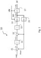
- FIG 1 it is shown instead a block schematization as a loop of a second order sigma delta analog to digital converter apparatus 10, in which an analog input differential signal, in particular an input differential voltage Vdiff, which is time continuous, is brought as input of a difference block 21, which receives a feedback signal, in particular, a feedback voltage Vfeed, outputting an error voltage Ev.
- the error voltage Ev is supplied to a first analog integrator 11, implementing an integration function, e.g. 1/s in the Laplace transform representation.
- the output of such analog integrator 11 is brought as input of a second difference block 22, which receives also the feedback voltage Vfeed, outputting a second error voltage Ev2.
- Target performances which may be reached with this loop are 15bit resolution, 20MHz clock, 100Khz bandwidth
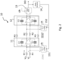
- figure 2 is shown a more detailed possible implementation of a Sigma Delta ADC 10 after the general schematics of figure 1 , with a differential structure is shown.
- Differential positive and negative input analog voltages Vi+ and Vi- which together form the differential voltage V diff , and which are time continuous, are brought to positive and negative branches inputs of the ADC 10 which include each a resistor R1 in series with the input, in which flows input analog currents i+ and i-.
- the integrator 11 is implemented by a first differential amplifier with a capacitive feedback, which has its positive and negative inputs coupled to the positive and negative input voltages Vi+ and Vi-, i.e. receiving the input analog currents i+ and i-, through the resistors R1, while its differential outputs are coupled, through second resistors R2 in series, to the corresponding differential inputs of the second integrator 12, also implemented by a differential amplifier with a capacitive feedback.
- the amplifiers 11 and 12 embody together a two-stage analog amplifier.
- Feedback resistors R3 couple the negative output of the second amplifier 12 with the positive input of the first amplifier 11 and the positive output of the second amplifier 12 with the negative input of the first amplifier 11.
- Both the amplifier 11 and 12 have feedback capacitors, implementing the capacitive feedback, coupling their outputs to their inputs of corresponding polarity, i.e. two capacitors C1 for amplifier 11 and two capacitors C2 for amplifier 12.
- the outputs of the second amplifier 12 as coupled to the inputs of corresponding polarity of a flash ADC 13, which is clocked by a clock signal clk, supplying a digital output DO, which is also applied to a DWA (Data Weighted Averaging) Scrambler 14, which shapes the noise in the digital output and which digital output supplies a first DAC 151 and a second digital DAC 152, i.e. the function of DAC 15 is implemented by two parallel DAC, clocked by the clock signal clk, which differential analog outputs, differential currents i1 and i2 respectively, are coupled to the input of opposite polarity of the first differential amplifier 11 and second differential amplifier 12, respectively.
- DWA Data Weighted Averaging
- the difference blocks 21, 22 are obtained just by the common nodes in which the currents from the resistors R1 and R2 and from the DAC 151 and 152 are injected, which sum currents with opposite polarity.
- the DAC 151 and 152 perform the multibit feedback in the ADC 10.
- the ADC 10 samples on the falling edge of the clock signal clk, while the DACs 151, 152 are on during the interval in which the clock signal clk is high.
- the digital low pass filter 17 is not shown in Figure 2 .
- the present disclosure provides solutions regarding an analog to digital converter apparatus, adapt to receive a continuous input signal
- said flash ADC converter has a digital output which quantized values are represented with a given number of bits and said flash ADC converter comprises a number of comparators with respective different thresholds covering the range of the flash ADC converter input signal which is less than two to the power of said number of bits, in particular said given number of bits being 10 and said number of comparators being 17.
- said flash ADC conversion is configured to implement a conversion characteristic from analog input voltage to digital code output where the resolution of the quantized values in the digital code output varies exponentially.
- said integrating block comprise a first integrating stage and a second integrating stage in series, said feedback path comprising a digital to analog conversion block comprising a first digital to analog converter, receiving as input said digital output of said flash analog to digital converter, which is compared at least to the input signal to obtain an error signal which is brought as input to said first integrating stage, and second digital to analog converter. receiving as input said digital output of said flash analog to digital converter, which is compared to the output signal of said first integrating stage to obtain a second error signal which is brought as input to said flash analog to digital converter.
- said control block is configured to perform a proportional and integral control and comprises proportional and integral paths, said proportional path applying a proportional constant, in particular equal to two to the power minus two and said number of comparators being in particular 17.
- the present disclosure also provides solutions regarding a method performing analog to digital conversion of a continuous input signal
- said flash ADC conversion includes providing a digital output with a given number of bits and comprises a number of comparators which is less than then two the power of said number of bits, in particular said given number of bits is 10 and said number of comparators is 17.
- flash ADC conversion implements a conversion characteristic from analog input voltage to digital code output which comprises voltage thresholds for the input voltage are increasingly exponentially spaced, in particular exponentially spaced.
- said flash ADC conversion implements a conversion characteristic from analog input voltage to digital code output where the resolution of the quantized values in the digital code output increases, in particular exponentially.
- said control comprises a proportional and integral control on proportional and integral paths, said proportional path applying a proportional constant, in particular equal to two to the power minus two and said number of comparators being in particular 17.
- the 10-bit digital output DO of the PID 34 is also supplied to a digital low pass filter 17 which supplies an output with a greater number of bits, e.g. 15 bits.
- the ADC 33, the PID 34 and the LPF 17 are clocked by a same clock, e.g. 20 MHz.
- the flash ADC 33 has a reduced complexity, using a lesser number of comparators than the two to the number of bits of the output of the flash ADC 33 minus one, in particular in the embodiment shown, only 17 comparators.
- an uncompressed characteristic R and a compressed characteristic B There are shown an uncompressed characteristic R and a compressed characteristic B.
- the abscissa values input signal values
- the quantized codes QC are spaced along the vertical axis, i.e. code values, increasingly spaced going from the origin of the axes toward the positive and negative extremes of the vertical axis, i.e. the maximum and minimum value of the range of the quantized codes QC.
- the thresholds of the comparators which are 17, are spaced exponentially, starting from the origin, i.e. zero volt of input signal, along both the positive and negative horizontal axis representing the input voltage (AVI) of the flash ADC 33.
- the 17 values may be:
- the difference block 21 again is obtained by summing the differential current in the respective output nodes with the feedback signal, which is represented by differential currents IDAC and IDAC , positive and negative.
- the integrator block 11 is carried out by an operational amplifier with feedback capacitors.
- the ADC 33 is embodied by a logarithmic ADC 331 with 17 comparators, CP 1 ...CP 17 , which digital output is supplied to a register 332 applying a z -1 delay function, in order to synchronize the output levels of the ADC 33.
- figure 7 it is shown an embodiment in which, as shown in figure 2 , there are two DAC 351 and 352, which receive the digital output DO as input and output respective currents IDAC and IDAC , coupled, in the manner shown for figure 2 , i.e. to the opposite polarity inputs of the first amplifier 31 and of the ADC 33.
- This introduces some more phase rotation which helps stability.
- Decoupling resistor Rd are indicated between the analog integrator 11 and the ADC 33, in particular of the comparators 331.
- An object 60 at a distance L reflects the ultrasound waves associated to the ultrasound pulse, which are detected by the piezoelectric transducer 52 itself, which output is sent to a receiving circuit 53, which issues a receive control pulse RP to the control circuit CM, which measures the time difference T between the transmit control pulse TP and the receive control pulse RP.
- the time difference T is also known as time of flight and knowing the propagation speed of the ultrasound pulse the distance L can be determined.
- FIG 8B it is shown a partial block schematics of the ultrasound detector of obstacles 50 comprising the transducer 52, schematized as a RC parallel pair, which is driven by the pulse transmitter 51, coupled to it by a transformer.
- the transducer 52 is also is coupled for reception to the ultrasonic sensor receiver 53, which comprises in its turn an ADC converter 30 (in variant embodiments 30').
- an ultrasound received signal RS which is an analog differential signal
- a signal chain comprising a clamp circuit CP, then a low noise amplifier LNA and then a variable gain amplifier VGA, which gain is controlled by the control module CM through a DCA DC1, and which supplies the differential voltage Vdiff to the input of the ADC converter 30.
- the solution described allows to remove the antialiasing filter and to use a flash ADC comparator with a lesser number of comparators by an arrangement which inserts a proportional integral control in the loop after the flash ADC.
Landscapes
- Engineering & Computer Science (AREA)
- Theoretical Computer Science (AREA)
- Physics & Mathematics (AREA)
- Nonlinear Science (AREA)
- Computer Networks & Wireless Communication (AREA)
- General Physics & Mathematics (AREA)
- Radar, Positioning & Navigation (AREA)
- Remote Sensing (AREA)
- Analogue/Digital Conversion (AREA)
Abstract
Description
- Embodiments of the present disclosure relate to techniques for an analog to digital conversion with time continuous input.
- Embodiments of the present disclosure relate in particular to ultrasound detectors for obstacle recognition based on time-of-flight evaluation comprising analog to digital converters, in particular in the receiver.
- The systems which require an analog to digital conversion with high resolution, show problems of DNL (Differential Non Linearity) and INL (Integral Non Linearity), as well harmonic distortion, aliasing. A big area is required in the chip thus for an antialiasing filter integrated and the problems mentioned also determine low accuracy.
- A solution known in the prior art uses a Sigma Delta ADC with time continuous input of the second order and multibit feedback.
- In
figure 1 it is shown instead a block schematization as a loop of a second order sigma delta analog todigital converter apparatus 10, in which an analog input differential signal, in particular an input differential voltage Vdiff, which is time continuous, is brought as input of adifference block 21, which receives a feedback signal, in particular, a feedback voltage Vfeed, outputting an error voltage Ev. The error voltage Ev is supplied to a firstanalog integrator 11, implementing an integration function, e.g. 1/s in the Laplace transform representation. The output of suchanalog integrator 11 is brought as input of asecond difference block 22, which receives also the feedback voltage Vfeed, outputting a second error voltage Ev2. The second error voltage Ev2 is supplied to a secondanalog integrator 12, which output is supplied to aflash ADC 13, a 10 bit flash ADC in the example. A 10 bit digital output DO of theADC 13 is fed back as the analog feedback voltage Vfeed, through aDAC 15 to the difference blocks 21, 22. The 10 bit digital output DO of the ADC 13 is also supplied to a digitallow pass filter 17 which supplies an output DF with a greater number of bits, e.g. 15 bits. The ADC 13 and the digitallow pass filter 17 are clocked by a same clock clk, e.g. 20 MHz. - Target performances which may be reached with this loop are 15bit resolution, 20MHz clock, 100Khz bandwidth
- In
figure 2 is shown a more detailed possible implementation of a Sigma Delta ADC 10 after the general schematics offigure 1 , with a differential structure is shown. - Differential positive and negative input analog voltages Vi+ and Vi-, which together form the differential voltage Vdiff, and which are time continuous, are brought to positive and negative branches inputs of the
ADC 10 which include each a resistor R1 in series with the input, in which flows input analog currents i+ and i-. Theintegrator 11 is implemented by a first differential amplifier with a capacitive feedback, which has its positive and negative inputs coupled to the positive and negative input voltages Vi+ and Vi-, i.e. receiving the input analog currents i+ and i-, through the resistors R1, while its differential outputs are coupled, through second resistors R2 in series, to the corresponding differential inputs of thesecond integrator 12, also implemented by a differential amplifier with a capacitive feedback. Theamplifiers - Feedback resistors R3 couple the negative output of the
second amplifier 12 with the positive input of thefirst amplifier 11 and the positive output of thesecond amplifier 12 with the negative input of thefirst amplifier 11. Both theamplifier amplifier 11 and two capacitors C2 foramplifier 12. - The outputs of the
second amplifier 12 as coupled to the inputs of corresponding polarity of aflash ADC 13, which is clocked by a clock signal clk, supplying a digital output DO, which is also applied to a DWA (Data Weighted Averaging) Scrambler 14, which shapes the noise in the digital output and which digital output supplies afirst DAC 151 and a seconddigital DAC 152, i.e. the function ofDAC 15 is implemented by two parallel DAC, clocked by the clock signal clk, which differential analog outputs, differential currents i1 and i2 respectively, are coupled to the input of opposite polarity of the firstdifferential amplifier 11 and seconddifferential amplifier 12, respectively. In this way the difference blocks 21, 22 are obtained just by the common nodes in which the currents from the resistors R1 and R2 and from theDAC ADC 10 samples on the falling edge of the clock signal clk, while theDACs low pass filter 17 is not shown inFigure 2 . - In the ADC of
Figure 1 ,2 stages feedback DACs - The loop of
Figures 1 ,2 has an important drawback that needs to resolve, the number of comparators required by the flash ADC, i.e. for example a 10bit flash ADC requires 1024 comparators, which occupy a big area on the chip. - On the basis of the foregoing description, the need is felt for solutions which overcome one or more of the previously outlined drawbacks.
- According to one or more embodiments, such an object is achieved through an apparatus having the features specifically set forth in the claims that follow. Embodiments moreover concerns a related method.
- The claims are an integral part of the technical teaching of the disclosure provided herein.
- As mentioned in the foregoing, the present disclosure provides solutions regarding an analog to digital converter apparatus, adapt to receive a continuous input signal,
- comprising an integrating block, comprising at least an integrating stage, which output is coupled to a flash analog to digital converter,
- said analog to digital converter apparatus comprising a feedback path coupled to the output of said flash analog to digital converter, said feedback path comprising at least a digital to analog conversion block which output is compared at least to the input signal to obtain an error signal which is brought as input to said integrating block ,
- wherein a control block, e.g. a controller, configured to perform a control comprising at least a digital integration, is coupled between the output of said flash analog to digital converter and said feedback path.
- In variant embodiments, said flash ADC converter has a digital output which quantized values are represented with a given number of bits and said flash ADC converter comprises a number of comparators with respective different thresholds covering the range of the flash ADC converter input signal which is less than two to the power of said number of bits, in particular said given number of bits being 10 and said number of comparators being 17.
- In variant embodiments, said flash ADC conversion is configured to implement a conversion characteristic from analog input voltage to digital code output which comprise voltage thresholds for the input voltage which are exponentially spaced.
- In variant embodiments, said flash ADC conversion is configured to implement a conversion characteristic from analog input voltage to digital code output where the resolution of the quantized values in the digital code output varies exponentially.
- In variant embodiments, said integrating block comprise a first integrating stage and a second integrating stage in series,
said feedback path comprising a digital to analog conversion block comprising a first digital to analog converter, receiving as input said digital output of said flash analog to digital converter, which is compared at least to the input signal to obtain an error signal which is brought as input to said first integrating stage, and second digital to analog converter. receiving as input said digital output of said flash analog to digital converter, which is compared to the output signal of said first integrating stage to obtain a second error signal which is brought as input to said flash analog to digital converter. - In variant embodiments, said control block is configured to perform a proportional and integral control and comprises proportional and integral paths, said proportional path applying a proportional constant, in particular equal to two to the power minus two and said number of comparators being in particular 17.
- In variant embodiments, said apparatus it is comprised in an ultrasound detector for obstacle recognition based on time of flight evaluation.
- The present disclosure also provides solutions regarding a method performing analog to digital conversion of a continuous input signal,
- comprising performing an integration, comprising at least an integrating stage, on which output is performed a flash analog to digital conversion,
- feeding back the output of said flash analog to digital conversion performing a digital to analog conversion which output is compared at least to the input signal to obtain an error signal which is brought as input to said integration,
- wherein a control is performed, comprising at least a digital integration, on the output of said flash analog to digital conversion, the result of said control being fed to said feedback path.
- In variant embodiments, said flash ADC conversion includes providing a digital output with a given number of bits and comprises a number of comparators which is less than then two the power of said number of bits, in particular said given number of bits is 10 and said number of comparators is 17.
- In variant embodiments, flash ADC conversion implements a conversion characteristic from analog input voltage to digital code output which comprises voltage thresholds for the input voltage are increasingly exponentially spaced, in particular exponentially spaced.
- In variant embodiments, said flash ADC conversion implements a conversion characteristic from analog input voltage to digital code output where the resolution of the quantized values in the digital code output increases, in particular exponentially.
- In variant embodiments, said control comprises a proportional and integral control on proportional and integral paths, said proportional path applying a proportional constant, in particular equal to two to the power minus two and said number of comparators being in particular 17.
- Embodiments of the present disclosure will now be described with reference to the annexed drawings, which are provided purely by way of non-limiting example and in which:
-
Figures 1 and2 have already been described in the foregoing; -
Figure 3 is a schematic block representation of an apparatus according to embodiments -
Figure 4 is a schematic block representation of an apparatus according to embodiments; -
Figure 5 represents characteristics of a conversion function implemented by a converter in the apparatus ofFigure 3 or4 ; -
Figure 6 represents a detailed implementation of the apparatus ofFigure 3 ; -
Figure 7 represents a detailed implementation of the apparatus ofFigure 3 ; -
Figures 8A and 8B represent schematically an ultrasound detection system and receiver comprising the apparatus according to embodiments. - In the following description, numerous specific details are given to provide a thorough understanding of embodiments. The embodiments can be practiced without one or several specific details, or with other methods, components, materials, etc. In other instances, well-known structures, materials, or operations are not shown or described in detail to avoid obscuring aspects of the embodiments.
- Reference throughout this specification to "one embodiment" or "an embodiment" means that a particular feature, structure, or characteristic described in connection with the embodiment is included in at least one embodiment. Thus, the appearances of the phrases "in one embodiment" or "in an embodiment" in various places throughout this specification are not necessarily all referring to the same embodiment. Furthermore, the particular features, structures, or characteristics may be combined in any suitable manner in one or more embodiments.
- The headings provided herein are for convenience only and do not interpret the scope or meaning of the embodiments.
- Figures parts, elements or components which have already been described with reference to
Figure 1 ,2 are denoted by the same references previously used in such Figures; the description of such previously described elements will not be repeated in the following in order not to overburden the present detailed description. - As shown in
figure 4 , where the block schematics of a second order sigmadelta ADC apparatus 30 according to the solution here described is shown, an input differential voltage Vdiff is brought as input of thedifference block 21, which receives a feedback voltage Vfeed, outputting an error voltage Ev. The error voltage Ev is supplied to afirst analog integrator 11. The output of theanalog integrator 11 is brought as input, converted in a digital signal through aflash ADC 33, of adigital PID block 34, e.g., acontroller 34, instead of thesecond integrator 12 offigure 1 or2 . The 10-bit digital output of thePID 34 is fed back as the analog feedback voltage Vfeed, through aDAC 35. The 10-bit digital output DO of thePID 34 is also supplied to a digitallow pass filter 17 which supplies an output with a greater number of bits, e.g. 15 bits. TheADC 33, thePID 34 and theLPF 17 are clocked by a same clock, e.g. 20 MHz. - The flash ADC in general, as known, requires 2n-1 comparators for a n bit conversion, which have respective different voltage thresholds, i.e. their outputs commute when the input analog voltage of the flash ADC passes corresponding different threshold (this is usually obtained by introducing a voltage ladder stage before the comparator stage, with a comparator coupled at each rung of the ladder to compare the input voltage to successive reference voltages). Thus, 10 bits means 1023 comparators.
- The
flash ADC 33, according to an embodiment of the solution here described, has a reduced complexity, using a lesser number of comparators than the two to the number of bits of the output of theflash ADC 33 minus one, in particular in the embodiment shown, only 17 comparators. - The
PID block 34, e.g. controller, is now detailed. There, it is supplied the output of theflash ADC 33 in parallel to: - a proportional path comprising a
proportional block 341 applying, i.e. multiplying by, a proportional constant value KP to the signal in input at thePID block 34, and to - an integration path, comprising a
block 342 applying, i.e. multiplying by, an integration constant KI, to the signal in input at thePID block 34, the output ofblock 342 being then supplied to adigital integrator 343, applying a digital integration function, e.g. z-1/(1-z-1). The output of thedigital integrator 343 and of theproportional block 341, i.e. of the integral and proportional paths, are summed in asummation block 344 to provide the digital output of thePID block 34, which is the digital output DO of the converter 30 (not considering the filtering 17), which is supplied on the feedback path to theDAC converter 15. - In
figure 4 it is shown a variant embodiment, 30', in which, as infigure 1 , theintegration block 11 is preceded and followed by respective difference blocks 21 and 22. TheDAC 35 supplies its output Vfeed to both the difference blocks 21 and 22, the corresponding resulting error Ev and Ev2 driving theintegration stage 11 and theADC 33. As mentioned, this introduces a supplement of phase rotation in the loop which helps the stability (phase in advance more than 45 degrees). - In
figure 5 it is shown the characteristics of theADC 33, where the input signal AVI is in mV, while the output CVO is in code values. - There are shown an uncompressed characteristic R and a compressed characteristic B. In both characteristics the abscissa values, input signal values, are more spaced starting from the origin of the axes going toward the positive and negative extremes of the horizontal axis, i.e. the maximum and minimum vale of the input voltage signal AVI. Then in the uncompressed characteristic the quantized codes QC corresponding to the abscissa values follow a linear law. In the compressed characteristic B, where the quantized codes QC values are spaced along the vertical axis, i.e. code values, increasingly spaced going from the origin of the axes toward the positive and negative extremes of the vertical axis, i.e. the maximum and minimum value of the range of the quantized codes QC. The increase of the space between QC values can be exponential or can be embodied by a different increase law. HRLC indicates a region of the compressed characteristic B with low value codes and high resolution, i.e. close on the horizontal axis, which is around the axes origin, and LRHC a region with high value codes and low resolution, at the ends of the horizontal axis. Also in variant embodiments, in a number of point around the origin of the axes characteristics R and B may have the same quantized points QC values, then the increase of the values of characteristics B takes place.
- Thus, since such uncompressed characteristics R may not be sufficient to obtain the required number of bits at the output of the
ADC 33, in the example 10 bits, the compressed characteristic B with regions LRHC at the ends of the input range, where higher value codes are associated to the same input values and low resolution, may be used. In the compressed characteristic B the regions LRHC can be considered those outside the region HRLC. - Thus the flash ADC converter, 33, includes a number of comparators, each comparing the input signal, AVI, to a respective different threshold, such number of comparators (i.e. thresholds) being less than two to the power of the number of bit requested. This is obtained by implementing a characteristic between the analog input, AVI, and the digital output CVO of the
flash ADC converter 33 in which the thresholds of said comparators are spaced or distanced according, by way of example, to an exponential progression, i.e. appear equally distanced on a logarithmic scale, and additionally the quantized code values QC associated to the thresholds have also valued distanced according to by way of example to an exponential progression, i.e. the resolution of the ADC converter is, still by way of example, logarithmic. - In particular, in
figure 5 the thresholds of the comparators, which are 17, are spaced exponentially, starting from the origin, i.e. zero volt of input signal, along both the positive and negative horizontal axis representing the input voltage (AVI) of theflash ADC 33. Thus the 17 values may be: - 0,985V
- +0,643V
- +0,416V
- +0,264V
- +0,163V
- +0,095V
- +0,050V
- +0,020V
- 0,000V
- -0,020V
- -0,050V
- -0,095V
- -0,163V
- -0,264V
- -0,416V
- -0,643V
- -0,985V
- In
figure 6 it is shown a more detailed embodiment of aSigma Delta ADC 30 after the general schematics offigure 3 which includes atransconductance amplifier 31, in the example gm=1/10kΩ, converting the differential input voltage Vdiff in differential current. Thedifference block 21 again is obtained by summing the differential current in the respective output nodes with the feedback signal, which is represented by differential currents IDAC andIDAC , positive and negative. Theintegrator block 11 is carried out by an operational amplifier with feedback capacitors. TheADC 33 is embodied by alogarithmic ADC 331 with 17 comparators, CP1...CP17, which digital output is supplied to aregister 332 applying a z-1 delay function, in order to synchronize the output levels of theADC 33. Its output with 17 bits is supplied to anencoder 333 encoding in a digital signal with 9 bits plus sign, which is supplied to thePID control 34, specifically to ablock 343 performing the digital integration and to asummation block 344. The output of theblock 343, with 12 bits, is divided by 4 in amultiplier 342 multiplying by the integral value KI=2-2, two to the power minus two (or 0.25 or ¼), and also supplied to thesummation block 344. The output of the summation block 344 is fed to thecurrent DAC 35 and to the output, through the low passdigital filter 17, supplying the 15 bit output signal DF. In this case KP=1. - The PI paths of
figure 3 and6 are equivalent considering that theblock 342 and 243 offigure 3 and6 remain in series in both embodiments, just inverting positions, which does not change their combined result as they are linear. Also block Kp offigure 3 infigure 6 is not shown as KP=1. - In
figure 7 it is shown an embodiment in which, as shown infigure 2 , there are twoDAC IDAC , coupled, in the manner shown forfigure 2 , i.e. to the opposite polarity inputs of thefirst amplifier 31 and of theADC 33. This introduces some more phase rotation which helps stability. As shown, the proportional gain Kp is intended as unitary gain, Kp=1. - Decoupling resistor Rd are indicated between the
analog integrator 11 and theADC 33, in particular of thecomparators 331. - Therefore in general the solution here described is directed to an analog to digital converter apparatus, adapt to receive a continuous input signal, in particular differential, such as differential input voltages Vi+,V- or the corresponding input currents i+,i- inputting the control loop.
comprising an integrating block comprising at least an integrating stage, e.g. 11, which output is coupled to a flash analog todigital converter 33. As shown in variant embodiments the integrating block may include two integrators in series (as well two difference blocks, to perform the comparison, in particular the difference of the input and feedback signals, obtaining the error signals). - Then, such analog to digital converter apparatus comprises a feedback path coupled to the output DO of said flash analog to
digital converter 33, said feedback path comprising at least a digital to analog conversion block, 35 or 351, 352, which output feedback signal, e.g. Vfeed, or the currents IDAC andIDAC , is compared, by the aforementioned difference blocks 21, or 21, 22, at least to such continuous input signal to obtain an error signal Ev or Ev2, which is brought as input to said integratingblock
wherein a control block, e.g. 34, e.g., a controller, configured to perform a control comprising at least adigital integration 343, is coupled between the output of said flash analog todigital converter 33 and said feedback path. - According to a relevant aspect of the solution here described the flash ADC converter, 33, includes a number of comparators, each comparing the input signal, current or voltage, to a respective different threshold, which is less than two to the power of the number of bit requested. This is obtained by implementing a characteristic between the analog input and the digital output of the flash ADC converter in which the thresholds of said comparators are distanced according to, by way of example, an exponential progression, i.e. appear equally distanced on, still by way of example, a logarithmic scale, and additionally the quantized code values QC associated to the thresholds have also values distanced according, in the example, to an exponential progression.
- In
figure 8A it is shown an ultrasound detector ofobstacles 50, comprising apulse transmitter 51, which drives apiezoelectric transducer 52, which is an ultrasound transceiver, under the control of transmit control pulses TP issued by a control circuit CM, to emit ultrasound pulses, i.e. pressure wave pulses. - An
object 60 at a distance L reflects the ultrasound waves associated to the ultrasound pulse, which are detected by thepiezoelectric transducer 52 itself, which output is sent to a receivingcircuit 53, which issues a receive control pulse RP to the control circuit CM, which measures the time difference T between the transmit control pulse TP and the receive control pulse RP. The time difference T is also known as time of flight and knowing the propagation speed of the ultrasound pulse the distance L can be determined. - In
figure 8B it is shown a partial block schematics of the ultrasound detector ofobstacles 50 comprising thetransducer 52, schematized as a RC parallel pair, which is driven by thepulse transmitter 51, coupled to it by a transformer. Thetransducer 52 is also is coupled for reception to theultrasonic sensor receiver 53, which comprises in its turn an ADC converter 30 (in variant embodiments 30'). - Thus, in
figure 8B , an ultrasound received signal RS, which is an analog differential signal, is transmitted by a signal chain comprising a clamp circuit CP, then a low noise amplifier LNA and then a variable gain amplifier VGA, which gain is controlled by the control module CM through a DCA DC1, and which supplies the differential voltage Vdiff to the input of theADC converter 30. The digital output DO or filtered digital output DF of theADC converter 30, which in general may comprise the receive control pulse RP, is supplied to a control module CM, which, as mentioned, is configured to perform the computation of the distance L from the object on the basis of the time of flight of T the ultrasound pulse between thetransmitter 51 andreceiver 53. - Thus, the advantages of the solution described hereabove are clear.
- The solution described allows to remove the antialiasing filter and to use a flash ADC comparator with a lesser number of comparators by an arrangement which inserts a proportional integral control in the loop after the flash ADC.
- This allows to have more quantization points around the zero, as the 1/s integrator upstream the flash ADC as output around the zero, thus diminishing the number of comparators, by a characteristic of the flash ADC which is compressed.
- In general, area on the chip is saved by this solution
- In particular a solution is here described, which reaches the same target performances of the prior art solutions, i.e. 15bit resolution, 20MHz clock, 100Khz bandwidth, overcoming the problem involved by a 10bit flash ADC, by using a simplified ADC which requires a reduced number of comparators.
- In such solution the PID has a wide DC gain, the flash ADC operates mainly around zero output level, the flash ADC operates at wide output level only during fast transients, the ADC requires high resolution around zero output level, the ADC has reduced complexity because its resolution is low for wide output levels, the ADC resolution can be for example uncompressed logarithmic (curve R in
Figure 5 ), the ADC resolution can be for example compressed logarithmic (curve B infigure 5 ). - Of course, without prejudice to the principle of the invention, the details of construction and the embodiments may vary widely with respect to what has been described and illustrated herein purely by way of example, without thereby departing from the scope of the present invention, as defined by the ensuing claims.
Claims (12)
- An analog to digital converter apparatus, adapt to receive a continuous input signal (Vdiff; Vi+,V-,i+,i-),comprising an integrating block (11; 11, 12), comprising at least an integrating stage, which output is coupled to a flash analog to digital converter (13; 33),said analog to digital converter apparatus comprising a feedback path (15; 151, 152; 35; 351, 352) coupled to the output of said flash analog to digital converter (13; 33), said feedback path comprising at least a digital to analog conversion block (15; 151, 152; 35; 351, 352) which output (Vfeed; I1, I2) is compared (21; 21, 22) at least to the input signal (Vdiff; Vi+,V-,i+,i-) to obtain an error signal (Ev; Ev; Ev2) which is brought as input to said integrating block (11; 11, 12),wherein a control block (34) configured to perform a control comprising at least a digital integration (343), is coupled between the output of said flash analog to digital converter (33) and said feedback path (35; 351, 352).
- Apparatus according to claim 1, wherein said flash ADC converter (33) has a digital output which quantized values (QC) are represented with a given number (n) of bits and said flash ADC converter (33) comprises a number of comparators with respective different thresholds covering the range of the flash ADC converter (33) input signal which is less than two to the power of said number of bits (n) minus one, in particular said given number of bits being 10 and said number of comparators being 17.
- Apparatus according to claim 2, wherein said flash ADC conversion (33) is configured to implement a conversion characteristic from analog input voltage (AVI) to digital code output (CVO) which comprise voltage thresholds for the input voltage (AVI) which are increasingly exponentially spaced, in particular exponentially spaced.
- Apparatus according to claim 2 or 3, wherein said flash ADC conversion (33) is configured to implement a conversion characteristic from analog input voltage (AVI) to digital code output (CVO) where the resolution of the quantized values (QC) in the digital code output (CVO) increases, in particular exponentially.
- Apparatus according to claim 1 or 2, wherein, said feedback path (351, 352) comprises a digital to analog conversion block (351, 352) comprising a first digital to analog converter (351), receiving as input said digital output of said control block (34), which is compared (21) at least to the input signal (Vdiff; Vi+,V-,i+,i-) to obtain an error signal (Ev) which is brought as input to said integrating stage (11), and a second digital to analog converter (352). receiving as input said digital output of said control block (34), which is compared (22) to the output signal of said first integrating stage (11) to obtain a second error signal (Ev2) which is brought as input to said flash analog to digital converter (13; 33).
- Apparatus according to any of the previous claims, wherein said control block (34) is configured to perform a proportional and integral control and comprises proportional and integral paths, said proportional path applying a proportional constant, in particular equal to two to the power minus two and said number of comparators being in particular 17.
- Apparatus according to any of the preceding claims, characterized in that it is comprised in a ultrasound detector (50) for obstacle recognition based on time of flight evaluation.
- A method performing analog to digital conversion of a continuous input signal (Vdiff; Vi+,V-,i+,i-),comprising performing an integration (11; 11, 12), comprising at least an integrating stage, on which output is performed a flash analog to digital conversion (13; 33),feeding back (15; 151, 152; 35; 351, 352) the output (DO) of said flash analog to digital conversion (13; 33) performing a digital to analog conversion (15; 151, 152; 35; 351, 352) which output (Vfeed; I1, 12) is compared (21; 21, 22) at least to the input signal (Vdiff; Vi+,V-,i+,i-) to obtain an error signal (Ev; Ev; Ev2) which is brought as input to said integration (11; 11, 12),wherein a control (34) is performed, comprising at least a digital integration (343), on the output of said flash analog to digital conversion (33), the result of said control being fed to said feedback path (35; 351, 352) .
- The method according to claim 8, wherein said flash ADC conversion (33) includes providing a digital output with a given number of bits and comprises a number of comparators which is less than then two to the power of said number of bits minus one, in particular said given number of bits is 10 and said number of comparators is 17.
- The method according to claim 9, wherein said flash ADC conversion (33) implements a conversion characteristic from analog input voltage (AVI) to digital code output (CVO) which comprise voltage thresholds for the input voltage (AVI) which are exponentially spaced.
- The method according to claim 9, wherein said flash ADC conversion (33) implements a conversion characteristic from analog input voltage (AVI) to digital code output (CVO) where the resolution of the quantized values (QC) in the digital code output (CVO) varies exponentially.
- The method of claim 8, wherein said control (34) comprises a proportional and integral control on proportional and integral paths, said proportional path applying a proportional constant, in particular equal to two to the power minus two and said number of comparators being in particular 17.
Applications Claiming Priority (1)
| Application Number | Priority Date | Filing Date | Title |
|---|---|---|---|
| IT202200000044 | 2022-01-03 |
Publications (1)
| Publication Number | Publication Date |
|---|---|
| EP4207604A1 true EP4207604A1 (en) | 2023-07-05 |
Family
ID=80625320
Family Applications (1)
| Application Number | Title | Priority Date | Filing Date |
|---|---|---|---|
| EP22211363.1A Withdrawn EP4207604A1 (en) | 2022-01-03 | 2022-12-05 | Analog to digital converter apparatus with time continuous input and corresponding method |
Country Status (2)
| Country | Link |
|---|---|
| US (1) | US12301250B2 (en) |
| EP (1) | EP4207604A1 (en) |
Citations (2)
| Publication number | Priority date | Publication date | Assignee | Title |
|---|---|---|---|---|
| US8077066B2 (en) * | 2009-05-08 | 2011-12-13 | Sony Corporation | ΔΣ modulator |
| US8963755B2 (en) * | 2011-10-13 | 2015-02-24 | St-Ericsson Sa | Multi-level sigma-delta ADC with reduced quantization levels |
Family Cites Families (26)
| Publication number | Priority date | Publication date | Assignee | Title |
|---|---|---|---|---|
| US5070332A (en) * | 1991-03-18 | 1991-12-03 | Burr-Brown Corporation | Two-step subranging analog to digital converter |
| US6816100B1 (en) * | 1999-03-12 | 2004-11-09 | The Regents Of The University Of California | Analog-to-digital converters with common-mode rejection dynamic element matching, including as used in delta-sigma modulators |
| US6188347B1 (en) * | 1999-07-12 | 2001-02-13 | National Instruments Corporation | Analog-to-digital conversion system and method with reduced sparkle codes |
| US6975682B2 (en) * | 2001-06-12 | 2005-12-13 | Raytheon Company | Multi-bit delta-sigma analog-to-digital converter with error shaping |
| US6697004B1 (en) * | 2001-10-01 | 2004-02-24 | Silicon Wave, Inc. | Partial mismatch-shaping digital-to-analog converter |
| US6674381B1 (en) * | 2003-02-28 | 2004-01-06 | Texas Instruments Incorporated | Methods and apparatus for tone reduction in sigma delta modulators |
| DE102006002901B4 (en) * | 2006-01-20 | 2013-03-07 | Infineon Technologies Ag | Multi-bit sigma-delta converter |
| US7548178B2 (en) * | 2006-03-10 | 2009-06-16 | Nvidia Corporation | Method and apparatus for ADC size and performance optimization |
| US7642943B1 (en) * | 2006-12-22 | 2010-01-05 | Cypress Semiconductor Corporation | Analog-to-digital converter circuit and method with programmable resolution |
| US7501965B2 (en) * | 2007-02-06 | 2009-03-10 | Texas Instruments Incorporated | Correcting for errors that cause generated digital codes to deviate from expected values in an ADC |
| US20090091483A1 (en) * | 2007-10-04 | 2009-04-09 | Texas Instruments Incorporated | Flash analog to digital converter (adc) |
| US7564391B2 (en) * | 2007-11-28 | 2009-07-21 | Texas Instruments Incorporated | Sigma delta modulator summing input, reference voltage, and feedback |
| TWI479806B (en) * | 2011-02-01 | 2015-04-01 | Univ Macau | Analog to digital conversion system |
| WO2013094081A1 (en) * | 2011-12-22 | 2013-06-27 | パナソニック株式会社 | Resonance filter, delta-sigma a/d converter, and semiconductor device |
| US9124290B2 (en) * | 2012-02-10 | 2015-09-01 | Analog Devices Global | Method and apparatus for separating the reference current from the input signal in sigma-delta converter |
| US8836566B2 (en) * | 2013-02-21 | 2014-09-16 | Freescale Semiconductor, Inc. | Low power quantizer for analog to digital converter |
| US9077374B2 (en) * | 2013-05-17 | 2015-07-07 | Linear Technology Corporation | Resolution-boosted sigma delta analog-to-digital converter |
| US9240801B2 (en) * | 2014-03-14 | 2016-01-19 | Texas Instruments Incorporated | Analog-to-digital converter |
| EP2940874B1 (en) * | 2014-04-30 | 2019-08-07 | Dialog Semiconductor (UK) Limited | Flash converter capacitance reduction method |
| US9462375B2 (en) * | 2014-06-09 | 2016-10-04 | Robert Bosch Gmbh | Feedback delay reduction in force feedback devices |
| US9806730B1 (en) * | 2016-12-30 | 2017-10-31 | Texas Instruments Incorporated | Apparatus having source follower based DAC inter-symbol interference cancellation |
| US10277238B2 (en) * | 2017-02-02 | 2019-04-30 | Texas Instruments Incorporated | Normalizing error signal in analog-to-digital converter runaway state |
| US10425096B1 (en) * | 2018-05-16 | 2019-09-24 | Bae Systems Information And Electronic Systems Integration Inc. | Method and apparatus for improving resolutions of analog-to-digital converters |
| US11265008B2 (en) * | 2018-05-30 | 2022-03-01 | King Abdullah University Of Science And Technology | Successive approximation register (SAR) analog to digital converter (ADC) |
| US10425095B1 (en) * | 2018-08-27 | 2019-09-24 | Qualcomm Incorporated | Multiple-bit parallel successive approximation (SA) flash analog-to-digital converter (ADC) circuits |
| TWI677194B (en) * | 2018-10-26 | 2019-11-11 | 瑞昱半導體股份有限公司 | Gain calibration device and method for residue ampilifier of pipeline analog to digital converter |
-
2022
- 2022-12-05 EP EP22211363.1A patent/EP4207604A1/en not_active Withdrawn
- 2022-12-21 US US18/069,526 patent/US12301250B2/en active Active
Patent Citations (2)
| Publication number | Priority date | Publication date | Assignee | Title |
|---|---|---|---|---|
| US8077066B2 (en) * | 2009-05-08 | 2011-12-13 | Sony Corporation | ΔΣ modulator |
| US8963755B2 (en) * | 2011-10-13 | 2015-02-24 | St-Ericsson Sa | Multi-level sigma-delta ADC with reduced quantization levels |
Non-Patent Citations (1)
| Title |
|---|
| BINGXIN LI ET AL: "Sigma delta modulators using semi-uniform quantizers", CONFERENCE PROCEEDINGS / ISCAS 2001, THE 2001 IEEE INTERNATIONAL SYMPOSIUM ON CIRCUITS AND SYSTEMS : 06 - 09 MAY 2001, SYDNEY CONVENTION AND EXHIBITION CENTRE, DARLING HARBOUR, SYDNEY, AUSTRALIA, IEEE SERVICE CENTER, PISCATAWAY, NJ, vol. 1, 6 May 2001 (2001-05-06), pages 456 - 459, XP010541465, ISBN: 978-0-7803-6685-5, DOI: 10.1109/ISCAS.2001.921891 * |
Also Published As
| Publication number | Publication date |
|---|---|
| US20230216517A1 (en) | 2023-07-06 |
| US12301250B2 (en) | 2025-05-13 |
Similar Documents
| Publication | Publication Date | Title |
|---|---|---|
| US7564391B2 (en) | Sigma delta modulator summing input, reference voltage, and feedback | |
| US10715169B1 (en) | Coarse-fine gain-tracking loop and method of operating | |
| US8305246B2 (en) | Amplifier with digital input and digital PWM control loop | |
| US7501965B2 (en) | Correcting for errors that cause generated digital codes to deviate from expected values in an ADC | |
| US9240801B2 (en) | Analog-to-digital converter | |
| US7852253B2 (en) | Digitally adjustable quantization circuit | |
| US4972189A (en) | Correction for DC offset in A/D converters | |
| JP2787445B2 (en) | Analog-to-digital converter using delta-sigma modulation | |
| US7592939B1 (en) | Digital domain to pulse domain time encoder | |
| US9143145B2 (en) | Delta-sigma modulator | |
| CN100530978C (en) | Semi-conductor circuit arrangement | |
| US9077373B1 (en) | Analog-to-digital conversion apparatus | |
| US9683866B2 (en) | Device and method for correcting a sensor signal | |
| KR20200057043A (en) | Digital-to-analog converters and amplifiers for headphones | |
| US9148169B2 (en) | Multiple bit sigma-delta modulator with a common mode compensated quantizer | |
| EP4482029A1 (en) | Audio amplification method and device | |
| US9077374B2 (en) | Resolution-boosted sigma delta analog-to-digital converter | |
| US12301250B2 (en) | Analog to digital converter apparatus with time continuous input and corresponding method | |
| JPH09289451A (en) | Signal processor | |
| EP2887553A1 (en) | A/D converter input stage providing high linearity and gain matching between multiple channels | |
| CN116388764A (en) | Analog-to-digital converter device with time-continuous input and corresponding method | |
| EP3457573B1 (en) | Analog-to-digital converter with noise elimination | |
| US7423566B2 (en) | Sigma-delta modulator using a passive filter | |
| RU2444066C1 (en) | Method for discrete information transmission | |
| US10425096B1 (en) | Method and apparatus for improving resolutions of analog-to-digital converters |
Legal Events
| Date | Code | Title | Description |
|---|---|---|---|
| PUAI | Public reference made under article 153(3) epc to a published international application that has entered the european phase |
Free format text: ORIGINAL CODE: 0009012 |
|
| STAA | Information on the status of an ep patent application or granted ep patent |
Free format text: STATUS: THE APPLICATION HAS BEEN PUBLISHED |
|
| AK | Designated contracting states |
Kind code of ref document: A1 Designated state(s): AL AT BE BG CH CY CZ DE DK EE ES FI FR GB GR HR HU IE IS IT LI LT LU LV MC ME MK MT NL NO PL PT RO RS SE SI SK SM TR |
|
| STAA | Information on the status of an ep patent application or granted ep patent |
Free format text: STATUS: REQUEST FOR EXAMINATION WAS MADE |
|
| 17P | Request for examination filed |
Effective date: 20231229 |
|
| RBV | Designated contracting states (corrected) |
Designated state(s): AL AT BE BG CH CY CZ DE DK EE ES FI FR GB GR HR HU IE IS IT LI LT LU LV MC ME MK MT NL NO PL PT RO RS SE SI SK SM TR |
|
| STAA | Information on the status of an ep patent application or granted ep patent |
Free format text: STATUS: THE APPLICATION HAS BEEN WITHDRAWN |
|
| 18W | Application withdrawn |
Effective date: 20251128 |