EP4207568A1 - A hybrid hysteretic control system - Google Patents
A hybrid hysteretic control system Download PDFInfo
- Publication number
- EP4207568A1 EP4207568A1 EP22216664.7A EP22216664A EP4207568A1 EP 4207568 A1 EP4207568 A1 EP 4207568A1 EP 22216664 A EP22216664 A EP 22216664A EP 4207568 A1 EP4207568 A1 EP 4207568A1
- Authority
- EP
- European Patent Office
- Prior art keywords
- ramp
- comparator
- input
- receive
- control
- Prior art date
- Legal status (The legal status is an assumption and is not a legal conclusion. Google has not performed a legal analysis and makes no representation as to the accuracy of the status listed.)
- Pending
Links
Images



Classifications
-
- H—ELECTRICITY
- H02—GENERATION; CONVERSION OR DISTRIBUTION OF ELECTRIC POWER
- H02M—APPARATUS FOR CONVERSION BETWEEN AC AND AC, BETWEEN AC AND DC, OR BETWEEN DC AND DC, AND FOR USE WITH MAINS OR SIMILAR POWER SUPPLY SYSTEMS; CONVERSION OF DC OR AC INPUT POWER INTO SURGE OUTPUT POWER; CONTROL OR REGULATION THEREOF
- H02M1/00—Details of apparatus for conversion
- H02M1/08—Circuits specially adapted for the generation of control voltages for semiconductor devices incorporated in static converters
-
- H—ELECTRICITY
- H03—ELECTRONIC CIRCUITRY
- H03K—PULSE TECHNIQUE
- H03K3/00—Circuits for generating electric pulses; Monostable, bistable or multistable circuits
- H03K3/01—Details
- H03K3/017—Adjustment of width or dutycycle of pulses
-
- H—ELECTRICITY
- H02—GENERATION; CONVERSION OR DISTRIBUTION OF ELECTRIC POWER
- H02M—APPARATUS FOR CONVERSION BETWEEN AC AND AC, BETWEEN AC AND DC, OR BETWEEN DC AND DC, AND FOR USE WITH MAINS OR SIMILAR POWER SUPPLY SYSTEMS; CONVERSION OF DC OR AC INPUT POWER INTO SURGE OUTPUT POWER; CONTROL OR REGULATION THEREOF
- H02M3/00—Conversion of DC power input into DC power output
- H02M3/01—Resonant DC/DC converters
-
- H—ELECTRICITY
- H02—GENERATION; CONVERSION OR DISTRIBUTION OF ELECTRIC POWER
- H02M—APPARATUS FOR CONVERSION BETWEEN AC AND AC, BETWEEN AC AND DC, OR BETWEEN DC AND DC, AND FOR USE WITH MAINS OR SIMILAR POWER SUPPLY SYSTEMS; CONVERSION OF DC OR AC INPUT POWER INTO SURGE OUTPUT POWER; CONTROL OR REGULATION THEREOF
- H02M3/00—Conversion of DC power input into DC power output
- H02M3/02—Conversion of DC power input into DC power output without intermediate conversion into AC
- H02M3/04—Conversion of DC power input into DC power output without intermediate conversion into AC by static converters
- H02M3/10—Conversion of DC power input into DC power output without intermediate conversion into AC by static converters using discharge tubes with control electrode or semiconductor devices with control electrode
- H02M3/145—Conversion of DC power input into DC power output without intermediate conversion into AC by static converters using discharge tubes with control electrode or semiconductor devices with control electrode using devices of a triode or transistor type requiring continuous application of a control signal
- H02M3/155—Conversion of DC power input into DC power output without intermediate conversion into AC by static converters using discharge tubes with control electrode or semiconductor devices with control electrode using devices of a triode or transistor type requiring continuous application of a control signal using semiconductor devices only
- H02M3/156—Conversion of DC power input into DC power output without intermediate conversion into AC by static converters using discharge tubes with control electrode or semiconductor devices with control electrode using devices of a triode or transistor type requiring continuous application of a control signal using semiconductor devices only with automatic control of output voltage or current, e.g. switching regulators
- H02M3/157—Conversion of DC power input into DC power output without intermediate conversion into AC by static converters using discharge tubes with control electrode or semiconductor devices with control electrode using devices of a triode or transistor type requiring continuous application of a control signal using semiconductor devices only with automatic control of output voltage or current, e.g. switching regulators with digital control
-
- H—ELECTRICITY
- H02—GENERATION; CONVERSION OR DISTRIBUTION OF ELECTRIC POWER
- H02M—APPARATUS FOR CONVERSION BETWEEN AC AND AC, BETWEEN AC AND DC, OR BETWEEN DC AND DC, AND FOR USE WITH MAINS OR SIMILAR POWER SUPPLY SYSTEMS; CONVERSION OF DC OR AC INPUT POWER INTO SURGE OUTPUT POWER; CONTROL OR REGULATION THEREOF
- H02M3/00—Conversion of DC power input into DC power output
- H02M3/02—Conversion of DC power input into DC power output without intermediate conversion into AC
- H02M3/04—Conversion of DC power input into DC power output without intermediate conversion into AC by static converters
- H02M3/10—Conversion of DC power input into DC power output without intermediate conversion into AC by static converters using discharge tubes with control electrode or semiconductor devices with control electrode
- H02M3/145—Conversion of DC power input into DC power output without intermediate conversion into AC by static converters using discharge tubes with control electrode or semiconductor devices with control electrode using devices of a triode or transistor type requiring continuous application of a control signal
- H02M3/155—Conversion of DC power input into DC power output without intermediate conversion into AC by static converters using discharge tubes with control electrode or semiconductor devices with control electrode using devices of a triode or transistor type requiring continuous application of a control signal using semiconductor devices only
- H02M3/156—Conversion of DC power input into DC power output without intermediate conversion into AC by static converters using discharge tubes with control electrode or semiconductor devices with control electrode using devices of a triode or transistor type requiring continuous application of a control signal using semiconductor devices only with automatic control of output voltage or current, e.g. switching regulators
- H02M3/158—Conversion of DC power input into DC power output without intermediate conversion into AC by static converters using discharge tubes with control electrode or semiconductor devices with control electrode using devices of a triode or transistor type requiring continuous application of a control signal using semiconductor devices only with automatic control of output voltage or current, e.g. switching regulators including plural semiconductor devices as final control devices for a single load
-
- H—ELECTRICITY
- H02—GENERATION; CONVERSION OR DISTRIBUTION OF ELECTRIC POWER
- H02M—APPARATUS FOR CONVERSION BETWEEN AC AND AC, BETWEEN AC AND DC, OR BETWEEN DC AND DC, AND FOR USE WITH MAINS OR SIMILAR POWER SUPPLY SYSTEMS; CONVERSION OF DC OR AC INPUT POWER INTO SURGE OUTPUT POWER; CONTROL OR REGULATION THEREOF
- H02M3/00—Conversion of DC power input into DC power output
- H02M3/22—Conversion of DC power input into DC power output with intermediate conversion into AC
- H02M3/24—Conversion of DC power input into DC power output with intermediate conversion into AC by static converters
- H02M3/28—Conversion of DC power input into DC power output with intermediate conversion into AC by static converters using discharge tubes with control electrode or semiconductor devices with control electrode to produce the intermediate AC
- H02M3/325—Conversion of DC power input into DC power output with intermediate conversion into AC by static converters using discharge tubes with control electrode or semiconductor devices with control electrode to produce the intermediate AC using devices of a triode or a transistor type requiring continuous application of a control signal
- H02M3/335—Conversion of DC power input into DC power output with intermediate conversion into AC by static converters using discharge tubes with control electrode or semiconductor devices with control electrode to produce the intermediate AC using devices of a triode or a transistor type requiring continuous application of a control signal using semiconductor devices only
- H02M3/33569—Conversion of DC power input into DC power output with intermediate conversion into AC by static converters using discharge tubes with control electrode or semiconductor devices with control electrode to produce the intermediate AC using devices of a triode or a transistor type requiring continuous application of a control signal using semiconductor devices only having several active switching elements
- H02M3/33571—Half-bridge at primary side of an isolation transformer
-
- H—ELECTRICITY
- H02—GENERATION; CONVERSION OR DISTRIBUTION OF ELECTRIC POWER
- H02M—APPARATUS FOR CONVERSION BETWEEN AC AND AC, BETWEEN AC AND DC, OR BETWEEN DC AND DC, AND FOR USE WITH MAINS OR SIMILAR POWER SUPPLY SYSTEMS; CONVERSION OF DC OR AC INPUT POWER INTO SURGE OUTPUT POWER; CONTROL OR REGULATION THEREOF
- H02M3/00—Conversion of DC power input into DC power output
- H02M3/22—Conversion of DC power input into DC power output with intermediate conversion into AC
- H02M3/24—Conversion of DC power input into DC power output with intermediate conversion into AC by static converters
- H02M3/28—Conversion of DC power input into DC power output with intermediate conversion into AC by static converters using discharge tubes with control electrode or semiconductor devices with control electrode to produce the intermediate AC
- H02M3/325—Conversion of DC power input into DC power output with intermediate conversion into AC by static converters using discharge tubes with control electrode or semiconductor devices with control electrode to produce the intermediate AC using devices of a triode or a transistor type requiring continuous application of a control signal
- H02M3/335—Conversion of DC power input into DC power output with intermediate conversion into AC by static converters using discharge tubes with control electrode or semiconductor devices with control electrode to produce the intermediate AC using devices of a triode or a transistor type requiring continuous application of a control signal using semiconductor devices only
- H02M3/33569—Conversion of DC power input into DC power output with intermediate conversion into AC by static converters using discharge tubes with control electrode or semiconductor devices with control electrode to produce the intermediate AC using devices of a triode or a transistor type requiring continuous application of a control signal using semiconductor devices only having several active switching elements
- H02M3/33576—Conversion of DC power input into DC power output with intermediate conversion into AC by static converters using discharge tubes with control electrode or semiconductor devices with control electrode to produce the intermediate AC using devices of a triode or a transistor type requiring continuous application of a control signal using semiconductor devices only having several active switching elements having at least one active switching element at the secondary side of an isolation transformer
-
- H—ELECTRICITY
- H03—ELECTRONIC CIRCUITRY
- H03K—PULSE TECHNIQUE
- H03K17/00—Electronic switching or gating, i.e. not by contact-making and –breaking
- H03K17/51—Electronic switching or gating, i.e. not by contact-making and –breaking characterised by the components used
- H03K17/56—Electronic switching or gating, i.e. not by contact-making and –breaking characterised by the components used by the use, as active elements, of semiconductor devices
-
- H—ELECTRICITY
- H03—ELECTRONIC CIRCUITRY
- H03K—PULSE TECHNIQUE
- H03K3/00—Circuits for generating electric pulses; Monostable, bistable or multistable circuits
- H03K3/02—Generators characterised by the type of circuit or by the means used for producing pulses
- H03K3/023—Generators characterised by the type of circuit or by the means used for producing pulses by the use of differential amplifiers or comparators, with internal or external positive feedback
-
- H—ELECTRICITY
- H03—ELECTRONIC CIRCUITRY
- H03K—PULSE TECHNIQUE
- H03K4/00—Generating pulses having essentially a finite slope or stepped portions
- H03K4/06—Generating pulses having essentially a finite slope or stepped portions having triangular shape
- H03K4/08—Generating pulses having essentially a finite slope or stepped portions having triangular shape having sawtooth shape
Definitions
- Hybrid hysteretic control (HHC) systems are used to improve the transient response of power supply units by simplifying the compensation into a first order system.
- Two-sided HHC provides faster transient response times than one-sided HHC, but is implemented with an external comparator and ramp generator, increasing the area occupied by the HHC system on the integrated circuit including the HHC system and the power converter.
- unavoidable differences between the two feedback signal chains can introduce imbalance and asymmetry in the resulting pulse width modulation control signals.
- a system comprises a first comparator, a second comparator, a pulse-width modulation (PWM) controller, and a ramp generator.
- the first comparator has a positive input coupled to a first ramp output of the ramp generator and a negative input configured to receive an input voltage.
- the second comparator has a positive input configured to receive the input voltage and a negative input coupled to a second ramp output of the ramp generator.
- the PWM controller is coupled to outputs and control signal inputs of the first and second comparators and has a control output.
- the ramp generator generates a first ramp for the first comparator and a second ramp for the second comparator.
- the first ramp can be a high-side falling ramp
- the second ramp can be a low-side rising ramp.
- the ramp generator includes a first ramp generator for the high-side falling ramp and a second ramp for the low-side rising ramp. The first and second ramps are offset by half a period T.
- a voltage sensing circuit provides the input voltage.
- the input voltage is a first input voltage in some implementations
- the control output of the PWM comprises a first control output and a second control output.
- the system also includes a first transistor, a second transistor, a third transistor, a fourth transistor, a capacitor, an inductor, and a transformer.
- the first transistor has a first control terminal coupled to the first control output and first and second current terminals.
- the second transistor has a second control terminal coupled to the second control output and third and fourth current terminals.
- the third current terminal is coupled to the second current terminal, and the first and fourth current terminals receive a second input voltage.
- the capacitor has a first capacitor terminal coupled to the fourth current terminal and a second capacitor terminal.
- the voltage sensing circuit measures the first input voltage across the capacitor.
- the inductor has a first inductor terminal coupled to the second and third current terminals and a second inductor terminal.
- the transformer has a first input coupled to the second inductor terminal and a second input coupled to the second capacitor terminal.
- the transformer also has thee transformer outputs.
- the third transistor has a third control terminal configured to receive a biasing voltage, a fifth current terminal coupled to the first transformer output, and a sixth current terminal.
- the fourth transistor has a fourth control terminal configured to receive the biasing voltage, a seventh current terminal coupled to the second transformer output, and an eighth current terminal coupled to the sixth current terminal.
- the transformer is a center-tap transformer.
- the described digital two-sided hybrid hysteretic control (HHC) systems include two comparators, two ramp generators, and a pulse-width modulation (PWM) controller.
- Each comparator has a positive input, a negative input, a control input, and an output.
- the positive input receives a high-side falling ramp from a ramp generator
- the negative input receives a voltage across a resonant capacitor in a power converter.
- the control input receives a first feedback signal from the PWM controller.
- the positive input receives the voltage across the resonant capacitor
- the negative input receives a low-side rising ramp from the other ramp generator.
- the control input receives a second feedback signal from the PWM controller, which generates first and second control signals for the power converter based on the outputs of the first and second comparators.
- the digital two-sided HHC systems are integrated into a single semiconductor die and use both rising and falling ramps, instead of a falling ramp only.
- FIG. 1A shows a block diagram of an example LLC converter 100 and corresponding one-sided hybrid hysteretic control (HHC) system 150.
- the LLC converter 100 includes transistors MA, MB, MC, and MD; resonant capacitor C 115, inductor L 120, transformer 130, voltage sensing circuit 125, and the one-sided HHC system 150.
- the voltage sensing circuit 125 is configured to measure the voltage across the resonant capacitor C 115.
- the transformer 130 is a center-tap transformer.
- the one-sided HHC system 150 includes a comparator 160, a pulse-width modulation (PWM) controller 170, an analog-to-digital converter (ADC) 174, an adder 180, and a ramp generator 185.
- PWM pulse-width modulation
- ADC analog-to-digital converter
- the transistors MA, MB, MC, and MD may be metal oxide semiconductor field-effect transistors (MOSFETs). Accordingly, MA-MD are n-type MOSFETs (NMOS) in an example. In other examples, one or more of MA-MD are p-type MOSFETs (PMOS) or bipolar junction transistors (BJTs).
- a BJT includes a base corresponding to the gate terminal of a MOSFET, and a collector and an emitter corresponding to the drain and source terminals of a MOSFET.
- the base of a BJT and the gate terminal of a MOSFET are also called control inputs.
- the collector and emitter of a BJT and the drain and source terminals of a MOSFET are also called current terminals.
- the source terminal of MA and the drain terminal of MB are coupled together, and the input voltage Vin 105 is applied across the drain terminal of MA and the source terminal of MB.
- the gate terminal of MA is configured to receive the first control signal CTLA 110A
- the gate terminal of MB is configured to receive the second control signal CTLB 110B.
- the inductor L 120 has a first terminal coupled to the source terminal of MA and the drain terminal of MB and a second terminal coupled to the transformer 130.
- the resonant capacitor C 115 has a first terminal coupled to the source terminal of MB and a second terminal coupled to the transformer 130.
- the voltage sensing circuit 125 is coupled to the second terminal of the resonant capacitor C 115 and measures the voltage VCR 155 across the resonant capacitor C 115.
- the transformer 130 includes a primary winding 134 and a secondary winding 138.
- the second terminal of the inductor L 120 is coupled to a first terminal of the primary winding 134, and the second terminal of the resonant capacitor C 115 is coupled to a second terminal of the primary winding 134.
- a first terminal of the secondary winding 138 is coupled to the drain terminal of MD, and a second terminal of the secondary winding 138 is coupled to the drain terminal of MC.
- the source terminals of MC and MD are coupled together, and the gate terminals of MC and MD are configured to receive a biasing voltage Vbias 140.
- the output voltage Vout 145 is taken across the center tap of transformer 130 and the source terminals of MC and MD.
- the comparator 160 has a first input configured to receive the voltage VCR 155 across the resonant capacitor C 115 from the voltage sensing circuit 125, and a second input coupled to an output of the ramp generator 185 to receive the ramp 190.
- the comparator 160 is also configured to receive a feedback signal FDBK 168 from the PWM controller 170, which resets a digital-to-analog converter (DAC) of the comparator 160 to support HHC.
- the output 164 of comparator 160 is provided to the PWM controller 170, which outputs the control signals CTLA 110A and CTLB 110B for transistors MA and MB, respectively, as well as the feedback signal FDBK 168 for the comparator 160.
- the ADC 174 receives the output voltage Vout 145, and adder 180 subtracts the output of the ADC 174 from a reference signal Vref 178, which represents the target output voltage.
- a voltage controller 183 receives the difference between the target output voltage represented by Vref 178 and the digitized output voltage from ADC 174, and generates a control signal for the ramp generator 185.
- the ramp generator 185 receives the control signal from the voltage controller 183 and generates the ramp signal 190. In some implementations, the control signal from the voltage controller 183 indicates the initial value of the ramp signal 190.
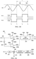
- FIG. 1B shows waveforms of signals generated in the one-sided HHC system 150 shown in FIG. 1A .
- the control signal CTLA 110A transitions from logic low to logic high
- the control signal CTLB 110B transitions from logic high to logic low.
- the VCR 155 intersects with the ramp signal 190 at time t1, triggering the control signal CTLB 110B to transition from logic low to logic high.
- CTLB 110B is logic high and CTLA 110A is logic low from time t1 to time t2, at which CTLB 110B transitions to logic low and CTLA 110A transitions to logic high.
- the length of time between time t0 and t1 while CTLA 110A is logic high is measured, and the time t2 is chosen such that the length of time between t1 and t2 while CTLB 110B is logic low is kept equal to the length of time between t0 and t1.
- the VCR 155 intersects with the ramp 190, and the control signal CTLB 110B transitions from logic low to logic high.
- the time between t1 and t3 is a period T 195.
- one-sided HHC can have slower transient response times than two-sided HHC, shown in FIG. 2A .
- FIG. 2A shows a block diagram of an example analog two-sided HHC system 250 that may be used in place of one-sided HHC system 150 in the LLC converter 100 shown in FIG. 1A .
- the analog two-sided HHC system 250 is described herein with respect to the LLC converter shown in FIG. 1A , and includes an inverter 210, two comparators 260A-B, a pulse-width modulation (PWM) controller 270, an ADC 274, an adder 280, and a ramp generator 285.
- the comparator 260A has a positive input that receives a first ramp 290A from the ramp generator 285 and a negative input that receives the voltage VCR 155 across the resonant capacitor C 115.
- the comparator 260A also receives a feedback signal FDBK 268A from the PWM controller 270 and generates an output signal TRIPA 264A, which is provided to the PWM controller 270.
- the inverter 210 receives the voltage VCR 155 and outputs the inverse, VCR 255 to a negative input of comparator 260B.
- the positive input of comparator 260B receives a second ramp 290B from the ramp generator 285.
- the comparator 260B also receives a feedback signal FDBK 268B from the PWM controller 270 and generates an output signal TRIPB 264B, which is provided to the PWM controller 270.
- the PWM controller 270 generates the feedback signals FDBK 268A and 268B for comparator 260A and 260B, respectively, to reset the DACs in comparators 260A and 260B.
- the PWM controller 270 outputs the control signals CTLA 110A and CTLB 110B for transistors MA and MB, respectively, in the LLC converter 100 shown in FIG. 1A .
- the ADC 274 receives the output voltage Vout 145, and adder 280 subtracts the output of the ADC 274 from a reference signal Vref 278, which represents the target output voltage.
- a voltage controller 283 receives the difference between the target output voltage represented by Vref 278 and the digitized output voltage from ADC 274 and generates a control signal for ramp generator 285.
- the ramp generator 285 receives the control signal from the voltage controller 283 and generates the ramps 290A and 290B for the comparators 260A and 260B, respectively.
- the control signal from the voltage controller 283 indicates the initial values for ramps 290A and 290B.
- FIG. 2B shows waveforms of signals generated in the two-sided HHC system 250 shown in FIG. 2A , including the ramp 290A relative to VCR 155, the ramp 290B relative to VCR 255, and the control signals CTLA 110A and CTLB 110B.
- Ramp 290B is offset from ramp 290A by half a period T 295 of the ramp 290B, and at time t1, VCR 255 intersects with ramp 290B, causing CTLB 110B to transition from logic high to logic low and CTLA 110A to transition from logic low to logic high. At time t2, VCR 155 intersects with ramp 290A, causing CTLA 110A to transition from logic high to logic low and CTLB 110B to transition from logic low to logic high. At t3, VCR 255 intersects with ramp 290B, causing CTLB 110B to transition from logic high to logic low and CTLA 110A to transition from logic low to logic high.
- VCR 155 intersects with ramp 290A, causing CTLA 110A to transition from logic high to logic low and CTLB 110B to transition from logic low to logic high.
- the analog two-sided HHC system 250 offers faster transient response times than one-sided HHC system 150 but utilizes an analog inverter 210 to generate the second feedback signal VCR 255, which can introduce error or delays into the resulting output signal TRIPB 264B from comparator 260B.
- the ramp generator 285 is external to the integrated circuit including the comparators 260A and 260B and PWM controller 270, occupying additional area.
- FIG. 3A shows a block diagram of an example digital two-sided HHC system 350 that may be used in place of one-sided HHC system 150 in the LLC converter 100 shown in FIG. 1A .
- the digital two-sided HHC system 350 is described herein with respect to the LLC converter 100 shown in FIG. 1A , and includes two comparators 360A-B, a PWM controller 370, an ADC 374, an adder 380, a voltage controller 383, and a ramp generator 385.
- the comparator 360A has a positive input that receives a high-side falling ramp RAMP_H 390A from the ramp generator 385 and a negative input that receives the voltage VCR 155 across the resonant capacitor C 115.
- the comparator 360A also receives a feedback signal FDBK 368A from the PWM controller 370 and generates an output signal TRIP_H 364A, which is provided to the PWM controller 370.
- the comparator 360B has a positive input that receives the voltage VCR 155 across the resonant capacitor C 115 and a negative input that receives a low-side rising ramp RAMP_L 390B from the ramp generator 385.
- the comparator 360B also receives a feedback signal FDBK 368B from the PWM controller 370 and generates an output signal TRIP_L 364B, which is provided to the PWM controller 370.
- the PWM controller 370 generates the feedback signals FDBK 368A and 368B for comparator 360A and 360B, respectively.
- the PWM controller 370 outputs the control signals CTLA 110A and CTLB 110B for transistors MA and MB, respectively, in the LLC converter 100 shown in FIG. 1A .
- the ADC 374 receives the output voltage Vout 145, and adder 380 subtracts the output of the ADC 374 from a reference voltage Vref 378, which represents the target output voltage.
- a voltage controller 383 receives the difference between the target output voltage represented by Vref 378 and the digitized output voltage from ADC 374, and generates a control signal for the ramp generator 385.
- the ramp generator 385 receives control signal from the voltage controller 383 and generates the high-side falling ramp RAMP_H 390A and the low-side rising ramp RAMP_L 390B for the comparators 360A and 360B, respectively.
- the control signal from the voltage controller 383 indicates the initial values of the ramp signals RAMP_H 390A and RAMP_L 390B.
- the ramp generator 385 uses preset slopes for each of RAMP_H 390A and RAMP_L 390B, and the feedback signals FDBK 368A and 368B reset the comparator DACs in comparator 360A and 360B to cut off the ramps RAMP_H 390A and RAMP_L 390B.
- FIG. 3B shows waveforms of signals generated in the digital two-sided HHC system 350 shown in FIG. 3A , including the high-side ramp RAMP_H 390A and the low-side ramp RAMP_L 390B relative to VCR 155, and the control signals CTLA 110A and CTLB 110B.
- the low-side ramp RAMP_L 390B is offset from the high-side ramp RAMP_H 390A by half a period T 395 of the ramps 390A and 390B, and at time t1, VCR 155 intersects with low-side ramp RAMP_L 390B, causing CTLB 110B to transition from logic high to logic low and CTLA 110A to transition from logic low to logic high.
- VCR 155 intersects with high-side ramp RAMP_H 390A, causing CTLA 110A to transition from logic high to logic low, and CTLB 110B to transition from logic low to logic high.
- VCR 155 intersects with low-side ramp RAMP_L 390B, causing CTLB 110B to transition from logic high to logic low and CTLA 110A to transition from logic low to logic high.
- VCR 155 intersects with high-side ramp RAMP_H 390A, causing CTLA 110A to transition from logic high to logic low, and CTLB 110B to transition from logic low to logic high.
- the digital two-sided HHC system 350 offers the faster transient response times of a two-sided HHC system relative to one-sided HHC systems and also offers reduced PWM asymmetry compared to the analog two-sided HHC system 250 shown in FIG. 2A by triggering transitions in CTLA 110A and CTLB 110B based on both the high side and the low side of VCR 155.
- the ramp generator 385 is included in the integrated circuit with the comparators 360A-B, PWM controller 370, and the remaining components of digital two-sided HHC system 350.
- FIG. 4A shows a block diagram of an example peak current-mode control (PCMC) DC-DC converter 400 that can be controlled by the digital two-sided HHC system shown in FIG. 3A .
- the PCMC DC-DC converter 400 includes transistors MA and MB, capacitors C 415 and C 430, and inductor L 420.
- the transistors MA and MB are NMOS in this example. In other examples, one or more of MA and MB are PMOS or BJTs.
- the capacitor C 415 has a first terminal coupled to a first terminal of the inductor L 420, and a second terminal.
- the input voltage Vin 405 is applied to the first and second terminals of the capacitor C 415 and the first terminal of the inductor L 420.
- the second terminal of the inductor L 420 is coupled to the drain terminal of MA and the source terminal of MB.
- a current iL 425 flows through the inductor L 420.
- the source terminal of MA is coupled to the second terminal of the capacitor C 415, and the gate terminal of MA is configured to receive the first control signal CTLA 410A.
- the drain terminal of MB is coupled to a first terminal of the capacitor C 430, and the gate terminal of MB is configured to receive the second control signal CTLB 410B.
- the capacitor C 430 has a second terminal coupled to the source terminal of MA and the second terminal of the capacitor C 415.
- the output voltage Vout 445 is taken across the capacitor C 430.
- the digital two-sided HHC system 350 shown in FIG. 3A can be used to provide the control signals CTLA 410A and CTLB 410B.
- FIG. 4B shows waveforms of the current iL 425 through the inductor L 420 shown in the PCMC DC-DC converter 400 shown in FIG. 4A and the high side falling ramp RAMP_H 490A and the low side rising ramp RAMP_L 490B generated in the digital two-sided HHC system used to generate the control signals CTLA 410A and CTLB 410B.
- the current iL 425 intersects with the high side falling ramp RAMP_H 490A, and the control system generates the control signals CTLA 410A and CTLB 410B such that iL 425 decreases.
- iL 425 increases again, and at time t3, iL 425 intersects the high side falling ramp RAMP_H 490A, and the control system generates the control signals CTLA 410A and CTLB 410B such that iL 425 decreases.
- the current iL 425 intersects with the low side rising ramp RAMP_L 490B, and the control system generates the control signals CTLA 410A and CTLB 410B such that the current iL 425 increases.
- FIG. 4C shows a graph of the average current Io 450 over duty cycle D for the PCMC DC-DC converter 400 shown in FIG. 4A .
- Tcharge 455 the capacitors C 415 and 430 are charged, and at the duty cycle Do 465, the average current Io 450 changes directions and the capacitors C 415 and 430 begin to discharge for a time period Tdischarge 460.
- the term "couple” may cover connections, communications, or signal paths that enable a functional relationship consistent with this description. For example, if device A generates a signal to control device B to perform an action: (a) in a first example, device A is coupled to device B by direct connection; or (b) in a second example, device A is coupled to device B through intervening component C if intervening component C does not alter the functional relationship between device A and device B, such that device B is controlled by device A via the control signal generated by device A.
- a device that is "configured to" perform a task or function may be configured (e.g., programmed and/or hardwired) at a time of manufacturing by a manufacturer to perform the function and/or may be configurable (or re-configurable) by a user after manufacturing to perform the function and/or other additional or alternative functions.
- the configuring may be through firmware and/or software programming of the device, through a construction and/or layout of hardware components and interconnections of the device, or a combination thereof.
- terminal As used herein, the terms “terminal”, “node”, “interconnection”, “pin” and “lead” are used interchangeably. Unless specifically stated to the contrary, these terms are generally used to mean an interconnection between or a terminus of a device element, a circuit element, an integrated circuit, a device or other electronics or semiconductor component.
- a circuit or device that is described herein as including certain components may instead be adapted to be coupled to those components to form the described circuitry or device.
- a structure described as including one or more semiconductor elements such as transistors), one or more passive elements (such as resistors, capacitors, and/or inductors), and/or one or more sources (such as voltage and/or current sources) may instead include only the semiconductor elements within a single physical device (e.g., a semiconductor die and/or integrated circuit (IC) package) and may be adapted to be coupled to at least some of the passive elements and/or the sources to form the described structure either at a time of manufacture or after a time of manufacture, for example, by an end-user and/or a third-party.
- semiconductor elements such as transistors
- passive elements such as resistors, capacitors, and/or inductors
- sources such as voltage and/or current sources
- MOSFET metal-oxide-silicon field effect transistor
- BJTs bipolar junction transistors
- Circuits described herein are reconfigurable to include additional or different components to provide functionality at least partially similar to functionality available prior to the component replacement.
- Components shown as resistors are generally representative of any one or more elements coupled in series and/or parallel to provide an amount of impedance represented by the resistor shown.
- a resistor or capacitor shown and described herein as a single component may instead be multiple resistors or capacitors, respectively, coupled in parallel between the same nodes.
- a resistor or capacitor shown and described herein as a single component may instead be multiple resistors or capacitors, respectively, coupled in series between the same two nodes as the single resistor or capacitor.
Landscapes
- Engineering & Computer Science (AREA)
- Power Engineering (AREA)
- Dc-Dc Converters (AREA)
Abstract
Description
- Hybrid hysteretic control (HHC) systems are used to improve the transient response of power supply units by simplifying the compensation into a first order system. Two-sided HHC provides faster transient response times than one-sided HHC, but is implemented with an external comparator and ramp generator, increasing the area occupied by the HHC system on the integrated circuit including the HHC system and the power converter. In addition, unavoidable differences between the two feedback signal chains can introduce imbalance and asymmetry in the resulting pulse width modulation control signals.
- A system comprises a first comparator, a second comparator, a pulse-width modulation (PWM) controller, and a ramp generator. The first comparator has a positive input coupled to a first ramp output of the ramp generator and a negative input configured to receive an input voltage. The second comparator has a positive input configured to receive the input voltage and a negative input coupled to a second ramp output of the ramp generator. The PWM controller is coupled to outputs and control signal inputs of the first and second comparators and has a control output.
- In some implementations, the ramp generator generates a first ramp for the first comparator and a second ramp for the second comparator. The first ramp can be a high-side falling ramp, and the second ramp can be a low-side rising ramp. In some implementations, the ramp generator includes a first ramp generator for the high-side falling ramp and a second ramp for the low-side rising ramp. The first and second ramps are offset by half a period T.
- In some implementations, a voltage sensing circuit provides the input voltage. The input voltage is a first input voltage in some implementations, and the control output of the PWM comprises a first control output and a second control output. The system also includes a first transistor, a second transistor, a third transistor, a fourth transistor, a capacitor, an inductor, and a transformer. The first transistor has a first control terminal coupled to the first control output and first and second current terminals. The second transistor has a second control terminal coupled to the second control output and third and fourth current terminals. The third current terminal is coupled to the second current terminal, and the first and fourth current terminals receive a second input voltage.
- The capacitor has a first capacitor terminal coupled to the fourth current terminal and a second capacitor terminal. The voltage sensing circuit measures the first input voltage across the capacitor. The inductor has a first inductor terminal coupled to the second and third current terminals and a second inductor terminal. The transformer has a first input coupled to the second inductor terminal and a second input coupled to the second capacitor terminal. The transformer also has thee transformer outputs.
- The third transistor has a third control terminal configured to receive a biasing voltage, a fifth current terminal coupled to the first transformer output, and a sixth current terminal. The fourth transistor has a fourth control terminal configured to receive the biasing voltage, a seventh current terminal coupled to the second transformer output, and an eighth current terminal coupled to the sixth current terminal. In some implementations, the transformer is a center-tap transformer.
- For a detailed description of various examples, reference will now be made to the accompanying drawings in which:
-
FIG. 1A shows a block diagram of an example LLC converter and corresponding one-sided hybrid hysteretic control (HHC) system. -
FIG. 1B shows waveforms of signals generated in the one-sided HHC system shown inFIG. 1A . -
FIG. 2A shows a block diagram of an example two-sided HHC system for the LLC converter shown inFIG. 1A . -
FIG. 2B shows waveforms of signals generated in the two-sided HHC system shown inFIG. 2A . -
FIG. 3A shows a block diagram of an example two-sided HHC system for the LLC converter shown inFIG. 1A . -
FIG. 3B shows waveforms of signals generated in the two-sided HHC system shown inFIG. 3A . -
FIG. 4A shows a block diagram of an example peak current-mode control DC-DC converter for the two-sided HHC system shown inFIG. 3A . -
FIG. 4B shows waveforms of signals in the peak current-mode control DC-DC converter shown inFIG. 4A and the two-sided HHC system shown inFIG. 3A . -
FIG. 4C shows a graph of the average current over duty cycle for the peak current-mode control DC-DC converter shown inFIG. 4A . - The same reference number is used in the drawings for the same or similar (either by function and/or structure) features.
- The described digital two-sided hybrid hysteretic control (HHC) systems include two comparators, two ramp generators, and a pulse-width modulation (PWM) controller. Each comparator has a positive input, a negative input, a control input, and an output. In the first comparator, the positive input receives a high-side falling ramp from a ramp generator, and the negative input receives a voltage across a resonant capacitor in a power converter. The control input receives a first feedback signal from the PWM controller. In the second comparator, the positive input receives the voltage across the resonant capacitor, and the negative input receives a low-side rising ramp from the other ramp generator. The control input receives a second feedback signal from the PWM controller, which generates first and second control signals for the power converter based on the outputs of the first and second comparators. The digital two-sided HHC systems are integrated into a single semiconductor die and use both rising and falling ramps, instead of a falling ramp only.
-
FIG. 1A shows a block diagram of anexample LLC converter 100 and corresponding one-sided hybrid hysteretic control (HHC)system 150. TheLLC converter 100 includes transistors MA, MB, MC, and MD;resonant capacitor C 115,inductor L 120,transformer 130,voltage sensing circuit 125, and the one-sided HHC system 150. Thevoltage sensing circuit 125 is configured to measure the voltage across theresonant capacitor C 115. In some implementations, thetransformer 130 is a center-tap transformer. The one-sided HHC system 150 includes acomparator 160, a pulse-width modulation (PWM)controller 170, an analog-to-digital converter (ADC) 174, anadder 180, and aramp generator 185. - The transistors MA, MB, MC, and MD may be metal oxide semiconductor field-effect transistors (MOSFETs). Accordingly, MA-MD are n-type MOSFETs (NMOS) in an example. In other examples, one or more of MA-MD are p-type MOSFETs (PMOS) or bipolar junction transistors (BJTs). A BJT includes a base corresponding to the gate terminal of a MOSFET, and a collector and an emitter corresponding to the drain and source terminals of a MOSFET. The base of a BJT and the gate terminal of a MOSFET are also called control inputs. The collector and emitter of a BJT and the drain and source terminals of a MOSFET are also called current terminals.
- The source terminal of MA and the drain terminal of MB are coupled together, and the
input voltage Vin 105 is applied across the drain terminal of MA and the source terminal of MB. The gate terminal of MA is configured to receive the firstcontrol signal CTLA 110A, and the gate terminal of MB is configured to receive the secondcontrol signal CTLB 110B. Theinductor L 120 has a first terminal coupled to the source terminal of MA and the drain terminal of MB and a second terminal coupled to thetransformer 130. Theresonant capacitor C 115 has a first terminal coupled to the source terminal of MB and a second terminal coupled to thetransformer 130. Thevoltage sensing circuit 125 is coupled to the second terminal of theresonant capacitor C 115 and measures thevoltage VCR 155 across theresonant capacitor C 115. - The
transformer 130 includes a primary winding 134 and a secondary winding 138. The second terminal of theinductor L 120 is coupled to a first terminal of the primary winding 134, and the second terminal of theresonant capacitor C 115 is coupled to a second terminal of the primary winding 134. A first terminal of the secondary winding 138 is coupled to the drain terminal of MD, and a second terminal of the secondary winding 138 is coupled to the drain terminal of MC. The source terminals of MC and MD are coupled together, and the gate terminals of MC and MD are configured to receive a biasingvoltage Vbias 140. Theoutput voltage Vout 145 is taken across the center tap oftransformer 130 and the source terminals of MC and MD. - In the one-
sided HHC system 150, thecomparator 160 has a first input configured to receive thevoltage VCR 155 across theresonant capacitor C 115 from thevoltage sensing circuit 125, and a second input coupled to an output of theramp generator 185 to receive theramp 190. Thecomparator 160 is also configured to receive afeedback signal FDBK 168 from thePWM controller 170, which resets a digital-to-analog converter (DAC) of thecomparator 160 to support HHC. Theoutput 164 ofcomparator 160 is provided to thePWM controller 170, which outputs the control signalsCTLA 110A andCTLB 110B for transistors MA and MB, respectively, as well as thefeedback signal FDBK 168 for thecomparator 160. TheADC 174 receives theoutput voltage Vout 145, andadder 180 subtracts the output of theADC 174 from areference signal Vref 178, which represents the target output voltage. Avoltage controller 183 receives the difference between the target output voltage represented byVref 178 and the digitized output voltage fromADC 174, and generates a control signal for theramp generator 185. Theramp generator 185 receives the control signal from thevoltage controller 183 and generates theramp signal 190. In some implementations, the control signal from thevoltage controller 183 indicates the initial value of theramp signal 190. -
FIG. 1B shows waveforms of signals generated in the one-sided HHC system 150 shown inFIG. 1A . At time t0, thecontrol signal CTLA 110A transitions from logic low to logic high, and thecontrol signal CTLB 110B transitions from logic high to logic low. TheVCR 155 intersects with theramp signal 190 at time t1, triggering thecontrol signal CTLB 110B to transition from logic low to logic high.CTLB 110B is logic high andCTLA 110A is logic low from time t1 to time t2, at whichCTLB 110B transitions to logic low andCTLA 110A transitions to logic high. The length of time between time t0 and t1 whileCTLA 110A is logic high is measured, and the time t2 is chosen such that the length of time between t1 and t2 whileCTLB 110B is logic low is kept equal to the length of time between t0 and t1. At time t3, theVCR 155 intersects with theramp 190, and thecontrol signal CTLB 110B transitions from logic low to logic high. The time between t1 and t3 is aperiod T 195. However, one-sided HHC can have slower transient response times than two-sided HHC, shown inFIG. 2A . -
FIG. 2A shows a block diagram of an example analog two-sided HHC system 250 that may be used in place of one-sided HHC system 150 in theLLC converter 100 shown inFIG. 1A . For ease of explanation, the analog two-sided HHC system 250 is described herein with respect to the LLC converter shown inFIG. 1A , and includes aninverter 210, twocomparators 260A-B, a pulse-width modulation (PWM)controller 270, anADC 274, anadder 280, and aramp generator 285. Thecomparator 260A has a positive input that receives afirst ramp 290A from theramp generator 285 and a negative input that receives thevoltage VCR 155 across theresonant capacitor C 115. Thecomparator 260A also receives afeedback signal FDBK 268A from thePWM controller 270 and generates anoutput signal TRIPA 264A, which is provided to thePWM controller 270. - The
inverter 210 receives thevoltage VCR 155 and outputs the inverse,VCR comparator 260B. The positive input ofcomparator 260B receives asecond ramp 290B from theramp generator 285. Thecomparator 260B also receives afeedback signal FDBK 268B from thePWM controller 270 and generates anoutput signal TRIPB 264B, which is provided to thePWM controller 270. ThePWM controller 270 generates the feedback signalsFDBK comparator comparators PWM controller 270 outputs the control signalsCTLA 110A andCTLB 110B for transistors MA and MB, respectively, in theLLC converter 100 shown inFIG. 1A . - The
ADC 274 receives theoutput voltage Vout 145, andadder 280 subtracts the output of theADC 274 from areference signal Vref 278, which represents the target output voltage. Avoltage controller 283 receives the difference between the target output voltage represented byVref 278 and the digitized output voltage fromADC 274 and generates a control signal forramp generator 285. Theramp generator 285 receives the control signal from thevoltage controller 283 and generates theramps comparators voltage controller 283 indicates the initial values forramps FIG. 2B shows waveforms of signals generated in the two-sided HHC system 250 shown inFIG. 2A , including theramp 290A relative toVCR 155, theramp 290B relative toVCR CTLA 110A andCTLB 110B. -
Ramp 290B is offset fromramp 290A by half aperiod T 295 of theramp 290B, and at time t1,VCR ramp 290B, causingCTLB 110B to transition from logic high to logic low andCTLA 110A to transition from logic low to logic high. At time t2,VCR 155 intersects withramp 290A, causingCTLA 110A to transition from logic high to logic low andCTLB 110B to transition from logic low to logic high. At t3,VCR ramp 290B, causingCTLB 110B to transition from logic high to logic low andCTLA 110A to transition from logic low to logic high. - At time t4,
VCR 155 intersects withramp 290A, causingCTLA 110A to transition from logic high to logic low andCTLB 110B to transition from logic low to logic high. The analog two-sided HHC system 250 offers faster transient response times than one-sided HHC system 150 but utilizes ananalog inverter 210 to generate the secondfeedback signal VCR output signal TRIPB 264B fromcomparator 260B. In addition, theramp generator 285 is external to the integrated circuit including thecomparators PWM controller 270, occupying additional area. -
FIG. 3A shows a block diagram of an example digital two-sided HHC system 350 that may be used in place of one-sided HHC system 150 in theLLC converter 100 shown inFIG. 1A . For ease of explanation, the digital two-sided HHC system 350 is described herein with respect to theLLC converter 100 shown inFIG. 1A , and includes twocomparators 360A-B, aPWM controller 370, anADC 374, anadder 380, avoltage controller 383, and aramp generator 385. Thecomparator 360A has a positive input that receives a high-side fallingramp RAMP_H 390A from theramp generator 385 and a negative input that receives thevoltage VCR 155 across theresonant capacitor C 115. Thecomparator 360A also receives afeedback signal FDBK 368A from thePWM controller 370 and generates anoutput signal TRIP_H 364A, which is provided to thePWM controller 370. - The
comparator 360B has a positive input that receives thevoltage VCR 155 across theresonant capacitor C 115 and a negative input that receives a low-side risingramp RAMP_L 390B from theramp generator 385. Thecomparator 360B also receives afeedback signal FDBK 368B from thePWM controller 370 and generates anoutput signal TRIP_L 364B, which is provided to thePWM controller 370. ThePWM controller 370 generates the feedback signalsFDBK comparator PWM controller 370 outputs the control signalsCTLA 110A andCTLB 110B for transistors MA and MB, respectively, in theLLC converter 100 shown inFIG. 1A . - The
ADC 374 receives theoutput voltage Vout 145, andadder 380 subtracts the output of theADC 374 from areference voltage Vref 378, which represents the target output voltage. Avoltage controller 383 receives the difference between the target output voltage represented byVref 378 and the digitized output voltage fromADC 374, and generates a control signal for theramp generator 385. Theramp generator 385 receives control signal from thevoltage controller 383 and generates the high-side fallingramp RAMP_H 390A and the low-side risingramp RAMP_L 390B for thecomparators voltage controller 383 indicates the initial values of the ramp signalsRAMP_H 390A andRAMP_L 390B. Theramp generator 385 uses preset slopes for each ofRAMP_H 390A andRAMP_L 390B, and the feedback signalsFDBK comparator ramps RAMP_H 390A andRAMP_L 390B. -
FIG. 3B shows waveforms of signals generated in the digital two-sided HHC system 350 shown inFIG. 3A , including the high-side ramp RAMP_H 390A and the low-side ramp RAMP_L 390B relative toVCR 155, and the control signalsCTLA 110A andCTLB 110B. The low-side ramp RAMP_L 390B is offset from the high-side ramp RAMP_H 390A by half aperiod T 395 of theramps VCR 155 intersects with low-side ramp RAMP_L 390B, causingCTLB 110B to transition from logic high to logic low andCTLA 110A to transition from logic low to logic high. At time t2,VCR 155 intersects with high-side ramp RAMP_H 390A, causingCTLA 110A to transition from logic high to logic low, andCTLB 110B to transition from logic low to logic high. At time t3,VCR 155 intersects with low-side ramp RAMP_L 390B, causingCTLB 110B to transition from logic high to logic low andCTLA 110A to transition from logic low to logic high. At time t4,VCR 155 intersects with high-side ramp RAMP_H 390A, causingCTLA 110A to transition from logic high to logic low, andCTLB 110B to transition from logic low to logic high. - The digital two-
sided HHC system 350 offers the faster transient response times of a two-sided HHC system relative to one-sided HHC systems and also offers reduced PWM asymmetry compared to the analog two-sided HHC system 250 shown inFIG. 2A by triggering transitions inCTLA 110A andCTLB 110B based on both the high side and the low side ofVCR 155. In addition, theramp generator 385 is included in the integrated circuit with thecomparators 360A-B,PWM controller 370, and the remaining components of digital two-sided HHC system 350. - The digital two-
sided HHC system 350 shown inFIG. 3A can be used to support advanced topologies such as peak boost converters, peak buck converters, valley boost converters, valley buck converters, and the like. To illustrate,FIG. 4A shows a block diagram of an example peak current-mode control (PCMC) DC-DC converter 400 that can be controlled by the digital two-sided HHC system shown inFIG. 3A . The PCMC DC-DC converter 400 includes transistors MA and MB,capacitors C 415 andC 430, andinductor L 420. The transistors MA and MB are NMOS in this example. In other examples, one or more of MA and MB are PMOS or BJTs. - The
capacitor C 415 has a first terminal coupled to a first terminal of theinductor L 420, and a second terminal. Theinput voltage Vin 405 is applied to the first and second terminals of thecapacitor C 415 and the first terminal of theinductor L 420. The second terminal of theinductor L 420 is coupled to the drain terminal of MA and the source terminal of MB. Acurrent iL 425 flows through theinductor L 420. The source terminal of MA is coupled to the second terminal of thecapacitor C 415, and the gate terminal of MA is configured to receive the firstcontrol signal CTLA 410A. The drain terminal of MB is coupled to a first terminal of thecapacitor C 430, and the gate terminal of MB is configured to receive the secondcontrol signal CTLB 410B. Thecapacitor C 430 has a second terminal coupled to the source terminal of MA and the second terminal of thecapacitor C 415. Theoutput voltage Vout 445 is taken across thecapacitor C 430. - The digital two-
sided HHC system 350 shown inFIG. 3A can be used to provide the control signalsCTLA 410A andCTLB 410B.FIG. 4B shows waveforms of thecurrent iL 425 through theinductor L 420 shown in the PCMC DC-DC converter 400 shown inFIG. 4A and the high side fallingramp RAMP_H 490A and the low side risingramp RAMP_L 490B generated in the digital two-sided HHC system used to generate the control signalsCTLA 410A andCTLB 410B. - At time t1, the
current iL 425 intersects with the high side fallingramp RAMP_H 490A, and the control system generates the control signalsCTLA 410A andCTLB 410B such thatiL 425 decreases. At time t2,iL 425 increases again, and at time t3,iL 425 intersects the high side fallingramp RAMP_H 490A, and the control system generates the control signalsCTLA 410A andCTLB 410B such thatiL 425 decreases. At time t4, thecurrent iL 425 intersects with the low side risingramp RAMP_L 490B, and the control system generates the control signalsCTLA 410A andCTLB 410B such that thecurrent iL 425 increases. At time t5, thecurrent iL 425 decreases again, and at time t6,iL 425 intersects with the low side risingramp RAMP_L 490B, and the control system generates the control signalsCTLA 410A andCTLB 410B such that thecurrent iL 425 increases. -
FIG. 4C shows a graph of the averagecurrent Io 450 over duty cycle D for the PCMC DC-DC converter 400 shown inFIG. 4A . During a firsttime period Tcharge 455, the capacitors C 415 and 430 are charged, and at the duty cycle Do 465, the averagecurrent Io 450 changes directions and the capacitors C 415 and 430 begin to discharge for atime period Tdischarge 460. The duty cycle Do 465 may be represented as:
- In this description, the term "couple" may cover connections, communications, or signal paths that enable a functional relationship consistent with this description. For example, if device A generates a signal to control device B to perform an action: (a) in a first example, device A is coupled to device B by direct connection; or (b) in a second example, device A is coupled to device B through intervening component C if intervening component C does not alter the functional relationship between device A and device B, such that device B is controlled by device A via the control signal generated by device A.
- A device that is "configured to" perform a task or function may be configured (e.g., programmed and/or hardwired) at a time of manufacturing by a manufacturer to perform the function and/or may be configurable (or re-configurable) by a user after manufacturing to perform the function and/or other additional or alternative functions. The configuring may be through firmware and/or software programming of the device, through a construction and/or layout of hardware components and interconnections of the device, or a combination thereof.
- As used herein, the terms "terminal", "node", "interconnection", "pin" and "lead" are used interchangeably. Unless specifically stated to the contrary, these terms are generally used to mean an interconnection between or a terminus of a device element, a circuit element, an integrated circuit, a device or other electronics or semiconductor component.
- A circuit or device that is described herein as including certain components may instead be adapted to be coupled to those components to form the described circuitry or device. For example, a structure described as including one or more semiconductor elements (such as transistors), one or more passive elements (such as resistors, capacitors, and/or inductors), and/or one or more sources (such as voltage and/or current sources) may instead include only the semiconductor elements within a single physical device (e.g., a semiconductor die and/or integrated circuit (IC) package) and may be adapted to be coupled to at least some of the passive elements and/or the sources to form the described structure either at a time of manufacture or after a time of manufacture, for example, by an end-user and/or a third-party.
- While the use of particular transistors is described herein, other transistors (or equivalent devices) may be used instead. For example, a p-type metal-oxide-silicon field effect transistor ("MOSFET") may be used in place of an n-type MOSFET with little or no changes to the circuit. Furthermore, other types of transistors may be used (such as bipolar junction transistors (BJTs)).
- Circuits described herein are reconfigurable to include additional or different components to provide functionality at least partially similar to functionality available prior to the component replacement. Components shown as resistors, unless otherwise stated, are generally representative of any one or more elements coupled in series and/or parallel to provide an amount of impedance represented by the resistor shown. For example, a resistor or capacitor shown and described herein as a single component may instead be multiple resistors or capacitors, respectively, coupled in parallel between the same nodes. For example, a resistor or capacitor shown and described herein as a single component may instead be multiple resistors or capacitors, respectively, coupled in series between the same two nodes as the single resistor or capacitor.
- Unless otherwise stated, "about," "approximately," or "substantially" preceding a value means +/- 10 percent of the stated value. Modifications are possible in the described examples, and other examples are possible within the scope of the claims.
Claims (16)
- A system, comprising:a first comparator having a first positive input, a first negative input, a first control input, and a first output, wherein the first negative input is configured to receive an input voltage;a second comparator having a second positive input, a second negative input, a second control input, and a second output, wherein the second positive input is configured to receive the input voltage;a pulse-width modulation (PWM) controller coupled to the first and second outputs and the first and second control inputs and having a control output; anda ramp generator having a first ramp output coupled to the first positive input and a second ramp output coupled to the second negative input.
- The system of claim 1, wherein the ramp generator is configured to generate a first ramp for the first comparator and a second ramp for the second comparator, wherein the first ramp is a high-side falling ramp, and wherein the second ramp is a low-side rising ramp.
- The system of claim 2, wherein the ramp generator comprises:a first ramp generator having the first ramp output and configured to generate the first ramp for the first comparator; anda second ramp generator having the second ramp output and configured to generate the second ramp for the second comparator.
- The system of claim 2, wherein the first and second ramps are offset by half a period T.
- The system of claim 2, wherein a first control signal generated by the PWM controller and provided to the first control input causes the first ramp to reset, and wherein a second control signal generated by the PWM controller and provided to the second control input causes the second ramp to reset.
- The system of claim 1, further comprising a voltage sensing circuit configured to provide the input voltage.
- The system of claim 6, wherein the input voltage is a first input voltage, wherein the control output comprises a first control output and a second control output, the system further comprising:a first transistor having a first control terminal coupled to the first control output, a first current terminal, and a second current terminal;a second transistor having a second control terminal coupled to the second control output, a third current terminal coupled to the second current terminal, and a fourth current terminal, wherein the first and fourth current terminals are configured to receive a second input voltage;a capacitor having a first capacitor terminal coupled to the fourth current terminal and a second capacitor terminal, wherein the voltage sensing circuit is configured to measure the first input voltage across the capacitor;an inductor having a first inductor terminal coupled to the second and third current terminals and a second inductor terminal;a transformer having a first input coupled to the second inductor terminal, a second input coupled to the second capacitor terminal, a first transformer output, a second transformer output, and a third transformer output;a third transistor having a third control terminal configured to receive a biasing voltage, a fifth current terminal coupled to the first transformer output, and a sixth current terminal; anda fourth transistor having a fourth control terminal configured to receive the biasing voltage, a seventh current terminal coupled to the second transformer output, and an eighth current terminal coupled to the sixth current terminal.
- The system of claim 7, wherein the transformer is a center-tap transformer.
- The system of claim 7, further comprising:an analog-to-digital converter (ADC) configured to receive a voltage across the third transformer output and the sixth and eighth current terminals and having an output;an adder having a positive input configured to receive a reference signal, a negative input coupled to the ADC output, and an output; anda voltage controller having an input coupled to the adder output and an output coupled to the ramp generator; andoptionally, wherein:The ramp generator is configured to generate a first ramp for the first comparator and a second ramp for the second comparator; andthe voltage controller is configured to indicate a first initial frequency for the first ramp and a second initial frequency for the second ramp.
- A device, comprising:a first comparator having a positive input configured to receive a first ramp and a negative input configured to receive an input voltage, wherein the first comparator is configured to generate a first triggering signal;a second comparator having a positive input configured to receive the input voltage and a negative input configured to receive a second ramp, wherein the second comparator is configured to generate a second triggering signal;a pulse-width modulation (PWM) controller configured to:receive the first triggering signal from the first comparator and the second triggering signal from the second comparator;generate a first control signal and a second control signal based on the first and second triggering signals; anda ramp generator configured to generate the first ramp for the first comparator and the second ramp for the second comparator.
- The device of claim 10, wherein the first ramp is a high-side falling ramp and the second ramp is a low-side rising ramp; and
optionally, wherein the first and second ramps are offset by half a period T. - The device of claim 10, wherein:the first comparator further comprises a first control input configured to receive a first feedback signal; andthe second comparator further comprises a second control input configured to receive a second feedback signal; andoptionally, wherein the PWM controller is further configured to generate the first feedback signal for the first comparator and the second feedback signal for the second comparator.
- The device of claim 10, wherein the input voltage is a first input voltage, the device further comprising:a first transistor having a control terminal configured to receive the first control signal, a first current terminal, and a second current terminal;a second transistor having a control terminal configured to receive the second control signal, a third current terminal coupled to the second current terminal, and a fourth current terminal, wherein the first and fourth current terminals are configured to receive a second input voltage;a transformer having a first transformer input, a second transformer input, a first transformer output, a second transformer output, and a third transformer output;a capacitor coupled between the fourth current terminal and the second transformer input;a voltage sensing circuit configured to measure the first input voltage across the capacitor;an inductor coupled between the second and third current terminals and the second transformer input;a third transistor having a control terminal configured to receive a biasing voltage, a fifth current terminal coupled to the first transformer output, and a sixth current terminal; anda fourth transistor having a control terminal configured to receive the biasing voltage, a seventh current terminal coupled to the second transformer output, and an eighth current terminal coupled to the sixth current terminal; andoptionally, wherein the transformer is a center-tap transformer.
- The device of claim 10, further comprising:a first transistor having a control terminal configured to receive the first control signal, a first current terminal, and a second current terminal;a second transistor having a control terminal configured to receive the second control signal, a third current terminal, and a fourth current terminal coupled to the first current terminal;a capacitor having a first capacitor terminal coupled to the second current terminal and a second capacitor terminal;an inductor having a first inductor terminal coupled to the second capacitor terminal and a second inductor terminal coupled to the first and fourth current terminals; anda voltage sensing circuit configured to measure a voltage across the capacitor.
- An apparatus, comprising:a first comparator having a positive input configured to receive a high-side falling ramp and a negative input configured to receive an input voltage, wherein the first comparator is configured to generate a first triggering signal;a second comparator having a positive input configured to receive the input voltage and a negative input configured to receive a low-side rising ramp, wherein the second comparator is configured to generate a second triggering signal, wherein the high-side falling ramp and the low-side rising ramp are offset by half a period T;a pulse-width modulation (PWM) controller configured to:receive the first triggering signal from the first comparator and the second triggering signal from the second comparator;generate a first control signal and a second control signal based on the first and second triggering signals; anda ramp generator configured to generate the high-side falling ramp and the low-side rising ramp.
- The apparatus of claim 15, wherein:the first comparator further comprises a first control input configured to receive a first feedback signal; andthe second comparator further comprises a second control input configured to receive a second feedback signal; andoptionally, wherein the PWM controller is further configured to generate the first feedback signal for the first comparator and the second feedback signal for the second comparator.
Applications Claiming Priority (1)
| Application Number | Priority Date | Filing Date | Title |
|---|---|---|---|
| US17/565,110 US11888482B2 (en) | 2021-12-29 | 2021-12-29 | Hybrid hysteretic control system |
Publications (1)
| Publication Number | Publication Date |
|---|---|
| EP4207568A1 true EP4207568A1 (en) | 2023-07-05 |
Family
ID=84604132
Family Applications (1)
| Application Number | Title | Priority Date | Filing Date |
|---|---|---|---|
| EP22216664.7A Pending EP4207568A1 (en) | 2021-12-29 | 2022-12-23 | A hybrid hysteretic control system |
Country Status (3)
| Country | Link |
|---|---|
| US (1) | US11888482B2 (en) |
| EP (1) | EP4207568A1 (en) |
| CN (1) | CN116365839A (en) |
Cited By (1)
| Publication number | Priority date | Publication date | Assignee | Title |
|---|---|---|---|---|
| WO2025245346A1 (en) * | 2024-05-24 | 2025-11-27 | Texas Instruments Incorporated | Control system for llc voltage converter using up-down counter configured to react to comparator output |
Families Citing this family (1)
| Publication number | Priority date | Publication date | Assignee | Title |
|---|---|---|---|---|
| US20250070656A1 (en) * | 2023-08-22 | 2025-02-27 | Texas Instruments Incorporated | Hysteric control for resonant converters |
Citations (2)
| Publication number | Priority date | Publication date | Assignee | Title |
|---|---|---|---|---|
| US8319570B2 (en) * | 2008-04-18 | 2012-11-27 | Nujira Limited | Pulse width modulation |
| US20180048236A1 (en) * | 2016-08-10 | 2018-02-15 | Texas Instruments Incorporated | Hybrid hysteretic control for llc converters |
Family Cites Families (12)
| Publication number | Priority date | Publication date | Assignee | Title |
|---|---|---|---|---|
| US9397370B2 (en) * | 1999-06-25 | 2016-07-19 | The Board Of Trustees Of The University Of Illinois | Single and multiple cell battery with built-in controller |
| TW201034363A (en) * | 2009-03-13 | 2010-09-16 | Richtek Technology Corp | Buck-boost power converter and its control method |
| US20110227550A1 (en) * | 2010-03-19 | 2011-09-22 | Intersil Americas Inc. | Modulation scheme using a single comparator for constant frequency buck boost converter |
| CN104600983B (en) * | 2014-12-24 | 2017-07-18 | 成都芯源系统有限公司 | Step-up and step-down switch power converter, control circuit and mode switching control unit |
| CN105356743B (en) * | 2015-05-26 | 2018-01-23 | 成都芯源系统有限公司 | Step-up and step-down switching power converter and control circuit thereof |
| DE102015223768B4 (en) * | 2015-11-30 | 2019-10-31 | Dialog Semiconductor (Uk) Limited | Buck-boost converter |
| US10917009B2 (en) * | 2016-08-09 | 2021-02-09 | California Institute Of Technology | Digital multiphase hysteretic point-of-load DC/DC converter |
| US10128757B2 (en) * | 2017-03-03 | 2018-11-13 | Dialog Semiconductor (Uk) Limited | Buck-boost converter with small disturbance at mode transitions |
| TWI681613B (en) * | 2018-02-02 | 2020-01-01 | 茂達電子股份有限公司 | Voltage converter for simulating inductor current control |
| US10404173B1 (en) * | 2018-03-20 | 2019-09-03 | Dialog Semiconductor (Uk) Limited | Buck-boost switching converter |
| US10644600B2 (en) * | 2018-03-25 | 2020-05-05 | Richtek Technology Corporation | Constant-time buck-boost switching regulator and control circuit and control method thereof |
| US11621630B2 (en) * | 2020-08-04 | 2023-04-04 | Texas Instruments Incorporated | Soft-start for switching converter controller with hybrid hysteretic control (HHC) |
-
2021
- 2021-12-29 US US17/565,110 patent/US11888482B2/en active Active
-
2022
- 2022-12-23 EP EP22216664.7A patent/EP4207568A1/en active Pending
- 2022-12-29 CN CN202211705876.7A patent/CN116365839A/en active Pending
Patent Citations (2)
| Publication number | Priority date | Publication date | Assignee | Title |
|---|---|---|---|---|
| US8319570B2 (en) * | 2008-04-18 | 2012-11-27 | Nujira Limited | Pulse width modulation |
| US20180048236A1 (en) * | 2016-08-10 | 2018-02-15 | Texas Instruments Incorporated | Hybrid hysteretic control for llc converters |
Non-Patent Citations (2)
| Title |
|---|
| BASICS COMPARATOR: "MT-083 TUTORIAL Comparators", 30 September 2011 (2011-09-30), pages 1 - 7, XP093043849, Retrieved from the Internet <URL:https://www.analog.com/media/en/training-seminars/tutorials/MT-083.pdf> [retrieved on 20230503] * |
| YANG RICHARD HUA ET AL: "Investigation on the Small Signal Characteristic Based on the LLC Hybrid Hysteretic Charge Control", vol. 4, no. 2, 1 June 2019 (2019-06-01), pages 128 - 142, XP093043409, ISSN: 2475-742X, Retrieved from the Internet <URL:http://tpea.cpss.org.cn/uploads/allimg/190627/10.24295CPSSTPEA.2019.00013.pdf> DOI: 10.24295/CPSSTPEA.2019.00013 * |
Cited By (2)
| Publication number | Priority date | Publication date | Assignee | Title |
|---|---|---|---|---|
| WO2025245346A1 (en) * | 2024-05-24 | 2025-11-27 | Texas Instruments Incorporated | Control system for llc voltage converter using up-down counter configured to react to comparator output |
| US12689281B2 (en) | 2024-05-24 | 2026-07-21 | Texas Instruments Incorporated | Control system for LLC voltage converter using up-down counter configured to react to comparator output |
Also Published As
| Publication number | Publication date |
|---|---|
| US20230208403A1 (en) | 2023-06-29 |
| US11888482B2 (en) | 2024-01-30 |
| CN116365839A (en) | 2023-06-30 |
Similar Documents
| Publication | Publication Date | Title |
|---|---|---|
| CN114337273B (en) | Control circuit with slope compensation and method | |
| US10972009B2 (en) | Multi-phase converter and control circuit thereof | |
| US10554127B2 (en) | Control circuit and control method for multi-output DC-DC converter | |
| US10256727B2 (en) | Multi-phase power supply with DC-DC converter integrated circuits having current sharing function | |
| US8564272B2 (en) | Integrated soft start circuits | |
| TWI483529B (en) | Multi-phase dc-dc power converter | |
| US8203320B2 (en) | Switching mode converters | |
| CN113162368B (en) | DCR current sampling circuit and method and related control circuit | |
| CN111316549B (en) | Self-calibrating DC-DC converter | |
| US12372559B2 (en) | Current sensing for power converter | |
| US11888482B2 (en) | Hybrid hysteretic control system | |
| US20250293602A1 (en) | Peak current limit management for high frequency buck converter | |
| US8541957B2 (en) | Power converter having a feedback circuit for constant loads | |
| US7196499B1 (en) | DC/DC converter with inductor current sensing capability | |
| JP6832082B2 (en) | DC / DC converter and its control circuit, inductor short circuit detection method, control method, electronic equipment | |
| US12206331B2 (en) | DC-DC converter with hybrid current sensing | |
| CN116722738A (en) | Switching power supply converter and control circuit thereof | |
| EP4518128A1 (en) | Control device for a switching voltage regulator and control method | |
| US20260121540A1 (en) | Status report of power stage circuit for multiphase voltage regulator | |
| US20230318442A1 (en) | Battery surge reduction based on early warning signal | |
| Park et al. | Improvements in light-load efficiency and operation frequency for low-voltage current-mode integrated boost converters | |
| US8421436B2 (en) | Step-down converter maintaining stable operation at start up | |
| JP2023013702A (en) | Buck-boost converter, its controller circuit, and electronic equipment using it | |
| US12395061B2 (en) | Controllers configured to detect demagnetization with external bipolar transistors and internal MOS transistors and methods thereof | |
| US20250038644A1 (en) | Switching converter controller with valley current mode control and adjustable peak threshold transitions |
Legal Events
| Date | Code | Title | Description |
|---|---|---|---|
| PUAI | Public reference made under article 153(3) epc to a published international application that has entered the european phase |
Free format text: ORIGINAL CODE: 0009012 |
|
| STAA | Information on the status of an ep patent application or granted ep patent |
Free format text: STATUS: THE APPLICATION HAS BEEN PUBLISHED |
|
| AK | Designated contracting states |
Kind code of ref document: A1 Designated state(s): AL AT BE BG CH CY CZ DE DK EE ES FI FR GB GR HR HU IE IS IT LI LT LU LV MC ME MK MT NL NO PL PT RO RS SE SI SK SM TR |
|
| STAA | Information on the status of an ep patent application or granted ep patent |
Free format text: STATUS: REQUEST FOR EXAMINATION WAS MADE |
|
| 17P | Request for examination filed |
Effective date: 20240105 |
|
| RBV | Designated contracting states (corrected) |
Designated state(s): AL AT BE BG CH CY CZ DE DK EE ES FI FR GB GR HR HU IE IS IT LI LT LU LV MC ME MK MT NL NO PL PT RO RS SE SI SK SM TR |
|
| STAA | Information on the status of an ep patent application or granted ep patent |
Free format text: STATUS: EXAMINATION IS IN PROGRESS |
|
| 17Q | First examination report despatched |
Effective date: 20240917 |