EP4207502A1 - Controlled impedance compressible connector - Google Patents
Controlled impedance compressible connector Download PDFInfo
- Publication number
- EP4207502A1 EP4207502A1 EP22217342.9A EP22217342A EP4207502A1 EP 4207502 A1 EP4207502 A1 EP 4207502A1 EP 22217342 A EP22217342 A EP 22217342A EP 4207502 A1 EP4207502 A1 EP 4207502A1
- Authority
- EP
- European Patent Office
- Prior art keywords
- movable
- terminal
- outer shell
- center terminal
- housing
- Prior art date
- Legal status (The legal status is an assumption and is not a legal conclusion. Google has not performed a legal analysis and makes no representation as to the accuracy of the status listed.)
- Pending
Links
Images



Classifications
-
- H—ELECTRICITY
- H01—ELECTRIC ELEMENTS
- H01R—ELECTRICALLY-CONDUCTIVE CONNECTIONS; STRUCTURAL ASSOCIATIONS OF A PLURALITY OF MUTUALLY-INSULATED ELECTRICAL CONNECTING ELEMENTS; COUPLING DEVICES; CURRENT COLLECTORS
- H01R24/00—Two-part coupling devices, or either of their cooperating parts, characterised by their overall structure
- H01R24/38—Two-part coupling devices, or either of their cooperating parts, characterised by their overall structure having concentrically or coaxially arranged contacts
- H01R24/40—Two-part coupling devices, or either of their cooperating parts, characterised by their overall structure having concentrically or coaxially arranged contacts specially adapted for high frequency
-
- H—ELECTRICITY
- H01—ELECTRIC ELEMENTS
- H01R—ELECTRICALLY-CONDUCTIVE CONNECTIONS; STRUCTURAL ASSOCIATIONS OF A PLURALITY OF MUTUALLY-INSULATED ELECTRICAL CONNECTING ELEMENTS; COUPLING DEVICES; CURRENT COLLECTORS
- H01R24/00—Two-part coupling devices, or either of their cooperating parts, characterised by their overall structure
- H01R24/38—Two-part coupling devices, or either of their cooperating parts, characterised by their overall structure having concentrically or coaxially arranged contacts
- H01R24/40—Two-part coupling devices, or either of their cooperating parts, characterised by their overall structure having concentrically or coaxially arranged contacts specially adapted for high frequency
- H01R24/42—Two-part coupling devices, or either of their cooperating parts, characterised by their overall structure having concentrically or coaxially arranged contacts specially adapted for high frequency comprising impedance matching means or electrical components, e.g. filters or switches
- H01R24/44—Two-part coupling devices, or either of their cooperating parts, characterised by their overall structure having concentrically or coaxially arranged contacts specially adapted for high frequency comprising impedance matching means or electrical components, e.g. filters or switches comprising impedance matching means
-
- H—ELECTRICITY
- H01—ELECTRIC ELEMENTS
- H01R—ELECTRICALLY-CONDUCTIVE CONNECTIONS; STRUCTURAL ASSOCIATIONS OF A PLURALITY OF MUTUALLY-INSULATED ELECTRICAL CONNECTING ELEMENTS; COUPLING DEVICES; CURRENT COLLECTORS
- H01R12/00—Structural associations of a plurality of mutually-insulated electrical connecting elements, specially adapted for printed circuits, e.g. printed circuit boards [PCB], flat or ribbon cables, or like generally planar structures, e.g. terminal strips, terminal blocks; Coupling devices specially adapted for printed circuits, flat or ribbon cables, or like generally planar structures; Terminals specially adapted for contact with, or insertion into, printed circuits, flat or ribbon cables, or like generally planar structures
- H01R12/70—Coupling devices
- H01R12/91—Coupling devices allowing relative movement between coupling parts, e.g. floating or self aligning
-
- H—ELECTRICITY
- H01—ELECTRIC ELEMENTS
- H01R—ELECTRICALLY-CONDUCTIVE CONNECTIONS; STRUCTURAL ASSOCIATIONS OF A PLURALITY OF MUTUALLY-INSULATED ELECTRICAL CONNECTING ELEMENTS; COUPLING DEVICES; CURRENT COLLECTORS
- H01R13/00—Details of coupling devices of the kinds covered by groups H01R12/70 or H01R24/00 - H01R33/00
- H01R13/02—Contact members
-
- H—ELECTRICITY
- H01—ELECTRIC ELEMENTS
- H01R—ELECTRICALLY-CONDUCTIVE CONNECTIONS; STRUCTURAL ASSOCIATIONS OF A PLURALITY OF MUTUALLY-INSULATED ELECTRICAL CONNECTING ELEMENTS; COUPLING DEVICES; CURRENT COLLECTORS
- H01R13/00—Details of coupling devices of the kinds covered by groups H01R12/70 or H01R24/00 - H01R33/00
- H01R13/02—Contact members
- H01R13/22—Contacts for co-operating by abutting
- H01R13/24—Contacts for co-operating by abutting resilient; resiliently-mounted
- H01R13/2407—Contacts for co-operating by abutting resilient; resiliently-mounted characterized by the resilient means
- H01R13/2421—Contacts for co-operating by abutting resilient; resiliently-mounted characterized by the resilient means using coil springs
-
- H—ELECTRICITY
- H01—ELECTRIC ELEMENTS
- H01R—ELECTRICALLY-CONDUCTIVE CONNECTIONS; STRUCTURAL ASSOCIATIONS OF A PLURALITY OF MUTUALLY-INSULATED ELECTRICAL CONNECTING ELEMENTS; COUPLING DEVICES; CURRENT COLLECTORS
- H01R13/00—Details of coupling devices of the kinds covered by groups H01R12/70 or H01R24/00 - H01R33/00
- H01R13/40—Securing contact members in or to a base or case; Insulating of contact members
- H01R13/42—Securing in a demountable manner
-
- H—ELECTRICITY
- H01—ELECTRIC ELEMENTS
- H01R—ELECTRICALLY-CONDUCTIVE CONNECTIONS; STRUCTURAL ASSOCIATIONS OF A PLURALITY OF MUTUALLY-INSULATED ELECTRICAL CONNECTING ELEMENTS; COUPLING DEVICES; CURRENT COLLECTORS
- H01R24/00—Two-part coupling devices, or either of their cooperating parts, characterised by their overall structure
- H01R24/38—Two-part coupling devices, or either of their cooperating parts, characterised by their overall structure having concentrically or coaxially arranged contacts
- H01R24/40—Two-part coupling devices, or either of their cooperating parts, characterised by their overall structure having concentrically or coaxially arranged contacts specially adapted for high frequency
- H01R24/42—Two-part coupling devices, or either of their cooperating parts, characterised by their overall structure having concentrically or coaxially arranged contacts specially adapted for high frequency comprising impedance matching means or electrical components, e.g. filters or switches
-
- H—ELECTRICITY
- H01—ELECTRIC ELEMENTS
- H01R—ELECTRICALLY-CONDUCTIVE CONNECTIONS; STRUCTURAL ASSOCIATIONS OF A PLURALITY OF MUTUALLY-INSULATED ELECTRICAL CONNECTING ELEMENTS; COUPLING DEVICES; CURRENT COLLECTORS
- H01R24/00—Two-part coupling devices, or either of their cooperating parts, characterised by their overall structure
- H01R24/38—Two-part coupling devices, or either of their cooperating parts, characterised by their overall structure having concentrically or coaxially arranged contacts
- H01R24/40—Two-part coupling devices, or either of their cooperating parts, characterised by their overall structure having concentrically or coaxially arranged contacts specially adapted for high frequency
- H01R24/50—Two-part coupling devices, or either of their cooperating parts, characterised by their overall structure having concentrically or coaxially arranged contacts specially adapted for high frequency mounted on a PCB [Printed Circuit Board]
-
- H—ELECTRICITY
- H01—ELECTRIC ELEMENTS
- H01R—ELECTRICALLY-CONDUCTIVE CONNECTIONS; STRUCTURAL ASSOCIATIONS OF A PLURALITY OF MUTUALLY-INSULATED ELECTRICAL CONNECTING ELEMENTS; COUPLING DEVICES; CURRENT COLLECTORS
- H01R24/00—Two-part coupling devices, or either of their cooperating parts, characterised by their overall structure
- H01R24/38—Two-part coupling devices, or either of their cooperating parts, characterised by their overall structure having concentrically or coaxially arranged contacts
- H01R24/40—Two-part coupling devices, or either of their cooperating parts, characterised by their overall structure having concentrically or coaxially arranged contacts specially adapted for high frequency
- H01R24/54—Intermediate parts, e.g. adapters, splitters or elbows
- H01R24/542—Adapters
-
- H—ELECTRICITY
- H01—ELECTRIC ELEMENTS
- H01R—ELECTRICALLY-CONDUCTIVE CONNECTIONS; STRUCTURAL ASSOCIATIONS OF A PLURALITY OF MUTUALLY-INSULATED ELECTRICAL CONNECTING ELEMENTS; COUPLING DEVICES; CURRENT COLLECTORS
- H01R12/00—Structural associations of a plurality of mutually-insulated electrical connecting elements, specially adapted for printed circuits, e.g. printed circuit boards [PCB], flat or ribbon cables, or like generally planar structures, e.g. terminal strips, terminal blocks; Coupling devices specially adapted for printed circuits, flat or ribbon cables, or like generally planar structures; Terminals specially adapted for contact with, or insertion into, printed circuits, flat or ribbon cables, or like generally planar structures
- H01R12/70—Coupling devices
- H01R12/7082—Coupling device supported only by cooperation with PCB
-
- H—ELECTRICITY
- H01—ELECTRIC ELEMENTS
- H01R—ELECTRICALLY-CONDUCTIVE CONNECTIONS; STRUCTURAL ASSOCIATIONS OF A PLURALITY OF MUTUALLY-INSULATED ELECTRICAL CONNECTING ELEMENTS; COUPLING DEVICES; CURRENT COLLECTORS
- H01R12/00—Structural associations of a plurality of mutually-insulated electrical connecting elements, specially adapted for printed circuits, e.g. printed circuit boards [PCB], flat or ribbon cables, or like generally planar structures, e.g. terminal strips, terminal blocks; Coupling devices specially adapted for printed circuits, flat or ribbon cables, or like generally planar structures; Terminals specially adapted for contact with, or insertion into, printed circuits, flat or ribbon cables, or like generally planar structures
- H01R12/70—Coupling devices
- H01R12/71—Coupling devices for rigid printing circuits or like structures
- H01R12/72—Coupling devices for rigid printing circuits or like structures coupling with the edge of the rigid printed circuits or like structures
- H01R12/73—Coupling devices for rigid printing circuits or like structures coupling with the edge of the rigid printed circuits or like structures connecting to other rigid printed circuits or like structures
-
- H—ELECTRICITY
- H01—ELECTRIC ELEMENTS
- H01R—ELECTRICALLY-CONDUCTIVE CONNECTIONS; STRUCTURAL ASSOCIATIONS OF A PLURALITY OF MUTUALLY-INSULATED ELECTRICAL CONNECTING ELEMENTS; COUPLING DEVICES; CURRENT COLLECTORS
- H01R13/00—Details of coupling devices of the kinds covered by groups H01R12/70 or H01R24/00 - H01R33/00
- H01R13/62—Means for facilitating engagement or disengagement of coupling parts or for holding them in engagement
- H01R13/629—Additional means for facilitating engagement or disengagement of coupling parts, e.g. aligning or guiding means, levers, gas pressure electrical locking indicators, manufacturing tolerances
- H01R13/631—Additional means for facilitating engagement or disengagement of coupling parts, e.g. aligning or guiding means, levers, gas pressure electrical locking indicators, manufacturing tolerances for engagement only
- H01R13/6315—Additional means for facilitating engagement or disengagement of coupling parts, e.g. aligning or guiding means, levers, gas pressure electrical locking indicators, manufacturing tolerances for engagement only allowing relative movement between coupling parts, e.g. floating connection
-
- H—ELECTRICITY
- H01—ELECTRIC ELEMENTS
- H01R—ELECTRICALLY-CONDUCTIVE CONNECTIONS; STRUCTURAL ASSOCIATIONS OF A PLURALITY OF MUTUALLY-INSULATED ELECTRICAL CONNECTING ELEMENTS; COUPLING DEVICES; CURRENT COLLECTORS
- H01R2103/00—Two poles
Definitions
- the present invention relates to a compressible coaxial connector or adaptor which has controlled impedance.
- the invention relates to a compressible coaxial connector or adaptor which maintains favorable impedance while accommodating mating engagement variations between mating substrates.
- Coaxial connectors and adaptors for providing interconnection between two mating connector halves or circuit boards is well known in the industry. Impedance within connectors used in high speed applications must be tightly controlled in order to maintain the integrity of the signal, particularly in miniature RF connectors. Impedance is controlled by maintaining accurate spacing between the inner conductor and the outer shell throughout the connector. As spacing between the two mating connector halves or circuit boards may vary due to manufacturing tolerances and the like, such connectors and adaptors need to be able to accommodate variation in mating distances between the two mating connector halves or circuit boards.
- Cable attached contacts such as described in US Patent Number 9,735,519 allow for the contact to absorb the differences in mating distance between the two mating connectors because at least one side is attached to a cable that can move with the spring loaded contact relative to the holding block (or module). For applications where contacts within both mating connectors are connected to substrates, maintaining accurate spacing between the inner and outer conductors (and therefore impedance) across the required mating distance variation becomes difficult.
- a controlled impedance compressible electrical connector having a housing with at least one terminal receiving cavity which extends from a first surface of the housing to a second surface of the housing.
- a terminal assembly is positioned in each of the at least one terminal receiving cavities of the housing.
- the terminal assembly has a first fixed center terminal, a second movable center terminal, a fixed outer shell, a movable outer shell, and a resilient member.
- the terminal assembly is configured to allow impedance of the electrical connector to be maintained as the second movable center terminal and the movable outer shell are moved relative to the first fixed center terminal, the fixed outer shell and the housing.
- An embodiment is directed to a controlled impedance compressible electrical connector having a housing with at least one terminal receiving cavity which extends from a first surface of the housing to a second surface of the housing.
- a terminal assembly is positioned in each of the at least one terminal receiving cavities of the housing.
- the terminal assembly has a first fixed center terminal, a second movable center terminal, a fixed outer shell, a movable outer shell, and a resilient member.
- the terminal assembly is configured to allow impedance of the electrical connector to be maintained as the second movable center terminal and the movable outer shell are moved relative to the first fixed center terminal, the fixed outer shell and the housing.
- An embodiment is directed to a controlled impedance compressible electrical connector for providing an electrical connection between a first mating component and a second mating component.
- the controlled impedance compressible electrical connector has a housing with at least one terminal receiving cavity extending therethrough.
- a terminal assembly is positioned in the at least one terminal receiving cavity.
- the terminal assembly includes a fixed center terminal, a movable outer shell, a movable center terminal and a resilient member.
- the movable outer shell is movable in the at least one terminal receiving cavity and the housing.
- the movable center terminal extends in the movable outer shell.
- the movable center terminal moves in unison with the movable outer shell.
- the relative spacing between the movable center terminal and the movable outer shell is maintained as the movable center terminal and the movable outer shell are moved.
- the resilient member exerts a biasing force on the movable outer shell.
- the movement of the movable outer shell and the movable center terminal relative to the fixed center terminal and the housing allows the controlled impedance compressible electrical connector to accommodate spacing variations between the first mating component and the second mating component.
- the impedance of the electrical connector is maintained as the movable center terminal and the movable outer shell are moved relative to the fixed center terminal and the housing.
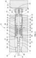
- An illustrative controlled impedance compressible electrical connector or adaptor 10 has a housing 12 with at least one terminal receiving cavity 14 which extends from a first surface 16 of the housing 12 to a second surface 18 of the housing 12.
- the housing 12 is a two piece housing with a main body 20 and a cover 22.
- other configurations of the housing 12, including, but not limited to a one piece housing, may be used.
- a first shoulder 24 extends into the terminal receiving cavity 14 from the housing 12.
- the first shoulder 24 extends inward about the entire circumference of the terminal receiving cavity 14.
- other configurations of the first shoulder 24 may be used.
- the first shoulder 24 is positioned between the first surface 16 and the second surface 18.
- a second shoulder 26 extends into the terminal receiving cavity 14 from the housing 12.
- the second shoulder 26 extends inward about the entire circumference of the terminal receiving cavity 14.
- the second shoulder 26 is positioned between the first surface and the second surface and proximate the first surface 16.
- the second shoulder 26 is provided on the cover 22 of the housing 12.
- a terminal assembly 30 is positioned in each of the at least one terminal receiving cavities 14 of the housing. As shown in FIGS. 1 and 2 , each of the terminal assembly 30 includes a first fixed center terminal 32, a second movable center terminal 34, a fixed outer shell 36, a movable outer shell 38, a resilient member or spring 40 and insulators 42a, 42b and 42c.
- the first fixed center terminal 32 has a first mating section 44 and a second mating section 46.
- the first mating section 44 is a pin and extends from the second surface 18 in a direction away from the first surface 16.
- the first mating section 44 is configured to make an electrical connection to a substrate (not shown).
- the second mating section 46 is a female receptacle for receiving an end of the second movable center terminal 34 therein.
- An insulator 42a is positioned between the first mating section 44 and the second mating section 46.
- the insulator 42a extends about the circumference of the first fixed center terminal 32.
- the insulator 42a is dimensioned to extend from the first fixed center terminal 32 to a wall 48 of the terminal receiving cavity 14.
- the insulator 42a properly positions the first fixed center terminal 32 in the terminal receiving cavity 14 and retains the first fixed center terminal 32 therein.
- the first fixed center terminal 32 is formed from beryllium copper, but other materials having the appropriate conductive and strength characteristics may be used, such as, but not limited to phosphor bronze.
- the insulator 42a may be made from polytetrafluoroethylene (PTFE) or other materials having the appropriate insulative and strength characteristics.
- the second movable center terminal 34 has a first mating section 50 and a second mating section 52.
- the first mating section 50 is a pin.
- the first mating section 50 is configured to make an electrical connection to the second mating section 46 of the first fixed center terminal 32.
- the second mating section 52 of the second movable center terminal 34 is a female receptacle for receiving an end of a mating contact 54 of a second substrate 56.
- the second movable center terminal 34 has sections of different diameters including a first reduced diameter section 58 and a second reduced diameter section 60.
- the second movable center terminal 34 is formed from beryllium copper, but other materials having the appropriate conductive and strength characteristics may be used, such as, but not limited to phosphor bronze.
- a second insulator 42b is positioned in the first reduced diameter section 58.
- the second insulator 42b extends about the circumference of the first reduced diameter section 58.
- the second insulator 42a is dimensioned to extend from the second movable center terminal 34 to the movable outer shell 38.
- the second insulator 42b properly positions the second movable center terminal 34 in the movable outer shell 38 and retains the second movable center terminal 34 therein.
- a third insulator 42c cooperates with the second reduced diameter section 60.
- the third insulator 42c extends about the circumference of the second reduced diameter section 60.
- the third insulator 42c is dimensioned to extend from the second movable center terminal 34 to the movable outer shell 38.
- the third insulator 42c properly positions the second movable center terminal 34 in the movable outer shell 38 and retains the second movable center terminal 34 therein.
- the fixed outer shell 36 has a conductive wall 62 and a back wall 64.
- the conductive wall 62 and a back wall 64 form a first terminal receiving cavity 66.
- the first terminal receiving cavity 66 is dimensioned to receive the first mating section 50 of the second movable center terminal 34 and a portion of the movable outer shell 38 therein.
- the back wall 64 has an opening 68 which is dimensioned to allow the first mating section 50 of the second movable center terminal 34 to extend therethrough and mate with the second mating section 46 of the first fixed center terminal 32.
- a mounting shoulder or projection 70 extends from the conductive wall 62 in a direction away from the first terminal receiving cavity 66. The mounting projection 70 cooperates with the first shoulder 24 of the housing 12 to properly position and secure the fixed outer shell 36 in the terminal receiving cavity 14.
- the movable outer shell 38 includes a first movable outer shell 74 and a second movable outer shell 76.
- first movable outer shell 74 and the second movable outer shell 76 are formed from beryllium copper, but other materials having the appropriate conductive and strength characteristics may be used, such as, but not limited to phosphor bronze.
- the first movable outer shell 74 has a tubular configuration with a conductive outer wall 77.
- the outer wall 77 has a first terminal receiving portion 78 with a first inside diameter of D1, a second terminal receiving portion 80 with a second inside diameter of D2 and a third terminal receiving portion 82 with a third inside diameter D3.
- the third inside diameter D3 is larger than the second inside diameter D2, and the second inside diameter D2 is larger than the first inside diameter of D1.
- the first terminal receiving portion 78 is configured to receive the first reduced diameter section 58 of the second movable center terminal 34.
- the second terminal receiving portion 80 is configured to receive the first reduced diameter section 58 and the second insulator 42b.
- the second terminal receiving portion 80 cooperates with the second insulator 42b to properly position the second movable center terminal 34 in the movable outer shell 38 and retains the second movable center terminal 34 therein.
- the third terminal receiving section 82 is configured to receive a portion of the second movable outer shell 76 and the second movable center terminal 34.
- the second movable outer shell 76 has a tubular configuration with a conductive outer wall 84.
- the outer wall 84 has a first terminal receiving portion 86 with an inside diameter of D4 and a second terminal receiving portion 88 with an inside diameter of D5.
- the inside diameter D4 is slightly larger than the inside diameter D5.
- the inside diameter D5 is approximately equal to the third inside diameter D2 of the first movable outer shell 74, however, other configurations may be used.
- the second terminal receiving portion 88 of the second movable outer shell 76 is configured to receive the second mating section 52 of the second movable center terminal 34.
- the first terminal receiving portion 86 of the second movable outer shell 76 is configured to receive the portion of the second movable center terminal 34 which is proximate the second mating section 52.
- the first terminal receiving portion 86 is also configured to receive the third insulator 42c.
- a shoulder 90 of the first terminal receiving portion 86 cooperates with the third insulator 42c to properly position the second movable center terminal 34 in the movable outer shell 38 and retains the second movable center terminal 34 therein.
- the first terminal receiving portion 86 is also configured to be received in the third terminal receiving section 82 of the first moveable outer shell 74.
- An outer projection or shoulder 92 is provided on the second movable outer shell 76 to facilitate the proper positioning of the second movable outer shell 76 relative to the first movable outer shell 74.
- the spring 40 extends between the fixed outer shell 36 and the movable outer shell 74. In the embodiment shown, the spring 40 extends between the mounting projection 70 of the fixed outer shell 36 and a shoulder 94 of the first movable outer shell 74 of the movable outer shell 38.
- the connector or adaptor 10 Prior to mating with a mating connector or substrate 56, the connector or adaptor 10 is in the position shown in FIG. 3 . In this position, the first mating section 44 of the first fixed center terminal 32 extends beyond the second surface 18 of the housing 12.
- the second terminal receiving portion 88 of the second movable outer shell 76 and the second mating section 52 of the second movable center terminal 34 extend beyond the first surface 18 of the housing 12. While, in this embodiment, the first mating section 44 of the first fixed center terminal 32 extends beyond the second surface 18 of the housing 12, the first mating section 44 other configurations may be used, such as for a surface mount application.
- an end portion of the first mating section 50 of the second movable center terminal 34 is positioned in the second mating section 46 of the first fixed center terminal 32.
- the remainder of the first mating section 50 is positioned in the terminal receiving cavity 66 of the fixed outer shell 36.
- An end portion of the first terminal receiving portion 78 of the first movable outer shell 74 of the movable outer shell 38 is also positioned in the terminal receiving cavity 66 of the fixed outer shell 36.
- the spring 40 In this position, the spring 40 is maintained in a slightly compressed position. Consequently, the spring 40 exerts a force on the mounting projection 70 to bias that fixed outer shell 36 against the first shoulder 24 of the housing 10. In addition, the spring 40 exerts a force on the shoulder 94 of the first movable outer shell 74 of the movable outer shell 38 to bias the projection 92 of the second movable outer shell 76 against the second shoulder 26 of the housing. In so doing, the terminal assembly 30 is maintained in its initial or unmated position by the force of the spring 40. In the initial or unmated position, a space or pocket 67 is provided in the terminal receiving cavity 66 between the first shoulder 24 of the housing 12 and the free end 69 of the conductive outer wall 77 of the first movable outer shell 74.
- the second terminal receiving portion 88 of the second movable outer shell 76 is moved into engagement with an outer shell 55 on the second substrate 56, as shown in FIG. 4 .
- the second mating section 52 of the second movable center terminal 34 is moved into engagement with the mating contact 54 of the second substate 56. In so doing, a coaxial electrical connection is established between the substrate 56 and the adaptor 10.
- the second terminal receiving portion 88 of the second movable outer shell 76 and the second mating section 52 of the second movable center terminal 34 are forced to move inward toward the second surface 18 of the housing 12. As this occurs, the entire terminal assembly 30 is moved from the position shown in FIG. 3 toward the second surface 18 of the housing 12, as shown in FIG. 5 .
- the terminal assembly 30 As the terminal assembly 30 is moved to the position shown in FIG. 5 , the fixed outer shell 36 and the first fixed center terminal 32 remains stationary and does not move. However, the remainder of the terminal assembly 30, including the second movable terminal 38, the first movable outer shell 74 and the second movable outer shell 76 move in unison. Consequently, the positioning and spacing of the second movable center terminal 34 relative to the first movable outer shell 74 and the second movable outer shell 76 does not change as the terminal assembly 30 is moved or slid in the terminal receiving cavity 14. This allows the impedance of the terminal assembly 30 to be properly controlled and maintained as the adaptor 10 is mated to the mating connector or substrates.
- the positioning and spacing of the reduced diameter section 58 of the second movable center terminal 34 is maintained relative to the first terminal receiving portion 78 of the first movable outer shell 74; the positioning and spacing of the reduced diameter section 58 of the second movable center terminal 34 and the second insulator 42b is maintained relative to the second terminal receiving portion 80 of the first movable outer shell 74; the positioning and spacing of the second mating section 52 of the second movable center terminal 34 is maintained relative to the second terminal receiving portion 88 of the second movable outer shell 76; and the positioning and spacing of the portion of the second movable center terminal 34 which is proximate the second mating section 52 and the third insulator 42c is maintained relative to the second terminal receiving portion 88 of the second movable outer shell 76.
- the configuration of, and particularly the spacing of: the reduced diameter section 58 of the second movable center terminal 34 in the first terminal receiving portion 78 of the first movable outer shell 74; the reduced diameter section 58 of the second movable center terminal 34 and the second insulator 42b in the second terminal receiving portion 80 of the first movable outer shell 74; the second mating section 52 of the second movable center terminal 34 in the second terminal receiving portion 88 of the second movable outer shell 76; and the second movable center terminal 34 which is proximate the second mating section 52 and the third insulator 42c in the second terminal receiving portion 88 of the second movable outer shell 76 are calculated such that the impedance in each of these sections matches the impedance in each of the other sections. This allows the signals to be transmitted across each of the sections and across the terminal assembly 30 with little or no loss in signal integrity.
- the first mating section 50 of the second movable center terminal 34 is moved from the first terminal receiving cavity 66 of the fixed outer shell 36 into the second mating section 46 of the first fixed center terminal 32.
- the space or pocket 67 is reduced in size as the free end 69 of the conductive outer wall 77 is moved toward the first shoulder 24 of the housing 12.
- the first terminal receiving cavity 66 of the fixed outer shell 36 and the second mating section 46 of the first fixed center terminal 32 are configured such that the impedance in these section is matched as the movement occurs. This allows the signals to be transmitted across these sections with little or no loss in signal integrity.
- the spring 40 As the terminal assembly 30 is moved from the first position shown in FIG. 3 to the second position shown in FIG. 5 , the spring 40 is further compressed. Consequently, when the adaptor 10 is moved from the second substrate 56, the spring 40 will return toward and unstressed position, thereby exerting a force on the shoulder 94 of the first movable outer shell 74 of the movable outer shell 38, causing the first movable outer shell 74 and the terminal assembly 30 to move back to the initial or unmated position shown in FIG. 3 . In this position, the shoulder 94 of the first movable outer shell 74 of the movable outer shell 38 abuts the second shoulder 26 of the housing 12. Also in this position, the mounting projection 70 cooperates with the first shoulder 24 of the housing 12 to properly position and secure the fixed outer shell 36 in the terminal receiving cavity 14.
- the use of the movable terminal assembly 30 with the biasing spring 40 allows for the adaptor 10 and terminal assembly 30 to provide a controlled and favorable impedance between mating connectors or substrates even when there are mating engagement variations between mating substrates due to manufacturing tolerances and the like.
- the impedance of the terminal assembly 30 is controlled regardless of the distance that the first mating section 50 of the second movable center terminal 34 is moved into the second mating section 46 of the first fixed center terminal 32.
- the impedance is consistently maintained regardless of the position.
- the impedance is controlled in the present invention by maintaining accurate spacing between the inner fixed center conductor or terminal 32, the inner movable center conductor or terminal 34, the fixed outer shell 34 and the movable outer shell 36 throughout the connector.
Landscapes
- Details Of Connecting Devices For Male And Female Coupling (AREA)
- Coupling Device And Connection With Printed Circuit (AREA)
Abstract
Description
- The present invention relates to a compressible coaxial connector or adaptor which has controlled impedance. In particular, the invention relates to a compressible coaxial connector or adaptor which maintains favorable impedance while accommodating mating engagement variations between mating substrates.
- Due to the increasing complexity of electronic components, it is desirable to fit more components in less space on a circuit board or other substrate. Consequently, the spacing between signal traces and contacts within circuit boards has been reduced, while the number of signal traces and contacts housed in the circuit boards has increased, thereby increasing the need for electrical connectors that are capable of handling higher and higher speeds and to do so with greater and greater densities.
- Coaxial connectors and adaptors for providing interconnection between two mating connector halves or circuit boards is well known in the industry. Impedance within connectors used in high speed applications must be tightly controlled in order to maintain the integrity of the signal, particularly in miniature RF connectors. Impedance is controlled by maintaining accurate spacing between the inner conductor and the outer shell throughout the connector. As spacing between the two mating connector halves or circuit boards may vary due to manufacturing tolerances and the like, such connectors and adaptors need to be able to accommodate variation in mating distances between the two mating connector halves or circuit boards. Cable attached contacts such as described in
US Patent Number 9,735,519 - It would, therefore, be beneficial to provide a coaxial connector or adaptor which is compressible and which enables impedance to be maintained across mating distance variations to stabilize signal integrity of board to board connections.
- The solution is provided by a controlled impedance compressible electrical connector having a housing with at least one terminal receiving cavity which extends from a first surface of the housing to a second surface of the housing. A terminal assembly is positioned in each of the at least one terminal receiving cavities of the housing. The terminal assembly has a first fixed center terminal, a second movable center terminal, a fixed outer shell, a movable outer shell, and a resilient member. The terminal assembly is configured to allow impedance of the electrical connector to be maintained as the second movable center terminal and the movable outer shell are moved relative to the first fixed center terminal, the fixed outer shell and the housing.
- The invention will now be described by way of example with reference to the accompanying drawings in which:
-
FIG. 1 is a perspective view of an illustrative embodiment of a contact of an adapter for use in the illustrative coaxial connector system. -
FIG. 2 is an exploded perspective view of the contact ofFIG. 1 . -
FIG. 3 is a cross-sectional view of the contact positioned in a housing of the adaptor, taken along the center axis of the contact, the contact and adaptor are shown prior to mating with an illustrative fixed substrate. -
FIG. 4 is a cross-sectional view of the contact, similar to that ofFIG. 3 , the contact and adaptor are shown partially mated with the illustrative fixed substrate. -
FIG. 5 is a cross-sectional view of the contact, similar to that ofFIG. 3 , the contact and adaptor are shown fully mated with the illustrative fixed substrate. - An embodiment is directed to a controlled impedance compressible electrical connector having a housing with at least one terminal receiving cavity which extends from a first surface of the housing to a second surface of the housing. A terminal assembly is positioned in each of the at least one terminal receiving cavities of the housing. The terminal assembly has a first fixed center terminal, a second movable center terminal, a fixed outer shell, a movable outer shell, and a resilient member. The terminal assembly is configured to allow impedance of the electrical connector to be maintained as the second movable center terminal and the movable outer shell are moved relative to the first fixed center terminal, the fixed outer shell and the housing.
- An embodiment is directed to a controlled impedance compressible electrical connector for providing an electrical connection between a first mating component and a second mating component. The controlled impedance compressible electrical connector has a housing with at least one terminal receiving cavity extending therethrough. A terminal assembly is positioned in the at least one terminal receiving cavity. The terminal assembly includes a fixed center terminal, a movable outer shell, a movable center terminal and a resilient member. The movable outer shell is movable in the at least one terminal receiving cavity and the housing. The movable center terminal extends in the movable outer shell. The movable center terminal moves in unison with the movable outer shell. The relative spacing between the movable center terminal and the movable outer shell is maintained as the movable center terminal and the movable outer shell are moved. The resilient member exerts a biasing force on the movable outer shell. The movement of the movable outer shell and the movable center terminal relative to the fixed center terminal and the housing allows the controlled impedance compressible electrical connector to accommodate spacing variations between the first mating component and the second mating component. The impedance of the electrical connector is maintained as the movable center terminal and the movable outer shell are moved relative to the fixed center terminal and the housing.
- An illustrative controlled impedance compressible electrical connector or
adaptor 10, as shown inFIGS 3 through 5 , has ahousing 12 with at least oneterminal receiving cavity 14 which extends from afirst surface 16 of thehousing 12 to asecond surface 18 of thehousing 12. In the embodiment shown, thehousing 12 is a two piece housing with amain body 20 and acover 22. However, other configurations of thehousing 12, including, but not limited to a one piece housing, may be used. - A
first shoulder 24 extends into theterminal receiving cavity 14 from thehousing 12. In the illustrative embodiment shown, thefirst shoulder 24 extends inward about the entire circumference of theterminal receiving cavity 14. However, other configurations of thefirst shoulder 24 may be used. Thefirst shoulder 24 is positioned between thefirst surface 16 and thesecond surface 18. - A
second shoulder 26 extends into theterminal receiving cavity 14 from thehousing 12. In the illustrative embodiment shown, thesecond shoulder 26 extends inward about the entire circumference of theterminal receiving cavity 14. However, other configurations of thesecond shoulder 26 may be used. Thesecond shoulder 26 is positioned between the first surface and the second surface and proximate thefirst surface 16. In the embodiment shown, thesecond shoulder 26 is provided on thecover 22 of thehousing 12. - A
terminal assembly 30 is positioned in each of the at least oneterminal receiving cavities 14 of the housing. As shown inFIGS. 1 and2 , each of theterminal assembly 30 includes a firstfixed center terminal 32, a secondmovable center terminal 34, a fixedouter shell 36, a movableouter shell 38, a resilient member orspring 40 andinsulators - The first
fixed center terminal 32 has afirst mating section 44 and asecond mating section 46. In the illustrative embodiment shown, thefirst mating section 44 is a pin and extends from thesecond surface 18 in a direction away from thefirst surface 16. Thefirst mating section 44 is configured to make an electrical connection to a substrate (not shown). Thesecond mating section 46 is a female receptacle for receiving an end of the secondmovable center terminal 34 therein. Aninsulator 42a is positioned between thefirst mating section 44 and thesecond mating section 46. Theinsulator 42a extends about the circumference of the firstfixed center terminal 32. Theinsulator 42a is dimensioned to extend from the firstfixed center terminal 32 to awall 48 of theterminal receiving cavity 14. Theinsulator 42a properly positions the firstfixed center terminal 32 in theterminal receiving cavity 14 and retains the firstfixed center terminal 32 therein. In the illustrative embodiment shown, the firstfixed center terminal 32 is formed from beryllium copper, but other materials having the appropriate conductive and strength characteristics may be used, such as, but not limited to phosphor bronze. Theinsulator 42a may be made from polytetrafluoroethylene (PTFE) or other materials having the appropriate insulative and strength characteristics. - The second
movable center terminal 34 has afirst mating section 50 and asecond mating section 52. In the illustrative embodiment shown, thefirst mating section 50 is a pin. Thefirst mating section 50 is configured to make an electrical connection to thesecond mating section 46 of the firstfixed center terminal 32. Thesecond mating section 52 of the secondmovable center terminal 34 is a female receptacle for receiving an end of amating contact 54 of asecond substrate 56. The secondmovable center terminal 34 has sections of different diameters including a first reduceddiameter section 58 and a second reduceddiameter section 60. In the illustrative embodiment shown, the secondmovable center terminal 34 is formed from beryllium copper, but other materials having the appropriate conductive and strength characteristics may be used, such as, but not limited to phosphor bronze. - A
second insulator 42b is positioned in the first reduceddiameter section 58. Thesecond insulator 42b extends about the circumference of the first reduceddiameter section 58. Thesecond insulator 42a is dimensioned to extend from the secondmovable center terminal 34 to the movableouter shell 38. Thesecond insulator 42b properly positions the secondmovable center terminal 34 in the movableouter shell 38 and retains the secondmovable center terminal 34 therein. - A
third insulator 42c cooperates with the second reduceddiameter section 60. Thethird insulator 42c extends about the circumference of the second reduceddiameter section 60. Thethird insulator 42c is dimensioned to extend from the secondmovable center terminal 34 to the movableouter shell 38. Thethird insulator 42c properly positions the secondmovable center terminal 34 in the movableouter shell 38 and retains the secondmovable center terminal 34 therein. - The fixed
outer shell 36 has aconductive wall 62 and aback wall 64. Theconductive wall 62 and aback wall 64 form a firstterminal receiving cavity 66. The firstterminal receiving cavity 66 is dimensioned to receive thefirst mating section 50 of the secondmovable center terminal 34 and a portion of the movableouter shell 38 therein. Theback wall 64 has anopening 68 which is dimensioned to allow thefirst mating section 50 of the secondmovable center terminal 34 to extend therethrough and mate with thesecond mating section 46 of the first fixedcenter terminal 32. A mounting shoulder orprojection 70 extends from theconductive wall 62 in a direction away from the firstterminal receiving cavity 66. The mountingprojection 70 cooperates with thefirst shoulder 24 of thehousing 12 to properly position and secure the fixedouter shell 36 in the terminal receivingcavity 14. - In the illustrative embodiment shown, the movable
outer shell 38 includes a first movableouter shell 74 and a second movableouter shell 76. However, other configurations of the movableouter shell 38 may be used. In the illustrative embodiment shown, the first movableouter shell 74 and the second movableouter shell 76 are formed from beryllium copper, but other materials having the appropriate conductive and strength characteristics may be used, such as, but not limited to phosphor bronze. - The first movable
outer shell 74 has a tubular configuration with a conductiveouter wall 77. Theouter wall 77 has a firstterminal receiving portion 78 with a first inside diameter of D1, a secondterminal receiving portion 80 with a second inside diameter of D2 and a thirdterminal receiving portion 82 with a third inside diameter D3. The third inside diameter D3 is larger than the second inside diameter D2, and the second inside diameter D2 is larger than the first inside diameter of D1. - The first
terminal receiving portion 78 is configured to receive the first reduceddiameter section 58 of the secondmovable center terminal 34. The secondterminal receiving portion 80 is configured to receive the first reduceddiameter section 58 and thesecond insulator 42b. The secondterminal receiving portion 80 cooperates with thesecond insulator 42b to properly position the secondmovable center terminal 34 in the movableouter shell 38 and retains the secondmovable center terminal 34 therein. The thirdterminal receiving section 82 is configured to receive a portion of the second movableouter shell 76 and the secondmovable center terminal 34. - The second movable
outer shell 76 has a tubular configuration with a conductiveouter wall 84. Theouter wall 84 has a firstterminal receiving portion 86 with an inside diameter of D4 and a secondterminal receiving portion 88 with an inside diameter of D5. The inside diameter D4 is slightly larger than the inside diameter D5. In the illustrative embodiment shown, the inside diameter D5 is approximately equal to the third inside diameter D2 of the first movableouter shell 74, however, other configurations may be used. - The second
terminal receiving portion 88 of the second movableouter shell 76 is configured to receive thesecond mating section 52 of the secondmovable center terminal 34. The firstterminal receiving portion 86 of the second movableouter shell 76 is configured to receive the portion of the secondmovable center terminal 34 which is proximate thesecond mating section 52. The firstterminal receiving portion 86 is also configured to receive thethird insulator 42c. Ashoulder 90 of the firstterminal receiving portion 86 cooperates with thethird insulator 42c to properly position the secondmovable center terminal 34 in the movableouter shell 38 and retains the secondmovable center terminal 34 therein. The firstterminal receiving portion 86 is also configured to be received in the thirdterminal receiving section 82 of the first moveableouter shell 74. An outer projection orshoulder 92 is provided on the second movableouter shell 76 to facilitate the proper positioning of the second movableouter shell 76 relative to the first movableouter shell 74. - The
spring 40 extends between the fixedouter shell 36 and the movableouter shell 74. In the embodiment shown, thespring 40 extends between the mountingprojection 70 of the fixedouter shell 36 and ashoulder 94 of the first movableouter shell 74 of the movableouter shell 38. - Prior to mating with a mating connector or
substrate 56, the connector oradaptor 10 is in the position shown inFIG. 3 . In this position, thefirst mating section 44 of the first fixedcenter terminal 32 extends beyond thesecond surface 18 of thehousing 12. The secondterminal receiving portion 88 of the second movableouter shell 76 and thesecond mating section 52 of the secondmovable center terminal 34 extend beyond thefirst surface 18 of thehousing 12. While, in this embodiment, thefirst mating section 44 of the first fixedcenter terminal 32 extends beyond thesecond surface 18 of thehousing 12, thefirst mating section 44 other configurations may be used, such as for a surface mount application. - In the position shown in
FIG. 3 , an end portion of thefirst mating section 50 of the secondmovable center terminal 34 is positioned in thesecond mating section 46 of the first fixedcenter terminal 32. The remainder of thefirst mating section 50 is positioned in the terminal receivingcavity 66 of the fixedouter shell 36. An end portion of the firstterminal receiving portion 78 of the first movableouter shell 74 of the movableouter shell 38 is also positioned in the terminal receivingcavity 66 of the fixedouter shell 36. - In this position, the
spring 40 is maintained in a slightly compressed position. Consequently, thespring 40 exerts a force on the mountingprojection 70 to bias that fixedouter shell 36 against thefirst shoulder 24 of thehousing 10. In addition, thespring 40 exerts a force on theshoulder 94 of the first movableouter shell 74 of the movableouter shell 38 to bias theprojection 92 of the second movableouter shell 76 against thesecond shoulder 26 of the housing. In so doing, theterminal assembly 30 is maintained in its initial or unmated position by the force of thespring 40. In the initial or unmated position, a space orpocket 67 is provided in the terminal receivingcavity 66 between thefirst shoulder 24 of thehousing 12 and thefree end 69 of the conductiveouter wall 77 of the first movableouter shell 74. - As the
adaptor 10 andterminal assembly 30 are moved into engagement with thesecond substrate 56, the secondterminal receiving portion 88 of the second movableouter shell 76 is moved into engagement with anouter shell 55 on thesecond substrate 56, as shown inFIG. 4 . In addition, thesecond mating section 52 of the secondmovable center terminal 34 is moved into engagement with themating contact 54 of thesecond substate 56. In so doing, a coaxial electrical connection is established between thesubstrate 56 and theadaptor 10. - When fully inserted, as shown in
FIG. 5 , the secondterminal receiving portion 88 of the second movableouter shell 76 and thesecond mating section 52 of the secondmovable center terminal 34 are forced to move inward toward thesecond surface 18 of thehousing 12. As this occurs, the entireterminal assembly 30 is moved from the position shown inFIG. 3 toward thesecond surface 18 of thehousing 12, as shown inFIG. 5 . - As the
terminal assembly 30 is moved to the position shown inFIG. 5 , the fixedouter shell 36 and the first fixedcenter terminal 32 remains stationary and does not move. However, the remainder of theterminal assembly 30, including the secondmovable terminal 38, the first movableouter shell 74 and the second movableouter shell 76 move in unison. Consequently, the positioning and spacing of the secondmovable center terminal 34 relative to the first movableouter shell 74 and the second movableouter shell 76 does not change as theterminal assembly 30 is moved or slid in the terminal receivingcavity 14. This allows the impedance of theterminal assembly 30 to be properly controlled and maintained as theadaptor 10 is mated to the mating connector or substrates. - In particular, as the
terminal assembly 30 is moved from the first position shown inFIG. 3 to the second position shown inFIG. 5 : the positioning and spacing of the reduceddiameter section 58 of the secondmovable center terminal 34 is maintained relative to the firstterminal receiving portion 78 of the first movableouter shell 74; the positioning and spacing of the reduceddiameter section 58 of the secondmovable center terminal 34 and thesecond insulator 42b is maintained relative to the secondterminal receiving portion 80 of the first movableouter shell 74; the positioning and spacing of thesecond mating section 52 of the secondmovable center terminal 34 is maintained relative to the secondterminal receiving portion 88 of the second movableouter shell 76; and the positioning and spacing of the portion of the secondmovable center terminal 34 which is proximate thesecond mating section 52 and thethird insulator 42c is maintained relative to the secondterminal receiving portion 88 of the second movableouter shell 76. - The configuration of, and particularly the spacing of: the reduced
diameter section 58 of the secondmovable center terminal 34 in the firstterminal receiving portion 78 of the first movableouter shell 74; the reduceddiameter section 58 of the secondmovable center terminal 34 and thesecond insulator 42b in the secondterminal receiving portion 80 of the first movableouter shell 74; thesecond mating section 52 of the secondmovable center terminal 34 in the secondterminal receiving portion 88 of the second movableouter shell 76; and the secondmovable center terminal 34 which is proximate thesecond mating section 52 and thethird insulator 42c in the secondterminal receiving portion 88 of the second movableouter shell 76 are calculated such that the impedance in each of these sections matches the impedance in each of the other sections. This allows the signals to be transmitted across each of the sections and across theterminal assembly 30 with little or no loss in signal integrity. - During movement of the
terminal assembly 30 from the first position shown inFIG. 3 to the second position shown inFIG. 5 , thefirst mating section 50 of the secondmovable center terminal 34 is moved from the firstterminal receiving cavity 66 of the fixedouter shell 36 into thesecond mating section 46 of the first fixedcenter terminal 32. As this occurs, the space orpocket 67 is reduced in size as thefree end 69 of the conductiveouter wall 77 is moved toward thefirst shoulder 24 of thehousing 12. The firstterminal receiving cavity 66 of the fixedouter shell 36 and thesecond mating section 46 of the first fixedcenter terminal 32 are configured such that the impedance in these section is matched as the movement occurs. This allows the signals to be transmitted across these sections with little or no loss in signal integrity. - As the
terminal assembly 30 is moved from the first position shown inFIG. 3 to the second position shown inFIG. 5 , thespring 40 is further compressed. Consequently, when theadaptor 10 is moved from thesecond substrate 56, thespring 40 will return toward and unstressed position, thereby exerting a force on theshoulder 94 of the first movableouter shell 74 of the movableouter shell 38, causing the first movableouter shell 74 and theterminal assembly 30 to move back to the initial or unmated position shown inFIG. 3 . In this position, theshoulder 94 of the first movableouter shell 74 of the movableouter shell 38 abuts thesecond shoulder 26 of thehousing 12. Also in this position, the mountingprojection 70 cooperates with thefirst shoulder 24 of thehousing 12 to properly position and secure the fixedouter shell 36 in the terminal receivingcavity 14. - In addition, the use of the movable
terminal assembly 30 with the biasingspring 40 allows for theadaptor 10 andterminal assembly 30 to provide a controlled and favorable impedance between mating connectors or substrates even when there are mating engagement variations between mating substrates due to manufacturing tolerances and the like. As theterminal assembly 30 is configured to move as described above, the impedance of theterminal assembly 30 is controlled regardless of the distance that thefirst mating section 50 of the secondmovable center terminal 34 is moved into thesecond mating section 46 of the first fixedcenter terminal 32. As the first movableouter shell 74, the second movableouter shell 76 and the secondmovable center terminal 34 are moved in unison, and as the spacing between the components is maintained regardless of the position in the terminal receivingcavity 14, the impedance is consistently maintained regardless of the position. This allows theadaptor 10 and movableterminal assembly 30 to accommodate variations in mating distance between the two mating connectors or substrates because of manufacturing tolerances in the connectors/substrates and the systems in which they are used. The impedance is controlled in the present invention by maintaining accurate spacing between the inner fixed center conductor or terminal 32, the inner movable center conductor or terminal 34, the fixedouter shell 34 and the movableouter shell 36 throughout the connector.
Claims (15)
- A controlled impedance compressible electrical connector (10) comprising:a housing (12) with at least one terminal receiving cavity (14) extending from a first surface (16) of the housing (12) to a second surface (18) of the housing (12);a terminal assembly (30) positioned in each of the at least one terminal receiving cavities (14) of the housing (12), the terminal assembly (30) having a first fixed center terminal (32), a second movable center terminal (34), a fixed outer shell (36), a movable outer shell (38), and a resilient member (40);wherein the terminal assembly (30) is configured to allow impedance of the electrical connector (10) to be maintained as the second movable center terminal (34) and the movable outer shell (38) are moved relative to the first fixed center terminal (32), the fixed outer shell (36) and the housing (12).
- The controlled impedance compressible electrical connector (10) as recited in claim 1, wherein the housing (12) is a two piece housing (12) with a main body (20) and a cover (22).
- The controlled impedance compressible electrical connector (10) as recited in claim 1 or 2, wherein a first shoulder (24) extends into the terminal receiving cavity (14) from the housing (12), the first shoulder (24) is positioned between the first surface (16) and the second surface (18).
- The controlled impedance compressible electrical connector (10) as recited in claim 3, wherein a second shoulder (26) extends into the terminal receiving cavity (14) from the housing (12), the second shoulder (26) is positioned between the first surface (16) and the second surface (18) and proximate the first surface (16).
- The controlled impedance compressible electrical connector (10) as recited in any preceding claim, wherein the first fixed center terminal (32) has a first mating section (44) and a second mating section (46).
- The controlled impedance compressible electrical connector (10) as recited in claim 5, wherein the first mating section (44) of the first fixed center terminal (32) is a pin which extends from the second surface (18) of the housing (12) in a direction away from the first surface (16) of the housing (12), the second mating section (46) of the first fixed center terminal (32) is a female receptacle for receiving an end of the second movable center terminal (34) therein.
- The controlled impedance compressible electrical connector (10) as recited in claim 5 or 6, wherein a first insulator (42a) is positioned between the first mating section (44) and the second mating section (46), the first insulator (42a) extends about the circumference of the first fixed center terminal (32), the first insulator (42a) positions the first fixed center terminal (32) in the housing (12) and retains the first fixed center terminal (32) therein.
- The controlled impedance compressible electrical connector (10) as recited in any preceding claim, wherein the second movable center terminal (34) has a first mating section (50) and a second mating section (52), the first mating section (50) is configured to make an electrical connection to the first fixed center terminal (32).
- The controlled impedance compressible electrical connector (10) as recited in claim 8, wherein the first mating section (50) is a pin, the second mating section (52) of the second movable center terminal (34) is a female receptacle for receiving an end of a mating contact (54), the second movable center terminal (34) has sections of different diameters including a first reduced diameter section (58) and a second reduced diameter section (60).
- The controlled impedance compressible electrical connector (10) as recited in claim 9, wherein a second insulator (42b) is positioned in the first reduced diameter section (58), the second insulator (42b) extends about the circumference of the first reduced diameter section (58) and is dimensioned to extend from the second movable center terminal (34) to the movable outer shell (38), the second insulator (42b) positions the second movable center terminal (34) in the movable outer shell (38) and retains the second movable center terminal (34) therein.
- The controlled impedance compressible electrical connector (10) as recited in claim 9 or 10, wherein a third insulator (42c) cooperates with the second reduced diameter section (60), the third insulator (42c) extends about the circumference of the second reduced diameter section (60), the third insulator (42c) is dimensioned to extend from the second movable center terminal (34) to the movable outer shell (38), the third insulator (42c) positions the second movable center terminal (34) in the movable outer shell (38) and retains the second movable center terminal (34) therein.
- The controlled impedance compressible electrical connector (10) as recited in any of claims 8 to 11, wherein the fixed outer shell (36) has a conductive wall (62) and a back wall (64), the conductive wall (62) and a back wall (64) form a first terminal receiving cavity (66), the first terminal receiving cavity (66) is dimensioned to receive the first mating section (50) of the second movable center terminal (34) and a portion of the movable outer shell (38) therein, the back wall (64) has an opening (68) which is dimensioned to allow the first mating section (50) of the second movable center terminal (34) to extend therethrough.
- The controlled impedance compressible electrical connector (10) as recited in any preceding claim, wherein the movable outer shell (38) includes a first movable outer shell (74) and a second movable outer shell (76).
- The controlled impedance compressible electrical connector (10) as recited in claim 13, wherein the first movable outer shell (74) has a tubular configuration with a conductive outer wall (77), the outer wall (77) has a first terminal receiving portion (78) with a first inside diameter (D1), a second terminal receiving portion (80) with a second inside diameter (D2) and a third terminal receiving portion (82) with a third inside diameter (D3), the third inside diameter (D3) is larger than the second inside diameter (D2), and the second inside diameter (D2) is larger than the first inside diameter (D1).
- The controlled impedance compressible electrical connector (10) as recited in claim 14, wherein the first terminal receiving portion (78) is configured to receive a first reduced diameter section (58) of the second movable center terminal (34), the second terminal receiving portion (80) is configured to receive the first reduced diameter section (58) and the second insulator (42b), the third terminal receiving portion (82) is configured to receive a portion of the second movable outer shell (76) and the second movable center terminal (34).
Applications Claiming Priority (1)
| Application Number | Priority Date | Filing Date | Title |
|---|---|---|---|
| US17/568,458 US11936145B2 (en) | 2022-01-04 | 2022-01-04 | Controlled impedance compressible connector |
Publications (1)
| Publication Number | Publication Date |
|---|---|
| EP4207502A1 true EP4207502A1 (en) | 2023-07-05 |
Family
ID=84767000
Family Applications (1)
| Application Number | Title | Priority Date | Filing Date |
|---|---|---|---|
| EP22217342.9A Pending EP4207502A1 (en) | 2022-01-04 | 2022-12-30 | Controlled impedance compressible connector |
Country Status (4)
| Country | Link |
|---|---|
| US (1) | US11936145B2 (en) |
| EP (1) | EP4207502A1 (en) |
| CN (1) | CN116404490A (en) |
| CA (1) | CA3185750A1 (en) |
Cited By (1)
| Publication number | Priority date | Publication date | Assignee | Title |
|---|---|---|---|---|
| EP4510390A1 (en) * | 2023-08-14 | 2025-02-19 | Rosenberger Hochfrequenztechnik GmbH & Co. KG | Electrical plug-in connection |
Families Citing this family (2)
| Publication number | Priority date | Publication date | Assignee | Title |
|---|---|---|---|---|
| FR3160825A1 (en) * | 2024-03-28 | 2025-10-03 | Radiall | Unitary RF coaxial connector for board-to-board or board-to-filter or board-to-module connection, with three adjacent coaxial lines of increasing diameter, at least one of which slides into another, with constant impedance matching along the connector axis. |
| US20250323461A1 (en) * | 2024-04-12 | 2025-10-16 | F Time Technology Industrial Co., Ltd. | Coaxial connector |
Citations (4)
| Publication number | Priority date | Publication date | Assignee | Title |
|---|---|---|---|---|
| WO2010075336A1 (en) * | 2008-12-25 | 2010-07-01 | Molex Incorporated | Coaxial connector |
| US9735519B2 (en) | 2015-12-11 | 2017-08-15 | Te Connectivity Corporation | Coaxial connector assembly and communication system having a plurality of coaxial contacts |
| US20210143581A1 (en) * | 2019-11-11 | 2021-05-13 | Commscope Technologies Llc | Coaxial connector and board-to-board connector assembly |
| US20210399468A1 (en) * | 2020-06-23 | 2021-12-23 | TE Connectivity Services Gmbh | Floating coaxial connector with a stabilizing ring at the mating end |
Family Cites Families (4)
| Publication number | Priority date | Publication date | Assignee | Title |
|---|---|---|---|---|
| US9160096B2 (en) * | 2013-12-06 | 2015-10-13 | Tyco Electronics Corporation | High speed connector |
| US10181692B2 (en) * | 2016-11-07 | 2019-01-15 | Corning Optical Communications Rf Llc | Coaxial connector with translating grounding collar for establishing a ground path with a mating connector |
| US10498061B1 (en) * | 2018-12-17 | 2019-12-03 | Te Connectivity Corporation | Coaxial connector assembly |
| US11539167B2 (en) * | 2020-09-17 | 2022-12-27 | Carlisle Interconnect Technologies, Inc. | Adjustable push on connector/adaptor |
-
2022
- 2022-01-04 US US17/568,458 patent/US11936145B2/en active Active
- 2022-12-29 CA CA3185750A patent/CA3185750A1/en active Pending
- 2022-12-30 EP EP22217342.9A patent/EP4207502A1/en active Pending
- 2022-12-30 CN CN202211724272.7A patent/CN116404490A/en active Pending
Patent Citations (4)
| Publication number | Priority date | Publication date | Assignee | Title |
|---|---|---|---|---|
| WO2010075336A1 (en) * | 2008-12-25 | 2010-07-01 | Molex Incorporated | Coaxial connector |
| US9735519B2 (en) | 2015-12-11 | 2017-08-15 | Te Connectivity Corporation | Coaxial connector assembly and communication system having a plurality of coaxial contacts |
| US20210143581A1 (en) * | 2019-11-11 | 2021-05-13 | Commscope Technologies Llc | Coaxial connector and board-to-board connector assembly |
| US20210399468A1 (en) * | 2020-06-23 | 2021-12-23 | TE Connectivity Services Gmbh | Floating coaxial connector with a stabilizing ring at the mating end |
Cited By (1)
| Publication number | Priority date | Publication date | Assignee | Title |
|---|---|---|---|---|
| EP4510390A1 (en) * | 2023-08-14 | 2025-02-19 | Rosenberger Hochfrequenztechnik GmbH & Co. KG | Electrical plug-in connection |
Also Published As
| Publication number | Publication date |
|---|---|
| US11936145B2 (en) | 2024-03-19 |
| CA3185750A1 (en) | 2023-07-04 |
| US20230216255A1 (en) | 2023-07-06 |
| CN116404490A (en) | 2023-07-07 |
Similar Documents
| Publication | Publication Date | Title |
|---|---|---|
| CA3185750A1 (en) | Controlled impedance compressible connector | |
| US7607929B1 (en) | Electrical connector assembly having spring loaded electrical connector | |
| EP1547203B1 (en) | High frequency, blind mate, coaxial interconnect | |
| US6910897B2 (en) | Interconnection system | |
| US7056128B2 (en) | High speed, high density interconnect system for differential and single-ended transmission systems | |
| EP4101034B1 (en) | Protection member to protect resilient arms of a contact assembly from stubbing | |
| EP3930114B1 (en) | Sag limiting coaxial connector | |
| US11539167B2 (en) | Adjustable push on connector/adaptor | |
| CN109782034B (en) | A multi-channel probe | |
| JP2006066384A (en) | Coaxial connector for board-to-board connection | |
| CN111919344B (en) | RF connector including a flat center contact forked at the end to receive contact pins of a complementary connector and a solid insulating structure configured to guide the contact pins | |
| WO1986005035A1 (en) | Coaxial cable terminator | |
| JP2025118994A (en) | Connector Assembly | |
| US11909147B2 (en) | Cable connector assembly | |
| CN113809563A (en) | Bundled cable connection device | |
| EP3926763B1 (en) | Coaxial connector system with adapter | |
| CN105684227A (en) | High-Speed Connectors with Sealed Bases | |
| US8758055B2 (en) | RF module | |
| CN106257753B (en) | Power connector and pluggable connector configured to mate with power connector | |
| US20180375258A1 (en) | Self-aligning cable mating connector | |
| CN223023740U (en) | Telescopic radio frequency connector | |
| CN222422567U (en) | Floating type cable connector | |
| JP2002289311A (en) | Electrical connector | |
| JP2023181712A (en) | coaxial connector |
Legal Events
| Date | Code | Title | Description |
|---|---|---|---|
| PUAI | Public reference made under article 153(3) epc to a published international application that has entered the european phase |
Free format text: ORIGINAL CODE: 0009012 |
|
| STAA | Information on the status of an ep patent application or granted ep patent |
Free format text: STATUS: THE APPLICATION HAS BEEN PUBLISHED |
|
| AK | Designated contracting states |
Kind code of ref document: A1 Designated state(s): AL AT BE BG CH CY CZ DE DK EE ES FI FR GB GR HR HU IE IS IT LI LT LU LV MC ME MK MT NL NO PL PT RO RS SE SI SK SM TR |
|
| STAA | Information on the status of an ep patent application or granted ep patent |
Free format text: STATUS: REQUEST FOR EXAMINATION WAS MADE |
|
| 17P | Request for examination filed |
Effective date: 20240103 |
|
| RBV | Designated contracting states (corrected) |
Designated state(s): AL AT BE BG CH CY CZ DE DK EE ES FI FR GB GR HR HU IE IS IT LI LT LU LV MC ME MK MT NL NO PL PT RO RS SE SI SK SM TR |
|
| STAA | Information on the status of an ep patent application or granted ep patent |
Free format text: STATUS: EXAMINATION IS IN PROGRESS |
|
| 17Q | First examination report despatched |
Effective date: 20250409 |
|
| GRAP | Despatch of communication of intention to grant a patent |
Free format text: ORIGINAL CODE: EPIDOSNIGR1 |
|
| STAA | Information on the status of an ep patent application or granted ep patent |
Free format text: STATUS: GRANT OF PATENT IS INTENDED |
|
| RIC1 | Information provided on ipc code assigned before grant |
Ipc: H01R 12/91 20110101AFI20260526BHEP Ipc: H01R 24/44 20110101ALI20260526BHEP Ipc: H01R 24/50 20110101ALI20260526BHEP Ipc: H01R 12/73 20110101ALN20260526BHEP Ipc: H01R 103/00 20060101ALN20260526BHEP Ipc: H01R 12/70 20110101ALN20260526BHEP |
|
| INTG | Intention to grant announced |
Effective date: 20260611 |