EP4207390A1 - Composite current collector, electrode plate, and electrochemical device - Google Patents
Composite current collector, electrode plate, and electrochemical device Download PDFInfo
- Publication number
- EP4207390A1 EP4207390A1 EP20866942.4A EP20866942A EP4207390A1 EP 4207390 A1 EP4207390 A1 EP 4207390A1 EP 20866942 A EP20866942 A EP 20866942A EP 4207390 A1 EP4207390 A1 EP 4207390A1
- Authority
- EP
- European Patent Office
- Prior art keywords
- layer
- current collector
- film
- composite current
- conductive layer
- Prior art date
- Legal status (The legal status is an assumption and is not a legal conclusion. Google has not performed a legal analysis and makes no representation as to the accuracy of the status listed.)
- Pending
Links
Images
Classifications
-
- H—ELECTRICITY
- H01—ELECTRIC ELEMENTS
- H01M—PROCESSES OR MEANS, e.g. BATTERIES, FOR THE DIRECT CONVERSION OF CHEMICAL ENERGY INTO ELECTRICAL ENERGY
- H01M4/00—Electrodes
- H01M4/02—Electrodes composed of, or comprising, active material
- H01M4/64—Carriers or collectors
- H01M4/66—Selection of materials
- H01M4/665—Composites
-
- H—ELECTRICITY
- H01—ELECTRIC ELEMENTS
- H01M—PROCESSES OR MEANS, e.g. BATTERIES, FOR THE DIRECT CONVERSION OF CHEMICAL ENERGY INTO ELECTRICAL ENERGY
- H01M4/00—Electrodes
- H01M4/02—Electrodes composed of, or comprising, active material
- H01M4/64—Carriers or collectors
- H01M4/66—Selection of materials
- H01M4/665—Composites
- H01M4/667—Composites in the form of layers, e.g. coatings
-
- H—ELECTRICITY
- H01—ELECTRIC ELEMENTS
- H01M—PROCESSES OR MEANS, e.g. BATTERIES, FOR THE DIRECT CONVERSION OF CHEMICAL ENERGY INTO ELECTRICAL ENERGY
- H01M10/00—Secondary cells; Manufacture thereof
- H01M10/05—Accumulators with non-aqueous electrolyte
- H01M10/052—Li-accumulators
-
- H—ELECTRICITY
- H01—ELECTRIC ELEMENTS
- H01M—PROCESSES OR MEANS, e.g. BATTERIES, FOR THE DIRECT CONVERSION OF CHEMICAL ENERGY INTO ELECTRICAL ENERGY
- H01M10/00—Secondary cells; Manufacture thereof
- H01M10/05—Accumulators with non-aqueous electrolyte
- H01M10/052—Li-accumulators
- H01M10/0525—Rocking-chair batteries, i.e. batteries with lithium insertion or intercalation in both electrodes; Lithium-ion batteries
-
- H—ELECTRICITY
- H01—ELECTRIC ELEMENTS
- H01M—PROCESSES OR MEANS, e.g. BATTERIES, FOR THE DIRECT CONVERSION OF CHEMICAL ENERGY INTO ELECTRICAL ENERGY
- H01M4/00—Electrodes
- H01M4/02—Electrodes composed of, or comprising, active material
- H01M4/64—Carriers or collectors
- H01M4/66—Selection of materials
- H01M4/661—Metal or alloys, e.g. alloy coatings
-
- H—ELECTRICITY
- H01—ELECTRIC ELEMENTS
- H01M—PROCESSES OR MEANS, e.g. BATTERIES, FOR THE DIRECT CONVERSION OF CHEMICAL ENERGY INTO ELECTRICAL ENERGY
- H01M4/00—Electrodes
- H01M4/02—Electrodes composed of, or comprising, active material
- H01M4/64—Carriers or collectors
- H01M4/66—Selection of materials
- H01M4/664—Ceramic materials
-
- H—ELECTRICITY
- H01—ELECTRIC ELEMENTS
- H01M—PROCESSES OR MEANS, e.g. BATTERIES, FOR THE DIRECT CONVERSION OF CHEMICAL ENERGY INTO ELECTRICAL ENERGY
- H01M4/00—Electrodes
- H01M4/02—Electrodes composed of, or comprising, active material
- H01M4/64—Carriers or collectors
- H01M4/66—Selection of materials
- H01M4/668—Composites of electroconductive material and synthetic resins
-
- H—ELECTRICITY
- H01—ELECTRIC ELEMENTS
- H01M—PROCESSES OR MEANS, e.g. BATTERIES, FOR THE DIRECT CONVERSION OF CHEMICAL ENERGY INTO ELECTRICAL ENERGY
- H01M4/00—Electrodes
- H01M4/02—Electrodes composed of, or comprising, active material
- H01M4/64—Carriers or collectors
- H01M4/70—Carriers or collectors characterised by shape or form
- H01M4/72—Grids
- H01M4/74—Meshes or woven material; Expanded metal
-
- H—ELECTRICITY
- H01—ELECTRIC ELEMENTS
- H01M—PROCESSES OR MEANS, e.g. BATTERIES, FOR THE DIRECT CONVERSION OF CHEMICAL ENERGY INTO ELECTRICAL ENERGY
- H01M4/00—Electrodes
- H01M4/02—Electrodes composed of, or comprising, active material
- H01M4/64—Carriers or collectors
- H01M4/70—Carriers or collectors characterised by shape or form
- H01M4/80—Porous plates, e.g. sintered carriers
-
- C—CHEMISTRY; METALLURGY
- C23—COATING METALLIC MATERIAL; COATING MATERIAL WITH METALLIC MATERIAL; CHEMICAL SURFACE TREATMENT; DIFFUSION TREATMENT OF METALLIC MATERIAL; COATING BY VACUUM EVAPORATION, BY SPUTTERING, BY ION IMPLANTATION OR BY CHEMICAL VAPOUR DEPOSITION, IN GENERAL; INHIBITING CORROSION OF METALLIC MATERIAL OR INCRUSTATION IN GENERAL
- C23C—COATING METALLIC MATERIAL; COATING MATERIAL WITH METALLIC MATERIAL; SURFACE TREATMENT OF METALLIC MATERIAL BY DIFFUSION INTO THE SURFACE, BY CHEMICAL CONVERSION OR SUBSTITUTION; COATING BY VACUUM EVAPORATION, BY SPUTTERING, BY ION IMPLANTATION OR BY CHEMICAL VAPOUR DEPOSITION, IN GENERAL
- C23C14/00—Coating by vacuum evaporation, by sputtering or by ion implantation of the coating forming material
- C23C14/06—Coating by vacuum evaporation, by sputtering or by ion implantation of the coating forming material characterised by the coating material
- C23C14/08—Oxides
- C23C14/081—Oxides of aluminium, magnesium or beryllium
-
- C—CHEMISTRY; METALLURGY
- C23—COATING METALLIC MATERIAL; COATING MATERIAL WITH METALLIC MATERIAL; CHEMICAL SURFACE TREATMENT; DIFFUSION TREATMENT OF METALLIC MATERIAL; COATING BY VACUUM EVAPORATION, BY SPUTTERING, BY ION IMPLANTATION OR BY CHEMICAL VAPOUR DEPOSITION, IN GENERAL; INHIBITING CORROSION OF METALLIC MATERIAL OR INCRUSTATION IN GENERAL
- C23C—COATING METALLIC MATERIAL; COATING MATERIAL WITH METALLIC MATERIAL; SURFACE TREATMENT OF METALLIC MATERIAL BY DIFFUSION INTO THE SURFACE, BY CHEMICAL CONVERSION OR SUBSTITUTION; COATING BY VACUUM EVAPORATION, BY SPUTTERING, BY ION IMPLANTATION OR BY CHEMICAL VAPOUR DEPOSITION, IN GENERAL
- C23C14/00—Coating by vacuum evaporation, by sputtering or by ion implantation of the coating forming material
- C23C14/06—Coating by vacuum evaporation, by sputtering or by ion implantation of the coating forming material characterised by the coating material
- C23C14/14—Metallic material, boron or silicon
- C23C14/20—Metallic material, boron or silicon on organic substrates
-
- H—ELECTRICITY
- H01—ELECTRIC ELEMENTS
- H01M—PROCESSES OR MEANS, e.g. BATTERIES, FOR THE DIRECT CONVERSION OF CHEMICAL ENERGY INTO ELECTRICAL ENERGY
- H01M4/00—Electrodes
- H01M4/02—Electrodes composed of, or comprising, active material
- H01M4/13—Electrodes for accumulators with non-aqueous electrolyte, e.g. for lithium-accumulators; Processes of manufacture thereof
-
- Y—GENERAL TAGGING OF NEW TECHNOLOGICAL DEVELOPMENTS; GENERAL TAGGING OF CROSS-SECTIONAL TECHNOLOGIES SPANNING OVER SEVERAL SECTIONS OF THE IPC; TECHNICAL SUBJECTS COVERED BY FORMER USPC CROSS-REFERENCE ART COLLECTIONS [XRACs] AND DIGESTS
- Y02—TECHNOLOGIES OR APPLICATIONS FOR MITIGATION OR ADAPTATION AGAINST CLIMATE CHANGE
- Y02E—REDUCTION OF GREENHOUSE GAS [GHG] EMISSIONS, RELATED TO ENERGY GENERATION, TRANSMISSION OR DISTRIBUTION
- Y02E60/00—Enabling technologies; Technologies with a potential or indirect contribution to GHG emissions mitigation
- Y02E60/10—Energy storage using batteries
Definitions
- the application relates to a composite current collector, an electrode plate and an electrochemical device.
- Electrochemical devices can be charged and discharged, and have been widely used in the fields such as consumer products, digital products, power products, medical treatment and security.
- Current collector is the carrier of an active material in an electrochemical device, is an important part of the electrochemical device, and is closely related to the energy density of the electrochemical device.
- a metal polymer film is generally first obtained by metal physical vapor deposition on the surface of a low-density polymer film.
- the current collector In order to make the current collector have better electrical conductivity, it is necessary to deposit a larger thickness of the metal layer on the polymer film, but the increase in the thickness of the current collector will reduce the energy density of the electrochemical device, and the current collector produced in such way is poor in resisting against the corrosion of electrolyte, and the metal layer is likely to fall off during a long-term operation of the electrochemical device and result in failure.
- one aspect of the application is to provide a composite current collector, a passivation layer is formed on one surface of a conductive layer facing toward a connecting layer, the passivation layer may prevent an electrolyte from contacting the conductive layer and causing the conductive layer to be corroded and damaged when the electrolyte enters from one surface of the connecting layer facing away from the conductive layer, thereby improving the stability of the current collector.
- a composite current provided by one embodiment of the application comprises a base body, a first connecting layer and a first conductive layer, the first connecting layer being used for bonding the first conductive layer to a first surface of the base body, and a first passivation layer being formed on one surface of the first conductive layer facing toward the first connecting layer.
- the composite current collector further comprises a second connecting layer and a second conductive layer; the second connecting layer is used for bonding the second conductive layer to a second surface of the base body, and a second passivation layer is formed on one surface of the second conductive layer facing toward the second connecting layer.
- a thickness of the base body is in the range of from 2 ⁇ m to 36 ⁇ m
- a thickness of the first connecting layer is in the range of from 0.2 ⁇ m to 2 ⁇ m
- a thickness of the first conductive layer is in the range of from 100 nm to 5000 nm
- a thickness of the passivation layer is in the range of from 5 nm to 200 nm.
- the base body is at least one selected from the group consisting of a polyethylene film, a polypropylene film, a polyethylene terephthalate film, a polyethylene naphthalate film, a poly(p-phenylene terephthamide) film, a polyimide film, a polycarbonate film, a polyetheretherketone film, a polyoxymethylene film, a poly(p-phenylene sulfide) film, a poly(p-phenylene ether) film, a polyvinyl chloride film, a polyamide film and a polytetrafluoroethylene film.
- the first connecting layer is at least one selected from the group consisting of polyurethane, epoxy resin, polyacrylate, polyvinyl acetate, unsaturated polyester, phenolic resin, urea-formaldehyde resin, modified polyolefin resin, silicone resin, ethylene-acrylic acid copolymer, an ethylene-vinyl acetate copolymer, an ethylene-vinyl alcohol copolymer and polyamide.
- the first passivation layer is at least one selected from the group consisting of an aluminum oxide layer, a titanium oxide layer, a zirconium oxide layer, an aluminum nitride layer, a titanium nitride layer, a titanium carbide layer, a zirconium carbide layer, a silicon dioxide layer, a silicon nitride layer, a silicon carbide layer and an aluminum chromate layer.
- the first conductive layer is at least one selected from the group consisting of aluminum, copper, nickel, iron, titanium, silver, gold, cobalt, chromium, molybdenum and tungsten.
- the first surface of the base body is provided with a groove pattern, and the connecting layer is also filled in the groove pattern.
- the groove pattern is composed of one or more porous structures.
- At least one of the porous structures penetrates through the base body or at least one of the porous structures does not penetrate through the base body.
- the composite current collector comprises a base body, a first connecting layer and a first conductive layer, the first connecting layer being used for bonding the first conductive layer to a first surface of the base body, and a first passivation layer being formed on one surface of the first conductive layer facing toward the first connecting layer.
- the active material layer is formed on one surface of the first conductive layer facing away from the base body of the composite current collector.
- the electrode plate comprises a composite current collector and an active material layer.
- the composite current collector comprises a base body, a first connecting layer and a first conductive layer, the first connecting layer being used for bonding the first conductive layer to a first surface of the base body, and a first passivation layer being formed on one surface of the first conductive layer facing toward first connecting layer,.
- the active material layer is formed on one surface of the first conductive layer facing away from the base body of the composite current collector.
- a passivation layer is formed on one surface of a conductive layer facing toward a connecting layer, the passivation layer may prevent an electrolyte from contacting the conductive layer and causing the conductive layer to be corroded and damaged when the electrolyte enters from one surface of the connecting layer facing away from the conductive layer, and thereby improving the stability of the current collector.
- Base body 10 First surface 11, Second surface 12, First connecting layer 20, First conductive layer 30, First passivation layer 40, Second connecting layer 50, Second conductive layer 60, Second passivation layer 70, Groove pattern 80, Porous structure 81.
- the composite current collector 100 is described according to the embodiments of the application.
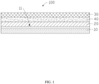
- the current collector 100 comprises a base body 10, a first connecting layer 20, a first conductive layer 30 and a first passivation layer 40.
- the first connecting layer 20 is located between the base body 10 and the first conductive layer 30, and the first passivation layer 40 is formed on one surface of the first conductive layer 30 facing toward the first connecting layer 20.
- One surface of the first connecting layer 20 is bonded to a first surface 11 of the base body 10, and another surface of the first connecting layer 20 is bonded to the first passivation layer 40, so that the first connecting layer 20 is capable of bonding the first conductive layer 30 to a first surface 11 of the base body 10.
- the first passivation layer 40 may be closely attached to the surface of the first conductive layer 30 by means of chemical reaction or vapor deposition.
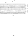
- the composite current collector 100 further comprises a second connecting layer 50, a second conductive layer 60 and a second passivation layer 70.
- the second connecting layer 50 is located between the base body 10 and the second conductive layer 60, and the second passivation layer 70 is formed in one surface of the second conductive layer 60 facing toward the second connecting layer 50.
- One surface of the second connecting layer 50 is bonded to the second surface 11 of the base body 10, and another surface of the second connecting layer 50 is bonded to the second passivation layer 70, so that the second connecting layer 50 is capable of bonding the second conductive layer 60 to a second surface 12 of the base 10.
- the second passivation layer 70 may be closely attached to the surface of the second conductive layer 60 by means of chemical reaction or vapor deposition.
- the first conductive layer 30 and the second conductive layer 60 can be made by a physical vapor deposition process, which can be selected from any one of magnetron sputtering, crucible boat evaporation coating, and electron beam evaporation coating.
- the first conductive layer 30 and the second conductive layer 60 can respectively form a first passivation layer 40 and a second passivation layer 70 on the surfaces thereof by means of processing processes such as electron beam evaporation, DC magnetron sputtering, radio frequency magnetron sputtering, surface oxidation, chemical deposition and spraying.
- the first passivation layer 40 can be used to prevent the electrolyte from contacting the first conductive layer 30 and causing the first conductive layer 30 to be corroded and damaged when the electrolyte enters from one surface of the first connecting layer 20 facing away from the first conductive layer 30.
- the passivation layer 70 can be used to prevent the electrolyte from contacting the second conductive layer 60 and causing the second conductive layer 60 to be corroded and damaged when the electrolyte enters from one surface of the second connection layer 50 facing away from the second conductive layer 60, thereby improving the stability of the composite current collector 100.
- the base body 10 may be at least one selected from the group consisting of a polyethylene film, a polypropylene film, a polyethylene terephthalate film, a polyethylene naphthalate film, a poly(p-phenylene terephthamide) film, a polyimide film, a polycarbonate film, a polyetheretherketone film, a polyoxymethylene film, a poly(p-phenylene sulfide) film, a poly(p-phenylene ether) film, a polyvinyl chloride film, a polyamide film and a polytetrafluoroethylene film.
- the thickness of the base body 10 may be in the range of from 2 ⁇ m to 36 ⁇ m.
- the first connecting layer 20 and the second connecting layer 50 may be at least one respectively selected from the group consisting of polyurethane, epoxy resin, polyacrylate, polyvinyl acetate, unsaturated polyester, phenolic resin, urea-formaldehyde resin, modified polyolefin resin, silicone resin, an ethylene-acrylic acid copolymer, an ethylene-vinyl acetate copolymer, an ethylene-vinyl alcohol copolymer and polyamide.
- the thickness of the first connecting layer 20 and the second connecting layer 50 may both be in the range of from 0.2 ⁇ m to 2 ⁇ m.
- the materials of the first conductive layer 30 and the second conductive layer 60 may be at least one selected from the group consisting of aluminum, copper, nickel, iron, titanium, silver, gold, cobalt, chromium, molybdenum and tungsten.
- the thickness of the first conductive layer 30 and the second conductive layer 60 may both be in the range of from 100 nm to 5000 nm.
- the first passivation layer 40 and the second passivation layer 70 may be at least one respectively selected from the group consisting of an aluminum oxide layer, a titanium oxide layer, a zirconium oxide layer, an aluminum nitride layer, a titanium nitride layer, a titanium carbide layer, a zirconium carbide layer, a silicon dioxide layer, a silicon nitride layer, a silicon carbide layer and an aluminum chromate layer.
- the thickness of the first passivation layer 40 and the second passivation layer 70 may both be in the range of from 5 nm to 200 nm.
- the first passivation layer 40 may also be formed by coating a passivation liquid on one surface of the first conductive layer 30 facing toward the first connection layer 20, and the second passivation layer 70 may also be formed by coating a passivation liquid on one surface of the second conductive layer 60 facing toward the second connecting layer 50.
- the passivation liquid may refer to a solution capable of passivating a metal surface.
- the passivation liquid may form a surface state capable of preventing metal from reacting normally on the metal surface, so as to improve the corrosion resistance thereof.
- a passivation layer is formed on one surface of a conductive layer facing toward a connecting layer, which may prevent an electrolyte from contacting the conductive layer and causing the conductive layer to be corroded and damaged when the electrolyte enters from one surface of the connecting layer facing away from the conductive layer, thereby improving the stability of the current collector.
- the first surface 11 of the base body 10 is provided with a groove pattern 80, and the first connecting layer 20 can also be filled in the groove pattern 80, thereby improving the adhesion between the first connecting layer 20 and the base body 10, so that the first conductive layer 30 is not easy to fall off from the base body 10, thereby further improving the stability of the current collector.
- the first surface 11 of the base body 10 may be subject to patterning treatments such as hole formation and carving to form the groove pattern 80.
- the groove pattern 80 is formed on the first surface 11 by processing methods such as laser drilling, nuclear track etching, chemical etching and photochemical etching.
- the groove pattern 80 may be composed of one or more porous structures 81, and these porous structures may be set to penetrate through the base body 10 or not to penetrate through the base body 10 according to actual needs.
- the plurality of porous structures 81 all penetrate through the base body 10, none of the plurality of porous structures 81 penetrate through the base body 10, or some of the plurality of porous structures 81 penetrate through the base body 10, and the other part of the porous structures do not penetrate through the base body 10.
- the shape of the porous structure 81 may be set according to actual requirements.
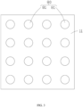
- the porous structure 81 shown in FIG. 3 is a circular pore.
- the porous structure 81 may also be a triangular hole, a quadrilateral hole, a polygonal hole, an irregular shape hole, and the like.
- a second surface 12 of the base body 10 may also be provided with a groove pattern 80, and the second connecting layer 50 is filled in the groove pattern 80, thereby improving the adhesion between the second connecting layer 50 and the base body 10, so that the second conductive layer 60 is not easy to fall off from the base body 10.
- an electrode plate is also disclosed by the application, comprising the composite current collector 100 in any of the cases above.
- one surface of the first conductive layer 30 facing away from the first connecting layer 20 is provided with an active material layer
- one surface of the second conductive layer 60 facing away from the second connecting layer 50 is also provided with the active material layer.
- the active material layer is a cathode active material coating.
- the active material layer is an anode active material coating.
- an electrochemical device comprising an electrode plate in any of the cases above.
- the electrochemical device may be a lithium ion battery, a lithium polymer battery, or the like.
- Contrast Examples 1 to 3 are all composite current collectors without a passivation layer.
- an immersion experiment is performed on the composite current collectors obtained in Embodiments 1 to 6 and Contrast Examples 1 to 3.
- the implementation process may be: cut each composite current collector into current collector splines with a length of 5 cm and a width of 2 cm; immerse the same in an electrolyte and encapsulate with an aluminum plastic film to remove external environmental interference; and finally, place the splines in a constant temperature drying oven at 85°C for 72 hours and then take the same out to observe the appearance of each composite current collector.
- Table 1 The observation results of the composite current collectors in Embodiments 1 to 6 and Contrast Examples 1 to 3 are compiled in Table 1 below.
- the tolerance of the electrolyte of the composite current collector in Embodiments 1-6 is superior to that in Contrast examples 1-3, which indicates that the passivation layer formed on an inner surface of a conductive layer may prevent the electrolyte from contacting the conductive layer and causing the conductive layer to be corroded and damaged when the electrolyte enters from one surface of the connecting layer facing away from the conductive layer, thereby improving the stability of the composite current collector.
Landscapes
- Chemical & Material Sciences (AREA)
- Engineering & Computer Science (AREA)
- Chemical Kinetics & Catalysis (AREA)
- Electrochemistry (AREA)
- General Chemical & Material Sciences (AREA)
- Materials Engineering (AREA)
- Composite Materials (AREA)
- Manufacturing & Machinery (AREA)
- Ceramic Engineering (AREA)
- Cell Electrode Carriers And Collectors (AREA)
- Mechanical Engineering (AREA)
- Metallurgy (AREA)
- Organic Chemistry (AREA)
Abstract
Description
- The application relates to a composite current collector, an electrode plate and an electrochemical device.
- Electrochemical devices can be charged and discharged, and have been widely used in the fields such as consumer products, digital products, power products, medical treatment and security. Current collector is the carrier of an active material in an electrochemical device, is an important part of the electrochemical device, and is closely related to the energy density of the electrochemical device. In the existing process for manufacturing a current collector, a metal polymer film is generally first obtained by metal physical vapor deposition on the surface of a low-density polymer film. In order to make the current collector have better electrical conductivity, it is necessary to deposit a larger thickness of the metal layer on the polymer film, but the increase in the thickness of the current collector will reduce the energy density of the electrochemical device, and the current collector produced in such way is poor in resisting against the corrosion of electrolyte, and the metal layer is likely to fall off during a long-term operation of the electrochemical device and result in failure.
- The application is intended to solve at least one of the technical problems in the prior art. In view of this, one aspect of the application is to provide a composite current collector, a passivation layer is formed on one surface of a conductive layer facing toward a connecting layer, the passivation layer may prevent an electrolyte from contacting the conductive layer and causing the conductive layer to be corroded and damaged when the electrolyte enters from one surface of the connecting layer facing away from the conductive layer, thereby improving the stability of the current collector.
- A composite current provided by one embodiment of the application, comprises a base body, a first connecting layer and a first conductive layer, the first connecting layer being used for bonding the first conductive layer to a first surface of the base body, and a first passivation layer being formed on one surface of the first conductive layer facing toward the first connecting layer.
- In some embodiments, the composite current collector further comprises a second connecting layer and a second conductive layer; the second connecting layer is used for bonding the second conductive layer to a second surface of the base body, and a second passivation layer is formed on one surface of the second conductive layer facing toward the second connecting layer.
- In some embodiments, a thickness of the base body is in the range of from 2 µm to 36 µm, a thickness of the first connecting layer is in the range of from 0.2 µm to 2 µm, a thickness of the first conductive layer is in the range of from 100 nm to 5000 nm, and a thickness of the passivation layer is in the range of from 5 nm to 200 nm.
- In some embodiments, the base body is at least one selected from the group consisting of a polyethylene film, a polypropylene film, a polyethylene terephthalate film, a polyethylene naphthalate film, a poly(p-phenylene terephthamide) film, a polyimide film, a polycarbonate film, a polyetheretherketone film, a polyoxymethylene film, a poly(p-phenylene sulfide) film, a poly(p-phenylene ether) film, a polyvinyl chloride film, a polyamide film and a polytetrafluoroethylene film.
- In some embodiments, the first connecting layer is at least one selected from the group consisting of polyurethane, epoxy resin, polyacrylate, polyvinyl acetate, unsaturated polyester, phenolic resin, urea-formaldehyde resin, modified polyolefin resin, silicone resin, ethylene-acrylic acid copolymer, an ethylene-vinyl acetate copolymer, an ethylene-vinyl alcohol copolymer and polyamide.
- In some embodiments, the first passivation layer is at least one selected from the group consisting of an aluminum oxide layer, a titanium oxide layer, a zirconium oxide layer, an aluminum nitride layer, a titanium nitride layer, a titanium carbide layer, a zirconium carbide layer, a silicon dioxide layer, a silicon nitride layer, a silicon carbide layer and an aluminum chromate layer.
- In some embodiments, the first conductive layer is at least one selected from the group consisting of aluminum, copper, nickel, iron, titanium, silver, gold, cobalt, chromium, molybdenum and tungsten.
- In some embodiments, the first surface of the base body is provided with a groove pattern, and the connecting layer is also filled in the groove pattern.
- In some embodiments, the groove pattern is composed of one or more porous structures.
- In some embodiments, at least one of the porous structures penetrates through the base body or at least one of the porous structures does not penetrate through the base body.
- Another aspect of the application is to provide an electrode plate, comprising a composite current collector and an active material layer. The composite current collector comprises a base body, a first connecting layer and a first conductive layer, the first connecting layer being used for bonding the first conductive layer to a first surface of the base body, and a first passivation layer being formed on one surface of the first conductive layer facing toward the first connecting layer. The active material layer is formed on one surface of the first conductive layer facing away from the base body of the composite current collector.
- Another aspect of the application is to provide an electrochemical device, comprising an electrode plate. The electrode plate comprises a composite current collector and an active material layer. The composite current collector comprises a base body, a first connecting layer and a first conductive layer, the first connecting layer being used for bonding the first conductive layer to a first surface of the base body, and a first passivation layer being formed on one surface of the first conductive layer facing toward first connecting layer,. The active material layer is formed on one surface of the first conductive layer facing away from the base body of the composite current collector.
- In the composite current collector according to the present embodiment of the application, a passivation layer is formed on one surface of a conductive layer facing toward a connecting layer, the passivation layer may prevent an electrolyte from contacting the conductive layer and causing the conductive layer to be corroded and damaged when the electrolyte enters from one surface of the connecting layer facing away from the conductive layer, and thereby improving the stability of the current collector.
- The aspects and advantages mentioned above and/or attached would be clear and easy to understand through the description of embodiments combining the following drawings, wherein:
-
FIG. 1 is a structure diagram of a composite current collector according to one embodiment of the application; -
FIG. 2 is a structure diagram of a composite current collector according to another embodiment of the application; and -
FIG. 3 is a structure diagram of a groove pattern formed in a surface of a base body according to one embodiment of the application. -
Base body 10,First surface 11,Second surface 12, First connectinglayer 20, Firstconductive layer 30,First passivation layer 40, Second connectinglayer 50, Secondconductive layer 60,Second passivation layer 70,Groove pattern 80,Porous structure 81. - The embodiments of the application are described below and examples of said embodiments are shown in the drawings, in which the same or similar reference signs always indicate same or similar elements, or elements with same or similar functions. The exemplary embodiment described by the following figures is to explain the application, but not a limit of the application.
- Referring to
FIG. 1 to FIG. 3 , the compositecurrent collector 100 is described according to the embodiments of the application. - As shown in
FIG. 1 , thecurrent collector 100 according to the embodiments of the application comprises abase body 10, a first connectinglayer 20, a firstconductive layer 30 and afirst passivation layer 40. The first connectinglayer 20 is located between thebase body 10 and the firstconductive layer 30, and thefirst passivation layer 40 is formed on one surface of the firstconductive layer 30 facing toward the first connectinglayer 20. One surface of the first connectinglayer 20 is bonded to afirst surface 11 of thebase body 10, and another surface of the first connectinglayer 20 is bonded to thefirst passivation layer 40, so that the first connectinglayer 20 is capable of bonding the firstconductive layer 30 to afirst surface 11 of thebase body 10. - For example, the
first passivation layer 40 may be closely attached to the surface of the firstconductive layer 30 by means of chemical reaction or vapor deposition. - As shown in
FIG. 2 , the compositecurrent collector 100 further comprises a second connectinglayer 50, a secondconductive layer 60 and asecond passivation layer 70. The second connectinglayer 50 is located between thebase body 10 and the secondconductive layer 60, and thesecond passivation layer 70 is formed in one surface of the secondconductive layer 60 facing toward the second connectinglayer 50. One surface of the second connectinglayer 50 is bonded to thesecond surface 11 of thebase body 10, and another surface of the second connectinglayer 50 is bonded to thesecond passivation layer 70, so that the second connectinglayer 50 is capable of bonding the secondconductive layer 60 to asecond surface 12 of thebase 10. - For example, the
second passivation layer 70 may be closely attached to the surface of the secondconductive layer 60 by means of chemical reaction or vapor deposition. - In some embodiments, the first
conductive layer 30 and the secondconductive layer 60 can be made by a physical vapor deposition process, which can be selected from any one of magnetron sputtering, crucible boat evaporation coating, and electron beam evaporation coating. The firstconductive layer 30 and the secondconductive layer 60 can respectively form afirst passivation layer 40 and asecond passivation layer 70 on the surfaces thereof by means of processing processes such as electron beam evaporation, DC magnetron sputtering, radio frequency magnetron sputtering, surface oxidation, chemical deposition and spraying. Thefirst passivation layer 40 can be used to prevent the electrolyte from contacting the firstconductive layer 30 and causing the firstconductive layer 30 to be corroded and damaged when the electrolyte enters from one surface of the first connectinglayer 20 facing away from the firstconductive layer 30. Thepassivation layer 70 can be used to prevent the electrolyte from contacting the secondconductive layer 60 and causing the secondconductive layer 60 to be corroded and damaged when the electrolyte enters from one surface of thesecond connection layer 50 facing away from the secondconductive layer 60, thereby improving the stability of the compositecurrent collector 100. - In some embodiments, the
base body 10 may be at least one selected from the group consisting of a polyethylene film, a polypropylene film, a polyethylene terephthalate film, a polyethylene naphthalate film, a poly(p-phenylene terephthamide) film, a polyimide film, a polycarbonate film, a polyetheretherketone film, a polyoxymethylene film, a poly(p-phenylene sulfide) film, a poly(p-phenylene ether) film, a polyvinyl chloride film, a polyamide film and a polytetrafluoroethylene film. The thickness of thebase body 10 may be in the range of from 2 µm to 36 µm. - In some embodiments, the first connecting
layer 20 and the second connectinglayer 50 may be at least one respectively selected from the group consisting of polyurethane, epoxy resin, polyacrylate, polyvinyl acetate, unsaturated polyester, phenolic resin, urea-formaldehyde resin, modified polyolefin resin, silicone resin, an ethylene-acrylic acid copolymer, an ethylene-vinyl acetate copolymer, an ethylene-vinyl alcohol copolymer and polyamide. The thickness of the first connectinglayer 20 and the second connectinglayer 50 may both be in the range of from 0.2 µm to 2 µm. - In some embodiments, the materials of the first
conductive layer 30 and the secondconductive layer 60 may be at least one selected from the group consisting of aluminum, copper, nickel, iron, titanium, silver, gold, cobalt, chromium, molybdenum and tungsten. The thickness of the firstconductive layer 30 and the secondconductive layer 60 may both be in the range of from 100 nm to 5000 nm. - In some embodiments, the
first passivation layer 40 and thesecond passivation layer 70 may be at least one respectively selected from the group consisting of an aluminum oxide layer, a titanium oxide layer, a zirconium oxide layer, an aluminum nitride layer, a titanium nitride layer, a titanium carbide layer, a zirconium carbide layer, a silicon dioxide layer, a silicon nitride layer, a silicon carbide layer and an aluminum chromate layer. The thickness of thefirst passivation layer 40 and thesecond passivation layer 70 may both be in the range of from 5 nm to 200 nm. In other embodiments, thefirst passivation layer 40 may also be formed by coating a passivation liquid on one surface of the firstconductive layer 30 facing toward thefirst connection layer 20, and thesecond passivation layer 70 may also be formed by coating a passivation liquid on one surface of the secondconductive layer 60 facing toward the second connectinglayer 50. The passivation liquid may refer to a solution capable of passivating a metal surface. The passivation liquid may form a surface state capable of preventing metal from reacting normally on the metal surface, so as to improve the corrosion resistance thereof. - In the composite
current collector 100 according to the present embodiment of the application, a passivation layer is formed on one surface of a conductive layer facing toward a connecting layer, which may prevent an electrolyte from contacting the conductive layer and causing the conductive layer to be corroded and damaged when the electrolyte enters from one surface of the connecting layer facing away from the conductive layer, thereby improving the stability of the current collector. - As shown in
FIG. 3 , thefirst surface 11 of thebase body 10 is provided with agroove pattern 80, and the first connectinglayer 20 can also be filled in thegroove pattern 80, thereby improving the adhesion between the first connectinglayer 20 and thebase body 10, so that the firstconductive layer 30 is not easy to fall off from thebase body 10, thereby further improving the stability of the current collector. - In some embodiments, the
first surface 11 of thebase body 10 may be subject to patterning treatments such as hole formation and carving to form thegroove pattern 80. For example, thegroove pattern 80 is formed on thefirst surface 11 by processing methods such as laser drilling, nuclear track etching, chemical etching and photochemical etching. - In some embodiments, the
groove pattern 80 may be composed of one or moreporous structures 81, and these porous structures may be set to penetrate through thebase body 10 or not to penetrate through thebase body 10 according to actual needs. For example, the plurality ofporous structures 81 all penetrate through thebase body 10, none of the plurality ofporous structures 81 penetrate through thebase body 10, or some of the plurality ofporous structures 81 penetrate through thebase body 10, and the other part of the porous structures do not penetrate through thebase body 10. - In some embodiments, the shape of the
porous structure 81 may be set according to actual requirements. For example, theporous structure 81 shown inFIG. 3 is a circular pore. Theporous structure 81 may also be a triangular hole, a quadrilateral hole, a polygonal hole, an irregular shape hole, and the like. - In some embodiments, a
second surface 12 of thebase body 10 may also be provided with agroove pattern 80, and the second connectinglayer 50 is filled in thegroove pattern 80, thereby improving the adhesion between the second connectinglayer 50 and thebase body 10, so that the secondconductive layer 60 is not easy to fall off from thebase body 10. - In addition, an electrode plate is also disclosed by the application, comprising the composite
current collector 100 in any of the cases above. - In some embodiments, one surface of the first
conductive layer 30 facing away from the first connectinglayer 20 is provided with an active material layer, and one surface of the secondconductive layer 60 facing away from the second connectinglayer 50 is also provided with the active material layer. Under the condition that the compositecurrent collector 100 is a cathode current collector, the active material layer is a cathode active material coating. Under the condition that the compositecurrent collector 100 is an anode current collector, the active material layer is an anode active material coating. - In addition, an electrochemical device is also disclosed by the application, comprising an electrode plate in any of the cases above. The electrochemical device may be a lithium ion battery, a lithium polymer battery, or the like.
- The following Contrast Examples 1 to 3 are all composite current collectors without a passivation layer.
- Place a polyimide film with a thickness of 50 µm in a vacuum chamber of a crucible boat type vacuum evaporation aluminum plating machine; seal the vacuum chamber and pump the pressure of the vacuum aluminum plating machine to 10-3 Pa; wait until the temperature of a crucible boat is adjusted to 1200to 1500°C; start plating with aluminum; and stop the plating with aluminum after the aluminum degree reaches 200 nm. Carry out corona treatment on a polyethylene terephthalate film with a thickness of 12 µm, and coat the surface thereof with a mixture of bisphenol A epoxy resin and amine curing agent; and in the open time of the coating, carry out hot pressing and compounding on aluminum-plated surfaces of a polyethylene terephthalate film and a polyimide film which are previously treated (the temperature of the hot pressing and compounding is 85°C and the pressure is 0.7 Mpa) to obtain a first contrast composite current collector.
- Place a polyimide film with a thickness of 50 µm in a vacuum chamber of a crucible boat type vacuum evaporation aluminum plating machine; seal the vacuum chamber and pump the pressure of the vacuum aluminum plating machine to 10-3 Pa; wait until the temperature of a crucible boat is adjusted to 1200-1500°C; start plating with aluminum; and stop the plating with aluminum after the aluminum degree reaches 500 nm. Carry out corona treatment on a polyethylene terephthalate film with a thickness of 12 µm , and coat the surface thereof with a mixture of bisphenol A epoxy resin and amine curing agent; and in the open time of the coating, carry out hot pressing and compounding on aluminum-plated surfaces of a polyethylene terephthalate film and a polyimide film which are previously treated (the temperature of the hot pressing and compounding is 85°C and the pressure is 0.7 Mpa) to obtain a second contrast composite current collector.
- Place a polyimide film with a thickness of 50 µm in a vacuum chamber of a crucible boat type vacuum evaporation aluminum plating machine; seal the vacuum chamber and pump the pressure of the vacuum aluminum plating machine to 10-3 Pa; wait until the temperature of a crucible boat is adjusted to 1200-1500°C; start plating with aluminum; and stop the plating with aluminum after the aluminum degree reaches 500 nm. Carry out corona treatment on polyethylene terephthalate film with a thickness of 12 µm, and coat the surface thereof with a single-component polyurethane adhesive; and in the open time of the coating, carry out hot pressing and compounding on aluminum-plated surfaces of a polyethylene terephthalate film and a polyimide film which are previously treated (the temperature of the hot pressing and compounding is 85°C and the pressure is 0.7 Mpa) to obtain a third contrast composite current collector.
- The specific embodiments 1 to 6 described below adopt the composite current collector comprising the passivation layer in the embodiments of the invention.
- Place a polyimide film with a thickness of 50 µm in a vacuum chamber of a crucible boat type vacuum evaporation aluminum plating machine; seal the vacuum chamber and pump the pressure of the vacuum aluminum plating machine to 10-3 Pa; wait until the temperature of a crucible boat is adjusted to 1200-1500°C; start plating with aluminum; stop the plating with aluminum after the aluminum degree reaches 200 nm; and then sputtering an Al2O3 passivation layer with a thickness of 5 nm on the surface of the aluminum layer for use. Carry out corona treatment on a polyethylene terephthalate film with a thickness of 12 µm, and coat the surface thereof with a mixture of bisphenol A epoxy resin and amine curing agent; and in the open time of the coating, carry out hot pressing and compounding on passivated surfaces of aluminum-plated layers of a polyethylene terephthalate film and a polyimide film which are previously treated (the temperature of the hot pressing and compounding is 85°C and the pressure is 0.7 Mpa) to obtain a first composite current collector.
- Place a polyimide film with a thickness of 50 µm in a vacuum chamber of a crucible boat type vacuum evaporation aluminum plating machine; seal the vacuum chamber and pump the pressure of the vacuum aluminum plating machine to 10-3 Pa; wait until the temperature of a crucible boat is adjusted to 1200-1500°C; start plating with aluminum; stop the plating with aluminum after the aluminum degree reaches 500 nm; and then sputtering an Al2O3 passivation layer with a thickness of 10 nm on the surface of the aluminum layer for use. Carry out corona treatment on a polyethylene terephthalate film with a thickness of 12 µm, and coat the surface thereof with a mixture of bisphenol A epoxy resin and amine curing agent; and in the open time of the coating, carry out hot pressing and compounding on passivated surfaces of aluminum-plated layers of a polyethylene terephthalate film and a polyimide film which are previously treated (the temperature of the hot pressing and compounding is 85°C and the pressure is 0.7 Mpa) to obtain a second composite current collector.
- Place a polyimide film with a thickness of 50 µm in a vacuum chamber of a crucible boat type vacuum evaporation aluminum plating machine; seal the vacuum chamber and pump the pressure of the vacuum aluminum plating machine to 10-3 Pa; wait until the temperature of a crucible boat is adjusted to 1200-1500°C; start plating with aluminum; stop the plating with aluminum after the aluminum degree reaches 500 nm; and then sputtering an Al2O3 passivation layer with a thickness of 20 nm on the surface of the aluminum layer for use. Carry out corona treatment on a polyethylene terephthalate film with a thickness of 12 µm, and coat the surface thereof with a mixture of bisphenol A epoxy resin and amine curing agent; and in the open time of the coating, carry out hot pressing and compounding on passivated surfaces of aluminum-plated layers of a polyethylene terephthalate film and a polyimide film which are previously treated (the temperature of the hot pressing and compounding is 85°C and the pressure is 0.7 Mpa) to obtain a third composite current collector.
- Place a polyimide film with a thickness of 50 µm in a vacuum chamber of a crucible boat type vacuum evaporation aluminum plating machine; seal the vacuum chamber and pump the pressure of the vacuum aluminum plating machine to 10-3 Pa; wait until the temperature of a crucible boat is adjusted to 1200-1500°C; start plating with aluminum; stop the plating with aluminum after the aluminum degree reaches 500 nm; and then sputtering an Al2O3 passivation layer with a thickness of 20 nm on the surface of the aluminum layer for use. Carry out corona treatment on a polyethylene terephthalate film with a thickness of 12 µm, and coat the surface thereof with a single-component polyurethane adhesive; and in the open time of the coating, carry out hot pressing and compounding on passivated surfaces of aluminum-plated layers of a polyethylene terephthalate film and a polyimide film which are previously treated (the temperature of the hot pressing and compounding is 85°C and the pressure is 0.7 Mpa) to obtain a fourth contrast composite current collector.
- Place a polyimide film with a thickness of 50 µm in a vacuum chamber of a crucible boat type vacuum evaporation aluminum plating machine; seal the vacuum chamber and pump the pressure of the vacuum aluminum plating machine to 10-3 Pa; wait until the temperature of a crucible boat is adjusted to 1200-1500°C; start plating with aluminum; stop the plating with aluminum after the aluminum degree reaches 500 nm; and then sputtering a TiO2 passivation layer with a thickness of 20 nm on the surface of the aluminum layer for use. Carry out corona treatment on a polyethylene terephthalate film with a thickness of 12 µm, and coat the surface thereof with a single-component polyurethane adhesive; and in the open time of the coating, carry out hot pressing and compounding on passivated surfaces of aluminum-plated layers of a polyethylene terephthalate film and a polyimide film which are previously treated (the temperature of the hot pressing and compounding is 85°C and the pressure is 0.7 Mpa) to obtain a fifth contrast composite current collector.
- Place a polyimide film with a thickness of 50 µm in a vacuum chamber of a crucible boat type vacuum evaporation aluminum plating machine; seal the vacuum chamber and pump the pressure of the vacuum aluminum plating machine to 10-3 Pa; wait until the temperature of a crucible boat is adjusted to 1200-1500°C; start plating with aluminum; stop the plating with aluminum after the aluminum degree reaches 500 nm; and then coating with a coating liquid containing Cr3+ to form an aluminum chromate passivation layer with a thickness of 200 nm for use. Carry out corona treatment on a polyethylene terephthalate film with a thickness of 12 µm, and coat the surface thereof with a single-component polyurethane adhesive; and within the open time of the coating, carry out hot pressing and compounding on passivated surfaces of aluminum-plated layers of a polyethylene terephthalate film and a polyimide film which are previously treated (the temperature of the hot pressing and compounding is 85°C and the pressure is 0.7 Mpa) to obtain a sixth contrast composite current collector.
- In some embodiments, an immersion experiment is performed on the composite current collectors obtained in Embodiments 1 to 6 and Contrast Examples 1 to 3. The implementation process may be: cut each composite current collector into current collector splines with a length of 5 cm and a width of 2 cm; immerse the same in an electrolyte and encapsulate with an aluminum plastic film to remove external environmental interference; and finally, place the splines in a constant temperature drying oven at 85°C for 72 hours and then take the same out to observe the appearance of each composite current collector. The observation results of the composite current collectors in Embodiments 1 to 6 and Contrast Examples 1 to 3 are compiled in Table 1 below.
Table 1 Embodiments Sample name Electrolyte soaking result 1 First composite current collector No fall off of aluminum layer 2 Second composite current collector No fall off of aluminum layer 3 Third composite current collector No fall off of aluminum layer 4 Fourth composite current collector No fall off of aluminum layer 5 Fifth composite current collector No fall off of aluminum layer 6 Sixth composite current collector No fall off of aluminum layer Contrast Example Sample name Electrolyte soaking result 1 First contrast composite current collector Orange peel-shaped pattern of aluminum layer 2 Second contrast composite current collector Orange peel-shaped pattern of aluminum layer 3 Third contrast composite current collector Fall off of aluminum layer in pieces - According to Table 1, the tolerance of the electrolyte of the composite current collector in Embodiments 1-6 is superior to that in Contrast examples 1-3, which indicates that the passivation layer formed on an inner surface of a conductive layer may prevent the electrolyte from contacting the conductive layer and causing the conductive layer to be corroded and damaged when the electrolyte enters from one surface of the connecting layer facing away from the conductive layer, thereby improving the stability of the composite current collector.
- In the description of the application, it should be noted that, the direction or position relations indicated by the terms "center", "longitudinal", "transverse", "length", "width", "thickness", "upper", "lower", "front", "rear", "left", "right", "vertical", "horizontal", "top", "bottom", "inner", "outer", "clockwise", "anti-clockwise", "axial", "radial", "circumferential", etc. are the direction or position relations based on the drawings, only to facilitate description of the application and simplified description, but not to indicate or imply that the indicated device or element must have a special direction, be made or operated in a special direction, thus it cannot be understood as the restriction to the application. In the description of the application, the meaning of "multiple" is two or more.
- In the specification of the Description, the reference terms "one embodiment", "some embodiments", "schematic embodiments", "example", "specific example", or "some examples", etc. are described to refer to the specific features, structures, materials or characteristics described in combination with this embodiment or example being included in at least one embodiment or example of the application. In the Description, the illustrative expressions of the above terms do not necessarily refer to the same embodiment or example. Moreover, the specific features, structures, materials or characteristics described may be appropriately combined in any one or more embodiments or examples.
- Although the embodiments of the application have been shown and described, those of ordinary skill in the art can understand that: without departing from the principles and the tenet of the application, various changes, modifications, replacements and deformations may be made to these embodiments.
Claims (12)
- A composite current collector, characterized in that, the composite current collector comprising: a base body, a first connecting layer and a first conductive layer; wherein the first connecting layer bonds the first conductive layer to a first surface of the base body; a first passivation layer is formed on one surface of the first conductive layer facing toward the first connecting layer.
- The composite current collector according to claim 1, characterized in that, further comprising a second connecting layer and a second conductive layer; wherein the second connecting layer bonds the second conductive layer to a second surface of the base body; a second passivation layer is formed on one surface of the second conductive layer facing toward the second connecting layer.
- The composite current collector according to claim 1, characterized in that, a thickness of the base body is in the range of from 2 µm to 36 µm, a thickness of the first connecting layer is in the range of from 0.2 µm to 2 µm, a thickness of the first conductive layer is in the range of from 100 nm to 5000 nm, and a thickness of the passivation layer is in the range of from 5 nm to 200 nm.
- The composite current collector according to claim 1, characterized in that, the base body is at least one selected from the group consisting of a polyethylene film, a polypropylene film, a polyethylene terephthalate film, a polyethylene naphthalate film, a poly(p-phenylene terephthamide) film, a polyimide film, a polycarbonate film, a polyetheretherketone film, a polyoxymethylene film, a poly(p-phenylene sulfide) film, a poly(p-phenylene ether) film, a polyvinyl chloride film, a polyamide film and a polytetrafluoroethylene film.
- The composite current collector according to claim 1, characterized in that, the first connecting layer is at least one selected from the group consisting of polyurethane, epoxy resin, polyacrylate, polyvinyl acetate, unsaturated polyester, phenolic resin, urea-formaldehyde resin, modified polyolefin resin, silicone resin, an ethylene-acrylic acid copolymer, an ethylene-vinyl acetate copolymer, an ethylene-vinyl alcohol copolymer and polyamide.
- The composite current collector according to claim 1, characterized in that, the first passivation layer is at least one selected from the group consisting of an aluminum oxide layer, a titanium oxide layer, a zirconium oxide layer, an aluminum nitride layer, a titanium nitride layer, a titanium carbide layer, a zirconium carbide layer, a silicon dioxide layer, a silicon nitride layer, a silicon carbide layer and an aluminum chromate layer.
- The composite current collector according to claim 1, characterized in that, the first conductive layer is at least one selected from the group consisting of aluminum, copper, nickel, iron, titanium, silver, gold, cobalt, chromium, molybdenum and tungsten.
- The composite current collector according to claim 1, characterized in that, the first surface of the base body is provided with a groove pattern, and the connecting layer is filled in the groove pattern.
- The composite current collector according to claim 8, characterized in that, the groove pattern is composed of one or more porous structures.
- The composite current collector according to claim 9, characterized in that, at least one of the porous structures penetrates through the base body, or at least one of the porous structures does not penetrate through the base body.
- An electrode plate, characterized in that, comprising:a composite current collector according to any one of claims 1 to 10; andan active material layer formed in one surface of the first conductive layer of the composite current collector facing away from the base body.
- An electrochemical device, characterized in that, comprising the electrode plate according to claim 11.
Applications Claiming Priority (1)
| Application Number | Priority Date | Filing Date | Title |
|---|---|---|---|
| PCT/CN2020/117219 WO2022061612A1 (en) | 2020-09-23 | 2020-09-23 | Composite current collector, electrode plate, and electrochemical device |
Publications (2)
| Publication Number | Publication Date |
|---|---|
| EP4207390A1 true EP4207390A1 (en) | 2023-07-05 |
| EP4207390A4 EP4207390A4 (en) | 2025-06-11 |
Family
ID=75441183
Family Applications (1)
| Application Number | Title | Priority Date | Filing Date |
|---|---|---|---|
| EP20866942.4A Pending EP4207390A4 (en) | 2020-09-23 | 2020-09-23 | COMPOSITE CURRENT COLLECTOR, ELECTRODE PLATE AND ELECTROCHEMICAL DEVICE |
Country Status (6)
| Country | Link |
|---|---|
| US (1) | US12401045B2 (en) |
| EP (1) | EP4207390A4 (en) |
| JP (1) | JP7414813B2 (en) |
| KR (1) | KR102608002B1 (en) |
| CN (1) | CN112789752A (en) |
| WO (1) | WO2022061612A1 (en) |
Cited By (1)
| Publication number | Priority date | Publication date | Assignee | Title |
|---|---|---|---|---|
| WO2025038677A1 (en) * | 2023-08-16 | 2025-02-20 | Applied Materials, Inc. | Resilient metallized pet as current collector for lithium- ion batteries |
Families Citing this family (6)
| Publication number | Priority date | Publication date | Assignee | Title |
|---|---|---|---|---|
| CN113745525A (en) * | 2021-06-16 | 2021-12-03 | 浙江柔震科技有限公司 | Flexible composite plastic film and preparation and test method thereof |
| CN113690448A (en) * | 2021-08-12 | 2021-11-23 | 江苏卓高新材料科技有限公司 | Preparation method of current collector for lithium battery and composite current collector |
| CN116314841A (en) * | 2023-03-28 | 2023-06-23 | 南通迈威电子材料有限公司 | A multilayer composite current collector |
| CN116072885A (en) * | 2023-04-03 | 2023-05-05 | 成都科成精化高分子材料有限公司 | Composite current collector and preparation method thereof |
| CN116190021B (en) * | 2023-04-24 | 2024-03-01 | 广州方邦电子股份有限公司 | Composite metal foil and printed circuit board |
| CN120048911A (en) * | 2023-11-24 | 2025-05-27 | 宁德时代新能源科技股份有限公司 | Composite current collector, preparation method thereof, electrode plate, battery and power utilization device |
Family Cites Families (31)
| Publication number | Priority date | Publication date | Assignee | Title |
|---|---|---|---|---|
| JPH0676827A (en) * | 1992-08-31 | 1994-03-18 | Yuasa Corp | Current collecting element base member for thin type battery and manufacture thereof |
| JPH0973905A (en) * | 1995-09-06 | 1997-03-18 | Matsushita Electric Ind Co Ltd | Positive electrode plate for nickel-based storage battery |
| JPH11102711A (en) * | 1997-09-25 | 1999-04-13 | Denso Corp | Lithium ion secondary battery |
| JP3534031B2 (en) * | 2000-02-02 | 2004-06-07 | トヨタ自動車株式会社 | Method for manufacturing electrode for battery / capacitor |
| US7521153B2 (en) * | 2004-03-16 | 2009-04-21 | Toyota Motor Engineering & Manufacturing North America, Inc. | Corrosion protection using protected electron collector |
| JP5309909B2 (en) * | 2008-11-11 | 2013-10-09 | マツダ株式会社 | Secondary battery electrode |
| JP5359562B2 (en) * | 2009-05-28 | 2013-12-04 | 日産自動車株式会社 | Bipolar battery current collector |
| KR101408389B1 (en) * | 2009-11-20 | 2014-06-17 | 닛산 지도우샤 가부시키가이샤 | Current collector for bipolar secondary battery |
| CN102725892A (en) * | 2010-01-25 | 2012-10-10 | 吉坤日矿日石金属株式会社 | Copper foil for secondary battery negative electrode current collector |
| KR101105355B1 (en) * | 2010-03-26 | 2012-01-16 | 국립대학법인 울산과학기술대학교 산학협력단 | Flexible electrode current collector, manufacturing method thereof and negative electrode using same |
| WO2013172007A1 (en) * | 2012-05-16 | 2013-11-21 | 株式会社豊田自動織機 | Current collector for non-aqueous electrolyte secondary cell positive electrode, method for manufacturing same, positive electrode for non-aqueous electrolyte secondary cell, and non-aqueous electrolyte secondary cell |
| JP2014235912A (en) * | 2013-06-03 | 2014-12-15 | 住友電気工業株式会社 | Sodium molten salt battery and method for manufacturing the same |
| EP3014680B1 (en) * | 2013-10-15 | 2017-04-12 | Nexeon Limited | Reinforced current collecting substrate assemblies for electrochemical cells |
| KR102220904B1 (en) * | 2014-05-21 | 2021-02-26 | 삼성에스디아이 주식회사 | Electrode structure and lithium battery including the same |
| CN105186006B (en) * | 2014-06-17 | 2017-08-11 | 北京好风光储能技术有限公司 | A kind of compound porous collector and preparation method and application |
| KR20160036998A (en) * | 2014-09-26 | 2016-04-05 | 주식회사 뉴파워 프라즈마 | Secondary battery and method of manufacture thereof |
| DE102015218907A1 (en) * | 2015-09-30 | 2017-03-30 | Karlsruher Institut für Technologie | Electrically conductive base material and layer composite, process for their preparation and their use |
| WO2017138382A1 (en) * | 2016-02-12 | 2017-08-17 | Necエナジーデバイス株式会社 | Positive electrode for lithium ion secondary battery, lithium ion secondary battery, and method of producing and method of evaluating positive electrode for lithium ion secondary battery |
| CN107768673B (en) | 2016-08-23 | 2021-01-01 | 宁德新能源科技有限公司 | Modified metal foam, electrode sheet and secondary battery |
| CN206849946U (en) * | 2017-04-14 | 2018-01-05 | 安徽金美新材料科技有限公司 | A kind of plastics non-woven fabrics collector |
| CN106981665A (en) * | 2017-04-14 | 2017-07-25 | 深圳鑫智美科技有限公司 | A kind of negative current collector, its preparation method and its application |
| JP6848645B2 (en) * | 2017-04-21 | 2021-03-24 | トヨタ自動車株式会社 | Current collector laminate |
| CN107221676A (en) * | 2017-06-30 | 2017-09-29 | 江苏道赢科技有限公司 | A kind of lithium rechargeable battery of composite current collector and the application collector |
| CN207353383U (en) * | 2017-11-10 | 2018-05-11 | 宁德时代新能源科技股份有限公司 | Collector, electrode plates and lithium ion battery |
| CN109873165B (en) * | 2017-12-05 | 2021-07-06 | 宁德时代新能源科技股份有限公司 | A current collector, its pole piece and battery |
| CN109873164B (en) * | 2017-12-05 | 2021-08-20 | 宁德时代新能源科技股份有限公司 | A current collector, its pole piece and electrochemical device |
| CN108417841B (en) * | 2018-02-09 | 2021-08-03 | 深圳前海优容科技有限公司 | Battery, battery cell, current collector and preparation method thereof |
| CN110247056A (en) * | 2018-03-30 | 2019-09-17 | 宁德时代新能源科技股份有限公司 | A current collector, its pole piece and electrochemical device |
| CN110943227B (en) * | 2019-05-31 | 2021-03-09 | 宁德时代新能源科技股份有限公司 | Composite current collector, electrode plate and electrochemical device |
| CN211088397U (en) * | 2020-01-03 | 2020-07-24 | 深圳市海鸿新能源技术有限公司 | Secondary battery and pole piece thereof |
| CN111816883B (en) * | 2020-08-27 | 2020-12-01 | 清陶(昆山)能源发展有限公司 | A composite electrode sheet, its preparation method and its application in solid-state batteries |
-
2020
- 2020-09-23 KR KR1020217009039A patent/KR102608002B1/en active Active
- 2020-09-23 EP EP20866942.4A patent/EP4207390A4/en active Pending
- 2020-09-23 CN CN202080005428.9A patent/CN112789752A/en active Pending
- 2020-09-23 JP JP2021516757A patent/JP7414813B2/en active Active
- 2020-09-23 WO PCT/CN2020/117219 patent/WO2022061612A1/en not_active Ceased
-
2021
- 2021-08-24 US US17/410,116 patent/US12401045B2/en active Active
Cited By (1)
| Publication number | Priority date | Publication date | Assignee | Title |
|---|---|---|---|---|
| WO2025038677A1 (en) * | 2023-08-16 | 2025-02-20 | Applied Materials, Inc. | Resilient metallized pet as current collector for lithium- ion batteries |
Also Published As
| Publication number | Publication date |
|---|---|
| WO2022061612A1 (en) | 2022-03-31 |
| JP7414813B2 (en) | 2024-01-16 |
| JP2022553462A (en) | 2022-12-23 |
| KR102608002B1 (en) | 2023-12-01 |
| CN112789752A (en) | 2021-05-11 |
| EP4207390A4 (en) | 2025-06-11 |
| US12401045B2 (en) | 2025-08-26 |
| US20220093931A1 (en) | 2022-03-24 |
| KR20210041625A (en) | 2021-04-15 |
Similar Documents
| Publication | Publication Date | Title |
|---|---|---|
| US12401045B2 (en) | Composite current collector, electrode plate and electrochemical device | |
| US7482083B2 (en) | Corrosion resistant coated fuel cell bipolar plate with filled-in fine scale porosities | |
| EP2644721B1 (en) | Method for producing highly corrosion-resistant porous Ni-Sn body | |
| US6864007B1 (en) | Corrosion resistant coated fuel cell plate with graphite protective barrier and method of making the same | |
| KR102255537B1 (en) | The Pouch Film And The Method For Manufacturing Thereof | |
| CN118522904A (en) | Composite current collector, electrode sheet and electrochemical device | |
| CN101488570A (en) | Surface treatment process for proton exchange film fuel cell stainless steel bi-polar plate | |
| US8349517B2 (en) | Method of coating a surface of a fuel cell plate | |
| US20170162336A1 (en) | Solid electrolytic capacitor | |
| US11133512B2 (en) | Bipolar plate | |
| CA2464794A1 (en) | Fuel cell gas diffusion layer coating process and treated article | |
| US4684583A (en) | Electrochemical cell | |
| US11225728B2 (en) | Film forming device and method for forming metal film using the same | |
| KR20160108807A (en) | The tab lead chrome-free surface treated for secondary batteries and manufacturing method thereof | |
| CN101401239B (en) | Process for producing separator and separator | |
| EP4277009A1 (en) | Electrode lead for electrochemical device, and electrochemical device comprising same | |
| KR102832455B1 (en) | Method for Modifying Surface of Polyolefin-based Separator, Polyolefin-based Separator Modified Thereby and Lithium Secondary Battery Comprising Same | |
| KR102810941B1 (en) | Method of forming carbon coating layer on metal plate having excellent corrosion resistane and metal plate manufactured by using the same | |
| KR101916145B1 (en) | Secondary battery and manufacturing method thereof | |
| KR102643890B1 (en) | Multilayer film for secondary battery pouch and preparation method for the same | |
| KR101824204B1 (en) | Method of manufacturing a secondary battery adhesion utilizing inverse opal structure | |
| CN220774420U (en) | Current collector and electrode plate | |
| KR20070093734A (en) | Separator for fuel cell and fuel cell comprising same | |
| KR20240075986A (en) | Composition for cell pouch coating layer with excellent electrolyte resistance and methode for forming cell pouch coating layer | |
| EP2644722A2 (en) | Highly corrosion-resistant porous metal body and method for producing the same |
Legal Events
| Date | Code | Title | Description |
|---|---|---|---|
| STAA | Information on the status of an ep patent application or granted ep patent |
Free format text: STATUS: UNKNOWN |
|
| STAA | Information on the status of an ep patent application or granted ep patent |
Free format text: STATUS: THE INTERNATIONAL PUBLICATION HAS BEEN MADE |
|
| PUAI | Public reference made under article 153(3) epc to a published international application that has entered the european phase |
Free format text: ORIGINAL CODE: 0009012 |
|
| STAA | Information on the status of an ep patent application or granted ep patent |
Free format text: STATUS: REQUEST FOR EXAMINATION WAS MADE |
|
| 17P | Request for examination filed |
Effective date: 20210331 |
|
| AK | Designated contracting states |
Kind code of ref document: A1 Designated state(s): AL AT BE BG CH CY CZ DE DK EE ES FI FR GB GR HR HU IE IS IT LI LT LU LV MC MK MT NL NO PL PT RO RS SE SI SK SM TR |
|
| A4 | Supplementary search report drawn up and despatched |
Effective date: 20250513 |
|
| RIC1 | Information provided on ipc code assigned before grant |
Ipc: H01M 4/13 20100101ALN20250508BHEP Ipc: H01M 10/052 20100101ALN20250508BHEP Ipc: H01M 4/80 20060101ALI20250508BHEP Ipc: H01M 4/66 20060101AFI20250508BHEP |