EP4207308A1 - Wide gap semiconductor device - Google Patents
Wide gap semiconductor device Download PDFInfo
- Publication number
- EP4207308A1 EP4207308A1 EP21861584.7A EP21861584A EP4207308A1 EP 4207308 A1 EP4207308 A1 EP 4207308A1 EP 21861584 A EP21861584 A EP 21861584A EP 4207308 A1 EP4207308 A1 EP 4207308A1
- Authority
- EP
- European Patent Office
- Prior art keywords
- gap semiconductor
- wide gap
- metal electrode
- specific element
- layer
- Prior art date
- Legal status (The legal status is an assumption and is not a legal conclusion. Google has not performed a legal analysis and makes no representation as to the accuracy of the status listed.)
- Pending
Links
Images







Classifications
-
- H—ELECTRICITY
- H10—SEMICONDUCTOR DEVICES; ELECTRIC SOLID-STATE DEVICES NOT OTHERWISE PROVIDED FOR
- H10D—INORGANIC ELECTRIC SEMICONDUCTOR DEVICES
- H10D62/00—Semiconductor bodies, or regions thereof, of devices having potential barriers
- H10D62/80—Semiconductor bodies, or regions thereof, of devices having potential barriers characterised by the materials
- H10D62/83—Semiconductor bodies, or regions thereof, of devices having potential barriers characterised by the materials being Group IV materials, e.g. B-doped Si or undoped Ge
- H10D62/832—Semiconductor bodies, or regions thereof, of devices having potential barriers characterised by the materials being Group IV materials, e.g. B-doped Si or undoped Ge being Group IV materials comprising two or more elements, e.g. SiGe
- H10D62/8325—Silicon carbide
-
- H—ELECTRICITY
- H10—SEMICONDUCTOR DEVICES; ELECTRIC SOLID-STATE DEVICES NOT OTHERWISE PROVIDED FOR
- H10D—INORGANIC ELECTRIC SEMICONDUCTOR DEVICES
- H10D64/00—Electrodes of devices having potential barriers
- H10D64/01—Manufacture or treatment
- H10D64/012—Manufacture or treatment of electrodes comprising a Schottky barrier to a semiconductor
- H10D64/0121—Manufacture or treatment of electrodes comprising a Schottky barrier to a semiconductor to Group IV semiconductors
- H10D64/0123—Manufacture or treatment of electrodes comprising a Schottky barrier to a semiconductor to Group IV semiconductors to silicon carbide
-
- H—ELECTRICITY
- H10—SEMICONDUCTOR DEVICES; ELECTRIC SOLID-STATE DEVICES NOT OTHERWISE PROVIDED FOR
- H10D—INORGANIC ELECTRIC SEMICONDUCTOR DEVICES
- H10D64/00—Electrodes of devices having potential barriers
- H10D64/60—Electrodes characterised by their materials
- H10D64/64—Electrodes comprising a Schottky barrier to a semiconductor
-
- H—ELECTRICITY
- H10—SEMICONDUCTOR DEVICES; ELECTRIC SOLID-STATE DEVICES NOT OTHERWISE PROVIDED FOR
- H10D—INORGANIC ELECTRIC SEMICONDUCTOR DEVICES
- H10D30/00—Field-effect transistors [FET]
- H10D30/60—Insulated-gate field-effect transistors [IGFET]
- H10D30/67—Thin-film transistors [TFT]
- H10D30/6729—Thin-film transistors [TFT] characterised by the electrodes
- H10D30/6737—Thin-film transistors [TFT] characterised by the electrodes characterised by the electrode materials
- H10D30/6738—Schottky barrier electrodes
-
- H—ELECTRICITY
- H10—SEMICONDUCTOR DEVICES; ELECTRIC SOLID-STATE DEVICES NOT OTHERWISE PROVIDED FOR
- H10D—INORGANIC ELECTRIC SEMICONDUCTOR DEVICES
- H10D30/00—Field-effect transistors [FET]
- H10D30/60—Insulated-gate field-effect transistors [IGFET]
- H10D30/67—Thin-film transistors [TFT]
- H10D30/674—Thin-film transistors [TFT] characterised by the active materials
- H10D30/675—Group III-V materials, Group II-VI materials, Group IV-VI materials, selenium or tellurium
-
- H—ELECTRICITY
- H10—SEMICONDUCTOR DEVICES; ELECTRIC SOLID-STATE DEVICES NOT OTHERWISE PROVIDED FOR
- H10D—INORGANIC ELECTRIC SEMICONDUCTOR DEVICES
- H10D8/00—Diodes
- H10D8/60—Schottky-barrier diodes
Definitions
- the present invention relates to a wide gap semiconductor device having a wide gap semiconductor layer and a metal electrode disposed on the wide gap semiconductor layer.
- a wide gap semiconductor device employing SiC or the like (see, for example, JP 2015-56543 A ).
- a wide gap semiconductor device has a need to decrease a turn-on voltage of an SBD. Since a turn-on voltage of an SBD is mostly attributed to a built-in voltage derived from a Schottky junction, a decrease in ⁇ B (Schottky barrier height) enables effective reduction of the turn-on voltage.
- ⁇ B of an N-type SiC-SBD Schottky barrier diode
- Ti, Ni, Pt, and the like are used as the Schottky electrode of the N-type SiC-SBD.
- Ti is known to have the smallest ⁇ B, and most of commercially available N-type SiC-SBDs use Ti as a Schottky electrode.
- Non-Patent Document Extended Abstracts of the 2013 International Conference on Solid State Devices and Materials, Fukuoka, 2013, pp 468-469 ), the inventors of this application have studied a configuration having a TiO 2 layer at an interface as a technique for reducing ⁇ B and have found that such a configuration is impractical due to an abnormal leakage current, that is, a current value becomes larger than a theoretically expected value in a low voltage range of a forward voltage.
- the present invention provides a wide gap semiconductor device capable of reducing ⁇ B without causing an abnormal leakage current.
- a wide gap semiconductor device may comprise:
- a total atomic concentration of O, S, P and Se in the specific element-containing region may be 7% to 33%.
- the specific element-containing region may be located within a distance from 11 nm to 37 nm in a thickness direction from an interface between the metal electrode and the wide gap semiconductor layer.
- specific element-containing regions may be scattered like islands in an in-plane direction.
- the metal electrode may have a polycrystalline layer on a side opposite the wide gap semiconductor layer.
- the metal electrode may have a hydrogen-containing region on a side opposite the wide gap semiconductor layer.
- the metal electrode has the monocrystalline layer having the hexagonal close-packed (HCP) structure in the interface region between the metal electrode and the wide gap semiconductor layer and the monocrystalline layer has the specific element-containing region containing O, S, P, or Se is employed in the present invention.
- HCP hexagonal close-packed
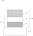
- a wide gap semiconductor device has a wide gap semiconductor layer 10 and a metal electrode 20 disposed on the wide gap semiconductor layer 10.
- the metal electrode 20 may have a monocrystalline layer 21 having a hexagonal close-packed (HCP) structure in an interface region between the metal electrode 20 and the wide gap semiconductor layer 10 (on the back side of the metal electrode 20).
- the monocrystalline layer 21 may have a specific element-containing region 22 containing oxygen (O), sulfur (S), phosphorus (P), or selenium (Se) in the interface region between the metal electrode 20 and the wide gap semiconductor layer 10.
- One or more elements of O, S, P, and Se, but typically O, can be included in the specific element-containing region 22.
- Examples of the wide gap semiconductor include SiC and GaN.
- the upper side of Fig. 1 is the front side of the wide gap semiconductor device, and the lower side is the back side of the wide gap semiconductor device.
- the metal electrode 20 of this embodiment constitutes a Schottky electrode.
- the monocrystalline layer 21 may be titanium (Ti), cadmium (Cd), hafnium (Hf), magnesium (Mg), zirconium (Zr), or scandium (Sc) or may contain two or more of these metals.
- Ti is typically used, and hereinafter mainly described is an aspect in which Ti is used. Note that Cd, Hf, Mg, Zr, and Sc derive results similar to Ti because those metals have a hexagonal close-packed (HCP) crystal structure and a lattice constant close to that of SiC.
- the specific element-containing region 22 of the monocrystalline layer 21 may contain O, S, P, or Se.
- the specific element-containing region 22 of the monocrystalline layer 21 may contain O.
- a total atomic concentration of O, S, P, and Se in the specific element-containing region 22 may be 7% to 33%.
- the atomic concentration herein is "total concentration.”
- a total atomic concentration of the elements is 7% to 33%.
- an atomic concentration of the element is 7% to 33%.
- O, S, P, and Se O is typically used, and hereinafter mainly described is a case where O is used.
- the theoretical upper limit of concentration of atoms such as O, S, P, and Se which can be inserted while maintaining an HCP structure is 33%.
- the upper limit of atomic concentration is set to 33%. As long as the HCP structure is maintained, no abnormal leakage current occurs. In contrast, when an impurity concentration is 33% or more as in TiO 2 employed in the above Non-Patent Document, it is difficult for the monocrystalline layer 21 to maintain its original hexagonal close-packed (HCP) crystal structure, which causes an abnormal leakage current.
- HCP hexagonal close-packed
- results of first-principle calculation show that S, P, and Se are all chemically bonded to Ti or the like and that, in a case where those elements have an identical structure, a relatively large number of valence electrons causes an increase in Fermi energy. Accordingly, S, P, and Se all derive results similar to O. For example, comparing Ti 6 O and Ti 2 S, assuming that Ti 6 O and Ti 2 S have an identical structure, Ti 2 S is higher in Fermi energy because the number of valence electrons is relatively larger. Even in a case where Ti 6 O and Ti 2 S do not have an identical structures, it is possible to obtain a similar effect as long as Ti 6 O and Ti 2 S stably have similar structures.
- the specific element-containing region 22 may be located within a distance from 11 nm to 37 nm in a thickness direction from an interface between the metal electrode 20 and the wide gap semiconductor layer 10. In an aspect shown in Fig. 1 , the specific element-containing region 22 may have a thickness of from 11 nm to 37 nm from the interface between the metal electrode 20 and the wide gap semiconductor layer 10.
- the specific element-containing region 22 contains a significant amount of any of O, S, P, and Se in an atomic state, typically having an atomic concentration of 5% or more.
- the specific element-containing region 22 may be disposed over the entire surface in the in-plane direction.
- the metal electrode 20 may have a polycrystalline layer 29 on the front side opposite the wide gap semiconductor layer 10. Between the specific element-containing region 22 and the polycrystalline layer 29, there may be disposed a monocrystalline main layer 25 which contains no specific element or a small amount of specific elements as compared with the specific element-containing region 22.
- the monocrystalline main layer 25 and the specific element-containing region 22 may constitute the monocrystalline layer 21.
- the specific element-containing region 22 may be a high concentration specific element-containing region.
- the metal electrode 20 may have a low concentration specific element-containing region which is disposed on a side of the high concentration specific element-containing region opposite the wide gap semiconductor layer 10 (the upper side in Fig. 1 ) and which has a lower oxygen concentration than the oxygen concentration in the interface region.
- the monocrystalline main layer 25 has a low concentration specific element-containing region.
- the metal electrode 20 may have a hydrogen-containing region on a side opposite the wide gap semiconductor layer 10.
- the polycrystalline layer 29 may have a hydrogen-containing region, and in this case, the hydrogen-containing region is disposed inside the polycrystalline layer 29. All or part of the polycrystalline layer 29 may be the hydrogen-containing region.
- a TiO 2 -containing layer is disposed on the surface of the metal electrode 20 because Ti is easily oxidized (see Fig. 7B ).
- Fig. 2 illustrates I-V waveforms of SiC-SBDs (Schottky barrier diode) using an aspect in which the wide gap semiconductor layer 10 is SiC, the metal electrode 20 is Ti, and the specific element-containing region 22 contains O atoms.
- Comparative Example 1 shows an aspect in which the specific element-containing region 22 does not contain a significant amount of O atoms
- Comparative Example 2 shows an aspect in which the specific element-containing region 22 contains TiO 2
- Example 1 shows an aspect in which the specific element-containing region 22 contains a significant amount of O atoms.
- the threshold voltage is high.
- an abnormal leakage current occurs at 0 to 0.2 V.
- no abnormal leakage current as in Comparative Example 2 occurs and the threshold voltage can be reduced.
- Fig. 3 shows results obtained by the first-principle calculation, showing the relation between lattice constant C-axial length and Fermi energy in an aspect where the wide gap semiconductor layer 10 is SiC, the metal electrode 20 is Ti, the specific element-containing region 22 contains O atoms, and the content of O atoms in the specific element-containing region 22 is increased. It can be confirmed that an increase in concentration of O atoms in an interface region between Ti and SiC increases the Fermi energy and decreases ⁇ B (Schottky barrier height).
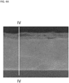
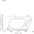
- Figs. 4A and 4B show results of composition analysis on Ti and O performed by energy-dispersive X-ray spectroscopy (EDX) with STEM and results of analysis on H performed with a glow discharge optical emission spectrometer (GD-OES), employing the aspect in which the wide gap semiconductor layer 10 is SiC, the metal electrode 20 is Ti, and the specific element-containing region 22 contains O atoms.
- a cut line of energy-dispersive X-ray spectroscopy (EDX) is indicated by straight line IV-IV in Fig. 4A .
- a depth of 0 um in Fig. 4B is an interface on the front side of the metal electrode 20, and a depth of 0.15 um is an interface between Ti and SiC.
- Table 1 shows sites, crystal structures, compositions, and crystal orientations obtained from Fig. 4B .
- the specific element-containing region 22 is located within a distance of 30 nm or less in the thickness direction from the interface between the metal electrode 20 and the wide gap semiconductor layer 10, and the hydrogen-containing region is separated from the interface between the metal electrode 20 and the wide gap semiconductor layer 10 by 80 nm or more in the thickness direction.
- Figs. 5A and 5B illustrate an aspect in which the wide gap semiconductor layer 10 is SiC and the metal electrode 20 is Ti without the specific element-containing region 22 (Comparative Example 1).
- Fig. 5A corresponds to Fig. 4A
- Fig. 5B corresponds to Fig. 4B .
- a cut line of energy-dispersive X-ray spectroscopy (EDX) is indicated by straight line V-V in Fig. 5A .
- no "bump" (see a depth ranging from 0.13 to 0.15 um in Fig. 4B ) having an oxygen concentration corresponding to the Ti-O layer was detected at an interface between a SiC layer and a Ti layer.
- the oxygen concentration around the interface between the SiC layer and the Ti layer is 6.6%, which is below about 10%, the lower limit of detection.
- the EELS signal waveform of Ti in the Ti-O layer, or the specific element-containing region 22 is similar to the EELS signal waveform of monocrystalline Ti epitaxially grown on SiC in Comparative Example 1.
- O atoms are in Ti lattice of the Ti-O layer, or the specific element-containing region 22, and Ti and O are not covalently bonded.
- the oxygen concentration increases to 40% on the front side and Ti and O are covalently bonded, causing a shift in EELS signal waveform.
- O atoms are in Ti lattice of the Ti-O layer, or the specific element-containing region 22, and Ti and O are not covalently bonded.
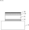
- the metal electrode 20 being Ti is disposed on the wide gap semiconductor layer 10 which is SiC(see Fig. 7A ). Since Ti is easily oxidized, the surface of the metal electrode 20 being Ti comes into contact with oxygen, thereby forming a layer being TiO 2 (TiO 2 layer) 30.
- H 2 gas or H 2 gas diluted with Ar H 2 gas flow rate of 1 to 20%
- H 2 gas flow rate of 1 to 20% is supplied, followed by annealing at 300 to 600 °C.
- a Ti-H layer is formed on the front side by the supplied H 2 gas.
- oxygen originally included in the metal electrode 20 being Ti is pushed into a Ti/SiC interface to form a Ti-O layer, or the specific element-containing region 22.
- H atoms of the supplied H 2 gas penetrate into Ti through defects or the like in the TiO 2 layer.
- the surface of Ti is oxidized by residual oxygen and moisture in the chamber. It is believed that oxygen and part of O atoms derived from moisture in the chamber also penetrate into the inside through grain boundaries of polycrystalline Ti on the front side, thereby increasing the Ti-O layer, or the specific element-containing region 22. More specifically, it is believed that oxygen remaining in the chamber is separated into O atoms, enters into the metal electrode 20 being Ti, and oxides the surface of the metal electrode 20 or moves to the Ti/SiC interface to increase the Ti-O layer (indicated by reference numeral 79 in Fig. 7B ). In addition, it is believed that moisture (H 2 O) remaining in the chamber is separated into H and OH, and OH enters the metal electrode 20 being Ti and oxides the surface or moves to the Ti/SiC interface to increase the Ti-O layer 22.
- Example 1 annealing was performed at 350 °C or higher in the presence of H 2 gas.
- the inventors have found that it is possible to reduce ⁇ B without causing an abnormal leakage current in an aspect where the metal electrode 20 has the monocrystalline layer 21 having the hexagonal close-packed (HCP) structure in the interface region between the metal electrode 20 and the wide gap semiconductor layer 10 and the monocrystalline layer 21 has the specific element-containing region 22 containing O, S, P, or Se (see Fig. 2 ).
- HCP hexagonal close-packed
- the metal electrode 20 is Ti and the specific element-containing region 22 contains O, S, P, or Se or in a case where the metal electrode 20 is Cd, Hf, Mg, Zr, or Sc and the specific element-containing region 22 contains O, it is possible to reduce ⁇ B more reliably without causing an abnormal leakage current.
- the total atomic concentration of O, S, P, and Se in the specific element-containing region 22 is 7% to 33%. This is because introduction of O, S, and P in an amount larger than 33% makes it difficult for the metal electrode 20 to maintain the hexagonal close-packed (HCP) structure and causes an abnormal leakage current.
- the specific element-containing region 22 is disposed over the entire surface in the in-plane direction, but the invention is not limited thereto.
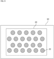
- specific element-containing regions 22 are scattered like islands in the in-plane direction.
- Fig. 9 shows a plan view of only the specific element-containing regions 22 inside the metal electrode 20.
- Such island-like specific element-containing regions 22 can be generated by annealing using H 2 gas diluted with Ar. In diluting with Ar, H 2 does not push oxygen or the like so strongly, which may form the island-like specific element-containing regions 22.
Landscapes
- Electrodes Of Semiconductors (AREA)
- Bipolar Transistors (AREA)
- Junction Field-Effect Transistors (AREA)
Abstract
Description
- The present invention relates to a wide gap semiconductor device having a wide gap semiconductor layer and a metal electrode disposed on the wide gap semiconductor layer.
- In the related art, there is known a wide gap semiconductor device employing SiC or the like (see, for example,
JP 2015-56543 A - For example, citing SiC as a wide gap semiconductor device, ϕB of an N-type SiC-SBD (Schottky barrier diode) is typically controlled by a Schottky electrode, and Ti, Ni, Pt, and the like are used as the Schottky electrode of the N-type SiC-SBD. Among these metals, Ti is known to have the smallest ϕB, and most of commercially available N-type SiC-SBDs use Ti as a Schottky electrode.
- With reference to Non-Patent Document (Extended Abstracts of the 2013 International Conference on Solid State Devices and Materials, Fukuoka, 2013, pp 468-469), the inventors of this application have studied a configuration having a TiO2 layer at an interface as a technique for reducing ϕB and have found that such a configuration is impractical due to an abnormal leakage current, that is, a current value becomes larger than a theoretically expected value in a low voltage range of a forward voltage.
- In view of the problem, the present invention provides a wide gap semiconductor device capable of reducing ϕB without causing an abnormal leakage current.
- A wide gap semiconductor device according to the present invention may comprise:
- a wide gap semiconductor layer; and
- a metal electrode disposed on the wide gap semiconductor layer,
- wherein the metal electrode has a monocrystalline layer having a hexagonal close-packed (HCP) structure in an interface region between the metal electrode and the wide gap semiconductor layer, and
- wherein the monocrystalline layer has a specific element-containing region containing O, S, P or Se.
- In the wide gap semiconductor device according to the present invention,
- the metal electrode may be Ti, Cd, Hf, Mg, Zr or Sc,
- the specific element-containing region may contain O, S, P or Se in a case where the metal electrode is Ti, and the specific element-containing region may contain O in a case where the metal electrode is Cd, Hf, Mg, Zr or Sc.
- In the wide gap semiconductor device according to the present invention,
a total atomic concentration of O, S, P and Se in the specific element-containing region may be 7% to 33%. - In the wide gap semiconductor device according to the present invention,
the specific element-containing region may be located within a distance from 11 nm to 37 nm in a thickness direction from an interface between the metal electrode and the wide gap semiconductor layer. - In the wide gap semiconductor device according to the present invention,
specific element-containing regions may be scattered like islands in an in-plane direction. - In the wide gap semiconductor device according to the present invention,
- the specific element-containing region may be a high concentration specific element-containing region, and
- the metal electrode may have a low concentration specific element-containing region which is disposed on the high concentration specific element-containing region opposite the wide gap semiconductor layer and which has a lower oxygen concentration than an oxygen concentration in the interface region.
- In the wide gap semiconductor device according to the present invention,
the metal electrode may have a polycrystalline layer on a side opposite the wide gap semiconductor layer. - In the wide gap semiconductor device according to the present invention,
the metal electrode may have a hydrogen-containing region on a side opposite the wide gap semiconductor layer. - It is possible to reduce ϕB without causing an abnormal leakage current, when an aspect where the metal electrode has the monocrystalline layer having the hexagonal close-packed (HCP) structure in the interface region between the metal electrode and the wide gap semiconductor layer and the monocrystalline layer has the specific element-containing region containing O, S, P, or Se is employed in the present invention.
-
-
Fig. 1 is a longitudinal sectional view showing a wide gap semiconductor device according to a first embodiment of the invention. -
Fig. 2 is a graph showing the relation between VF (V) and IF (A) in Example 1, Comparative Example 1, and Comparative Example 2. -
Fig. 3 is a graph showing the relation between C-axis lattice constant (nm) and Fermi energy (eV/atm). -
Fig. 4A is an image obtained by capturing a metal electrode in Example of the invention with scanning equivalent electron microscope (STEM). -
Fig. 4B is a graph showing amounts of Ti, O, and H included in the metal electrode in Example of the invention. -
Fig. 5A is an image obtained by capturing a metal electrode in Comparative Example 1 with STEM. -
Fig. 5B is a graph showing amounts of Ti, O, and H included in the metal electrode in Comparative Example 1. -
Fig. 6 is a graph showing EELS signal waveforms of Ti in Example 1 and Comparative Example 1 and images captured with STEM. -
Fig. 7A is a view showing an example of a method for manufacturing a wide gap semiconductor device according to the first embodiment of the invention. -
Fig. 7B is a view followingFig. 7A , showing an example of the method for manufacturing a wide gap semiconductor device according to the first embodiment of the invention. -
Fig. 8 is a longitudinal sectional view showing a wide gap semiconductor device according to a second embodiment of the invention. -
Fig. 9 is a plan view showing specific element-containing regions scattered like islands in the second embodiment of the invention. - As shown in
Fig. 1 , a wide gap semiconductor device according to this embodiment has a widegap semiconductor layer 10 and ametal electrode 20 disposed on the widegap semiconductor layer 10. Themetal electrode 20 may have amonocrystalline layer 21 having a hexagonal close-packed (HCP) structure in an interface region between themetal electrode 20 and the wide gap semiconductor layer 10 (on the back side of the metal electrode 20). Themonocrystalline layer 21 may have a specific element-containingregion 22 containing oxygen (O), sulfur (S), phosphorus (P), or selenium (Se) in the interface region between themetal electrode 20 and the widegap semiconductor layer 10. One or more elements of O, S, P, and Se, but typically O, can be included in the specific element-containingregion 22. Examples of the wide gap semiconductor include SiC and GaN. The upper side ofFig. 1 is the front side of the wide gap semiconductor device, and the lower side is the back side of the wide gap semiconductor device. Themetal electrode 20 of this embodiment constitutes a Schottky electrode. - In an aspect, the
monocrystalline layer 21 may be titanium (Ti), cadmium (Cd), hafnium (Hf), magnesium (Mg), zirconium (Zr), or scandium (Sc) or may contain two or more of these metals. Among these metals, Ti is typically used, and hereinafter mainly described is an aspect in which Ti is used. Note that Cd, Hf, Mg, Zr, and Sc derive results similar to Ti because those metals have a hexagonal close-packed (HCP) crystal structure and a lattice constant close to that of SiC. - In a case where the
monocrystalline layer 21 is Ti, the specific element-containingregion 22 of themonocrystalline layer 21 may contain O, S, P, or Se. In a case where themonocrystalline layer 21 is Cd, Hf, Mg, Zr, or Sc, the specific element-containingregion 22 of themonocrystalline layer 21 may contain O. - A total atomic concentration of O, S, P, and Se in the specific element-containing
region 22 may be 7% to 33%. The atomic concentration herein is "total concentration." In a case where the specific element-containingregion 22 includes two or more of O, S, P, and Se, a total atomic concentration of the elements is 7% to 33%. In a case where the specific element-containingregion 22 includes one of O, S, P, and Se, an atomic concentration of the element is 7% to 33%. Among O, S, P, and Se, O is typically used, and hereinafter mainly described is a case where O is used. The theoretical upper limit of concentration of atoms such as O, S, P, and Se which can be inserted while maintaining an HCP structure is 33%. This is why the upper limit of atomic concentration is set to 33%. As long as the HCP structure is maintained, no abnormal leakage current occurs. In contrast, when an impurity concentration is 33% or more as in TiO2 employed in the above Non-Patent Document, it is difficult for themonocrystalline layer 21 to maintain its original hexagonal close-packed (HCP) crystal structure, which causes an abnormal leakage current. - Similarly to O, results of first-principle calculation show that S, P, and Se are all chemically bonded to Ti or the like and that, in a case where those elements have an identical structure, a relatively large number of valence electrons causes an increase in Fermi energy. Accordingly, S, P, and Se all derive results similar to O. For example, comparing Ti6O and Ti2S, assuming that Ti6O and Ti2S have an identical structure, Ti2S is higher in Fermi energy because the number of valence electrons is relatively larger. Even in a case where Ti6O and Ti2S do not have an identical structures, it is possible to obtain a similar effect as long as Ti6O and Ti2S stably have similar structures.
- The specific element-containing
region 22 may be located within a distance from 11 nm to 37 nm in a thickness direction from an interface between themetal electrode 20 and the widegap semiconductor layer 10. In an aspect shown inFig. 1 , the specific element-containingregion 22 may have a thickness of from 11 nm to 37 nm from the interface between themetal electrode 20 and the widegap semiconductor layer 10. The specific element-containingregion 22 contains a significant amount of any of O, S, P, and Se in an atomic state, typically having an atomic concentration of 5% or more. - Unlike the following second embodiment, the specific element-containing
region 22 may be disposed over the entire surface in the in-plane direction. - The
metal electrode 20 may have apolycrystalline layer 29 on the front side opposite the widegap semiconductor layer 10. Between the specific element-containingregion 22 and thepolycrystalline layer 29, there may be disposed a monocrystallinemain layer 25 which contains no specific element or a small amount of specific elements as compared with the specific element-containingregion 22. The monocrystallinemain layer 25 and the specific element-containingregion 22 may constitute themonocrystalline layer 21. - The specific element-containing
region 22 may be a high concentration specific element-containing region. Themetal electrode 20 may have a low concentration specific element-containing region which is disposed on a side of the high concentration specific element-containing region opposite the wide gap semiconductor layer 10 (the upper side inFig. 1 ) and which has a lower oxygen concentration than the oxygen concentration in the interface region. In an aspect of this embodiment, the monocrystallinemain layer 25 has a low concentration specific element-containing region. - The
metal electrode 20 may have a hydrogen-containing region on a side opposite the widegap semiconductor layer 10. Thepolycrystalline layer 29 may have a hydrogen-containing region, and in this case, the hydrogen-containing region is disposed inside thepolycrystalline layer 29. All or part of thepolycrystalline layer 29 may be the hydrogen-containing region. In a case where themetal electrode 20 is Ti, a TiO2-containing layer is disposed on the surface of themetal electrode 20 because Ti is easily oxidized (seeFig. 7B ). -
Fig. 2 illustrates I-V waveforms of SiC-SBDs (Schottky barrier diode) using an aspect in which the widegap semiconductor layer 10 is SiC, themetal electrode 20 is Ti, and the specific element-containingregion 22 contains O atoms. Comparative Example 1 shows an aspect in which the specific element-containingregion 22 does not contain a significant amount of O atoms, Comparative Example 2 shows an aspect in which the specific element-containingregion 22 contains TiO2, and Example 1 shows an aspect in which the specific element-containingregion 22 contains a significant amount of O atoms. As can be seen in the aspect of Comparative Example 1, the threshold voltage is high. As can be seen in the aspect of Comparative Example 2, an abnormal leakage current occurs at 0 to 0.2 V. In contrast, in the aspect of Example 1, no abnormal leakage current as in Comparative Example 2 occurs and the threshold voltage can be reduced. -
Fig. 3 shows results obtained by the first-principle calculation, showing the relation between lattice constant C-axial length and Fermi energy in an aspect where the widegap semiconductor layer 10 is SiC, themetal electrode 20 is Ti, the specific element-containingregion 22 contains O atoms, and the content of O atoms in the specific element-containingregion 22 is increased. It can be confirmed that an increase in concentration of O atoms in an interface region between Ti and SiC increases the Fermi energy and decreases ϕB (Schottky barrier height). -
Figs. 4A and4B show results of composition analysis on Ti and O performed by energy-dispersive X-ray spectroscopy (EDX) with STEM and results of analysis on H performed with a glow discharge optical emission spectrometer (GD-OES), employing the aspect in which the widegap semiconductor layer 10 is SiC, themetal electrode 20 is Ti, and the specific element-containingregion 22 contains O atoms. A cut line of energy-dispersive X-ray spectroscopy (EDX) is indicated by straight line IV-IV inFig. 4A . A depth of 0 um inFig. 4B is an interface on the front side of themetal electrode 20, and a depth of 0.15 um is an interface between Ti and SiC. - The following Table 1 shows sites, crystal structures, compositions, and crystal orientations obtained from
Fig. 4B . In the aspect shown inFig. 4B , the specific element-containingregion 22 is located within a distance of 30 nm or less in the thickness direction from the interface between themetal electrode 20 and the widegap semiconductor layer 10, and the hydrogen-containing region is separated from the interface between themetal electrode 20 and the widegap semiconductor layer 10 by 80 nm or more in the thickness direction.[Table 1] SITE CRYSTAL STRUCTURE COMPOSITION CRYSTAL ORIENTATION SiC LAYER 4H-SiC Si, C 4° Ti-O LAYER (0 TO 30 nm FROM INTERFACE) MONOCRYSTALLINE HEXAGONAL CLOSE-PACKED Ti Ti, O 3° , 3° Ti-H LAYER (80 nm OR MORE FROM INTERFACE) POLYCRYSTALLINE Ti Ti, H, O 3° , 11° , 12° , -1° , 3° , -1° - As shown above, only components having a crystal orientation at "3°" are detected in the Ti-O layer adjacent to the SiC layer. This result shows that O is contained in the monocrystalline hexagonal close-packed Ti. In addition, a plurality of crystal orientations is detected on a side opposite the SiC layer, which shows that polycrystalline Ti is formed and that the polycrystalline Ti contains H. Since Ti is relatively and easily oxidized, Ti is oxidized instantaneously at the time of cross-sectional processing for analysis. Accordingly, the lower limit of O detection in the Ti layer or the
metal electrode 20 is about 10%, which is larger than the lower limit of O detection in the SiC layer, which is about 0%. It should be noted that a high oxygen concentration inside Ti inFig. 4B is caused by the oxidizability of Ti. -
Figs. 5A and5B illustrate an aspect in which the widegap semiconductor layer 10 is SiC and themetal electrode 20 is Ti without the specific element-containing region 22 (Comparative Example 1).Fig. 5A corresponds toFig. 4A , andFig. 5B corresponds toFig. 4B . A cut line of energy-dispersive X-ray spectroscopy (EDX) is indicated by straight line V-V inFig. 5A . UnlikeFig. 4B , no "bump" (see a depth ranging from 0.13 to 0.15 um inFig. 4B ) having an oxygen concentration corresponding to the Ti-O layer was detected at an interface between a SiC layer and a Ti layer. The oxygen concentration around the interface between the SiC layer and the Ti layer is 6.6%, which is below about 10%, the lower limit of detection. - As shown in
Fig. 6 , in the aspect of Example 1, the EELS signal waveform of Ti in the Ti-O layer, or the specific element-containingregion 22, is similar to the EELS signal waveform of monocrystalline Ti epitaxially grown on SiC in Comparative Example 1. As can be seen from this result, O atoms are in Ti lattice of the Ti-O layer, or the specific element-containingregion 22, and Ti and O are not covalently bonded. In Example 1, the oxygen concentration increases to 40% on the front side and Ti and O are covalently bonded, causing a shift in EELS signal waveform. As can be seen from this result, O atoms are in Ti lattice of the Ti-O layer, or the specific element-containingregion 22, and Ti and O are not covalently bonded. - Hereinafter described is an example of a manufacturing method according to an aspect of this embodiment. The manufacturing method will be described using an aspect in which the wide
gap semiconductor layer 10 is SiC and themetal electrode 20 is Ti. - First, the
metal electrode 20 being Ti is disposed on the widegap semiconductor layer 10 which is SiC(seeFig. 7A ). Since Ti is easily oxidized, the surface of themetal electrode 20 being Ti comes into contact with oxygen, thereby forming a layer being TiO2 (TiO2 layer) 30. - Next, after vacuum is drawn inside a chamber, H2 gas or H2 gas diluted with Ar (H2 gas flow rate of 1 to 20%) is supplied, followed by annealing at 300 to 600 °C. A Ti-H layer is formed on the front side by the supplied H2 gas. Along with the formation of the Ti-H layer, it is believed that oxygen originally included in the
metal electrode 20 being Ti is pushed into a Ti/SiC interface to form a Ti-O layer, or the specific element-containingregion 22. Furthermore, it is believed that H atoms of the supplied H2 gas penetrate into Ti through defects or the like in the TiO2 layer. - At this time, the surface of Ti is oxidized by residual oxygen and moisture in the chamber. It is believed that oxygen and part of O atoms derived from moisture in the chamber also penetrate into the inside through grain boundaries of polycrystalline Ti on the front side, thereby increasing the Ti-O layer, or the specific element-containing
region 22. More specifically, it is believed that oxygen remaining in the chamber is separated into O atoms, enters into themetal electrode 20 being Ti, and oxides the surface of themetal electrode 20 or moves to the Ti/SiC interface to increase the Ti-O layer (indicated by reference numeral 79 inFig. 7B ). In addition, it is believed that moisture (H2O) remaining in the chamber is separated into H and OH, and OH enters themetal electrode 20 being Ti and oxides the surface or moves to the Ti/SiC interface to increase the Ti-O layer 22. - In this manner, there is produced a wide gap semiconductor device having the specific element-containing
region 22 being the Ti-O layer at the Ti/SiC interface and having the hydrogen-containing region on the front side. In Example 1 described above, annealing was performed at 350 °C or higher in the presence of H2 gas. - Hereinafter, an effect obtained from this embodiment having the above configuration will be described focusing on those not mentioned yet.
- The inventors have found that it is possible to reduce ϕB without causing an abnormal leakage current in an aspect where the
metal electrode 20 has themonocrystalline layer 21 having the hexagonal close-packed (HCP) structure in the interface region between themetal electrode 20 and the widegap semiconductor layer 10 and themonocrystalline layer 21 has the specific element-containingregion 22 containing O, S, P, or Se (seeFig. 2 ). - In particular, in a case where the
metal electrode 20 is Ti and the specific element-containingregion 22 contains O, S, P, or Se or in a case where themetal electrode 20 is Cd, Hf, Mg, Zr, or Sc and the specific element-containingregion 22 contains O, it is possible to reduce ϕB more reliably without causing an abnormal leakage current. - In order to obtain the effect of reducing ϕB more reliably without causing an abnormal leakage current, it is beneficial that the total atomic concentration of O, S, P, and Se in the specific element-containing
region 22 is 7% to 33%. This is because introduction of O, S, and P in an amount larger than 33% makes it difficult for themetal electrode 20 to maintain the hexagonal close-packed (HCP) structure and causes an abnormal leakage current. - Next, a second embodiment of the invention will be described.
- In the first embodiment, the specific element-containing
region 22 is disposed over the entire surface in the in-plane direction, but the invention is not limited thereto. In an aspect of this embodiment, as shown inFigs. 8 and9 , specific element-containingregions 22 are scattered like islands in the in-plane direction. It should be noted that in order to show the specific element-containingregions 22 scattered like islands,Fig. 9 shows a plan view of only the specific element-containingregions 22 inside themetal electrode 20. Such island-like specific element-containingregions 22 can be generated by annealing using H2 gas diluted with Ar. In diluting with Ar, H2 does not push oxygen or the like so strongly, which may form the island-like specific element-containingregions 22. - Other configurations are similar to those described in the first embodiment. In the second embodiment, the same or similar members and the like as those in the first embodiment are denoted by the same reference numerals, and the description thereof will be omitted.
- According to this embodiment, it is possible to obtain an effect similar to one achieved by the first embodiment. That is, even in an aspect in this embodiment where the specific element-containing
regions 22 containing O, S, P, or Se are scattered like islands in the in-plane direction, it is possible to reduce ϕB without causing an abnormal leakage current when the specific element-containingregions 22 have a total atomic concentration of 7% to 33%. - The description of each embodiment and the disclosure of the figures described above are merely examples for describing the invention described in the claims, and the invention described in the claims is not limited by the description of the embodiments or the disclosure of the figures described above. In addition, the description of the claims as originally filed is merely an example, and the description of the claims can be appropriately changed based on the description of the specification, the figures, and the like.
-
- 10
- Wide gap semiconductor layer
- 20
- Metal electrode
- 21
- Monocrystalline layer
- 22
- Specific element-containing region
- 25
- Monocrystalline main layer
- 29
- Polycrystalline layer
- 30
- layer being TiO2 (TiO2 layer)
Claims (8)
- A wide gap semiconductor device comprising:a wide gap semiconductor layer; anda metal electrode disposed on the wide gap semiconductor layer,wherein the metal electrode has a monocrystalline layer having a hexagonal close-packed (HCP) structure in an interface region between the metal electrode and the wide gap semiconductor layer, andwherein the monocrystalline layer has a specific element-containing region containing O, S, P or Se.
- The wide gap semiconductor device according to claim 1,wherein the metal electrode is Ti, Cd, Hf, Mg, Zr or Sc,wherein the specific element-containing region contains O, S, P or Se in a case where the metal electrode is Ti, and the specific element-containing region contains O in a case where the metal electrode is Cd, Hf, Mg, Zr or Sc.
- The wide gap semiconductor device according to claim 1 or 2,
wherein a total atomic concentration of O, S, P and Se in the specific element-containing region is 7% to 33%. - The wide gap semiconductor device according to any one of claims 1 to 3,
wherein the specific element-containing region is located within a distance from 11 nm to 37 nm in a thickness direction from an interface between the metal electrode and the wide gap semiconductor layer. - The wide gap semiconductor device according to any one of claims 1 to 4,
wherein specific element-containing regions are scattered like islands in an in-plane direction. - The wide gap semiconductor device according to any one of claims 1 to 5,wherein the specific element-containing region is a high concentration specific element-containing region, andwherein the metal electrode has a low concentration specific element-containing region which is disposed on the high concentration specific element-containing region opposite the wide gap semiconductor layer and which has a lower oxygen concentration than an oxygen concentration in the interface region.
- The wide gap semiconductor device according to any one of claims 1 to 6,
wherein the metal electrode has a polycrystalline layer on a side opposite the wide gap semiconductor layer. - The wide gap semiconductor device according to any one of claims 1 to 7,
wherein the metal electrode has a hydrogen-containing region on a side opposite the wide gap semiconductor layer.
Applications Claiming Priority (2)
| Application Number | Priority Date | Filing Date | Title |
|---|---|---|---|
| JP2020143284 | 2020-08-27 | ||
| PCT/JP2021/031066 WO2022045160A1 (en) | 2020-08-27 | 2021-08-25 | Wide gap semiconductor device |
Publications (2)
| Publication Number | Publication Date |
|---|---|
| EP4207308A1 true EP4207308A1 (en) | 2023-07-05 |
| EP4207308A4 EP4207308A4 (en) | 2024-09-04 |
Family
ID=80355261
Family Applications (1)
| Application Number | Title | Priority Date | Filing Date |
|---|---|---|---|
| EP21861584.7A Pending EP4207308A4 (en) | 2020-08-27 | 2021-08-25 | LARGE GAP SEMICONDUCTOR ARRANGEMENT |
Country Status (6)
| Country | Link |
|---|---|
| US (1) | US12363927B2 (en) |
| EP (1) | EP4207308A4 (en) |
| JP (1) | JP7369302B2 (en) |
| CN (1) | CN115989584B (en) |
| TW (1) | TWI777752B (en) |
| WO (1) | WO2022045160A1 (en) |
Families Citing this family (2)
| Publication number | Priority date | Publication date | Assignee | Title |
|---|---|---|---|---|
| WO2022215471A1 (en) * | 2021-04-05 | 2022-10-13 | ローム株式会社 | Semiconductor device and method for manufacturing semiconductor device |
| EP4718988A1 (en) * | 2024-09-25 | 2026-04-01 | Hitachi Energy Ltd | Method for producing a first contact layer and a second contact layer on a power semiconductor body, and power semiconductor device |
Family Cites Families (15)
| Publication number | Priority date | Publication date | Assignee | Title |
|---|---|---|---|---|
| JP3557011B2 (en) * | 1995-03-30 | 2004-08-25 | 株式会社東芝 | Semiconductor light emitting device and manufacturing method thereof |
| JP3361062B2 (en) | 1998-09-17 | 2003-01-07 | 株式会社東芝 | Semiconductor device |
| US8183594B2 (en) * | 2007-03-15 | 2012-05-22 | National University Corporation Toyohashi University Of Technology | Laminar structure on a semiconductor substrate |
| JP4645641B2 (en) | 2007-12-03 | 2011-03-09 | 富士電機システムズ株式会社 | Method for manufacturing SiC Schottky diode |
| JP5453867B2 (en) | 2009-03-24 | 2014-03-26 | 株式会社デンソー | Silicon carbide semiconductor device having Schottky barrier diode and method for manufacturing the same |
| JP5598015B2 (en) | 2010-02-23 | 2014-10-01 | 株式会社デンソー | Silicon carbide semiconductor device having Schottky barrier diode and method for manufacturing the same |
| TW201137975A (en) * | 2010-04-19 | 2011-11-01 | Sumitomo Electric Industries | Silicon carbide semiconductor device and its manufacturing method |
| US9887139B2 (en) * | 2011-12-28 | 2018-02-06 | Infineon Technologies Austria Ag | Integrated heterojunction semiconductor device and method for producing an integrated heterojunction semiconductor device |
| JP2014053393A (en) | 2012-09-06 | 2014-03-20 | Sumitomo Electric Ind Ltd | Wide gap semiconductor device and method for manufacturing the same |
| JP6244763B2 (en) | 2013-09-12 | 2017-12-13 | 住友電気工業株式会社 | Silicon carbide semiconductor device |
| JP6242724B2 (en) | 2014-03-20 | 2017-12-06 | 株式会社東芝 | Semiconductor device and manufacturing method thereof |
| JP6584966B2 (en) | 2016-01-12 | 2019-10-02 | 株式会社東芝 | Semiconductor device, semiconductor device manufacturing method, inverter circuit, drive device, vehicle, and elevator |
| JP6667712B2 (en) * | 2017-02-14 | 2020-03-18 | 三菱電機株式会社 | Power semiconductor device |
| JP6977465B2 (en) | 2017-10-06 | 2021-12-08 | 株式会社デンソー | Manufacturing method of semiconductor device |
| JP2020092321A (en) * | 2018-12-05 | 2020-06-11 | 太陽誘電株式会社 | Acoustic wave device and its manufacturing method, filter and multiplexer |
-
2021
- 2021-08-25 US US18/008,657 patent/US12363927B2/en active Active
- 2021-08-25 JP JP2022545650A patent/JP7369302B2/en active Active
- 2021-08-25 WO PCT/JP2021/031066 patent/WO2022045160A1/en not_active Ceased
- 2021-08-25 EP EP21861584.7A patent/EP4207308A4/en active Pending
- 2021-08-25 CN CN202180052727.2A patent/CN115989584B/en active Active
- 2021-08-27 TW TW110131789A patent/TWI777752B/en active
Also Published As
| Publication number | Publication date |
|---|---|
| WO2022045160A1 (en) | 2022-03-03 |
| JPWO2022045160A1 (en) | 2022-03-03 |
| CN115989584B (en) | 2026-03-06 |
| US12363927B2 (en) | 2025-07-15 |
| US20230246111A1 (en) | 2023-08-03 |
| JP7369302B2 (en) | 2023-10-25 |
| EP4207308A4 (en) | 2024-09-04 |
| TWI777752B (en) | 2022-09-11 |
| TW202213713A (en) | 2022-04-01 |
| CN115989584A (en) | 2023-04-18 |
Similar Documents
| Publication | Publication Date | Title |
|---|---|---|
| US11699748B2 (en) | Normally-off HEMT transistor with selective generation of 2DEG channel, and manufacturing method thereof | |
| US11227942B2 (en) | Semiconductor device, method for manufacturing the same, power circuit, and computer | |
| EP1633004B1 (en) | Guard ring for semiconductor devices | |
| EP2421045A1 (en) | SECOND SCHOTTKY CONTACT METAL LAYER TO IMPROVE GaN SCHOTTKY DIODE PERFORMANCE | |
| CN108735810A (en) | The manufacturing method of semiconductor devices and semiconductor devices | |
| US10236353B2 (en) | Semiconductor device, power supply circuit, and computer | |
| US20170077238A1 (en) | Semiconductor device and method of manufacturing the same | |
| US10038070B2 (en) | Nitride semiconductor device | |
| EP2920817A1 (en) | Gan-based schottky diode having partially recessed anode | |
| US11552170B2 (en) | Semiconductor device including current spread region | |
| JP2011210751A (en) | Group iii nitride semiconductor element, method of manufacturing group iii nitride semiconductor element, and electronic device | |
| US20220102545A1 (en) | Nitride semiconductor device and nitride semiconductor package | |
| US12363927B2 (en) | Wide gap semiconductor device | |
| US10790374B2 (en) | Method for forming ohmic contacts | |
| KR102275146B1 (en) | Schottky diode and method for fabricating the same | |
| US10535744B2 (en) | Semiconductor device, power supply circuit, and computer | |
| EP3734668B1 (en) | Stacked high barrier ingaas semiconductor power diode | |
| DE102014118874B4 (en) | Semiconductor device and method for manufacturing a semiconductor device | |
| Duraz et al. | On the importance of Ni–Au–Ga interdiffusion in the formation of a Ni–Au/p-GaN ohmic contact | |
| US20220406597A1 (en) | Method of manufacturing nitride semiconductor device | |
| US20250176205A1 (en) | Semiconductor structure | |
| EP4425566A1 (en) | Semiconductor device and method for manufacturing semiconductor device | |
| CN119497411A (en) | A nitride semiconductor transistor epitaxial structure | |
| Hentschel | Vertical Gallium Nitride Power Devices: Fabrication and Characterisation |
Legal Events
| Date | Code | Title | Description |
|---|---|---|---|
| STAA | Information on the status of an ep patent application or granted ep patent |
Free format text: STATUS: THE INTERNATIONAL PUBLICATION HAS BEEN MADE |
|
| PUAI | Public reference made under article 153(3) epc to a published international application that has entered the european phase |
Free format text: ORIGINAL CODE: 0009012 |
|
| STAA | Information on the status of an ep patent application or granted ep patent |
Free format text: STATUS: REQUEST FOR EXAMINATION WAS MADE |
|
| 17P | Request for examination filed |
Effective date: 20230125 |
|
| AK | Designated contracting states |
Kind code of ref document: A1 Designated state(s): AL AT BE BG CH CY CZ DE DK EE ES FI FR GB GR HR HU IE IS IT LI LT LU LV MC MK MT NL NO PL PT RO RS SE SI SK SM TR |
|
| DAV | Request for validation of the european patent (deleted) | ||
| DAX | Request for extension of the european patent (deleted) | ||
| A4 | Supplementary search report drawn up and despatched |
Effective date: 20240807 |
|
| RIC1 | Information provided on ipc code assigned before grant |
Ipc: H01L 29/20 20060101ALN20240801BHEP Ipc: H01L 21/04 20060101ALI20240801BHEP Ipc: H01L 29/16 20060101ALI20240801BHEP Ipc: H01L 29/872 20060101ALI20240801BHEP Ipc: H01L 29/47 20060101AFI20240801BHEP |