EP4207282A1 - A semiconductor device and a method of manufacturing a semiconductor device - Google Patents
A semiconductor device and a method of manufacturing a semiconductor device Download PDFInfo
- Publication number
- EP4207282A1 EP4207282A1 EP21218429.5A EP21218429A EP4207282A1 EP 4207282 A1 EP4207282 A1 EP 4207282A1 EP 21218429 A EP21218429 A EP 21218429A EP 4207282 A1 EP4207282 A1 EP 4207282A1
- Authority
- EP
- European Patent Office
- Prior art keywords
- ots
- layer
- hvc
- metallization layer
- semiconductor device
- Prior art date
- Legal status (The legal status is an assumption and is not a legal conclusion. Google has not performed a legal analysis and makes no representation as to the accuracy of the status listed.)
- Pending
Links
Images


Classifications
-
- H—ELECTRICITY
- H10—SEMICONDUCTOR DEVICES; ELECTRIC SOLID-STATE DEVICES NOT OTHERWISE PROVIDED FOR
- H10D—INORGANIC ELECTRIC SEMICONDUCTOR DEVICES
- H10D89/00—Aspects of integrated devices not covered by groups H10D84/00 - H10D88/00
- H10D89/60—Integrated devices comprising arrangements for electrical or thermal protection, e.g. protection circuits against electrostatic discharge [ESD]
- H10D89/601—Integrated devices comprising arrangements for electrical or thermal protection, e.g. protection circuits against electrostatic discharge [ESD] for devices having insulated gate electrodes, e.g. for IGFETs or IGBTs
- H10D89/911—Integrated devices comprising arrangements for electrical or thermal protection, e.g. protection circuits against electrostatic discharge [ESD] for devices having insulated gate electrodes, e.g. for IGFETs or IGBTs using passive elements as protective elements
-
- H—ELECTRICITY
- H10—SEMICONDUCTOR DEVICES; ELECTRIC SOLID-STATE DEVICES NOT OTHERWISE PROVIDED FOR
- H10D—INORGANIC ELECTRIC SEMICONDUCTOR DEVICES
- H10D89/00—Aspects of integrated devices not covered by groups H10D84/00 - H10D88/00
- H10D89/60—Integrated devices comprising arrangements for electrical or thermal protection, e.g. protection circuits against electrostatic discharge [ESD]
- H10D89/601—Integrated devices comprising arrangements for electrical or thermal protection, e.g. protection circuits against electrostatic discharge [ESD] for devices having insulated gate electrodes, e.g. for IGFETs or IGBTs
- H10D89/611—Integrated devices comprising arrangements for electrical or thermal protection, e.g. protection circuits against electrostatic discharge [ESD] for devices having insulated gate electrodes, e.g. for IGFETs or IGBTs using diodes as protective elements
-
- H—ELECTRICITY
- H10—SEMICONDUCTOR DEVICES; ELECTRIC SOLID-STATE DEVICES NOT OTHERWISE PROVIDED FOR
- H10D—INORGANIC ELECTRIC SEMICONDUCTOR DEVICES
- H10D89/00—Aspects of integrated devices not covered by groups H10D84/00 - H10D88/00
- H10D89/60—Integrated devices comprising arrangements for electrical or thermal protection, e.g. protection circuits against electrostatic discharge [ESD]
- H10D89/601—Integrated devices comprising arrangements for electrical or thermal protection, e.g. protection circuits against electrostatic discharge [ESD] for devices having insulated gate electrodes, e.g. for IGFETs or IGBTs
- H10D89/711—Integrated devices comprising arrangements for electrical or thermal protection, e.g. protection circuits against electrostatic discharge [ESD] for devices having insulated gate electrodes, e.g. for IGFETs or IGBTs using bipolar transistors as protective elements
-
- H—ELECTRICITY
- H10—SEMICONDUCTOR DEVICES; ELECTRIC SOLID-STATE DEVICES NOT OTHERWISE PROVIDED FOR
- H10D—INORGANIC ELECTRIC SEMICONDUCTOR DEVICES
- H10D89/00—Aspects of integrated devices not covered by groups H10D84/00 - H10D88/00
- H10D89/60—Integrated devices comprising arrangements for electrical or thermal protection, e.g. protection circuits against electrostatic discharge [ESD]
- H10D89/601—Integrated devices comprising arrangements for electrical or thermal protection, e.g. protection circuits against electrostatic discharge [ESD] for devices having insulated gate electrodes, e.g. for IGFETs or IGBTs
- H10D89/921—Integrated devices comprising arrangements for electrical or thermal protection, e.g. protection circuits against electrostatic discharge [ESD] for devices having insulated gate electrodes, e.g. for IGFETs or IGBTs characterised by the configuration of the interconnections connecting the protective arrangements, e.g. ESD buses
-
- H—ELECTRICITY
- H02—GENERATION; CONVERSION OR DISTRIBUTION OF ELECTRIC POWER
- H02H—EMERGENCY PROTECTIVE CIRCUIT ARRANGEMENTS
- H02H9/00—Emergency protective circuit arrangements for limiting excess current or voltage without disconnection
- H02H9/04—Emergency protective circuit arrangements for limiting excess current or voltage without disconnection responsive to excess voltage
- H02H9/045—Emergency protective circuit arrangements for limiting excess current or voltage without disconnection responsive to excess voltage adapted to a particular application and not provided for elsewhere
- H02H9/046—Emergency protective circuit arrangements for limiting excess current or voltage without disconnection responsive to excess voltage adapted to a particular application and not provided for elsewhere responsive to excess voltage appearing at terminals of integrated circuits
Definitions
- the present invention relates to a semiconductor device.
- the invention also relates to a method of manufacturing a semiconductor device.
- FIG. 1a A semiconductor device known in the art is shown in Figures 1a , 1b and 1c .
- FIG. 1a a semiconductor integrated circuit device is illustrated, wherein the semiconductor integrated circuit device has an electrostatic discharge (ESD) protection circuit.
- ESD electrostatic discharge
- the semiconductor integrated circuit device 100 includes a data pad I/O, a first ESD protecting circuit 110, a second ESD protecting circuit 120, and an internal circuit 200.
- the data pad I/O is an interface that is used to input data from an external device to the internal circuit 200 and/or output data from the internal circuit 200 to the external device.
- the first ESD protecting circuit 110 and the second ESD protecting circuit 120 are arranged between the data pad I/O and the internal circuit 200 so to protect the internal circuit 200 from an ESD surge that may flow through the data pad I/O coupled to terminals of a power voltage and a ground voltage.
- the first ESD protecting circuit 110 is connected between the data pad I/O and a power voltage line VDD connected to a power voltage pad P1.
- the second ESD protecting circuit 120 is connected between the first ESD protecting circuit 110 and a ground voltage line VSS connected to a ground voltage pad P2.
- a node A may be a connection node that connects the data pad I/O, the first ESD protecting circuit 110, and the second ESD protecting circuit 120 to each other.
- the first ESD protecting circuit 110 includes at a resistance changeable device.
- the resistance changeable device is an ovonic threshold switch (OTS) device.
- OTS ovonic threshold switch
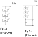
- a first ESD protecting circuit 110a includes a plurality of OTS devices 111, 112, and 113 connected between the power voltage line VDD and the node A in series.
- the first ESD protecting circuit 110b includes the OTS devices 111, 112, and 113, a resistor R1, and an NMOS transistor N1.
- the OTS devices 111, 112 and 113 are connected between the power voltage line VDD and the resistor R1.
- the resistor R1 is connected between an output node B of the OTS devices 111, 112, and 113 and the node A.
- the node A is connected to the data pad I/O.
- the NMOS transistor N1 connects the power voltage line VDD to the node A in response to a voltage from the output node B of the OTS devices 111, 112, and 113.
- BJT bipolar junction transistor
- a semiconductor device comprises a device with high clamping voltage (HVC device), and an OTS device.
- HVC device high clamping voltage
- OTS device OTS
- the HVC device and the OTS device can be connected in series.
- the HVC device and the OTS device can be combined in a package.
- the OTS device can be integrated in a metal stack of the HVC device.
- a semiconductor device further comprises a first external pin and a second external pin.
- a semiconductor device comprises a HVC device and OTS device.
- the HVC device comprises a p-n-junction with a high breakdown voltage, a first metallization layer and a second metallization layer.
- the OTS device is positioned between the first metallization layer and the second metallization layer of the HVC device. In this way the OTS device is integrated within the HVC device.
- the semiconductor device further comprises a first external pin and a second external pin.
- a semiconductor device comprises a HVC device and OTS device.
- the HVC device comprises two p-n-junctions, wherein a first p-n junction is realized by a first p layer and a n layer, and wherein a second p-n junction is realized by a second p layer and the n layer.
- the HVC device further comprises a first metallization layer, a second metallization layer, a third metallization layer and a fourth metallization layer.
- the OTS device comprises a first OTS layer and a second OTS layer.
- the first metallization layer is positioned on the top of the first p layer, the first OTS layer is positioned on the top of the first metallization layer, and the second metallization layer is positioned on the top of the first OTS layer, so that the first OTS layer is sandwiched between the first metallization layer and the second metallization layer.
- the third metallization layer is positioned on the top of the second p layer, the second OTS layer is positioned on the top of the third metallization layer, and the fourth metallization layer is positioned on the top of the second OTS layer, so that the second OTS layer is sandwiched between the third metallization layer and the fourth metallization layer.
- the semiconductor device further comprises a first external pin and a second external pin.
- a semiconductor device comprises a HVC device and an OTS device.
- the HVC device comprises a p-n-junction with a high breakdown voltage.
- the HVC device further comprises a first metallization layer and a second metallization layer.
- the OTS device is positioned between the first metallization layer and the second metallization layer of the HVC device.
- the OTS device comprises multiple OTS layers that are positioned between the first metallization layer and the second metallization layer of the HVC device.
- the HVC device further comprises a first external pin and a second external pin.
- a HVC device comprises two p-n-junctions, a first p-n junction and a second p-n junction.
- the first p-n junction is realized by a first layer of a first polarity and a second layer of a second polarity.
- the second p-n junction is realized by the second layer and a third layer of the first polarity.
- the OTS device as described in the previous embodiments is preferably tuned so that the robustness of the OTS device mirrors the robustness of the HVC device. This mirroring of the robustness secures achieving a lowest capacitance per robustness ratio for the semiconductor device comprising said HVC device and OTS device.
- the high voltage clamp within the HVC device can be also realized by a BJT device, a MOS device or any other applicable semiconductor structure with a sufficiently high clamping voltage.
- the high voltage clamp of the HVC device has preferably a symmetrical electrical characteristic. In this way the series connection of an OTS device and a HVC device is symmetrical too.
- the semiconductor device as described in the above embodiments provides an advantageous ESD protection wherein the semiconductor device has both, a low capacitance and a high breakdown voltage.
- the present invention also related to a method of producing a semiconductor device as described in the above embodiments.
- a semiconductor device with an ESD protection comprises an OTS device and a device with high clamping voltage.
- Such a semiconductor device solves the problems that are present in the known semiconductor devices.
- the known semiconductor devices with a high clamping voltage have to be relatively big, since there is a large amount of power to be dissipated. Accordingly these devices that are relatively big, have a high capacitance. This makes them unsuitable for high speed data lines.
- OTS devices that are known to be used as a part of onchip ESD protection structures. These OTS devices can offer a relatively low capacitance, low trigger and low holding voltages.
- the semiconductor device according to an embodiment of the present invention does not have the above mentioned problems known in the prior art.
- the OTS device has a low capacitance which compensates for the high capacitance of the device with high clamping voltage.
- the device with high clamping voltage has a high clamping voltage, which adds to a relatively small clamping voltage of the OTS device.
- the semiconductor device according to the embodiment of the present invention which is a combination the OTS device and the device with high clamping voltage, is a semiconductor device with both a relatively small capacitance and a relatively high clamping voltage.
- a semiconductor device according to an embodiment of the present invention is shown in Figure 2a .
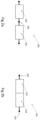
- the semiconductor device 200 comprises an OTS device 202 and a device with high clamping voltage 204 connected in series.
- the device with high clamping voltage 204 is also called a high voltage clamp (HVC) device.
- HVC high voltage clamp
- connection 206 between the OTC device and the HVC device can be realized by a bond-wire, a leadframe, or similar.
- a semiconductor device is shown in Figure 2b .
- the semiconductor device 220 comprises an OTS device 222 and a HVC device 224 combined within one package.
- a package can have two external pins, a first external pin 226 and a second external pin 228.
- the first external pin 226 is connected to the left side of the OTS device 222 and the second external pin 228 is connected to the right side of the HVC device 224.
- the OTS device can be integrated in a metal stack of the HVC device.
- a semiconductor device comprises an OTS device and a HVC device, wherein the OTS device is positioned between two interconnect layers of the HVC device.
- FIG. 3a Three exemplary embodiments of the present invention are shown in Figures 3a, 3b and 3c .
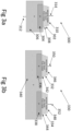
- a semiconductor device 300 comprises:
- the HVC device further comprises a first external pin 312 and a second external pin 314.
- the semiconductor device can comprise more than two metallization layers, and the OTS device can be position between two of any of these multiple metallization layers, e.g. between the third and the fourth metallization layers in case that there are four metallization layers.
- the present invention also includes all polarization combinations, e.g. the junction can be also a n-p-junction, etc. The junction can be positioned deep in the silicon, it comprise a stack of junctions, etc.
- a semiconductor device 330 comprises:
- a HVC device can further comprise two p-n-junctions, a first p-n junction and a second p-n junction.
- the first p-n junction is realized by a first layer of a first polarity and a second layer of a second polarity.
- the second p-n junction is realized by the second layer and a third layer of the first polarity.
- a HVC device comprises two p-n-junctions 336, 338, 340, wherein a first p-n junction is realized by a first p layer 336 and a n layer 340, and wherein a second p-n junction is realized by a second p layer 338 and the n layer 340.
- the semiconductor device can further comprise a first external pin 350 and a second external pin 352.
- This exemplary embodiment shown in Figure 3b is an anti-serial connection of two semiconductor devices shown in Figure 2b .
- a semiconductor device 360 comprises:
- the HVC device further comprises a first external pin 372 and a second external pin 374.
- the sandwiching of the OTS device between two metal layers of the HVC device may be a full area or locally only.
- the OTS area of the OTS device would preferably be tuned so that the robustness of the OTS device mirrors the robustness of the HVC device, which secures achieving a lowest capacitance per robustness ratio for the semiconductor device comprising said HVC device and OTS device.
- the high voltage clamp within the HVC device might be realized as a p-n-junction, as shown in the exemplary embodiments shown in Figures 3a, 3b and 3c , but it could be also realized by a BJT device, a MOS device or any other semiconductor structure with a sufficiently high clamping voltage and sufficiently high robustness.
- the high voltage clamp has a symmetrical electrical characteristic, because then the series connection of an OTS device and a HVC device is symmetrical too.
- a big advantage of integrating the OTS device into the interconnect layers of the HVC device is that existing clamp concepts and diffusion processes can be re-used with changes only in the back end that does not change the principal clamp behaviour.
- the semiconductor devices as described in the previous embodiments provide very advantageous ESD protection.
Landscapes
- Semiconductor Integrated Circuits (AREA)
- Emergency Protection Circuit Devices (AREA)
Abstract
Description
- The present invention relates to a semiconductor device. The invention also relates to a method of manufacturing a semiconductor device.
- A semiconductor device known in the art is shown in
Figures 1a ,1b and 1c . - In
Figure 1a a semiconductor integrated circuit device is illustrated, wherein the semiconductor integrated circuit device has an electrostatic discharge (ESD) protection circuit. - The semiconductor
integrated circuit device 100 includes a data pad I/O, a firstESD protecting circuit 110, a secondESD protecting circuit 120, and aninternal circuit 200. - The data pad I/O is an interface that is used to input data from an external device to the
internal circuit 200 and/or output data from theinternal circuit 200 to the external device. - The first
ESD protecting circuit 110 and the secondESD protecting circuit 120 are arranged between the data pad I/O and theinternal circuit 200 so to protect theinternal circuit 200 from an ESD surge that may flow through the data pad I/O coupled to terminals of a power voltage and a ground voltage. - The first
ESD protecting circuit 110 is connected between the data pad I/O and a power voltage line VDD connected to a power voltage pad P1. The secondESD protecting circuit 120 is connected between the firstESD protecting circuit 110 and a ground voltage line VSS connected to a ground voltage pad P2. As shown inFigure 1a , a node A may be a connection node that connects the data pad I/O, the firstESD protecting circuit 110, and the secondESD protecting circuit 120 to each other. - The first
ESD protecting circuit 110 includes at a resistance changeable device. The resistance changeable device is an ovonic threshold switch (OTS) device. As shown inFigure 1b , a firstESD protecting circuit 110a includes a plurality ofOTS devices - As shown in
Figure 1c , the firstESD protecting circuit 110b includes theOTS devices OTS devices OTS devices OTS devices - It is also known in the prior art to use semiconductor structures only, thus no use of ovonic switching.
- An example of this kind of prior art is a well-known combination of forward diodes in series with a high clamping device.
- It is also known in the prior art to use a bipolar junction transistor (BJT) in a two pin configuration, where the emitter base diode provides the small capacitance, and the base collector junction gives the high clamping voltage. The disadvantage of the semiconductor devices as described above is that it has a non-symmetrical behaviour. To make the system symmetrical, more structures have to be added.
- Various example embodiments are directed to the disadvantage as described above and/or others which may become apparent from the following disclosure.
- According to an embodiment of the present invention a semiconductor device comprises a device with high clamping voltage (HVC device), and an OTS device.
- The HVC device and the OTS device can be connected in series.
- The HVC device and the OTS device can be combined in a package. The OTS device can be integrated in a metal stack of the HVC device.
- According to an embodiment of the present invention a semiconductor device further comprises a first external pin and a second external pin.
- According to an embodiment of the present invention a semiconductor device comprises a HVC device and OTS device. The HVC device comprises a p-n-junction with a high breakdown voltage, a first metallization layer and a second metallization layer. The OTS device is positioned between the first metallization layer and the second metallization layer of the HVC device. In this way the OTS device is integrated within the HVC device. The semiconductor device further comprises a first external pin and a second external pin.
- According to an embodiment of the present invention a semiconductor device comprises a HVC device and OTS device. The HVC device comprises two p-n-junctions, wherein a first p-n junction is realized by a first p layer and a n layer, and wherein a second p-n junction is realized by a second p layer and the n layer. The HVC device further comprises a first metallization layer, a second metallization layer, a third metallization layer and a fourth metallization layer. The OTS device comprises a first OTS layer and a second OTS layer. The first metallization layer is positioned on the top of the first p layer, the first OTS layer is positioned on the top of the first metallization layer, and the second metallization layer is positioned on the top of the first OTS layer, so that the first OTS layer is sandwiched between the first metallization layer and the second metallization layer. The third metallization layer is positioned on the top of the second p layer, the second OTS layer is positioned on the top of the third metallization layer, and the fourth metallization layer is positioned on the top of the second OTS layer, so that the second OTS layer is sandwiched between the third metallization layer and the fourth metallization layer. The semiconductor device further comprises a first external pin and a second external pin.
- According to an embodiment of the present invention a semiconductor device comprises a HVC device and an OTS device. The HVC device comprises a p-n-junction with a high breakdown voltage. The HVC device further comprises a first metallization layer and a second metallization layer. The OTS device is positioned between the first metallization layer and the second metallization layer of the HVC device. The OTS device comprises multiple OTS layers that are positioned between the first metallization layer and the second metallization layer of the HVC device. The HVC device further comprises a first external pin and a second external pin.
- According to an embodiment of the present invention a HVC device comprises two p-n-junctions, a first p-n junction and a second p-n junction. The first p-n junction is realized by a first layer of a first polarity and a second layer of a second polarity. The second p-n junction is realized by the second layer and a third layer of the first polarity.
- The OTS device as described in the previous embodiments is preferably tuned so that the robustness of the OTS device mirrors the robustness of the HVC device. This mirroring of the robustness secures achieving a lowest capacitance per robustness ratio for the semiconductor device comprising said HVC device and OTS device.
- The high voltage clamp within the HVC device can be also realized by a BJT device, a MOS device or any other applicable semiconductor structure with a sufficiently high clamping voltage.
- The high voltage clamp of the HVC device has preferably a symmetrical electrical characteristic. In this way the series connection of an OTS device and a HVC device is symmetrical too.
- The semiconductor device as described in the above embodiments provides an advantageous ESD protection wherein the semiconductor device has both, a low capacitance and a high breakdown voltage.
- The present invention also related to a method of producing a semiconductor device as described in the above embodiments.
- So that the manner in which the features of the present disclosure can be understood in detail, a more particular description is made with reference to embodiments, some of which are illustrated in the appended figures. It is to be noted, however, that the appended figures illustrate only typical embodiments and are therefore not to be considered limiting of its scope. The figures are for facilitating an understanding of the disclosure and thus are not necessarily drawn to scale. Advantages of the subject matter claimed will become apparent to those skilled in the art upon reading this description in conjunction with the accompanying figures, in which like reference numerals have been used to designate like elements, and in which:
-
Figures 1a ,1b and 1c show a known semiconductor device; -
Figures 2a and 2b illustrate semiconductor devices according to embodiments of the present invention; -
Figures 3a, 3b and 2c illustrate semiconductor devices according to embodiments of the present invention. - According to an embodiment of the present invention, a semiconductor device with an ESD protection is provided, which semiconductor device comprises an OTS device and a device with high clamping voltage.
- Such a semiconductor device solves the problems that are present in the known semiconductor devices. The known semiconductor devices with a high clamping voltage have to be relatively big, since there is a large amount of power to be dissipated. Accordingly these devices that are relatively big, have a high capacitance. This makes them unsuitable for high speed data lines.
- Known ESD protection devices with a relatively small capacitance have a small holding voltage, making them unsuitable for the high voltage applications.
- This is also true for the known OTS devices that are known to be used as a part of onchip ESD protection structures. These OTS devices can offer a relatively low capacitance, low trigger and low holding voltages.
- The semiconductor device according to an embodiment of the present invention, the semiconductor device comprising an OTS device and a device with high clamping voltage, does not have the above mentioned problems known in the prior art.
- The OTS device has a low capacitance which compensates for the high capacitance of the device with high clamping voltage.
- The device with high clamping voltage has a high clamping voltage, which adds to a relatively small clamping voltage of the OTS device.
- Therefore, the semiconductor device according to the embodiment of the present invention, which is a combination the OTS device and the device with high clamping voltage, is a semiconductor device with both a relatively small capacitance and a relatively high clamping voltage.
- According to an embodiment of the invention a semiconductor device which is a combination of an OTS device and a device with high clamping voltage may be realized in at least two ways:
- an OTS device and a device with high clamping voltage can be realized as discrete, independent devices that are combined in one semiconductor package, or
- an OTS device can be integrated into interconnect layers of a device with high clamping voltage by integration.
- A semiconductor device according to an embodiment of the present invention is shown in
Figure 2a . Thesemiconductor device 200 comprises anOTS device 202 and a device withhigh clamping voltage 204 connected in series. The device withhigh clamping voltage 204 is also called a high voltage clamp (HVC) device. - The
connection 206 between the OTC device and the HVC device can be realized by a bond-wire, a leadframe, or similar. - A semiconductor device according to an embodiment of the present invention is shown in
Figure 2b . Thesemiconductor device 220 comprises anOTS device 222 and aHVC device 224 combined within one package. Such a package can have two external pins, a firstexternal pin 226 and a secondexternal pin 228. In this exemplary embodiment shown inFigure 2b , the firstexternal pin 226 is connected to the left side of theOTS device 222 and the secondexternal pin 228 is connected to the right side of theHVC device 224. In this case the OTS device can be integrated in a metal stack of the HVC device. - In an embodiment of the present invention a semiconductor device comprises an OTS device and a HVC device, wherein the OTS device is positioned between two interconnect layers of the HVC device.
- Three exemplary embodiments of the present invention are shown in
Figures 3a, 3b and3c . - In an exemplary embodiment of the present invention shown in
Figure 3a , asemiconductor device 300 comprises: - a HVC device, which HVC device comprises a p-n-
junction first metallization layer 308 and asecond metallization layer 310, and - an
OTS device 302 which is positioned between thefirst metallization layer 308 and thesecond metallization layer 310 of the HVC device. - The HVC device further comprises a first
external pin 312 and a secondexternal pin 314. - The present invention includes all variation of the above described embodiment. For example, the semiconductor device can comprise more than two metallization layers, and the OTS device can be position between two of any of these multiple metallization layers, e.g. between the third and the fourth metallization layers in case that there are four metallization layers. Moreover, the present invention also includes all polarization combinations, e.g. the junction can be also a n-p-junction, etc. The junction can be positioned deep in the silicon, it comprise a stack of junctions, etc.
- In an exemplary embodiment of the present invention shown in
Figure 3b , asemiconductor device 330 comprises: - a HVC device, which HVC device comprises a
first metallization layer 342, asecond metallization layer 346, athird metallization layer 344 and afourth metallization layer 348, and - an
OTS device first OTS layer 332 and asecond OTS layer 334, - wherein the
first metallization layer 342 is positioned on the top of thefirst p layer 336, thefirst OTS layer 332 is positioned on the top of thefirst metallization layer 342, and thesecond metallization layer 346 is positioned on the top of thefirst OTS layer 332, so that thefirst OTS layer 332 is sandwiched between thefirst metallization layer 342 and thesecond metallization layer 346, and - wherein the
third metallization layer 344 is positioned on the top of thesecond p layer 338, thesecond OTS layer 334 is positioned on the top of thethird metallization layer 344, and thefourth metallization layer 348 is positioned on the top of thesecond OTS layer 334, so that thesecond OTS layer 334 is sandwiched between thethird metallization layer 344 and thefourth metallization layer 348. - According to an embodiment of the present invention a HVC device can further comprise two p-n-junctions, a first p-n junction and a second p-n junction. The first p-n junction is realized by a first layer of a first polarity and a second layer of a second polarity. The second p-n junction is realized by the second layer and a third layer of the first polarity.
- In exemplary embodiment shown in
Figure 3b , a HVC device comprises two p-n-junctions first p layer 336 and a nlayer 340, and wherein a second p-n junction is realized by asecond p layer 338 and then layer 340. - The semiconductor device can further comprise a first
external pin 350 and a secondexternal pin 352. - This exemplary embodiment shown in
Figure 3b is an anti-serial connection of two semiconductor devices shown inFigure 2b . - In an exemplary embodiment of the present invention shown in
Figure 3c , asemiconductor device 360 comprises: - a HVC device, which HVC device comprises a p-n-
junction first metallization layer 368 and asecond metallization layer 370, and - an
OTS device 362 which is positioned between thefirst metallization layer 368 and thesecond metallization layer 370 of the HVC device, wherein theOTS device 362 comprisesmultiple OTS layers 362 that are positioned between thefirst metallization layer 368 and thesecond metallization layer 370 of the HVC device. - The HVC device further comprises a first
external pin 372 and a secondexternal pin 374. - As shown in the previous embodiments of the present invention, the sandwiching of the OTS device between two metal layers of the HVC device may be a full area or locally only.
- The OTS area of the OTS device would preferably be tuned so that the robustness of the OTS device mirrors the robustness of the HVC device, which secures achieving a lowest capacitance per robustness ratio for the semiconductor device comprising said HVC device and OTS device.
- The high voltage clamp within the HVC device might be realized as a p-n-junction, as shown in the exemplary embodiments shown in
Figures 3a, 3b and3c , but it could be also realized by a BJT device, a MOS device or any other semiconductor structure with a sufficiently high clamping voltage and sufficiently high robustness. - Preferably the high voltage clamp has a symmetrical electrical characteristic, because then the series connection of an OTS device and a HVC device is symmetrical too.
- A big advantage of integrating the OTS device into the interconnect layers of the HVC device is that existing clamp concepts and diffusion processes can be re-used with changes only in the back end that does not change the principal clamp behaviour.
- The semiconductor devices as described in the previous embodiments provide very advantageous ESD protection.
- Particular and preferred aspects of the invention are set out in the accompanying independent claims. Combinations of features from the dependent and/or independent claims may be combined as appropriate and not merely as set out in the claims.
- The scope of the present disclosure includes any novel feature or combination of features disclosed therein either explicitly or implicitly or any generalisation thereof irrespective of whether or not it relates to the claimed invention or mitigate against any or all of the problems addressed by the present invention. The applicant hereby gives notice that new claims may be formulated to such features during prosecution of this application or of any such further application derived therefrom. In particular, with reference to the appended claims, features from dependent claims may be combined with those of the independent claims and features from respective independent claims may be combined in any appropriate manner and not merely in specific combinations enumerated in the claims.
- Features which are described in the context of separate embodiments may also be provided in combination in a single embodiment. Conversely, various features which are, for brevity, described in the context of a single embodiment, may also be provided separately or in any suitable sub combination.
- Term "comprising" does not exclude other elements or steps, the term "a" or "an" does not exclude a plurality. Reference signs in the claims shall not be construed as limiting the scope of the claims.
Claims (12)
- A semiconductor device comprising:- a device with high clamping voltage (HVC device), and- an OTS device.
- A semiconductor device as claimed in claim 1, wherein the HVC device and the OTS device are connected in series.
- A semiconductor device as claimed in any of the previous claims, wherein the HVC device and the OTS device are combined in a package.
- A semiconductor device as claimed in any of the previous claims, wherein the OTS device is integrated in a metal stack of the HVC device.
- A semiconductor device as claimed in any of the previous claims, wherein the semiconductor device further comprises a first external pin and a second external pin.
- A semiconductor device as claimed in any of the previous claims,- wherein the HVC device comprises:∘ at least one p-n-junction with a high breakdown voltage,∘ a first metallization layer, and∘ a second metallization layer,- wherein the OTS device is positioned between the first metallization layer and the second metallization layer the HVC device.
- A semiconductor device as claimed in any of the previous claims,- wherein the HVC device comprises:
∘ a first metallization layer, a second metallization layer, a third metallization layer and a fourth metallization layer,- wherein the OTS device comprises a first OTS layer and a second OTS layer,- wherein the first metallization layer is positioned on the top of the first p layer, the first OTS layer is positioned on the top of the first metallization layer, and the second metallization layer is positioned on the top of the first OTS layer, so that the first OTS layer is sandwiched between the first metallization layer and the second metallization layer,- wherein the third metallization layer is positioned on the top of the second p layer, the second OTS layer is positioned on the top of the third metallization layer, and the fourth metallization layer is positioned on the top of the second OTS layer, so that the second OTS layer is sandwiched between the third metallization layer and the fourth metallization layer. - A semiconductor device as claimed in any of the previous claims,- wherein the HVC device comprises:
∘ two p-n-junctions, a first p-n junction and a second p-n junction, wherein the first p-n junction is realized by a first layer of a first polarity and a second layer of a second polarity, and wherein the second p-n junction is realized by the second layer and a third layer of the first polarity. - A semiconductor device as claimed in any of the previous claims, wherein the OTS device is tuned so that the robustness of the OTS device mirrors the robustness of the HVC device.
- A semiconductor device as claimed in any of the previous claims, wherein the high voltage clamp within the HVC device is realized by a BJT device, a MOS device or any other applicable semiconductor structure with a sufficiently high clamping voltage.
- A semiconductor device as claimed in any of the previous claims, wherein the high voltage clamp of the HVC device has a symmetrical electrical characteristic.
- A method of producing a semiconductor device as claimed in any of the previous claims.
Priority Applications (3)
| Application Number | Priority Date | Filing Date | Title |
|---|---|---|---|
| EP21218429.5A EP4207282A1 (en) | 2021-12-31 | 2021-12-31 | A semiconductor device and a method of manufacturing a semiconductor device |
| US18/147,735 US20230223396A1 (en) | 2021-12-31 | 2022-12-29 | Semiconductor device and a method of manufacturing a semiconductor device |
| CN202211708418.9A CN116387305A (en) | 2021-12-31 | 2022-12-29 | Semiconductor device and method of manufacturing the same |
Applications Claiming Priority (1)
| Application Number | Priority Date | Filing Date | Title |
|---|---|---|---|
| EP21218429.5A EP4207282A1 (en) | 2021-12-31 | 2021-12-31 | A semiconductor device and a method of manufacturing a semiconductor device |
Publications (1)
| Publication Number | Publication Date |
|---|---|
| EP4207282A1 true EP4207282A1 (en) | 2023-07-05 |
Family
ID=79230711
Family Applications (1)
| Application Number | Title | Priority Date | Filing Date |
|---|---|---|---|
| EP21218429.5A Pending EP4207282A1 (en) | 2021-12-31 | 2021-12-31 | A semiconductor device and a method of manufacturing a semiconductor device |
Country Status (3)
| Country | Link |
|---|---|
| US (1) | US20230223396A1 (en) |
| EP (1) | EP4207282A1 (en) |
| CN (1) | CN116387305A (en) |
Citations (6)
| Publication number | Priority date | Publication date | Assignee | Title |
|---|---|---|---|---|
| KR20070038650A (en) * | 2005-10-06 | 2007-04-11 | 삼성전자주식회사 | ESD protection circuit using OST |
| US8350355B2 (en) * | 2010-03-01 | 2013-01-08 | Infineon Technologies Ag | Electrostatic discharge devices |
| US20130163128A1 (en) * | 2011-12-08 | 2013-06-27 | Sofics Bvba | High holding voltage, mixed-voltage domain electrostatic discharge clamp |
| US10388561B2 (en) * | 2016-07-19 | 2019-08-20 | SK Hynix Inc. | Semiconductor integrated circuit device having electrostatic discharge protection circuit |
| US10388646B1 (en) * | 2018-06-04 | 2019-08-20 | Sandisk Technologies Llc | Electrostatic discharge protection devices including a field-induced switching element |
| US20200227914A1 (en) * | 2019-01-10 | 2020-07-16 | Analog Devices International Unlimited Company | Electrical overstress protection with low leakage current for high voltage tolerant high speed interfaces |
-
2021
- 2021-12-31 EP EP21218429.5A patent/EP4207282A1/en active Pending
-
2022
- 2022-12-29 CN CN202211708418.9A patent/CN116387305A/en active Pending
- 2022-12-29 US US18/147,735 patent/US20230223396A1/en active Pending
Patent Citations (6)
| Publication number | Priority date | Publication date | Assignee | Title |
|---|---|---|---|---|
| KR20070038650A (en) * | 2005-10-06 | 2007-04-11 | 삼성전자주식회사 | ESD protection circuit using OST |
| US8350355B2 (en) * | 2010-03-01 | 2013-01-08 | Infineon Technologies Ag | Electrostatic discharge devices |
| US20130163128A1 (en) * | 2011-12-08 | 2013-06-27 | Sofics Bvba | High holding voltage, mixed-voltage domain electrostatic discharge clamp |
| US10388561B2 (en) * | 2016-07-19 | 2019-08-20 | SK Hynix Inc. | Semiconductor integrated circuit device having electrostatic discharge protection circuit |
| US10388646B1 (en) * | 2018-06-04 | 2019-08-20 | Sandisk Technologies Llc | Electrostatic discharge protection devices including a field-induced switching element |
| US20200227914A1 (en) * | 2019-01-10 | 2020-07-16 | Analog Devices International Unlimited Company | Electrical overstress protection with low leakage current for high voltage tolerant high speed interfaces |
Also Published As
| Publication number | Publication date |
|---|---|
| CN116387305A (en) | 2023-07-04 |
| US20230223396A1 (en) | 2023-07-13 |
Similar Documents
| Publication | Publication Date | Title |
|---|---|---|
| US6512662B1 (en) | Single structure all-direction ESD protection for integrated circuits | |
| KR100751104B1 (en) | Bidirectional Devices and Diodes and Protection Circuit Devices | |
| JP3226152B2 (en) | Multi-chip semiconductor structure for preventing electrostatic discharge between chips and manufacturing method thereof | |
| US6400542B1 (en) | ESD protection circuit for different power supplies | |
| US8829570B2 (en) | Switching device for heterojunction integrated circuits and methods of forming the same | |
| US20090026493A1 (en) | Electrostatic Protection Circuit | |
| KR100678781B1 (en) | Circuit protection device, two-terminal device and protected circuit device | |
| KR19980068159A (en) | Electrostatic discharge protection circuit and integrated circuit having it | |
| JP3492666B2 (en) | ESD protection circuit for semiconductor device | |
| US7471493B1 (en) | Fast and compact SCR ESD protection device for high-speed pins | |
| US20240088651A1 (en) | Failsafe Input/Output Electrostatic Discharge Protection With Diodes | |
| US6385116B2 (en) | Semiconductor integrated device | |
| CN101443908A (en) | Body-biased PMOS protection against electrostatic discharge | |
| JP2822915B2 (en) | Semiconductor device | |
| US6891206B2 (en) | Lateral thyristor structure for protection against electrostatic discharge | |
| JPH0282533A (en) | bipolar transistor | |
| Hsu et al. | Optimization on bi-directional PNP ESD protection device for high-voltage FlexRay applications | |
| US20230223396A1 (en) | Semiconductor device and a method of manufacturing a semiconductor device | |
| JP2791067B2 (en) | Monolithic overvoltage protection assembly | |
| EP4213209B1 (en) | Esd protection device | |
| CN113380786B (en) | Structure of thyristor transient voltage suppression protection device with integrated reverse conduction diode | |
| CN113658946B (en) | Multi-channel transient voltage suppression device | |
| KR100885375B1 (en) | Semiconductor Device Including Antistatic Circuit | |
| US7193251B1 (en) | ESD protection cluster and method of providing multi-port ESD protection | |
| TW463442B (en) | Electrostatic discharge protection circuit having common discharge line |
Legal Events
| Date | Code | Title | Description |
|---|---|---|---|
| PUAI | Public reference made under article 153(3) epc to a published international application that has entered the european phase |
Free format text: ORIGINAL CODE: 0009012 |
|
| STAA | Information on the status of an ep patent application or granted ep patent |
Free format text: STATUS: THE APPLICATION HAS BEEN PUBLISHED |
|
| AK | Designated contracting states |
Kind code of ref document: A1 Designated state(s): AL AT BE BG CH CY CZ DE DK EE ES FI FR GB GR HR HU IE IS IT LI LT LU LV MC MK MT NL NO PL PT RO RS SE SI SK SM TR |
|
| STAA | Information on the status of an ep patent application or granted ep patent |
Free format text: STATUS: REQUEST FOR EXAMINATION WAS MADE |
|
| 17P | Request for examination filed |
Effective date: 20240105 |
|
| RBV | Designated contracting states (corrected) |
Designated state(s): AL AT BE BG CH CY CZ DE DK EE ES FI FR GB GR HR HU IE IS IT LI LT LU LV MC MK MT NL NO PL PT RO RS SE SI SK SM TR |
|
| STAA | Information on the status of an ep patent application or granted ep patent |
Free format text: STATUS: EXAMINATION IS IN PROGRESS |
|
| 17Q | First examination report despatched |
Effective date: 20250724 |