EP4203281A1 - Dual output dc-dc boost converter with reduced output leakage - Google Patents
Dual output dc-dc boost converter with reduced output leakage Download PDFInfo
- Publication number
- EP4203281A1 EP4203281A1 EP22211223.7A EP22211223A EP4203281A1 EP 4203281 A1 EP4203281 A1 EP 4203281A1 EP 22211223 A EP22211223 A EP 22211223A EP 4203281 A1 EP4203281 A1 EP 4203281A1
- Authority
- EP
- European Patent Office
- Prior art keywords
- coupled
- switch
- node
- operating phase
- path
- Prior art date
- Legal status (The legal status is an assumption and is not a legal conclusion. Google has not performed a legal analysis and makes no representation as to the accuracy of the status listed.)
- Granted
Links
Images


Classifications
-
- H—ELECTRICITY
- H02—GENERATION; CONVERSION OR DISTRIBUTION OF ELECTRIC POWER
- H02M—APPARATUS FOR CONVERSION BETWEEN AC AND AC, BETWEEN AC AND DC, OR BETWEEN DC AND DC, AND FOR USE WITH MAINS OR SIMILAR POWER SUPPLY SYSTEMS; CONVERSION OF DC OR AC INPUT POWER INTO SURGE OUTPUT POWER; CONTROL OR REGULATION THEREOF
- H02M1/00—Details of apparatus for conversion
- H02M1/0067—Converter structures employing plural converter units, other than for parallel operation of the units on a single load
- H02M1/008—Plural converter units for generating at two or more independent and non-parallel outputs, e.g. systems with plural point of load switching regulators
-
- H—ELECTRICITY
- H02—GENERATION; CONVERSION OR DISTRIBUTION OF ELECTRIC POWER
- H02M—APPARATUS FOR CONVERSION BETWEEN AC AND AC, BETWEEN AC AND DC, OR BETWEEN DC AND DC, AND FOR USE WITH MAINS OR SIMILAR POWER SUPPLY SYSTEMS; CONVERSION OF DC OR AC INPUT POWER INTO SURGE OUTPUT POWER; CONTROL OR REGULATION THEREOF
- H02M1/00—Details of apparatus for conversion
- H02M1/0083—Converters characterised by their input or output configuration
- H02M1/009—Converters characterised by their input or output configuration having two or more independently controlled outputs
-
- H—ELECTRICITY
- H02—GENERATION; CONVERSION OR DISTRIBUTION OF ELECTRIC POWER
- H02M—APPARATUS FOR CONVERSION BETWEEN AC AND AC, BETWEEN AC AND DC, OR BETWEEN DC AND DC, AND FOR USE WITH MAINS OR SIMILAR POWER SUPPLY SYSTEMS; CONVERSION OF DC OR AC INPUT POWER INTO SURGE OUTPUT POWER; CONTROL OR REGULATION THEREOF
- H02M1/00—Details of apparatus for conversion
- H02M1/0003—Details of control, feedback or regulation circuits
- H02M1/0038—Circuits or arrangements for suppressing, e.g. by masking incorrect turn-on or turn-off signals, e.g. due to current spikes in current mode control
-
- H—ELECTRICITY
- H02—GENERATION; CONVERSION OR DISTRIBUTION OF ELECTRIC POWER
- H02M—APPARATUS FOR CONVERSION BETWEEN AC AND AC, BETWEEN AC AND DC, OR BETWEEN DC AND DC, AND FOR USE WITH MAINS OR SIMILAR POWER SUPPLY SYSTEMS; CONVERSION OF DC OR AC INPUT POWER INTO SURGE OUTPUT POWER; CONTROL OR REGULATION THEREOF
- H02M1/00—Details of apparatus for conversion
- H02M1/32—Means for protecting converters other than automatic disconnection
-
- H—ELECTRICITY
- H02—GENERATION; CONVERSION OR DISTRIBUTION OF ELECTRIC POWER
- H02M—APPARATUS FOR CONVERSION BETWEEN AC AND AC, BETWEEN AC AND DC, OR BETWEEN DC AND DC, AND FOR USE WITH MAINS OR SIMILAR POWER SUPPLY SYSTEMS; CONVERSION OF DC OR AC INPUT POWER INTO SURGE OUTPUT POWER; CONTROL OR REGULATION THEREOF
- H02M3/00—Conversion of DC power input into DC power output
- H02M3/02—Conversion of DC power input into DC power output without intermediate conversion into AC
- H02M3/04—Conversion of DC power input into DC power output without intermediate conversion into AC by static converters
- H02M3/10—Conversion of DC power input into DC power output without intermediate conversion into AC by static converters using discharge tubes with control electrode or semiconductor devices with control electrode
- H02M3/145—Conversion of DC power input into DC power output without intermediate conversion into AC by static converters using discharge tubes with control electrode or semiconductor devices with control electrode using devices of a triode or transistor type requiring continuous application of a control signal
- H02M3/155—Conversion of DC power input into DC power output without intermediate conversion into AC by static converters using discharge tubes with control electrode or semiconductor devices with control electrode using devices of a triode or transistor type requiring continuous application of a control signal using semiconductor devices only
- H02M3/156—Conversion of DC power input into DC power output without intermediate conversion into AC by static converters using discharge tubes with control electrode or semiconductor devices with control electrode using devices of a triode or transistor type requiring continuous application of a control signal using semiconductor devices only with automatic control of output voltage or current, e.g. switching regulators
-
- H—ELECTRICITY
- H02—GENERATION; CONVERSION OR DISTRIBUTION OF ELECTRIC POWER
- H02M—APPARATUS FOR CONVERSION BETWEEN AC AND AC, BETWEEN AC AND DC, OR BETWEEN DC AND DC, AND FOR USE WITH MAINS OR SIMILAR POWER SUPPLY SYSTEMS; CONVERSION OF DC OR AC INPUT POWER INTO SURGE OUTPUT POWER; CONTROL OR REGULATION THEREOF
- H02M3/00—Conversion of DC power input into DC power output
- H02M3/02—Conversion of DC power input into DC power output without intermediate conversion into AC
- H02M3/04—Conversion of DC power input into DC power output without intermediate conversion into AC by static converters
- H02M3/10—Conversion of DC power input into DC power output without intermediate conversion into AC by static converters using discharge tubes with control electrode or semiconductor devices with control electrode
- H02M3/145—Conversion of DC power input into DC power output without intermediate conversion into AC by static converters using discharge tubes with control electrode or semiconductor devices with control electrode using devices of a triode or transistor type requiring continuous application of a control signal
- H02M3/155—Conversion of DC power input into DC power output without intermediate conversion into AC by static converters using discharge tubes with control electrode or semiconductor devices with control electrode using devices of a triode or transistor type requiring continuous application of a control signal using semiconductor devices only
- H02M3/156—Conversion of DC power input into DC power output without intermediate conversion into AC by static converters using discharge tubes with control electrode or semiconductor devices with control electrode using devices of a triode or transistor type requiring continuous application of a control signal using semiconductor devices only with automatic control of output voltage or current, e.g. switching regulators
- H02M3/158—Conversion of DC power input into DC power output without intermediate conversion into AC by static converters using discharge tubes with control electrode or semiconductor devices with control electrode using devices of a triode or transistor type requiring continuous application of a control signal using semiconductor devices only with automatic control of output voltage or current, e.g. switching regulators including plural semiconductor devices as final control devices for a single load
-
- H—ELECTRICITY
- H02—GENERATION; CONVERSION OR DISTRIBUTION OF ELECTRIC POWER
- H02M—APPARATUS FOR CONVERSION BETWEEN AC AND AC, BETWEEN AC AND DC, OR BETWEEN DC AND DC, AND FOR USE WITH MAINS OR SIMILAR POWER SUPPLY SYSTEMS; CONVERSION OF DC OR AC INPUT POWER INTO SURGE OUTPUT POWER; CONTROL OR REGULATION THEREOF
- H02M1/00—Details of apparatus for conversion
- H02M1/0043—Converters switched with a phase shift, i.e. interleaved
-
- H—ELECTRICITY
- H02—GENERATION; CONVERSION OR DISTRIBUTION OF ELECTRIC POWER
- H02M—APPARATUS FOR CONVERSION BETWEEN AC AND AC, BETWEEN AC AND DC, OR BETWEEN DC AND DC, AND FOR USE WITH MAINS OR SIMILAR POWER SUPPLY SYSTEMS; CONVERSION OF DC OR AC INPUT POWER INTO SURGE OUTPUT POWER; CONTROL OR REGULATION THEREOF
- H02M1/00—Details of apparatus for conversion
- H02M1/32—Means for protecting converters other than automatic disconnection
- H02M1/34—Snubber circuits
- H02M1/342—Active non-dissipative snubbers
-
- Y—GENERAL TAGGING OF NEW TECHNOLOGICAL DEVELOPMENTS; GENERAL TAGGING OF CROSS-SECTIONAL TECHNOLOGIES SPANNING OVER SEVERAL SECTIONS OF THE IPC; TECHNICAL SUBJECTS COVERED BY FORMER USPC CROSS-REFERENCE ART COLLECTIONS [XRACs] AND DIGESTS
- Y02—TECHNOLOGIES OR APPLICATIONS FOR MITIGATION OR ADAPTATION AGAINST CLIMATE CHANGE
- Y02B—CLIMATE CHANGE MITIGATION TECHNOLOGIES RELATED TO BUILDINGS, e.g. HOUSING, HOUSE APPLIANCES OR RELATED END-USER APPLICATIONS
- Y02B70/00—Technologies for an efficient end-user side electric power management and consumption
- Y02B70/10—Technologies improving the efficiency by using switched-mode power supplies [SMPS], i.e. efficient power electronics conversion e.g. power factor correction or reduction of losses in power supplies or efficient standby modes
Definitions
- This disclosure is directed to the field of DC-DC boost converters and, in particular, to a dual output DC-DC boost converter utilizing clamping between output lines so as to reduce output leakage.
- DC-DC boost converters are utilized to step up an input voltage (while stepping down an input current) to produce a high voltage output.
- One of many uses for DC-DC boost converters is in the driving of piezoelectrically actuated micro-electromechanical systems (MEMS) mirror devices.
- MEMS micro-electromechanical systems
- Devices incorporating MEMS mirror devices may utilize two such MEMS mirror devices to scan an incident light beam in a desired two-dimensional scan pattern across a target area.
- a sample known DC-DC boost converter 1 used in a system for driving a pair of MEMS mirror devices is shown in FIG. 1 .
- the DC-DC boost converter 1 receives an input voltage Vin through an input inductor L, the input inductor L being connected to node Nn, at which a voltage SW is produced during operation.
- a first diode D1 is connected between node Nn and a first output capacitor C1 across which a first boosted output voltage VBOOSTL is produced.
- a first switch S1 is connected between node Nn and ground. The first switch S1 is operated by a drive main control signal Drive_Main_SW.
- a second diode D2 is connected between node Nn and a second output capacitor C2 by a switch S2 (e.g., NMOS transistor).
- a second boosted output voltage VBOOSTR (for, for example, may be lower than the first boosted output voltage VBOOSTL) is produced across the second output capacitor C2.
- the NMOS transistor S2 is operated by a drive line control signal Drive_Line_SW.
- the switch control signal Drive_Main_SW is asserted to close switch S1 to thereby connect node Nn to ground.
- the drive line control signal Drive_Line_SW is kept asserted throughout the VBOOSTR phase.
- the switch control signal Drive _Main_SW is asserted to open switch S1
- a boosted voltage SW is produced at node Nn, as can be seen in FIG. 2 .
- current is delivered to charge capacitor C2, increasing the voltage VBOOSTR stored on capacitor C2.
- the DC-DC boost converter includes an inductor coupled between an input voltage and an input node, a first path coupled between the input node and a first output node at which a first output voltage is generated, a second path coupled between the input node and a second output node at which a second output voltage is generated, and a first switch selectively coupling the second path to the first path in response to a first control signal.
- the DC-DC boost converter is configured to: operate in a first operating phase in which the first path boosts the first output voltage and in which the second path is kept from boosting the second output voltage by the first control signal being asserted to cause the first switch to couple the second path to the first path; and operate in a second operating phase in which the second path boosts the second output voltage and in which the first path is kept from boosting the first output voltage.
- the first path may include a first diode having an anode coupled to the input node and a cathode coupled to the first output node, and a first capacitor coupled between the first output node and ground, wherein the first output voltage is generated across the first capacitor.
- the second path may include a second diode having an anode coupled to the input node and a cathode coupled to an intermediate node, a second switch coupled between the intermediate node and the second output node, the second switch being controlled by a second control signal, and a second capacitor coupled between the second output node and ground, wherein the second output voltage is generated across the second capacitor.
- the first switch may selectively couple the intermediate node to the cathode of the first diode in the first operating phase
- the second control signal may be asserted to cause the second switch to selectively couple the intermediate node to the second output node during the second operating phase.
- An additional switch may be coupled between the input node and ground, the additional switch controlled by an additional control signal, with the additional control signal being asserted to close the additional switch during a first portion of the first operating phase and being deasserted to open the additional switch during a second portion of the first operating phase. Also, the additional control signal may be asserted to close the additional switch during a first portion of the second operating phase and is deasserted to open the additional switch during a second portion of the second operating phase.
- the second switch may be an NMOS transistor having a drain coupled to the intermediate node, a source coupled to the second output node, and a gate coupled to receive the second control signal.
- the first switch may be a PMOS transistor having a source coupled to the first output node, a drain coupled to the intermediate node, and a gate coupled to receive the first control signal.
- a first feedback circuit may be coupled to the first output node, the first feedback circuit generating a first feedback voltage.
- a second feedback circuit may be coupled to the second output node, the second feedback circuit generating a second feedback voltage.
- a controller may be configured to generate the first and second control signals based upon the first and second feedback voltages.
- First drive circuitry may be powered by the first output voltage, and a first micromirror may be driven by the first drive circuitry.
- Second drive circuitry may be powered by the second output voltage, and a second micromirror may be driven by the second drive circuitry.
- a DC-DC boost converter including a first diode coupled between an input node and a first output node, wherein a first capacitor is coupled between the first output node and ground such that a first output voltage is generated across the first capacitor.
- the DC-DC boost converter also includes a first switch coupled between the input node and ground, the first switch operated by a first control signal, a second diode coupled between the input node and an intermediate node, a second switch coupled between the intermediate node and a second output node, the second switch operated by a second control signal, wherein a second capacitor is coupled between the output node and ground such that a second output voltage is generated across the second capacitor.
- a third switch is coupled between the intermediate node and the first output node, the third switch operated by a third control signal.
- a controller is configured to generate the first, second, and third control signals so as to: in a first operating phase, close the first switch during a first portion of the first operating phase and open the first switch during a second portion of the first operating phase, open the second switch during the first operating phase, and close the third switch during the first operating phase; and in a second operating phase, close the first switch during a first portion of the second operating phase and open the first switch during a second portion of the second operating phase, close the second switch during the second operating phase, and open the third switch during the second operating phase.
- the second switch may be an NMOS transistor having a drain coupled to the intermediate node, a source coupled to the second output node, and a gate coupled to receive the second control signal.
- the third switch may be a PMOS transistor having a source coupled to the first output node, a drain coupled to the intermediate node, and a gate coupled to receive the third control signal.
- a first feedback circuit may be coupled to the first output node, the first feedback circuit generating a first feedback voltage.
- a second feedback circuit may be coupled to the second output node, the second feedback circuit generating a second feedback voltage.
- the controller may be configured to generate the first, second, and third control signals based upon the first and second feedback voltages.
- a method described herein includes operating a DC-DC boost controller in a first operating phase in which a first path boosts an input voltage to produce a first output voltage and in which a second path is kept from boosting a second output voltage by clamping the second path to the first path, and operating the DC-DC boost controller in a second operating phase in which the second path boosts the second output voltage and in which the first path is kept from boosting the first output voltage, wherein the second path is not clamped to the first path during the second operating phase.
- the method also includes, in the first operating phase, charging an inductor coupled to the input voltage during a first portion of the first operating phase and permitting the inductor to discharge during a second portion of the first operating phase.
- the method also includes, in the second operating phase, charging the inductor during a first portion of the second operating phase and permitting the inductor to discharge during a second portion of the second operating phase.
- any described resistor or resistance is a discrete device unless the contrary is stated, and is not simply an electrical lead between two points. Thus, any described resistor or resistance coupled between two points has a greater resistance than a lead between those two points would have, and such resistor or resistance cannot be interpreted to be a lead.
- any described capacitor or capacitance is a discrete device unless the contrary is stated, and is not a parasitic.
- any described inductor or inductance is a discrete device unless the contrary is stated, and is not a parasitic.
- a driving system 10 for a pair of MEMS mirror devices 14 (e.g., a first MEMS mirror 14a and a second MEMS mirror 14b operated at the same or a different frequency) is shown in FIG. 3 .
- the driving system 10 may be incorporated within a picoprojector, headset, or depth sensing system.
- the driving system 10 includes a DC-DC boost converter 11 receiving an input voltage Vin and boosting that input voltage to produce two output voltages VBOOSTL and VBOOSTR.
- Vin may be on the order of 3.3V
- VBOOSTL may be on the order of 19V to 45V
- VBOOSTR may be on the order of 14V to 40V.
- the voltage VBOOSTL is fed as input to a low dropout (LDO) voltage regulator 12a, which provides output supply voltage to driver circuitry 13a.
- LDO low dropout
- the driver circuitry 13a using a power supply voltage produced by the LDO voltage regulator 12a and under control of a low voltage drive control signal LV_Drive_Signal1, generates a high voltage drive signal HV_Drive_Signal1 used to drive the MEMS mirror 14a (for example, at resonance).
- the voltage VBOOSTR is fed as input to a low dropout (LDO) voltage regulator 12b, which provides output supply voltage to driver circuitry 13b.
- the driver circuitry 13b using a power supply voltage produced by the LDO voltage regulator 12b and under control of a low voltage drive control signal LV_Drive_Signal2, generates a high voltage drive signal HV_Drive_Signal2 used to drive the MEMS mirror 14b (for example, in a linear fashion).
- the DC-DC boost converter 11 receives an input voltage Vin through an input inductor L, the input inductor L being connected to node Nn at which a voltage SW is produced during operation.
- a first diode D1 has its anode connected to node Nn and its cathode connected to a first terminal of a first output capacitor C1 across which a first boosted output voltage VBOOSTL is produced.
- a second terminal of the first output capacitor C1 is connected to ground.
- the first terminal of the first output capacitor C1 is coupled to ground through series connected resistors R1 and R2, with a node N1 being a tap between the resistors R1 and R2.
- a first feedback voltage Fbk1 is produced at node N1.
- a first switch S1 is connected between node Nn and ground.
- the first switch S1 may be a transistor, such an NMOS transistor, and is operated by a drive main control signal Drive_Main_SW.
- a second diode D2 has its anode connected to node Nn and its cathode connected to a drain of a second switch S2 (e.g., an NMOS transistor).
- the NMOS transistor S2 has its source connected to a first terminal of a second output capacitor C2, and has its gate connected to a drive line control signal Drive_Line_SW.
- a second terminal of the second output capacitor C2 is connected to ground.
- a second boosted output voltage VBOOSTR is produced across the second output capacitor C2.
- the first terminal of the second output capacitor C2 is coupled to ground through series connected resistors R3 and R4, with a node N2 being a tap between the resistors R3 and R4.
- a second feedback voltage Fbk2 is produced at node N2.
- a third switch S3 (e.g., a PMOS transistor) has its source connected to the first terminal of the first output capacitor C1, its drain connected to the cathode of the diode D2 and drain of NMOS transistor S2, and its gate connected to Drive Line SW.
- S3 could be an NMOS transistor having its drain connected to the first terminal of the first output capacitor C1, its source connected to the cathode of the diode D2 and the drain of NMOS transistor S2, and its gate connected to Drive_Neg_Line_SW, with Drive_Neg_Line in this instance being a logical invert of Drive_Line_SW.
- a control loop circuit 21 has inputs connected to nodes N1 and N2 to thereby receive the feedback voltages Fbk1 and FBk2 as input.
- the control loop circuit 21 has outputs generating the drive main control signal Drive_Main_SW and the drive line switch control signal Drive_Line_SW.
- the control loop circuit 21 generates its outputs based upon its inputs so as to produce the desired VBOOSTL and VBOOSTR voltages.
- the drive line switch control signal Drive_Line_SW is deasserted during the VBOOSTL phase.
- the NMOS transistor S2 is intended to remain off, while the PMOS transistor S3 is turned on.
- Turning on of the transistor S3 serves to clamp the drain of the NMOS transistor S2 (and therefore the voltage Vline) to VBOOSTL during the VBOOSTL phase, which has the result of preventing the diode D2 from becoming forward biased and prevents the coupling of the voltage SW to the gate of NMOS transistor S2 through the parasitic drain-gate capacitance of S2, keeping NMOS transistor S2 off.
- Drive Main SW is asserted to close switch S1 to thereby connect node Nn to ground, with the result being that the current through the inductor L ramps upwardly as shown, generating a magnetic field and thereby storing energy in the inductor L.
- Drive_Main_SW is deasserted to open switch S1
- the current into the inductor L falls as can be seen, and the strength of the magnetic field collapses as the stored energy is converted to current to attempt to maintain the current output from the inductor L.
- the left side of the inductor L goes positive, meaning that the voltage across the inductor L is in series with the input voltage Vin, thereby providing a boosted voltage SW at the right side of the inductor L (node Nin).
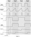
- the rise in this voltage SW during the VBOOSTL phase when the switch S 1 opens can be seen in FIG. 5 .
- the rise in the voltage SW does not cause the diode D1 to become forward biased because VBOOSTL has not yet fallen sufficiently for such condition to occur, and therefore VBOOSTL continues to ramp downward during the VBOOSTR phase.
- the drive line control signal Drive_Line_SW is asserted during the VBOOSTR phase.
- the NMOS transistor S2 is turned on, and current is sourced to capacitor C2, boosting VBOOSTR during the VBOOSTR phase, as can be seen in FIG. 5 . Since the diode D1 does not become forward biased, as stated, VBOOSTL is not boosted during the VBOOSTR phase.
Landscapes
- Engineering & Computer Science (AREA)
- Power Engineering (AREA)
- Dc-Dc Converters (AREA)
- Physics & Mathematics (AREA)
- General Physics & Mathematics (AREA)
- Optics & Photonics (AREA)
Abstract
Description
- This disclosure is directed to the field of DC-DC boost converters and, in particular, to a dual output DC-DC boost converter utilizing clamping between output lines so as to reduce output leakage.
- DC-DC boost converters are utilized to step up an input voltage (while stepping down an input current) to produce a high voltage output. One of many uses for DC-DC boost converters is in the driving of piezoelectrically actuated micro-electromechanical systems (MEMS) mirror devices. Devices incorporating MEMS mirror devices may utilize two such MEMS mirror devices to scan an incident light beam in a desired two-dimensional scan pattern across a target area.
- A sample known DC-
DC boost converter 1 used in a system for driving a pair of MEMS mirror devices (e.g., a pair of MEMS mirror devices working at a same frequency or different frequencies) is shown inFIG. 1 . The DC-DC boost converter 1 receives an input voltage Vin through an input inductor L, the input inductor L being connected to node Nn, at which a voltage SW is produced during operation. A first diode D1 is connected between node Nn and a first output capacitor C1 across which a first boosted output voltage VBOOSTL is produced. A first switch S1 is connected between node Nn and ground. The first switch S1 is operated by a drive main control signal Drive_Main_SW. A second diode D2 is connected between node Nn and a second output capacitor C2 by a switch S2 (e.g., NMOS transistor). A second boosted output voltage VBOOSTR (for, for example, may be lower than the first boosted output voltage VBOOSTL) is produced across the second output capacitor C2. The NMOS transistor S2 is operated by a drive line control signal Drive_Line_SW. - Operation is now described with additional reference to
FIG. 2 , where thecircuit 1 alternates between phases in which the voltage VBOOSTL is boosted and in which the voltage VBOOSTR is boosted. At the start of the VBOOSTL phase, as can be seen inFIG. 2 , the switch control signal Drive_Main_SW is asserted to close switch S1 to thereby connect node Nn to ground. - When the switch control signal Drive_Main_SW is deasserted to open switch S1, a boosted voltage SW is produced at node Nn, as can be seen in
FIG. 2 . As a result, current is delivered to charge capacitor C1, increasing the voltage VBOOSTL stored on capacitor C1. This is the intention during the VBOOSTL phase. - At the start of the VBOOSTR phase, the switch control signal Drive_Main_SW is asserted to close switch S1 to thereby connect node Nn to ground. The drive line control signal Drive_Line_SW is kept asserted throughout the VBOOSTR phase. When the switch control signal Drive _Main_SW is asserted to open switch S1, a boosted voltage SW is produced at node Nn, as can be seen in
FIG. 2 . As a result, current is delivered to charge capacitor C2, increasing the voltage VBOOSTR stored on capacitor C2. - A problem arises that in the VBOOSTL phase, the gate of the NMOS transistor S2 ends up being coupled to the voltage SW through a parasitic capacitance across the junction of diode D2, and through the parasitic drain-gate capacitance in the NMOS transistor S2. As a result, the voltage Vline at the cathode of diode D2 also rises as the voltage SW rises. This increases the voltage as seen by the gate of S2 independent of the drive line control signal Drive_Line_SW, resulting in S2 weakly turning on and current flowing into capacitor C2 to thereby increase the voltage VBOOSTR. This is undesirable, because current flowing into capacitor C2 reduces current flowing into capacitor C1, and the VBOOSTL phase is intended to charge capacitor C1 to boost VBOOSTL.
- A way to address this would be to add a second NMOS transistor in series with S2, since the current through S2 from its parasitic drain-gate capacitance charging will be insufficient to charge the parasitic drain-gate capacitance of the added NMOS transistor. However, this increases complexity of the system, increases the resistance of the path between diode D2 and capacitor C2 during the VBOOSTR phase when the NMOS transistors are turned on, and increases area consumption. Therefore, further development into DC-DC boost converters is needed.
- Disclosed herein is a device comprising a DC-DC boost converter. The DC-DC boost converter includes an inductor coupled between an input voltage and an input node, a first path coupled between the input node and a first output node at which a first output voltage is generated, a second path coupled between the input node and a second output node at which a second output voltage is generated, and a first switch selectively coupling the second path to the first path in response to a first control signal. The DC-DC boost converter is configured to: operate in a first operating phase in which the first path boosts the first output voltage and in which the second path is kept from boosting the second output voltage by the first control signal being asserted to cause the first switch to couple the second path to the first path; and operate in a second operating phase in which the second path boosts the second output voltage and in which the first path is kept from boosting the first output voltage.
- The first path may include a first diode having an anode coupled to the input node and a cathode coupled to the first output node, and a first capacitor coupled between the first output node and ground, wherein the first output voltage is generated across the first capacitor.
- The second path may include a second diode having an anode coupled to the input node and a cathode coupled to an intermediate node, a second switch coupled between the intermediate node and the second output node, the second switch being controlled by a second control signal, and a second capacitor coupled between the second output node and ground, wherein the second output voltage is generated across the second capacitor. The first switch may selectively couple the intermediate node to the cathode of the first diode in the first operating phase, and the second control signal may be asserted to cause the second switch to selectively couple the intermediate node to the second output node during the second operating phase.
- An additional switch may be coupled between the input node and ground, the additional switch controlled by an additional control signal, with the additional control signal being asserted to close the additional switch during a first portion of the first operating phase and being deasserted to open the additional switch during a second portion of the first operating phase. Also, the additional control signal may be asserted to close the additional switch during a first portion of the second operating phase and is deasserted to open the additional switch during a second portion of the second operating phase.
- The second switch may be an NMOS transistor having a drain coupled to the intermediate node, a source coupled to the second output node, and a gate coupled to receive the second control signal.
- The first switch may be a PMOS transistor having a source coupled to the first output node, a drain coupled to the intermediate node, and a gate coupled to receive the first control signal.
- A first feedback circuit may be coupled to the first output node, the first feedback circuit generating a first feedback voltage. A second feedback circuit may be coupled to the second output node, the second feedback circuit generating a second feedback voltage. A controller may be configured to generate the first and second control signals based upon the first and second feedback voltages.
- First drive circuitry may be powered by the first output voltage, and a first micromirror may be driven by the first drive circuitry. Second drive circuitry may be powered by the second output voltage, and a second micromirror may be driven by the second drive circuitry.
- Also disclosed herein is a DC-DC boost converter including a first diode coupled between an input node and a first output node, wherein a first capacitor is coupled between the first output node and ground such that a first output voltage is generated across the first capacitor. The DC-DC boost converter also includes a first switch coupled between the input node and ground, the first switch operated by a first control signal, a second diode coupled between the input node and an intermediate node, a second switch coupled between the intermediate node and a second output node, the second switch operated by a second control signal, wherein a second capacitor is coupled between the output node and ground such that a second output voltage is generated across the second capacitor. A third switch is coupled between the intermediate node and the first output node, the third switch operated by a third control signal. A controller is configured to generate the first, second, and third control signals so as to: in a first operating phase, close the first switch during a first portion of the first operating phase and open the first switch during a second portion of the first operating phase, open the second switch during the first operating phase, and close the third switch during the first operating phase; and in a second operating phase, close the first switch during a first portion of the second operating phase and open the first switch during a second portion of the second operating phase, close the second switch during the second operating phase, and open the third switch during the second operating phase.
- The second switch may be an NMOS transistor having a drain coupled to the intermediate node, a source coupled to the second output node, and a gate coupled to receive the second control signal.
- The third switch may be a PMOS transistor having a source coupled to the first output node, a drain coupled to the intermediate node, and a gate coupled to receive the third control signal.
- A first feedback circuit may be coupled to the first output node, the first feedback circuit generating a first feedback voltage. A second feedback circuit may be coupled to the second output node, the second feedback circuit generating a second feedback voltage. The controller may be configured to generate the first, second, and third control signals based upon the first and second feedback voltages.
- A method described herein includes operating a DC-DC boost controller in a first operating phase in which a first path boosts an input voltage to produce a first output voltage and in which a second path is kept from boosting a second output voltage by clamping the second path to the first path, and operating the DC-DC boost controller in a second operating phase in which the second path boosts the second output voltage and in which the first path is kept from boosting the first output voltage, wherein the second path is not clamped to the first path during the second operating phase.
- The method also includes, in the first operating phase, charging an inductor coupled to the input voltage during a first portion of the first operating phase and permitting the inductor to discharge during a second portion of the first operating phase.
- The method also includes, in the second operating phase, charging the inductor during a first portion of the second operating phase and permitting the inductor to discharge during a second portion of the second operating phase.
-
-
FIG. 1 is a schematic diagram of a prior art DC-DC boost converter. -
FIG. 2 is a graph showing signals of the DC-DC boost converter ofFIG. 1 in operation. -
FIG. 3 a block diagram of a driving system for a pair of MEMS mirror devices, disclosed herein. -
FIG. 4 is a schematic block diagram of the DC-DC boost converter ofFIG. 3 . -
FIG. 5 is a graph showing signals of the DC-DC boost converter ofFIG. 4 in operation. - The following disclosure enables a person skilled in the art to make and use the subject matter disclosed herein. The general principles described herein may be applied to embodiments and applications other than those detailed above without departing from the spirit and scope of this disclosure. This disclosure is not intended to be limited to the embodiments shown, but is to be accorded the widest scope consistent with the principles and features disclosed or suggested herein. Do note that in the below description, any described resistor or resistance is a discrete device unless the contrary is stated, and is not simply an electrical lead between two points. Thus, any described resistor or resistance coupled between two points has a greater resistance than a lead between those two points would have, and such resistor or resistance cannot be interpreted to be a lead. Similarly, any described capacitor or capacitance is a discrete device unless the contrary is stated, and is not a parasitic. Moreover, any described inductor or inductance is a discrete device unless the contrary is stated, and is not a parasitic.
- A driving
system 10 for a pair of MEMS mirror devices 14 (e.g., afirst MEMS mirror 14a and asecond MEMS mirror 14b operated at the same or a different frequency) is shown inFIG. 3 . The drivingsystem 10 may be incorporated within a picoprojector, headset, or depth sensing system. - The driving
system 10 includes a DC-DC boost converter 11 receiving an input voltage Vin and boosting that input voltage to produce two output voltages VBOOSTL and VBOOSTR. Vin may be on the order of 3.3V, while VBOOSTL may be on the order of 19V to 45V, and VBOOSTR may be on the order of 14V to 40V. The voltage VBOOSTL is fed as input to a low dropout (LDO)voltage regulator 12a, which provides output supply voltage todriver circuitry 13a. Thedriver circuitry 13a, using a power supply voltage produced by theLDO voltage regulator 12a and under control of a low voltage drive control signal LV_Drive_Signal1, generates a high voltage drive signal HV_Drive_Signal1 used to drive theMEMS mirror 14a (for example, at resonance). The voltage VBOOSTR is fed as input to a low dropout (LDO)voltage regulator 12b, which provides output supply voltage todriver circuitry 13b. Thedriver circuitry 13b, using a power supply voltage produced by theLDO voltage regulator 12b and under control of a low voltage drive control signal LV_Drive_Signal2, generates a high voltage drive signal HV_Drive_Signal2 used to drive theMEMS mirror 14b (for example, in a linear fashion). - The DC-
DC boost converter 11 is now described with reference toFIG. 4 . The DC-DC boost converter 11 receives an input voltage Vin through an input inductor L, the input inductor L being connected to node Nn at which a voltage SW is produced during operation. A first diode D1 has its anode connected to node Nn and its cathode connected to a first terminal of a first output capacitor C1 across which a first boosted output voltage VBOOSTL is produced. A second terminal of the first output capacitor C1 is connected to ground. The first terminal of the first output capacitor C1 is coupled to ground through series connected resistors R1 and R2, with a node N1 being a tap between the resistors R1 and R2. A first feedback voltage Fbk1 is produced at node N1. - A first switch S1 is connected between node Nn and ground. The first switch S1 may be a transistor, such an NMOS transistor, and is operated by a drive main control signal Drive_Main_SW.
- A second diode D2 has its anode connected to node Nn and its cathode connected to a drain of a second switch S2 (e.g., an NMOS transistor). The NMOS transistor S2 has its source connected to a first terminal of a second output capacitor C2, and has its gate connected to a drive line control signal Drive_Line_SW. A second terminal of the second output capacitor C2 is connected to ground. A second boosted output voltage VBOOSTR is produced across the second output capacitor C2. The first terminal of the second output capacitor C2 is coupled to ground through series connected resistors R3 and R4, with a node N2 being a tap between the resistors R3 and R4. A second feedback voltage Fbk2 is produced at node N2.
- A third switch S3 (e.g., a PMOS transistor) has its source connected to the first terminal of the first output capacitor C1, its drain connected to the cathode of the diode D2 and drain of NMOS transistor S2, and its gate connected to Drive Line SW. As an alternative, S3 could be an NMOS transistor having its drain connected to the first terminal of the first output capacitor C1, its source connected to the cathode of the diode D2 and the drain of NMOS transistor S2, and its gate connected to Drive_Neg_Line_SW, with Drive_Neg_Line in this instance being a logical invert of Drive_Line_SW. A
control loop circuit 21 has inputs connected to nodes N1 and N2 to thereby receive the feedback voltages Fbk1 and FBk2 as input. Thecontrol loop circuit 21 has outputs generating the drive main control signal Drive_Main_SW and the drive line switch control signal Drive_Line_SW. Thecontrol loop circuit 21 generates its outputs based upon its inputs so as to produce the desired VBOOSTL and VBOOSTR voltages. - Operation is now described with additional reference to
FIG. 5 , where thecircuit 11 alternates between phases in which the voltage VBOOSTL is boosted and in which the voltage VBOOSTR is boosted. At the start of the VBOOSTL phase, as can be seen inFIG. 5 , Drive _MainSW is asserted to close switch S1 to thereby connect node Nn to ground, with the result being that the current through the inductor L ramps upwardly as shown, generating a magnetic field and thereby storing energy in the inductor L. When Drive_Main_SW is deasserted to open switch S1, the current into the inductor L falls as can be seen, and the strength of the magnetic field collapses as the stored energy is converted to current to attempt to maintain the current output from the inductor L. As a result, the left side of the inductor L goes positive, meaning that the voltage across the inductor L is in series with the input voltage Vin, thereby providing a boosted voltage SW at the right side of the inductor L (node Nin). The rise in this voltage SW during the VBOOSTL phase when the switch S1 opens can be seen inFIG. 5 . The rise in the voltage SW causes diode D1 to become forward biased (because VBOOSTL has ramped downward sufficiently) and conduct a forward current, and therefore current is sourced to charge capacitor C1, increasing the voltage VBOOSTL stored on capacitor C1. - The drive line switch control signal Drive_Line_SW is deasserted during the VBOOSTL phase. As a result, the NMOS transistor S2 is intended to remain off, while the PMOS transistor S3 is turned on. Turning on of the transistor S3 serves to clamp the drain of the NMOS transistor S2 (and therefore the voltage Vline) to VBOOSTL during the VBOOSTL phase, which has the result of preventing the diode D2 from becoming forward biased and prevents the coupling of the voltage SW to the gate of NMOS transistor S2 through the parasitic drain-gate capacitance of S2, keeping NMOS transistor S2 off.
- Therefore, notice that in
FIG. 5 , the voltage Vline remains asserted during the entire VBOOSTL phase, that the drive line switch control signal Drive_Line_SW remains deasserted during the entire VBOOSTL phase, and that VBOOSTR is not boosted during the VBOOSTL phase. Thus, the clamping of the voltage Vline to the voltage VBOOSTL during the VBOOSTL phase eliminates the capacitive coupling of the voltage SW to the gate of the NMOS transistor S2 that occurred with the prior art. This also has the benefit of nearly eliminating concerns of leakage currents, which consume power. This also has the benefit of not increasing parasitic resistances, as happens with prior art designs. - At the start of the VBOOSTR phase, as can be seen in
FIG. 5 , Drive Main SW is asserted to close switch S1 to thereby connect node Nn to ground, with the result being that the current through the inductor L ramps upwardly as shown, generating a magnetic field and thereby storing energy in the inductor L. When Drive_Main_SW is deasserted to open switch S1, the current into the inductor L falls as can be seen, and the strength of the magnetic field collapses as the stored energy is converted to current to attempt to maintain the current output from the inductor L. As a result, the left side of the inductor L goes positive, meaning that the voltage across the inductor L is in series with the input voltage Vin, thereby providing a boosted voltage SW at the right side of the inductor L (node Nin). The rise in this voltage SW during the VBOOSTL phase when theswitch S 1 opens can be seen inFIG. 5 . The rise in the voltage SW, however, does not cause the diode D1 to become forward biased because VBOOSTL has not yet fallen sufficiently for such condition to occur, and therefore VBOOSTL continues to ramp downward during the VBOOSTR phase. - The drive line control signal Drive_Line_SW is asserted during the VBOOSTR phase. As a result, the NMOS transistor S2 is turned on, and current is sourced to capacitor C2, boosting VBOOSTR during the VBOOSTR phase, as can be seen in
FIG. 5 . Since the diode D1 does not become forward biased, as stated, VBOOSTL is not boosted during the VBOOSTR phase. - Finally, it is clear that modifications and variations may be made to what has been described and illustrated herein, without thereby departing from the scope of this disclosure, as defined in the annexed claims.
- While the disclosure has been described with respect to a limited number of embodiments, those skilled in the art, having benefit of this disclosure, will appreciate that other embodiments can be envisioned that do not depart from the scope of the disclosure as disclosed herein. Accordingly, the scope of the disclosure shall be limited only by the attached claims.
Claims (15)
- A device (10) comprising a DC-DC boost converter (11), wherein the DC-DC boost converter (11) comprises:an inductor (L) coupled between an input voltage (Vin) and an input node (Nn);a first path coupled between the input node (Nn) and a first output node (N1) at which a first output voltage (VBOOSTL) is generated;a second path coupled between the input node (Nn) and a second output node (N2) at which a second output voltage (VBOOSTR) is generated;a first switch (S3) selectively coupling the second path to the first path in response to a first control signal (Drive_Line_SW);wherein the DC-DC boost converter (11) is configured to:operate in a first operating phase in which the first path boosts the first output voltage (VBOOSTL) and in which the second path is kept from boosting the second output voltage (VBOOSTR) by the first control signal being asserted to cause the first switch (S3) to couple the second path to the first path; andoperate in a second operating phase in which the second path boosts the second output voltage (VBOOSTR) and in which the first path is kept from boosting the first output voltage (VBOOSTL).
- The device of claim 1, wherein the first path comprises:
a first diode (D1) having an anode coupled to the input node (Nn) and a cathode coupled to the first output node (N1), and a first capacitor (C1) coupled between the first output node (N1) and ground, wherein the first output voltage (VBOOSTL) is generated across the first capacitor (C1). - The device of claim 2, wherein the second path comprises:a second diode (D2) having an anode coupled to the input node (Nn) and a cathode coupled to an intermediate node;a second switch (S2) coupled between the intermediate node and the second output node (N2), the second switch (S2) being controlled by a second control signal (Drive_Line_SW); anda second capacitor (C2) coupled between the second output node (N2) and ground, wherein the second output voltage (VBOOSTR) is generated across the second capacitor (C2);wherein the first switch (S3) selectively couples the intermediate node to the cathode of the first diode (D1) in the first operating phase; andwherein the second control signal (Drive_Line_SW) is asserted to cause the second switch (S2) to selectively couple the intermediate node to the second output node (N2) during the second operating phase.
- The device of claim 3, further comprising an additional switch (S1) coupled between the input node (Nn) and ground, the additional switch (S1) controlled by an additional control signal (Drive_Main_SW), wherein the additional control signal (Drive_Main_SW) is asserted to close the additional switch (S1) during a first portion of the first operating phase and is deasserted to open the additional switch (S1) during a second portion of the first operating phase, and wherein the additional control signal (Drive_Main_SW) is asserted to close the additional switch (S1) during a first portion of the second operating phase and is deasserted to open the additional switch (S1) during a second portion of the second operating phase.
- The DC-DC boost converter of claim 3, wherein the second switch (S2) comprises an NMOS transistor having a drain coupled to the intermediate node, a source coupled to the second output node (N2), and a gate coupled to receive the second control signal (Drive_Line_SW).
- The DC-DC boost converter of claim 5, wherein the first switch (S3) comprises a PMOS transistor having a source coupled to the first output node (N1), a drain coupled to the intermediate node, and a gate coupled to receive the first control signal (Drive_Line_SW).
- The device of claim 3, further comprising:a first feedback circuit (R1, R2, FBK1) coupled to the first output node (N1), the first feedback circuit (R1, R2, FKB1) generating a first feedback voltage (FBK1);a second feedback circuit (R3, R4, FBK2) coupled to the second output node (N2), the second feedback circuit (R3, R4, FBK2) generating a second feedback voltage (FBK2); anda controller (21) configured to generate the first and second control signals (Drive_Line_SW) based upon the first (FBK1) and second (FBK2) feedback voltages.
- The device of claim 1, further comprising first drive circuitry (13a) powered by the first output voltage (VBOOSTL), and a first micromirror (14a) driven by the first drive circuitry (13a); and second drive circuitry (13b) powered by the second output voltage (VBOOSTR), and a second micromirror (14b) driven by the second drive circuitry (13b).
- A DC-DC boost converter (11), comprising:a first diode (D1) coupled between an input node (Nn) and a first output node (N1), wherein a first capacitor (C1) is coupled between the first output node (N1) and ground such that a first output voltage (VBOOSTL) is generated across the first capacitor (C1);a first switch (S1) coupled between the input node (Nn) and ground, the first switch (S1) operated by a first control signal (Drive_Main-SW);a second diode (D2) coupled between the input node (Nn) and an intermediate node, a second switch (S2) coupled between the intermediate node and a second output node (N2), the second switch (S2) operated by a second control signal (Drive_Line_SW), wherein a second capacitor (C2) is coupled between the output node (N2) and ground such that a second output voltage (VBOOSTR) is generated across the second capacitor (C2);a third switch (S3) coupled between the intermediate node and the first output node (N1), the third switch (S3) operated by a third control signal (Drive_Line_SW);a controller (21) configured to generate the first, second, and third control signals (Drive _Line_SW) so as to:in a first operating phase, close the first switch (S1) during a first portion of the first operating phase and open the first switch (S1) during a second portion of the first operating phase, open the second switch (S2) during the first operating phase, and close the third switch (S3) during the first operating phase; andin a second operating phase, close the first switch (S1) during a first portion of the second operating phase and open the first switch (S1) during a second portion of the second operating phase, close the second switch (S2) during the second operating phase, and open the third switch (S3) during the second operating phase.
- The DC-DC boost converter of claim 9, wherein the second switch (S2) comprises an NMOS transistor having a drain coupled to the intermediate node, a source coupled to the second output node (N2), and a gate coupled to receive the second control signal (Drive_Line_SW).
- The DC-DC boost converter of claim 9, wherein the third switch (S3) comprises a PMOS transistor having a source coupled to the first output node (N1), a drain coupled to the intermediate node, and a gate coupled to receive the third control signal (Drive_Line_SW).
- The DC-DC boost converter of claim 9, further comprising:a first feedback circuit (R1, R2, N1, FBK1) coupled to the first output node (N1), the first feedback circuit (R1, R2, N1, FBK1) generating a first feedback voltage (FBK1); anda second feedback circuit (R3, R4, N2, FBK2) coupled to the second output node (N2), the second feedback circuit (R3, R4, N2, FBK2) generating a second feedback voltage (FBK2);wherein the controller (21) is configured to generate the first, second, and third control signals (Drive _Line_SW) based upon the first (FBK1) and second (FBK2) feedback voltages.
- A method, comprising:operating a DC-DC boost controller (11) in a first operating phase in which a first path boosts an input voltage (Vin) to produce a first output voltage (VBOOSTL) and in which a second path is kept from boosting a second output voltage (VBOOSTR) by clamping the second path to the first path; andoperating the DC-DC boost controller (11) in a second operating phase in which the second path boosts the second output voltage (VBOOSTR) and in which the first path is kept from boosting the first output voltage (VBOOSTL), wherein the second path is not clamped to the first path during the second operating phase.
- The method of claim 13, further comprising, in the first operating phase, charging an inductor (L) coupled to the input voltage (Vin) during a first portion of the first operating phase and permitting the inductor (L) to discharge during a second portion of the first operating phase.
- The method of claim 14, further comprising, in the second operating phase, charging the inductor (L) during a first portion of the second operating phase and permitting the inductor (L) to discharge during a second portion of the second operating phase.
Applications Claiming Priority (1)
| Application Number | Priority Date | Filing Date | Title |
|---|---|---|---|
| US17/560,977 US12316207B2 (en) | 2021-12-23 | 2021-12-23 | Dual output DC-DC boost converter with reduced output leakage |
Publications (2)
| Publication Number | Publication Date |
|---|---|
| EP4203281A1 true EP4203281A1 (en) | 2023-06-28 |
| EP4203281B1 EP4203281B1 (en) | 2024-05-01 |
Family
ID=84387797
Family Applications (1)
| Application Number | Title | Priority Date | Filing Date |
|---|---|---|---|
| EP22211223.7A Active EP4203281B1 (en) | 2021-12-23 | 2022-12-02 | Dual output dc-dc boost converter with reduced output leakage |
Country Status (3)
| Country | Link |
|---|---|
| US (1) | US12316207B2 (en) |
| EP (1) | EP4203281B1 (en) |
| CN (1) | CN116345894A (en) |
Citations (3)
| Publication number | Priority date | Publication date | Assignee | Title |
|---|---|---|---|---|
| US7948720B2 (en) * | 2008-03-19 | 2011-05-24 | Qualcomm Incorporated | Voltage regulator with transient recovery circuit |
| EP3432454A1 (en) * | 2017-07-21 | 2019-01-23 | Solaredge Technologies Ltd. | Multiple-output converter and control thereof |
| US20210203179A1 (en) * | 2019-12-26 | 2021-07-01 | Dialog Semiconductor (Uk) Limited | Power Management Circuit |
Family Cites Families (13)
| Publication number | Priority date | Publication date | Assignee | Title |
|---|---|---|---|---|
| US20060012348A1 (en) | 2000-04-27 | 2006-01-19 | Qun Zhao | Coupled inductor DC/DC converter |
| US6952355B2 (en) | 2002-07-22 | 2005-10-04 | Ops Power Llc | Two-stage converter using low permeability magnetics |
| CN101040422A (en) * | 2004-10-19 | 2007-09-19 | 罗姆股份有限公司 | Switching power supply control circuit, switching power supply device and electronic apparatus employing the same |
| US20070170897A1 (en) | 2006-01-26 | 2007-07-26 | Advanced Analogic Technologies, Inc. | High-Frequency Power MESFET Buck Switching Power Supply |
| KR101324806B1 (en) | 2007-07-06 | 2013-11-01 | 어드밴스드 아날로직 테크놀로지스 인코퍼레이티드 | Boost and up-down switching regulator with synchronous freewheeling mosfet |
| US9685502B2 (en) | 2013-02-07 | 2017-06-20 | John Wood | Bipolar junction transistor structure |
| US9407156B2 (en) | 2013-05-10 | 2016-08-02 | Bose Corporation | Managing leakage inductance in a power supply |
| EP2849328A1 (en) | 2013-09-13 | 2015-03-18 | Dialog Semiconductor GmbH | An apparatus and method for a boost converter with improved electrical overstress (EOS) tolerance |
| JP2017147787A (en) * | 2016-02-15 | 2017-08-24 | 株式会社東芝 | Multi-output dc-dc converter |
| CN110770754B (en) | 2017-06-28 | 2023-05-05 | 兰洛克控股有限责任公司 | Energy harvesting RFID circuits, energy harvesting RFID tags, and related methods |
| US10651748B2 (en) | 2017-10-12 | 2020-05-12 | Rompower Technology Holdings, Llc | Energy recovery from the leakage inductance of the transformer |
| US11633134B2 (en) | 2019-02-07 | 2023-04-25 | The Regents Of The University Of California | Self-powered biosensors |
| US11121541B2 (en) | 2019-02-27 | 2021-09-14 | Dialog Semiconductor (Uk) Limited | Solution to safely protect a boost converter from a short circuit to ground |
-
2021
- 2021-12-23 US US17/560,977 patent/US12316207B2/en active Active
-
2022
- 2022-12-02 EP EP22211223.7A patent/EP4203281B1/en active Active
- 2022-12-22 CN CN202211657556.9A patent/CN116345894A/en active Pending
Patent Citations (3)
| Publication number | Priority date | Publication date | Assignee | Title |
|---|---|---|---|---|
| US7948720B2 (en) * | 2008-03-19 | 2011-05-24 | Qualcomm Incorporated | Voltage regulator with transient recovery circuit |
| EP3432454A1 (en) * | 2017-07-21 | 2019-01-23 | Solaredge Technologies Ltd. | Multiple-output converter and control thereof |
| US20210203179A1 (en) * | 2019-12-26 | 2021-07-01 | Dialog Semiconductor (Uk) Limited | Power Management Circuit |
Also Published As
| Publication number | Publication date |
|---|---|
| CN116345894A (en) | 2023-06-27 |
| EP4203281B1 (en) | 2024-05-01 |
| US12316207B2 (en) | 2025-05-27 |
| US20230208294A1 (en) | 2023-06-29 |
Similar Documents
| Publication | Publication Date | Title |
|---|---|---|
| EP3136576B1 (en) | Buck-boost converter and method for controlling buck-boost converter | |
| US6738272B2 (en) | Charge pump rush current limiting circuit | |
| CN111342662B (en) | Power converter, output voltage generation method thereof and secondary side controller | |
| US7733030B2 (en) | Switching power converter with controlled startup mechanism | |
| US10686377B1 (en) | Start-up method and apparatus for boost converters | |
| CN101228684B (en) | Power supply unit and electrical equipment using the same | |
| US20230068627A1 (en) | Multi-level gate driver | |
| US20040233684A1 (en) | Pulse width modulated charge pump | |
| JP2012244752A (en) | Switching regulator and voltage conversion method | |
| CN101034850B (en) | DC-DC converter, control circuit thereof, control method thereof, and power supply unit | |
| US9866119B2 (en) | DC-DC converter with pull-up and pull-down currents based on inductor current | |
| JP6543133B2 (en) | POWER SUPPLY DEVICE AND ITS CONTROL METHOD | |
| CN101449451A (en) | Charge pump controller and method thereof | |
| US20180083526A1 (en) | Dc-dc converter with pull-up or pull-down current and associated control method | |
| US12316207B2 (en) | Dual output DC-DC boost converter with reduced output leakage | |
| US11025167B2 (en) | Bidirectional inverting buck-boost converter converting dissipation current into recycling current | |
| US11929667B2 (en) | Switching converter and low-voltage startup circuit thereof | |
| US6351163B1 (en) | Reset circuit | |
| US8198879B2 (en) | Booster circuit and PWM signal generator | |
| US8120337B2 (en) | Inverter driver and load driver including the same, and driving method thereof | |
| US20220200458A1 (en) | Power supply for driving synchronous rectification elements of sepic converter | |
| KR100696563B1 (en) | Power supply | |
| KR20000032793A (en) | Circuit for reducing rush current | |
| KR100872067B1 (en) | Power circuit | |
| US12445051B2 (en) | Voltage providing circuit |
Legal Events
| Date | Code | Title | Description |
|---|---|---|---|
| PUAI | Public reference made under article 153(3) epc to a published international application that has entered the european phase |
Free format text: ORIGINAL CODE: 0009012 |
|
| STAA | Information on the status of an ep patent application or granted ep patent |
Free format text: STATUS: THE APPLICATION HAS BEEN PUBLISHED |
|
| AK | Designated contracting states |
Kind code of ref document: A1 Designated state(s): AL AT BE BG CH CY CZ DE DK EE ES FI FR GB GR HR HU IE IS IT LI LT LU LV MC ME MK MT NL NO PL PT RO RS SE SI SK SM TR |
|
| STAA | Information on the status of an ep patent application or granted ep patent |
Free format text: STATUS: REQUEST FOR EXAMINATION WAS MADE |
|
| 17P | Request for examination filed |
Effective date: 20231114 |
|
| RBV | Designated contracting states (corrected) |
Designated state(s): AL AT BE BG CH CY CZ DE DK EE ES FI FR GB GR HR HU IE IS IT LI LT LU LV MC ME MK MT NL NO PL PT RO RS SE SI SK SM TR |
|
| GRAP | Despatch of communication of intention to grant a patent |
Free format text: ORIGINAL CODE: EPIDOSNIGR1 |
|
| STAA | Information on the status of an ep patent application or granted ep patent |
Free format text: STATUS: GRANT OF PATENT IS INTENDED |
|
| INTG | Intention to grant announced |
Effective date: 20240118 |
|
| GRAS | Grant fee paid |
Free format text: ORIGINAL CODE: EPIDOSNIGR3 |
|
| GRAA | (expected) grant |
Free format text: ORIGINAL CODE: 0009210 |
|
| STAA | Information on the status of an ep patent application or granted ep patent |
Free format text: STATUS: THE PATENT HAS BEEN GRANTED |
|
| AK | Designated contracting states |
Kind code of ref document: B1 Designated state(s): AL AT BE BG CH CY CZ DE DK EE ES FI FR GB GR HR HU IE IS IT LI LT LU LV MC ME MK MT NL NO PL PT RO RS SE SI SK SM TR |
|
| REG | Reference to a national code |
Ref country code: GB Ref legal event code: FG4D |
|
| REG | Reference to a national code |
Ref country code: CH Ref legal event code: EP |
|
| REG | Reference to a national code |
Ref country code: DE Ref legal event code: R096 Ref document number: 602022003223 Country of ref document: DE |
|
| REG | Reference to a national code |
Ref country code: IE Ref legal event code: FG4D |
|
| REG | Reference to a national code |
Ref country code: LT Ref legal event code: MG9D |
|
| REG | Reference to a national code |
Ref country code: NL Ref legal event code: MP Effective date: 20240501 |
|
| PG25 | Lapsed in a contracting state [announced via postgrant information from national office to epo] |
Ref country code: IS Free format text: LAPSE BECAUSE OF FAILURE TO SUBMIT A TRANSLATION OF THE DESCRIPTION OR TO PAY THE FEE WITHIN THE PRESCRIBED TIME-LIMIT Effective date: 20240901 |
|
| PG25 | Lapsed in a contracting state [announced via postgrant information from national office to epo] |
Ref country code: BG Free format text: LAPSE BECAUSE OF FAILURE TO SUBMIT A TRANSLATION OF THE DESCRIPTION OR TO PAY THE FEE WITHIN THE PRESCRIBED TIME-LIMIT Effective date: 20240501 |
|
| PG25 | Lapsed in a contracting state [announced via postgrant information from national office to epo] |
Ref country code: FI Free format text: LAPSE BECAUSE OF FAILURE TO SUBMIT A TRANSLATION OF THE DESCRIPTION OR TO PAY THE FEE WITHIN THE PRESCRIBED TIME-LIMIT Effective date: 20240501 Ref country code: HR Free format text: LAPSE BECAUSE OF FAILURE TO SUBMIT A TRANSLATION OF THE DESCRIPTION OR TO PAY THE FEE WITHIN THE PRESCRIBED TIME-LIMIT Effective date: 20240501 |
|
| PG25 | Lapsed in a contracting state [announced via postgrant information from national office to epo] |
Ref country code: GR Free format text: LAPSE BECAUSE OF FAILURE TO SUBMIT A TRANSLATION OF THE DESCRIPTION OR TO PAY THE FEE WITHIN THE PRESCRIBED TIME-LIMIT Effective date: 20240802 |
|
| PG25 | Lapsed in a contracting state [announced via postgrant information from national office to epo] |
Ref country code: PT Free format text: LAPSE BECAUSE OF FAILURE TO SUBMIT A TRANSLATION OF THE DESCRIPTION OR TO PAY THE FEE WITHIN THE PRESCRIBED TIME-LIMIT Effective date: 20240902 |
|
| REG | Reference to a national code |
Ref country code: AT Ref legal event code: MK05 Ref document number: 1683767 Country of ref document: AT Kind code of ref document: T Effective date: 20240501 |
|
| PG25 | Lapsed in a contracting state [announced via postgrant information from national office to epo] |
Ref country code: NL Free format text: LAPSE BECAUSE OF FAILURE TO SUBMIT A TRANSLATION OF THE DESCRIPTION OR TO PAY THE FEE WITHIN THE PRESCRIBED TIME-LIMIT Effective date: 20240501 |
|
| PG25 | Lapsed in a contracting state [announced via postgrant information from national office to epo] |
Ref country code: ES Free format text: LAPSE BECAUSE OF FAILURE TO SUBMIT A TRANSLATION OF THE DESCRIPTION OR TO PAY THE FEE WITHIN THE PRESCRIBED TIME-LIMIT Effective date: 20240501 |
|
| PG25 | Lapsed in a contracting state [announced via postgrant information from national office to epo] |
Ref country code: AT Free format text: LAPSE BECAUSE OF FAILURE TO SUBMIT A TRANSLATION OF THE DESCRIPTION OR TO PAY THE FEE WITHIN THE PRESCRIBED TIME-LIMIT Effective date: 20240501 |
|
| PG25 | Lapsed in a contracting state [announced via postgrant information from national office to epo] |
Ref country code: PL Free format text: LAPSE BECAUSE OF FAILURE TO SUBMIT A TRANSLATION OF THE DESCRIPTION OR TO PAY THE FEE WITHIN THE PRESCRIBED TIME-LIMIT Effective date: 20240501 |
|
| PG25 | Lapsed in a contracting state [announced via postgrant information from national office to epo] |
Ref country code: LV Free format text: LAPSE BECAUSE OF FAILURE TO SUBMIT A TRANSLATION OF THE DESCRIPTION OR TO PAY THE FEE WITHIN THE PRESCRIBED TIME-LIMIT Effective date: 20240501 |
|
| PG25 | Lapsed in a contracting state [announced via postgrant information from national office to epo] |
Ref country code: PT Free format text: LAPSE BECAUSE OF FAILURE TO SUBMIT A TRANSLATION OF THE DESCRIPTION OR TO PAY THE FEE WITHIN THE PRESCRIBED TIME-LIMIT Effective date: 20240902 Ref country code: PL Free format text: LAPSE BECAUSE OF FAILURE TO SUBMIT A TRANSLATION OF THE DESCRIPTION OR TO PAY THE FEE WITHIN THE PRESCRIBED TIME-LIMIT Effective date: 20240501 Ref country code: NO Free format text: LAPSE BECAUSE OF FAILURE TO SUBMIT A TRANSLATION OF THE DESCRIPTION OR TO PAY THE FEE WITHIN THE PRESCRIBED TIME-LIMIT Effective date: 20240801 Ref country code: NL Free format text: LAPSE BECAUSE OF FAILURE TO SUBMIT A TRANSLATION OF THE DESCRIPTION OR TO PAY THE FEE WITHIN THE PRESCRIBED TIME-LIMIT Effective date: 20240501 Ref country code: LV Free format text: LAPSE BECAUSE OF FAILURE TO SUBMIT A TRANSLATION OF THE DESCRIPTION OR TO PAY THE FEE WITHIN THE PRESCRIBED TIME-LIMIT Effective date: 20240501 Ref country code: IS Free format text: LAPSE BECAUSE OF FAILURE TO SUBMIT A TRANSLATION OF THE DESCRIPTION OR TO PAY THE FEE WITHIN THE PRESCRIBED TIME-LIMIT Effective date: 20240901 Ref country code: HR Free format text: LAPSE BECAUSE OF FAILURE TO SUBMIT A TRANSLATION OF THE DESCRIPTION OR TO PAY THE FEE WITHIN THE PRESCRIBED TIME-LIMIT Effective date: 20240501 Ref country code: GR Free format text: LAPSE BECAUSE OF FAILURE TO SUBMIT A TRANSLATION OF THE DESCRIPTION OR TO PAY THE FEE WITHIN THE PRESCRIBED TIME-LIMIT Effective date: 20240802 Ref country code: FI Free format text: LAPSE BECAUSE OF FAILURE TO SUBMIT A TRANSLATION OF THE DESCRIPTION OR TO PAY THE FEE WITHIN THE PRESCRIBED TIME-LIMIT Effective date: 20240501 Ref country code: ES Free format text: LAPSE BECAUSE OF FAILURE TO SUBMIT A TRANSLATION OF THE DESCRIPTION OR TO PAY THE FEE WITHIN THE PRESCRIBED TIME-LIMIT Effective date: 20240501 Ref country code: BG Free format text: LAPSE BECAUSE OF FAILURE TO SUBMIT A TRANSLATION OF THE DESCRIPTION OR TO PAY THE FEE WITHIN THE PRESCRIBED TIME-LIMIT Effective date: 20240501 Ref country code: AT Free format text: LAPSE BECAUSE OF FAILURE TO SUBMIT A TRANSLATION OF THE DESCRIPTION OR TO PAY THE FEE WITHIN THE PRESCRIBED TIME-LIMIT Effective date: 20240501 Ref country code: RS Free format text: LAPSE BECAUSE OF FAILURE TO SUBMIT A TRANSLATION OF THE DESCRIPTION OR TO PAY THE FEE WITHIN THE PRESCRIBED TIME-LIMIT Effective date: 20240801 |
|
| PG25 | Lapsed in a contracting state [announced via postgrant information from national office to epo] |
Ref country code: DK Free format text: LAPSE BECAUSE OF FAILURE TO SUBMIT A TRANSLATION OF THE DESCRIPTION OR TO PAY THE FEE WITHIN THE PRESCRIBED TIME-LIMIT Effective date: 20240501 |
|
| PG25 | Lapsed in a contracting state [announced via postgrant information from national office to epo] |
Ref country code: EE Free format text: LAPSE BECAUSE OF FAILURE TO SUBMIT A TRANSLATION OF THE DESCRIPTION OR TO PAY THE FEE WITHIN THE PRESCRIBED TIME-LIMIT Effective date: 20240501 |
|
| PG25 | Lapsed in a contracting state [announced via postgrant information from national office to epo] |
Ref country code: CZ Free format text: LAPSE BECAUSE OF FAILURE TO SUBMIT A TRANSLATION OF THE DESCRIPTION OR TO PAY THE FEE WITHIN THE PRESCRIBED TIME-LIMIT Effective date: 20240501 |
|
| PG25 | Lapsed in a contracting state [announced via postgrant information from national office to epo] |
Ref country code: RO Free format text: LAPSE BECAUSE OF FAILURE TO SUBMIT A TRANSLATION OF THE DESCRIPTION OR TO PAY THE FEE WITHIN THE PRESCRIBED TIME-LIMIT Effective date: 20240501 Ref country code: SK Free format text: LAPSE BECAUSE OF FAILURE TO SUBMIT A TRANSLATION OF THE DESCRIPTION OR TO PAY THE FEE WITHIN THE PRESCRIBED TIME-LIMIT Effective date: 20240501 |
|
| PG25 | Lapsed in a contracting state [announced via postgrant information from national office to epo] |
Ref country code: SM Free format text: LAPSE BECAUSE OF FAILURE TO SUBMIT A TRANSLATION OF THE DESCRIPTION OR TO PAY THE FEE WITHIN THE PRESCRIBED TIME-LIMIT Effective date: 20240501 |
|
| PG25 | Lapsed in a contracting state [announced via postgrant information from national office to epo] |
Ref country code: SM Free format text: LAPSE BECAUSE OF FAILURE TO SUBMIT A TRANSLATION OF THE DESCRIPTION OR TO PAY THE FEE WITHIN THE PRESCRIBED TIME-LIMIT Effective date: 20240501 Ref country code: SK Free format text: LAPSE BECAUSE OF FAILURE TO SUBMIT A TRANSLATION OF THE DESCRIPTION OR TO PAY THE FEE WITHIN THE PRESCRIBED TIME-LIMIT Effective date: 20240501 Ref country code: RO Free format text: LAPSE BECAUSE OF FAILURE TO SUBMIT A TRANSLATION OF THE DESCRIPTION OR TO PAY THE FEE WITHIN THE PRESCRIBED TIME-LIMIT Effective date: 20240501 Ref country code: EE Free format text: LAPSE BECAUSE OF FAILURE TO SUBMIT A TRANSLATION OF THE DESCRIPTION OR TO PAY THE FEE WITHIN THE PRESCRIBED TIME-LIMIT Effective date: 20240501 Ref country code: DK Free format text: LAPSE BECAUSE OF FAILURE TO SUBMIT A TRANSLATION OF THE DESCRIPTION OR TO PAY THE FEE WITHIN THE PRESCRIBED TIME-LIMIT Effective date: 20240501 Ref country code: CZ Free format text: LAPSE BECAUSE OF FAILURE TO SUBMIT A TRANSLATION OF THE DESCRIPTION OR TO PAY THE FEE WITHIN THE PRESCRIBED TIME-LIMIT Effective date: 20240501 |
|
| REG | Reference to a national code |
Ref country code: DE Ref legal event code: R097 Ref document number: 602022003223 Country of ref document: DE |
|
| PG25 | Lapsed in a contracting state [announced via postgrant information from national office to epo] |
Ref country code: IT Free format text: LAPSE BECAUSE OF FAILURE TO SUBMIT A TRANSLATION OF THE DESCRIPTION OR TO PAY THE FEE WITHIN THE PRESCRIBED TIME-LIMIT Effective date: 20240501 |
|
| PLBE | No opposition filed within time limit |
Free format text: ORIGINAL CODE: 0009261 |
|
| STAA | Information on the status of an ep patent application or granted ep patent |
Free format text: STATUS: NO OPPOSITION FILED WITHIN TIME LIMIT |
|
| 26N | No opposition filed |
Effective date: 20250204 |
|
| PG25 | Lapsed in a contracting state [announced via postgrant information from national office to epo] |
Ref country code: SI Free format text: LAPSE BECAUSE OF FAILURE TO SUBMIT A TRANSLATION OF THE DESCRIPTION OR TO PAY THE FEE WITHIN THE PRESCRIBED TIME-LIMIT Effective date: 20240501 |
|
| PG25 | Lapsed in a contracting state [announced via postgrant information from national office to epo] |
Ref country code: MC Free format text: LAPSE BECAUSE OF FAILURE TO SUBMIT A TRANSLATION OF THE DESCRIPTION OR TO PAY THE FEE WITHIN THE PRESCRIBED TIME-LIMIT Effective date: 20240501 |
|
| PG25 | Lapsed in a contracting state [announced via postgrant information from national office to epo] |
Ref country code: LU Free format text: LAPSE BECAUSE OF NON-PAYMENT OF DUE FEES Effective date: 20241202 |
|
| PG25 | Lapsed in a contracting state [announced via postgrant information from national office to epo] |
Ref country code: SE Free format text: LAPSE BECAUSE OF FAILURE TO SUBMIT A TRANSLATION OF THE DESCRIPTION OR TO PAY THE FEE WITHIN THE PRESCRIBED TIME-LIMIT Effective date: 20240501 |
|
| REG | Reference to a national code |
Ref country code: BE Ref legal event code: MM Effective date: 20241231 |
|
| PG25 | Lapsed in a contracting state [announced via postgrant information from national office to epo] |
Ref country code: BE Free format text: LAPSE BECAUSE OF NON-PAYMENT OF DUE FEES Effective date: 20241231 |
|
| PG25 | Lapsed in a contracting state [announced via postgrant information from national office to epo] |
Ref country code: FR Free format text: LAPSE BECAUSE OF NON-PAYMENT OF DUE FEES Effective date: 20241231 |
|
| PG25 | Lapsed in a contracting state [announced via postgrant information from national office to epo] |
Ref country code: IE Free format text: LAPSE BECAUSE OF NON-PAYMENT OF DUE FEES Effective date: 20241202 |
|
| PGFP | Annual fee paid to national office [announced via postgrant information from national office to epo] |
Ref country code: DE Payment date: 20251126 Year of fee payment: 4 |
|
| PG25 | Lapsed in a contracting state [announced via postgrant information from national office to epo] |
Ref country code: CY Free format text: LAPSE BECAUSE OF FAILURE TO SUBMIT A TRANSLATION OF THE DESCRIPTION OR TO PAY THE FEE WITHIN THE PRESCRIBED TIME-LIMIT; INVALID AB INITIO Effective date: 20221202 |